Current Feedback Amplifiers - 1 - TI Training Feedback... · Current Feedback Amplifiers - 1 ......
12
Current Feedback Amplifiers - 1 TIPL 2011 TI Precision Labs: High-Speed Operational Amplifiers Prepared and Presented by Samir Cherian
Current Feedback Amplifiers - 1 - TI Training Feedback... · Current Feedback Amplifiers - 1 ... bandwidth is shown in this equation. \爀屲Because of i對ts superior slew rate performance
TI Precision Labs: High-Speed Operational Amplifiers
Prepared and Presented by Samir Cherian
Presenter
Presentation Notes
Hello and welcome to the next installment of TI Precision Labs. In todays session I will be covering current-feedback amplifiers. In this video, I will discuss how current-feedback amplifiers or CFBs differ from the more common voltage-feedback amplifiers or VFBs. I will also discuss the differences in the architecture between the two types of amplifiers, how to compensate a CFB, and finally when best to use a CFB.
No Change in Basic Op-amp Concepts!
2
Non-inverting and Inverting Configurations
+
–
RFRG
+
–
RFRG
VOUT
VIN
VIN
VOUT
OUT F
IN G
V R1
V R= + OUT F
IN G
V RV R
= −
• CFB is still in a negative-feedback loop
• Virtual-ground concept still holds and VIN+ = VIN-
Before I get into the details of CFBs, I should clarify a couple of points: The equations used to determine the signal gain of a current-feedback amplifier are the same as those used for a voltage-feedback amplifier: The gain of an amplifier in the non-inverting configuration is 1+ R F/R G, where R F is the feedback resistor and R G is the gain resistor. Similarly, the gain of an amplifier in the inverting configuration is -R F/R G. A current-feedback op-amp is always configured in a negative-feedback loop; and the virtual-ground concept still holds true, that is the voltage at the non-inverting terminal VIN+ is equal to the voltage at the inverting terminal VIN-.
Benefits of Current Feedback Amplifiers
3
• No constant gain bandwidth product relationship like in VFBs.
• The CFB architecture can achieve much higher slew rates relative to VFBs.
Ideal VFB Ideal CFB Gain = 1 V/V 100 MHz 100 MHz
Gain = 10 V/V 10 MHz 100 MHz
PEAK MAXSlew Rate V 2 f= ⋅ π ⋅where fMAX is the amplifiers full-power
bandwidth
Presenter
Presentation Notes
Lets now discuss why we need to consider an alternate amplifier architecture to the traditional voltage feedback amplifier. A current feedback amplifier has two primary benefits over a voltage feedback amplifier. A CFB does not adhere to the constant gain bandwidth product relationship that a voltage feedback amplifier follows. The table shown here illustrates the difference between the two architectures. In unity gain configuration, both amplifiers have a bandwidth of 100 MHz. When the gain is increased to 10V/V or 20dB the voltage feedback amplifier’s bandwidth will reduce to 10 MHz while the ideal current feedback amplifier bandwidth does not change. Because of the gain bandwidth product independence, a current feedback op-amp is an appropriate fit in applications that require large levels of signal gain, or, in programmable gain applications where the bandwidth of the amplifier remains constant irrespective of the gain configuration. The second benefit of the current feedback amplifier architecture is its ability to achieve much higher slew rates compared to voltage feedback amplifiers. The slew rate of an opamp is defined as the maximum rate of change of an opamps output voltage and is measured in units of V/usec. The slew rate of an amplifier is important because it determines the amplifiers large signal bandwidth, which is sometimes referred to as the full power bandwidth. The relationship between an amplifiers slew rate and its full-power bandwidth is shown in this equation. Because of its superior slew rate performance current feedback amplifiers are used in applications that require a high-speed, large-signal linear output such as DSL line drivers and arbitrary waveform generators.
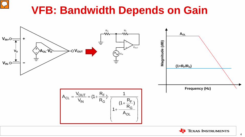
VFB: Bandwidth Depends on Gain
4
+
−
VIN+
VIN-
VD+− AOL∙VD VOUT
+
–
RFRG
VOUT
VIN
Frequency (Hz)
Mag
nitu
de (d
B)
AOL
(1+RF/RG)
OUT FCL
FIN G
G
OL
V R 1A (1 )RV R (1 )R1
A
= = + ⋅
+ +
Presenter
Presentation Notes
A conventional voltage-feedback amplifier consists of a high-input-impedance differential stage, followed by additional gain stages and a final low-output-impedance output stage. As shown in the figure, the voltage-feedback amplifier senses the differential error voltage between its inputs and amplifies it by the open-loop gain or AOL. Using control theory, the closed-loop gain is given by the equation shown here. Notice that the term in the denominator is in fact the low-frequency noise gain of the amplifier. Also, notice that in the above equation the -3dB bandwidth of the amplifier is given at the point where the magnitude of AOL is equal to the noise gain. The Bode plot shows the magnitude of the open-loop gain and noise gain. Remember that the closed-loop bandwidth of the amplifier is the frequency where AOL = (1+R F/R G) or the frequency at which the two curves intersect on the Bode plot. This intersection is also called the loop-gain crossover point. As the magnitude of the signal gain (and consequently the noise gain) increases, the two curves will intersect at a lower frequency. Conversely, as the signal gain decreases the curves will intersect at a higher frequency. This relationship is responsible for giving voltage-feedback op-amps their constant gain-bandwidth product behavior.
CFB: Bandwidth Independent of Gain
5
+
−
VIN+
VIN-
+− ZOL∙IN VOUT
α
INRi
+
–
RFRG
VOUT
VIN
INα ≈ 1
Loop gain is a function of the open-loop transimpedance, ZOL, and the
feedback transimpedance, (RF + Ri∙Noise Gain), of the amplifier.
OUT IN INN
F G
IN IN N i
OUT N OL
F
OUT GCL
FINF i
G
OL
F
G
FCL
FG
V V VI
R RAlso,V V I Rand, V I ZAfter further simplification,
R(1 )V R
Closed Loop Gain, ARV R R (1 )R1
ZR
1 and (1 ) Noise Gain, NGR
R 1A (1 )(R RR 1
− −
− +
+
−+ =
= α ⋅ − ⋅
= ⋅
α ⋅ += =
+ ⋅ ++
α ≈ + =
= + ⋅+
+ i
OL
NG)Z
⋅
If RF = 1 kΩ and Ri = 50Ω, and the amplifier is configured in a gain of 5V/V, then
the feedback transimpedance is (1000Ω + 5V/V∙50Ω ) = 1250 Ω
The noise gain scaling term (5V/V∙50Ω = 250 Ω ) has a relatively insignificant
effect on the magnitude of the numerator in the loop gain equation.
Presenter
Presentation Notes
A simplified block diagram of a current-feedback amplifier is shown here. Notice that the internal block diagram of a current feedback amplifier differs from its voltage feedback counterpart in two ways- A current feedback amplifiers input structure consists of a buffer between its noninverting and inverting inputs. The gain of the buffer is represented by alpha and is approximately equal to one. R i shown here is the output resistance of the buffer and plays an important role in the amplifiers dynamic performance. A 2nd point of contrast between the two amplifier types is that a current-feedback op-amp amplifies the error current IN at its inverting input while the voltage feedback opamp amplifies the error voltage between its inputs. I will explain the “error current” concept in detail in the subsequent slides. Since the current-feedback amplifier converts an error current into an output voltage its internal open-loop gain is represented by a transimpedance gain stage denoted by ZOL. This is analogous to the open-loop voltage gain, AOL, of a conventional voltage-feedback amplifier. A derivation for the closed-loop gain of a current-feedback amplifier is shown here. The loop-gain term in the denominator is a function of the transimpedance open-loop gain ZOL, the feedback resistance R F , the inverting input resistance R i and the noise-gain. The term R F + R i∙NG is referred to as the feedback transimpedance of the current-feedback amplifier . The effect of the feedback transimpedance of a current-feedback amplifier on its loop gain is analogous to the effect of the noise gain of a voltage-feedback amplifier on its loop gain. While a VFAs loop gain is dependent solely on its noise gain, in the case of a current-feedback amplifier the loop gain is dominated by the feedback resistance and the noise gain has a secondary effect. This concept is best explained through the use of a numerical example. The feedback resistance, R F, can range from a few hundred Ohms to a few kOhms, while R i is usually in the range of a few tens of ohms. For example if RF = 1kΩ and Ri = 50Ω, and the amplifier is configured in a gain of 5V/V, then the feedback transimpedance will be 1.25k Ω. The noise gain scaling term (250 Ω in this case) has a relatively insignificant effect on the magnitude of the numerator in the loop gain equation. Similar to the case of a voltage feedback amplifier, the 3dB bandwidth of the amplifier is determined by the frequency where the numerator and denominator term in the loop gain equation becomes equal. Thus for small values of gain, the feedback resistance will be the dominant factor in the numerator of the loop-gain term and will thus determine the bandwidth of a current-feedback amplifier. For the rest of this discussion, I will assume that the amplifier is configured in the non-inverting mode, thus making the closed-loop signal gain equal to the noise gain. Remember that in the inverting mode the noise gain = 1 + |inverting signal gain|.
+
–
RF= 866Ω RG= 96Ω
VOUT
VIN
IN
RL= 100Ω
CFB: Bandwidth versus Gain and RF
6
THS3091 Small-Signal Frequency Response versus Gain and RF
f − Frequency − Hz
Non
inve
rtin
g G
ain
− dB
1M 10M 100M 1G
2422201816141210
86420
-2-4
G= 10, RF= 866Ω
G= 5, RF= 1kΩ
G= 2, RF= 1.21kΩ
G= 1, RF= 1.78kΩ
RL= 100Ω,VO= 200mVPP,
VS= ±15V
Frequency (Hz)
Mag
nitu
de (d
B)
ZOL
RF + Ri.NG
LOAD F G iR || (R (R || R )) 89.6+ = Ω
, assuming Ri << RG
Presenter
Presentation Notes
This figure shows the small-signal frequency response of the THS3091, a high-voltage, low-distortion current-feedback amplifier. The THS3091s frequency response was measured as a function of its closed-loop gain, which was varied from 0 dB to 20 dB. The closed-loop bandwidth of the THS3091 remains almost constant at around 200 MHz irrespective of its closed-loop gain. Let us now study the Bode plot of a current feedback amplifier. The ZOL curve shown here in red has a low frequency dominant pole, and a high-frequency second-order pole (shown by the broken red line). The higher order pole reduces the phase margin in the same way that a higher-order AOL pole reduces the phase margin of a voltage feedback amplifier. The feedback transimpedance is also shown in blue. As the closed-loop gain of a current-feedback amplifier is increased, the total feedback transimpedance will also increase because of the finite value of R i. This increase is more pronounced at the higher gains where the product of Ri and the noise gain will be on par with the feedback resistance. The increase in feedback transimpedance will raise the blue curve, thus causing the loop-gain crossover to occur at a lower frequency. An increase in the feedback transimpedance increases the phase-margin and reduces the closed-loop bandwidth of the amplifier. In order to maintain a constant phase margin and bandwidth across gain, the feedback transimpedance should be kept constant. This is achieved by lowering the feedback resistance as the closed-loop gain is increased. Be cautious when configuring the amplifier in very high gains since one may be tempted to keep reducing the value of feedback resistance. However, remember that the feedback network is in parallel with the output load resistance, and reducing R F will increase the loading on the amplifiers output. The effective load on the amplifiers output is given by this equation. For example in a gain of 10, the effective load on the output of the THS3091 is will be 89.6 Ωs instead of a 100 Ωs. In summary, the feedback resistance is an integral part of the loop-gain equation; hence, the feedback resistance recommended in the datasheet should be adhered to in order to preserve stability.
CFB: Bandwidth versus Gain and RF (Cont.)
7
THS3091 Small-Signal Frequency Response versus RF
f − Frequency − Hz
Non
inve
rtin
g G
ain
− dB
1M 10M 100M 1G
9
8
7
6
5
4
3
2
1
0
RF= 750Ω
RF= 1.21kΩ
RF= 1.5kΩ
Gain= 6dB,RL= 100Ω,
VO= 200mVPP,VS= ±15V
Feedback Transimpedance =(RF + Ri × NoiseGain)
Presenter
Presentation Notes
This figure shows the small-signal frequency response of the THS3091 when the gain is kept constant and the feedback resistance is varied. The nominal feedback resistance is 1.21 kΩ. With a smaller value of R F the feedback transimpedance is reduced thus reducing the phase margin and increasing the bandwidth of the amplifier. The reduction in phase margin is apparent because of the peaking in the amplifiers frequency response. Similarly, when the value of R F is increased over the recommended value in the datasheet, the feedback transimpedance gets larger thus increasing the phase margin and decreasing the bandwidth. In this manner a current-feedback amplifier can be compensated for any arbitrary phase margin by changing the feedback resistance.
OPA691 Recommended Gain vs. RF
8
Feedback Transimpedance =(RF + Ri × NoiseGain)
Using the Feedback transimpedance equation for gains of 2V/V
and 5V/V:
400Ω + (2·Ri) = 300Ω + (5·Ri)
⇒ Ri = 33.33 Ω
Target Feedback transimpedance for OPA691:
400Ω + (2·35 Ω) = 470Ω
Presenter
Presentation Notes
In order to simplify the circuit design for the customer, current feedback amplifier datasheets have a graph or a table which shows the recommended value of feedback resistance as a function of the noise gain. An example graph for the OPA691 is shown here. Remember that in order to maintain a constant bandwidth across gain the feedback transimpedance should be kept constant. Based on this graph we can then extract the value of Ri by substituting the values for gain and RF for two different gain configurations. For example: Substituting the value of feedback resistance from the graph in a gain of 2 and 5 respectively into the feedback transimpedance equation and equating the two results in an Ri of 33.33 Ω. This value matches quite closely with the specified 35Ω in the electrical characteristics table of the datasheet. Once the value of Ri is known the targeted feedback transimpedance for a CFB can be determined using the now familiar equation. In the case of the OPA691 the target feedback transimpedance is 470 Ω.
Estimating f-3dB from ZOL curve
9
Target Feedback transimpedance for OPA691:
400Ω + (2·35 Ω) = 470Ω = 53.4 dBΩ
Presenter
Presentation Notes
The closed loop bandwidth of a current feedback amplifier can be estimated from the open-loop transimpedance curve once the target feedback transimpedance is known. The OPA691s target feedback transimpedance was calculated in the previous slide to be around 470 Ω or 53.4dBΩ. As shown in the figure above the intersection between 54dBΩ and the Zol curve occurs around 100 MHz. The electrical characteristics table in the datasheet however specifies the bandwidth in a gain of 2 to be 190MHz. There are a few reasons for the discrepancy between the measured value of a 190MHz and the calculated value of 100MHz. The equation for the feedback transimpedance is based on a single-pole 1st order system. However the open loop ZOL curve shown is that of a 2nd order system as evident by the 180° phase shift in the amplifiers open loop phase response. The reduction in phase margin in a 2nd order system will extend the closed loop bandwidth of the amplifier and is partially responsible for the increase in bandwidth from a 100MHz to a 190 MHz. Another reason for the discrepancy between theory and measurement is that value of Ri is not constant across frequency and amplitude while the calculations so far assumed Ri to be constant at 35 ohms.
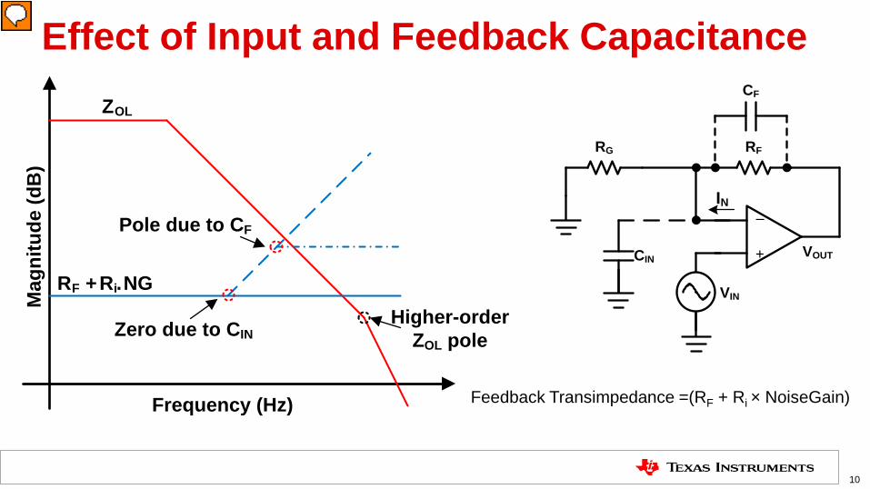
Effect of Input and Feedback Capacitance
10
+
–
RFRG
VOUT
VIN
IN
CF
CIN
Frequency (Hz)
ZOL
RF + Ri.NG
Mag
nitu
de (d
B)
Higher-order ZOL poleZero due to CIN
Pole due to CF
Feedback Transimpedance =(RF + Ri × NoiseGain)
Presenter
Presentation Notes
Input capacitance, is inherent to an opamps internal architecture and is also present as a parasitic in the PCB traces. The input capacitance interacts with the feedback resistance to create a zero in the noise-gain response which consequently introduces a zero in the feedback transimpedance as shown here. The trace capacitance can be minimized by removing the PCB ground plane around the inverting terminal. As discussed previously, in order to maintain a constant feedback transimpedance across gain, RF must be increased as the gain is reduced. The increased RF at lower signal gains results in a reduced zero frequency. A zero in the noise gain response is a pole in the loop gain response. Remember that a pole in the loop gain response reduces the amplifiers phase margin. To counter the effect of the zero a pole can be introduced into the feedback transimpedance curve by adding a feedback capacitance CF in parallel with RF. This compensation technique is similar to the lead-lag technique commonly used to stabilize voltage-feedback amplifiers.
Effect of Non-Ideal RF and CF
Frequency (Hz)
ZOL
Mag
nitu
de (d
B)
Higher-order ZOL pole
Frequency (Hz)
ZOL
RF + Ri.NG
Mag
nitu
de (d
B)
Higher-order ZOL pole
Zero due to CIN
Pole due to CF
RF + Ri.NG
Effect of RF << Recommended datasheet valueEffect of CF >> CIN
+
–
RF
VOUT
VIN
Unity Gain Config.
11
Presenter
Presentation Notes
Now the next point is very important! Do not add a feedback capacitor unless the circuit analysis requires it. If the input capacitance is negligible and a large feedback capacitance is added, then the pole will occur before the zero as shown here. The net effect of the pole occurring before the zero is a reduction in the feedback transimpedance which causes the loop-gain crossover to occur closer to the higher order ZOL pole which reduces the amplifiers phase margin. The feedback resistance used at a given closed-loop gain should not be too far below the recommended value in the datasheet since this can cause the loop-gain crossover to occur after the higher order ZOL pole thus reducing the phase margin (as shown here). When configuring the amplifier as a unity-gain buffer, one may be tempted to set the feedback resistance, R F = 0 Ω and thus short the output of the amplifier to its inverting input, like a traditional voltage feedback amplifier. A feedback resistance of 0Ω will cause the loop gain crossover to occur after the 2nd pole in the ZOL curve greatly reducing the amplifiers phase margin and should thus be avoided. The datasheet of CFA usually specifies the feedback resistance to be used in unity-gain configurations.
12
Thanks for your time and please
take the quiz!
Presenter
Presentation Notes
So to highlight some of the key factors to keep in mind when designing systems that use current feedback amplifiers - Pay attention to the datasheet recommended values of feedback resistance when using CFBs. By maintaining a constant value of feedback transimpedance A CFB is capable of holding a constant bandwidth and phase margin across gain. Thank you for your time and please take the quiz.