Embed Size (px)
Citation preview

COMBINATIONAL LOGIC CIRCUITS

In Chapter Three individual gates were investigated. This chapter will use those gates in combination to produce more complex logic functions. Techniques for simplifying these complex functions will also be covered.
Simplification of logic circuits is a responsibility of the designer. Simpler circuits are generally more economic and more reliable. The economy is achieved by using fewer integrated circuits while reliability is achieved by having fewer solder connections in the finished product.
4.0 INTRODUCTION

Upon completion of this chapter you should be able to:
• Simplify logic expressions.
• Simplify logic circuits.
• Use the Karnaugh map to simplify logic circuits andexpressions.
4.1 OBJECTIVES
41

4.2 SUM-OF-PRODUCT FORM
The sum-of-product form of a logic circuit output looks like the following examples:

f = AB + ABC + CD
These examples show that the output of a logic circuit represented by x, z, or f are a logic one, or are true, when any of the logic products separated by the OR (+) designation are satisfied. The logic expressions completely define a logic circuit's operation in terms of the state of the logic inputs.
Logic equations may be formed directly from a truth table. These equations may also be simplified using Boolean algebra or more mechanical methods. Both types of simplification will be covered. The logic equations shown in the above examples are called "minterm" expressions.
Minterm expressions are logical equations where the logical product terms are separated by the logical sum operator. Minterm expressions are formed directly from truth tables. Minterm expressions are also called sum-of-product expressions.

4.3 DESIGNINGCOMBINATION
CIRCUITS
Logic design begins with a problem statement. The problem statement is analyzed and translated into logic variable inputs. A truth table is then constructed to show when a logic one output is to be produced. Next a sum-of-product (minterm) logic equation is then produced. Then a circuit is drawn from the sum-of-product logic equation. These steps are illustrated by the following example.
Problem statement: An alarm is to be used in an automated ink bottling plant. A conveyer belt carries the empty ink bottles past the filling spout. The alarm is to sound if any of the following conditions occur:

42

A. The ink tank runs empty.
B. There are no bottles on the conveyor belt even if ink is inthe tank.
C. There is ink in the tank, bottles on the conveyor belt, andelectric power is lost.
The first step is to assign variables to the inputs.
I = ink in the tank
B = bottles on the conveyor belt
P = electric power is on
Next a truth table is constructed using these variables for inputs and indicating when the alarm is to ring by placing a one in the output, X, column. A minterm expression is then written. (See Table 4-1)

Table 4-1 has a one in the output, X, for all cases where ink is not present (I). In fact, the truth table shows that the alarm will not sound, X=0, when ink is present and bottles are present and power is on. Any other condition will sound the alarm.
Analyzing the minterm or sum-of products expression shows that the alarm system may be directly implemented by using a seven input OR gate with each input being fed by a three input AND gate. This circuit implementation is shown in Figure 4-1.


43


Figure 4-1 could be further complicated by including inverter circuits to form the "NOT" inputs. This circuit will fulfill the design objective of the problem, but may not be the simplest circuit.

4.4 BOOLEAN SIMPLIFICATION
One method of circuit or minterm simplification is to use Boolean algebra l:o remove logic redundancy. This method is based on the Boolean single and multivariable theorems. The Boolean theorems are summarized in Table 4-2.

44

The first term of the original expression can be used again with the last term of the expression:
X="IB + IB + IB + P
Combining the first term with both the second and third terms
give:
This final expression is logically equivalent to the original minterm expression. Figure 4-2 shows the final simplified circuit to implement the alarm system of the original problem. This solution is simpler, less expensive, and more reliable.

Boolean algebra can be used for logic circuit simplification, but most students find the Karnaugh map technique to be easier. The Karnaugh map technique will be discussed shortly.

DeMorgan's theorem is important enough to command its own major heading in any digital text. DeMorgan's Theorem will allow the expression of logic equations in maxterm or product-of-sum form. (See Figure 4-3)
4.5 DEMORGAN'S THEOREM

Since there are only two logic operators besides the NOT function, DeMorgan's Theorem simply states that if an operator is NOTed it becomes the other. The OR operator NOTed becomes the AND operator and if the AND operator is NOTed it becomes the OR logic operator. The importance of this Theorem will become increasingly apparent in following discussions.


45

4.6 THE KARNAUGH MAP
The Karnaugh map or K-map technique is a graphical device to simplify logic equations or the output of truth tables following a simple orderly process. The K-map technique can be used for any number of variables, but becomes a little hard to handle when more than lour input variables are considered. For this reason, the discussion of this technique will be limited to cases having no more than four input variables.
A K-map like a truth table displays the relationship between input variables and the desired or true output of a logic expression or truth table. The K-map presents this information as entries in boxes of a K-map rectangle. Figure 4-4 gives three examples. The examples become more complex as more input variables are involved. Note that each box in a K-map identifies a specific and unique combination of the input variables.


In viewing Figure 4-4, the following points should become apparent:
1. The logic equations, truth tables, and K-maps contain thesame information.
2. The addition of an input variable doubles the number ofentries in the truth tables and K-maps.
3. The K-maps are organized in a precise way. The entriesacross the top and down the sice of the K-map arearranged so that only one variable changes. Thesepatterns should be carefully and faithfully observed.
Once a K-map has been constructed for a problem. The entries may be looped. The loops are formed around adjacent l's. The l's may be looped in groups of one, two, four, or eight. Examples of looping are shown in Figure 4-5. Each loop of a K-map represents a single term in the simplified logic equation-larger and fewer loops result in the most simplification.


47

48

1. Construct the K-map from the original equation or truthtable.
2. Carefully examine the K-map for adjacent l's and loopthe largest number of adjacent Is (two, lour, or eight).
3. Loop any pairs necessary to include any adjacent l's thathave not yet been included in a loop.
4. Loop any remaining single or isolated l's.
5. Any variable appearing in a loop in both its true andcomplemented form is eliminated.
6. Form the simplified sum of products equation from allthe terms generated by the loops.
Figure 4-6 shows some examples of the power of using the K-map technique. Both the original and simplified logic equation is given for each example.


In the examples, each loop that is drawn results in a single term of the simplified equation. Ones may be used in more than a single loop as shown in the second example. Isolated ones become the most complex terms, as shown in the second example.
This technique can be applied to the ink factory alarm logic of the original example shown in Table 4-1. Figure 4-7 shows the original equation, the K-map with loops drawn, and the final simplified equation. Note that the simplified equation is the same as the one obtained by applying Boolean algebra.

50

Figure 4-8 shows how careful consideration in recognizing "don't care" conditions and later changing "don't cares" to ones or zeros can greatly simplify a logic design. The trick is to recognize early in the design any "don't, care" conditions and identify them by using X instead of 1 or 0 in the truth table.


The opening section of this chapter discussed the sum-of-product form of equations. The implication was that there are other ways to express a logic equation. Th.s other way is called the product-of-sums form. Figure 4-9 gives examples of this form for logic equations.
4.7 PRODUCT-OF-SUMS FORM

To create the product-of-sums form involves the use of DeMorgans Theorem. An example will be helpful in illustrating the concepts involved.

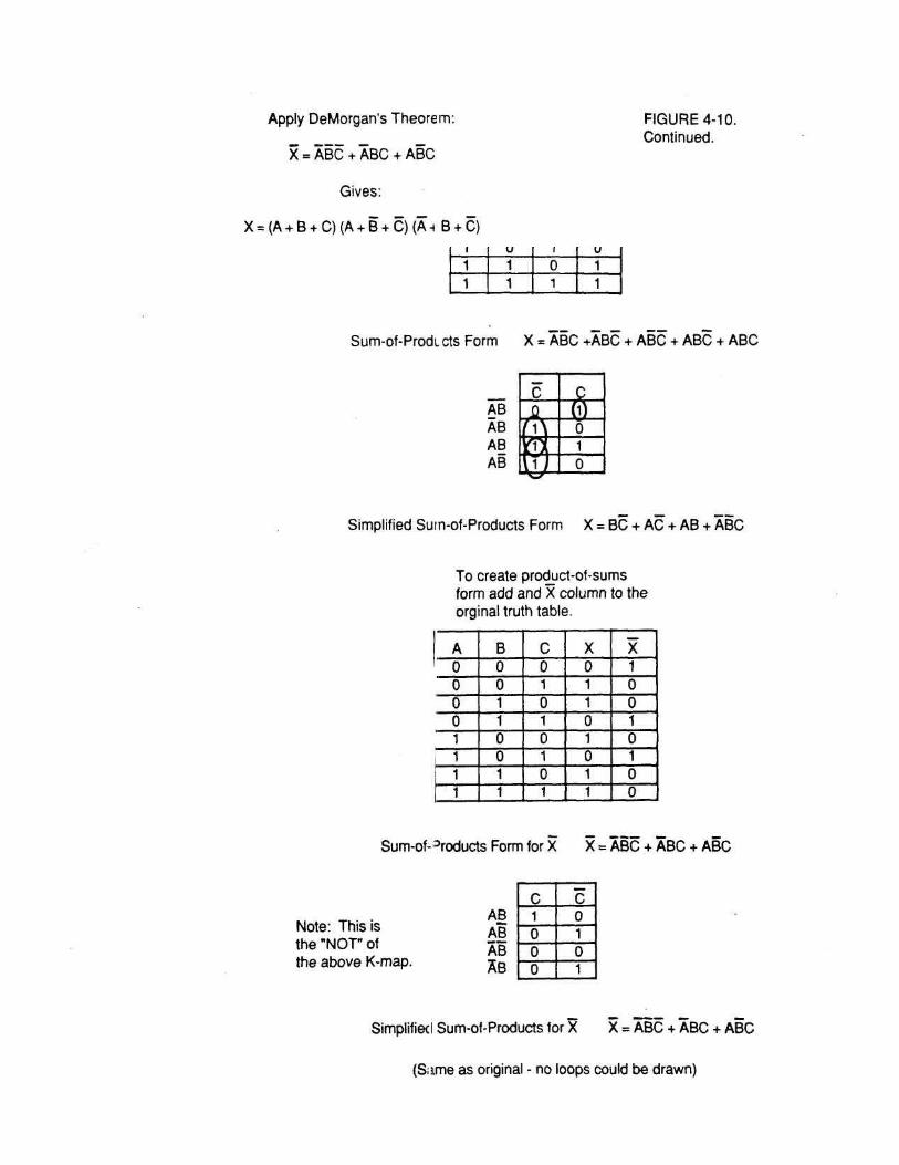

In Figure 4-10, the final product of-sums equation is logically equivalent to the original sum- of-products equation. Figure 4-11 shows how these two equations would be implemented.


The two logic circuits are equivale it.
The reason for interest in having two forms for logical equations is ease of implementation when using universal logic gates; NAND and NOR. The sum-of-prod .ict form is most easily implemented using all NAND gates, while the product-of-sums form is most easily implemented using all NOR gates. The examples given in Figures 4-10 and 4-11 are shown implemented using all NAND or all NOR g ates.

53


The circuit using only NAND gates is logically equivalent to the circuit using only NOR gates. This can be verified by setting all possible input states to the two circuits and observe coincidence in th<; outputs.

4.8 THE EXCLUSIVE OR AND
EXCLUSIVE NOR CIRCUITS
The final topic of this chapter deals with two gate structures that are not basic £;ate structures, but whose functions occur so frequently that they have earned their own symbols. These gate structures are often used in comparator circuits. Figure 4-13 indicates the symbols and truth tables for these logic gates.

54

The output of the Exclusive OR gate is true only when the two inputs are different. The output of the Exclusive NOR gate is true only when the two inputs are equa'. Each of these gates may be produced using AND, OR, and NOT ,;ates.


This chapter has introduced Boolean algebn and Karnaugh map techniques for simplifying logic circuits. Both single variable and multivariable theorems were covered as well as DeMorgan's theorem.
Product-of-sums and sum-of-products as two forms of logic gates were introduced. Each of these foms are more easily implemented by either NAND or NOR universal gates.
Two important gate functions; the Exclusive OR and the Exclusive NOR were introduced.
4.9 SUMMARY

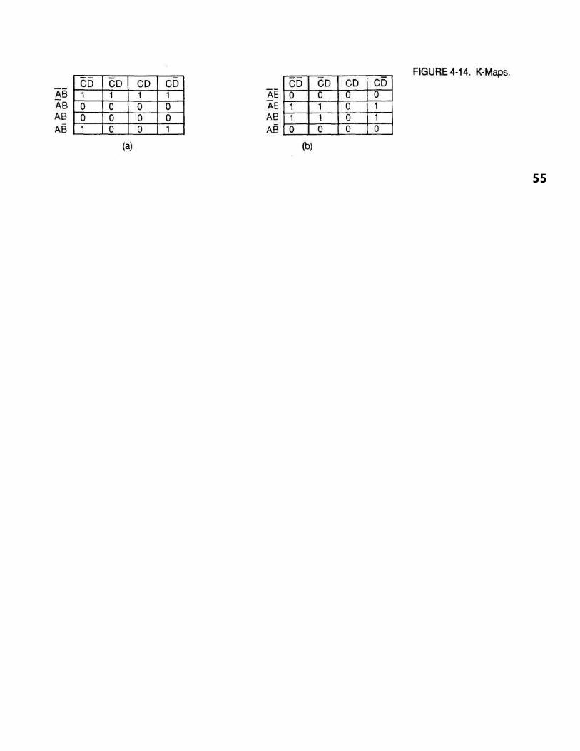
1. Determine the simplified logic equation for each of the K-maps in Figure 4-14.
4.10 REVIEW QUESTIONS
55

56
2. Write the original equations used to form the K-maps of
Figure 4-14.
(a)______________________________________________________
(b)_____________________________________________________
(c)______________________________________________________

3. Sketch the outputs for the inputs shown in Figure 4-15.

4. In the space below, show how Exclusi ve OR and Exclusive NOR circuits are constructed from AND, OR, and NOT gates.


57

LAB EXERCISE 4.1Minterm and
Maxterm TruthTables
Objectives
Materials
Procedure
In this lab exercise you will learn the use of minterm and maxterm truth tables. You will also demonstrate the equivalence of tie minterm and maxterm forms of a logic expression.
CA.D.E.T.
74LS08 Quad 2-Input AND
74LS04 Hex Inverters
74LS11 Tr pie 3-Input AND
74LS32 Qi ad 2-Input OR
Jumper W ires(Refer to Jappendix for IC pinouts)
1. The truth ta bles used in this book until now have been minterm truth tables. Logic equations can be directly written from these tables in th; sum of products form. (See Figure 4-16).

58

2. Insert a 74LS08 and 74LS04 in the breadboard of the C. A.D.E.T. Wire the power (+5 VDC) and ground pins for the ICs.
3- Wire LSI (Logic Switch 1) to pin 1 of th 2 74LS04 and to LI1 (Logic Indicator). Wire pin 2 of the 74LS04 to pin 1 of the 74LS08. This is for the A input.
4. Wire LS2 to LI2 and pin 2 of the 74LS08. LS2 will serve as the B

input.
5- Wire LI3 to pin 3 of the 74LS08. This is the circuit output.
Switch LSI & LS2 to LOW. Turn power ON.
7.LSI and LS2 are the A and B inputs which can be observed on LI1and LI2. Use LSI, LS2 and LS3 to dete rmine a truth table for this logic circuit. Record this truth table.


59
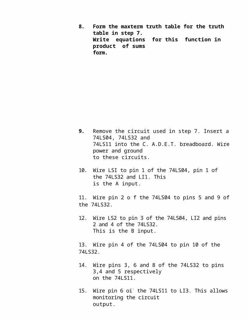
8. Form the maxterm truth table for the truth table in step 7.Write equations for this function in product of sumsform.
9. Remove the circuit used in step 7. Insert a 74LS04, 74LS32 and74LS11 into the C. A.D.E.T. breadboard. Wire power and groundto these circuits.
10. Wire LSI to pin 1 of the 74LS04, pin 1 of the 74LS32 and LI1. Thisis the A input.
11. Wire pin 2 o f the 74LS04 to pins 5 and 9 of the 74LS32.
12. Wire LS2 to pin 3 of the 74LS04, LI2 and pins 2 and 4 of the 74LS32.This is the B input.
13. Wire pin 4 of the 74LS04 to pin 10 of the 74LS32.
14. Wire pins 3, 6 and 8 of the 74LS32 to pins 3,4 and 5 respectivelyon the 74LS11.
15. Wire pin 6 oi: the 74LS11 to LI3. This allows monitoring the circuitoutput.
16. Switch all logic switches to LOW. Turn ON power.
17. LSI is A, LS2 is B, and LI3 is the logic circuit output. Use LSI, LS2,and LI3 to construct a truth table for this circuit. Record the truthtable here. Leave the circuit connected and answer the followingquestions.
60

1. Compare the truth tables from steps 7 and 17. What doyou notice about them?
2. Draw schematic diagrams of the circuits that producedthe truth tables in steps 7 and 17.
3. Which circuit better performs this logic function ? (step 7or step 17?). Why?
Questions

In this lab exercise you will study and apply techniques to reduce redundant logic elements in combinational logic circuits.
LAB EXERCISE 4.2 Simplifying Logic CircuitsObjectives

61

62
Materials
Procedure
C.A.D.E.T. 74LS04 Hex
Inverter 74LS08 Quad 2-
Input AND 74LS27 Triple 3-
Input NOR 74LS32 Quad 2-
Input OR
Jumper Wires(Refer to Appendix for IC pinouts.)
1. A truth table for a logic function is shown in Figure 4-18. From this itruth table write the sum of products form of the logic equation represented by the truth table.
2. Insert a 74LS04, 74LS08 and 74LS27 into the C.A.D.E.T. breadboard. Wire power and ground to these ICs.
3. Wire LSI to 74LS04 pin 1, 74LS08 pin 9 and LI1. This is the Ainput.
4. Wire 74LS04 pin 2 to 74LS08 pins 1 and 4.
5. Wire LS2 to pin 3 of the 74LS04, pin 5 of the 74LS08, and LI2. Wire74LS04 pin 4 to 74LS08 pins 2 and 10. This is the B input.
6. Wire pins 3,, 6, and 8 of the 74LS08 to pins 3, 4, and 5, respectively,of the 74LS27.
7. Wire pin 6 of the 74LS27 to pin 5 of the 74LS04. Wire pin 6 of the74LS04 to LI3. This is the circuit output.
8. The schematic for the circuit constructed is shown inFigure 4-19.

9. Switch all logic switches to LOW. Turn ON power. LI3 shouldshow a HIGH.
10. Use LSI, LS2, and LI3 to construct a truth table for this circuit.Record the truth table here.
11. This circuit has redundant elements. It could beconverted to function the same with fewer components.We shall use Karnaugh maps to reduce the logiccircuitry.
12. A generalized Karnaugh map for two variables is shownin Figure 4-20.
13. Use the truth table to fill the Karnaugh map with ones where appropriate. Form loops on the map. Record your results.


63

14. Write the simplified logic equation for this map here.

Questions

15. Remove the previous circuit from the breadboard. Put a74LS04 and a 74LS32 onto the breadboard and wire powerand ground to them.
16. Wire LS2 to pin 1 of the 74LS04 and Ul. Wire pin 2 of the 74LS04to pin 1 of the 74LS32.
17. Wire LS2 to pin 3 of the 74LS04 and LI2. Wire pin 4 of the 74LS04to pin 2 of the 74LS32.
18. Wire pin 3 of the 74LS32 to LI3.
19. Switch all logic switches to LOW and turn ON power. LI3 shouldshow a HIGH.
20. LSI is A, LS2 is B and LI3 the circuit output. Use LSI, LS2, and LI3to construct a truth table for this circuit. Record your observations.
21. Leave this circuit connected while you answer thefollowing questions.
1. What is the common name for the logic function displayed in the truth table in step 1?
64

2. What do you notice about the truth tables resulting fromsteps 10 and 20 ?
3. What do you call the simplified logic equation from theresults of step 14 ?
4. Which of the circuits is better to use? Why?

You will learn about decoders in this lab exercise. You will study the simple decoder and the one of four decoder.
C.A.D.E.T. 74LS04 Hex
Inverter 74LS08 Quad 2-
Input AND 74LS11 Triple 3-
Input AND
Jumper Wires(Refer to Appendix for IC pinouts.)
1. The simple decoder will be studied first. A decoder detects the presence of a specific binary number or word. The decoder is usually formed from AND and NOT gates. Decoders are used extensively in computers for enabling memory and I/O devices.
LAB EXERCISE 4.3DecodersObjectives
Materials
Procedure

65

2. Place a 74LS11 on the C.A.D.E.T. breadboard. Wire the circuit shown. (See Figure 4-21)


3. Switch all logic switches to LOW and apply power.
4. Use LSI, LS2, LS3, and LI1 to determine the truth table for thiscircuit. Record your observations here.

5. Turn off power and remove the circuit from step 4.
6. Place a 74LS04 and a 74LS08 on the C.A.D.E.T. breadboard. Wirepower and ground for these circuits.
7. Wire the circuit shown in Figure 4-22. This circuit is aone of four decoder.

66

8. Turn the logic switches to LOW. Turn ON power. LI1 should showa HIGH.
9. Use LSI, LS2, and LI1-LI4 to form a table of the circuit operation.
10. Leave the circuit wired while you answer the followingquestions.

1. What binary number does the circuit from Step 4 decode?
2. Name one use of a circuit like the one in Figure 4-6.
3. Explain the operation of the one of four decoder.
4. Design a circuit to decode 101 binary.
5. Circuits similar to the one of four decoder are used toconvert from BCD to decimal. How many AND gateswill be required to implement such a circuit ? Hint:Examine Figure 4-22 schematic.
Questions

67

6. Why can't the logic equation from the truth table of step 9 be written as y = AB + AB + AB + AB ?

LAB EXERCISE 4.4 Encoders
Objectives
Materials
In this lab exercise encoders will be studied. Encoders accept one or more inputs and generate a mutli-bit binary output. You will study a simple encoder. The basic encoder circuit is the positive NAND gate.
C.A.D.E.T.
74LS00 Quad 2-Input NAND
Jumper Wires(Refer to Appendix for IC pinouts.)

Procedure 1. Wire the circuit shown in Figure 4-23. Note that PB1 and PB2, the C. A.D.E.T. pushbuttons, have normally high and normally low connections. (See Figure 3.10)

68
2. Switch LS3 to LOW. Turn ON power.
3. Press PB1, PB2, and LS3 one at a time. Note: LS3 will have to bemanually returned to HIGH. PB1 and PB2 return on their own.
4. Describe what happens when PB1 is pressed.

2. Record your observation when PB2 is pressed.
3. Place LS3 to LOW. Record your observations.
4. Return LS3 to HIGH.
5. Remove power from the circuit.
1. What does the circuit of step one do ? Questions

In this lab exercise the exclusive OR (EXOR) circuit and some applications of EXOR circuits will be studied.
C.A.D.E.T. 74LS04 Hex Inverter
74LS08 Quad 2-Input NAND
74LS32 Quad 2-Input OR 74LS86
Quad EXOR
Jumpers(Ref. to Appendix for IC pinouts.)
LAB EXERCISE 4.5 Exclusive OR Circuits
Objectives
Materials

69

Procedure 1 The truth table for the exclusive OR function is shown in Figure 4-24.


2. The logic expression for this truth table is y = AB + BA.
3. Wire a circuit from the schematic in Figure 4-25.

4. Switch the logic switches to LOW and turn ON power.
5. Use LSI, LS2, and LI3 to form the truth table for this circuit. Record your observations here.
6. Notice that the circuit detects when the inputs are odd (not matched). For this reason, the EXOR is often called an odd/even detector.
70

7. Turn OFF power to the circuit. Remove the ICs from thebreadboard.
8. Place a 74LS86 into the C. A.D.E.T. breadboard.
9. Wire the circuit shown in Figure 4-26.

10. Switch logic switches to LOW and power ON.
H. Use LSI, LS2, and LI3 to form a truth table for this circuit. Record the truth table here.
12. You have focused on the logic circuit uses of the EXOR. The EXOR also performs a binary math function.
1. Examine the truth tables from steps 1, 5, and 11. What do you notice about them?

Questions

71

2. What math function does the EXOR gate perform ?
3. Which circuit is better to use, the one from step 3 or theone from step 9? Why?
4. Draw the Karnaugh map for the EXOR. Can this bereduced?

LAB EXERCISE 4.6 The EXNOR Circuit
Objectives
Materials
In this lab exercise the EXNOR circuit will be studied.
CA.D.E.T.
74LS04 Hex Inverter
74LS86 Quad EXOR

72
1. Wire the circuit shown in the schematic of Figure 4-27. Procedure

2. The EXNOR logic function is the complement of theEXOR.
3. Use LSI, LS2, and LI3 to determine the truth table for thiscircuit. Record the truth table here.
4. Note that the EXNOR compares the value of A and B andoutputs a 1 when the inputs are equal.
5. Remove the wire from LS2 and wire it to PB1 normally low.(See Figure 1 OB).
6. Operate LSI while observing LI3. Record your observations.
5. Write the EXNOR logic equation directly from thetruthtable.
6. What function does the circuit of step five perform ?

Questions

73

3. Make a Karnaugh map for the EXNOR function. Can this function be reduced ?

74