Embed Size (px)
Citation preview

S1
Supporting Information
CsPb0.9Sn0.1IBr2 Based All-Inorganic Perovskite Solar Cells with
Exceptional Efficiency and Stability
Jia Liang,1 Peiyang Zhao,
1 Caixing Wang,
1 Yanrong Wang,
1 Yi Hu,
1 Guoyin Zhu,
1 Lianbo Ma,
1
Jie Liu,1,2
and Zhong Jin1,*
1 Key Laboratory of Mesoscopic Chemistry of MOE, School of Chemistry and Chemical
Engineering, Nanjing University, Nanjing, Jiangsu 210023, China
2 Department of Chemistry, Duke University, Durham, North Carolina 27708, USA
*E-mail address of corresponding author: [email protected]

S2
Experimental Details
Preparation of c-TiO2 and m-TiO2 layers on FTO substrates. FTO glass substrates was first
etched by Zn powder and 2.0 M HCl for desirable patterns. Then, the patterned FTO substrates
were sequentially ultrasonic cleaned with acetone, ethanol and pure water. Subsequently, a thin
layer of c-TiO2 layer was deposited on the FTO electrodes by spin-coating an ethanol solution of
titanium isopropoxide (0.5 M) and diethanol amine (0.5 M) at 7,000 rpm for 30 s, followed by
annealing in air at 500 °C for 2 h. The m-TiO2 layer was deposited on the c-TiO2 layer by spin-
coating a mixture of TiO2 nanoparticle paste (20 nm diameter) and ethanol with the weight ratio
of 1:8 at 5,000 rpm for 30 s, dried at 120 °C for 10 min, and then annealed at 500 °C for 30 min.
Afterward, the FTO substrates were immersed in a 40 mM TiCl4 aqueous solution at 70 °C for
30 min. Then, the FTO/c-TiO2/m-TiO2 substrate was cleaned with water and ethanol, and then
annealed at 450 °C for another 30 min.
Preparation of all-inorganic PSCs based on CsPbBr3, CsPbIBr2, and CsPb0.9Sn0.1IBr2 films.
Different from the traditional organic-inorganic hybrid perovskites, the preparation of inorganic
perovskites in this study, including CsPbBr3, CsPbIBr2, and CsPb0.9Sn0.1IBr2, can be conducted
in ambient atmosphere without humidity control (with relative humidity (RH) up to 90%).
Typically, 1.0 mmol of solid precursor (PbBr2 for CsPbBr3 and CsPbIBr2; or the mixture of
PbBr2 and SnBr2 with a molar ratio of 0.9:0.1 for CsPb0.9Sn0.1IBr2) was dissolved in the mixed
solvents of N,N-dimethylformamide (DMF) and (DMSO) (4:1 in volume) under stirring at 80 °C
for 30 min to yield a 1.0 M precursor solution. Then, the solution was deposited on the FTO/c-
TiO2/m-TiO2 substrate by spin-coating at 2,000 rpm for 30 s, followed by drying at 80 °C for 30
min. After that, the prepared film was dipped in a 15 mg/mL methanol solution of cesium salt
(CsBr for CsPbBr3; or CsI for CsPbIBr2 and CsPb0.9Sn0.1IBr2) for 10 min. Subsequently, the as-
obtained yellow films were thoroughly rinsed with isopropanol, and then heated for 10 min in air
on a hotplate (250 °C for CsPbBr3; or 350 °C for CsPbIBr2 and CsPb0.9Sn0.1IBr2). Then, the
carbon electrode served as both HTM and counter electrode was deposited on the inorganic
perovskite layer by doctor-blade coating of conductive carbon ink and then heated at 70 °C for
60 min. For encapsulation, the all-inorganic PSC was sealed by cover glass and hot-melt spacer
(Surlyn 1702, 30 μm thick, Solaronix).

S3
Preparation of CsPb0.9Sn0.1I2Br films. As control samples, CsPb0.9Sn0.1I2Br films with higher
content of I element (I/Br ratio = 2:1) were also prepared through the same preparation process
for CsPb0.9Sn0.1IBr2 films (I/Br ratio = 1:2) as described above, except that the mixture of PbBr2
and SnBr2 was replaced by PbI2 and SnI2 with a molar ratio of 0.9:0.1, and the CsI solution was
replaced by CsBr solution.
Preparation of Cs0.9MA0.1Pb0.9Sn0.1IBr2 films. For comparison, Cs0.9MA0.1Pb0.9Sn0.1IBr2 films
were also prepared through the same preparation process for CsPb0.9Sn0.1IBr2 films, except that
the CsI solution was replaced by the mixed solution of CsI and MAI with a molar ratio of
0.9:0.1.
Characterizations. To obtain the surface and cross-section morphologies, SEM
characterizations were performed with a FEI Nova450 instrument. EDX analysis was performed
with the Bruker QUANTAX accessory attached on the SEM. XRD spectra were measured by a
Bruker D-8 Advance diffractometer with Cu Kα X-ray radiation. XPS analyses of elemental
binding energies and VBM positions were carried out with a PHI-5000 VersaProbe X-ray
photoelectron spectrometer with Al Kα X-ray radiation. Before testing the photophysical
properties and photovoltaic performances, the as-prepared all-inorganic PSCs were illuminated
under simulated AM1.5G solar light using a solar simulator (100 mW/cm2, NOWDATA SXDN-
150E) for about 15 min in advance for activation. The absorbance spectra of inorganic perovskite
films were measured using a Shinadzu UV-2456 spectrophotometer. The photoluminescence
(PL) spectra were recorded on a home-built wide-field fluorescence microscope under the
excitation wavelength of 450 nm. The J–V curves were measured with a Keithley 2400 Source
Meter under AM 1.5G illumination. The light intensity was calibrated with a standard Si solar
cell for 1 sun. Typically, the active area of the all-inorganic PSCs in this study is 0.09 cm2. The
IPCE spectra were measured as a function of wavelength controlled by a monochromator.
S4
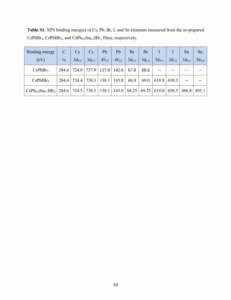
Table S1. XPS binding energies of Cs, Pb, Br, I, and Sn elements measured from the as-prepared
CsPbBr3, CsPbIBr2, and CsPb0.9Sn0.1IBr2 films, respectively.
Binding energy
(eV)
C
1s
Cs
3d5/2
Cs
3d3/2
Pb
4f7/2
Pb
4f5/2
Br
3d5/2
Br
3d3/2
I
3d5/2
I
3d3/2
Sn
3d5/2
Sn
3d3/2
CsPbBr3 284.6 724.0 737.9 137.8 142.6 67.8 68.6 -- -- -- --
CsPbIBr2 284.6 724.4 738.3 138.1 143.0 68.0 69.0 618.9 630.3 -- --
CsPb0.9Sn0.1IBr2 284.6 724.5 738.5 138.1 143.0 68.25 69.25 619.0 630.5 486.8 495.1

S5
Table S2. Typical photovoltaic parameters of all-inorganic PSCs based on CsPbBr3, CsPbIBr2,
and CsPb0.9Sn0.1IBr2, respectively.
Light absorber JSC ( mA/cm2) VOC (V) FF PCE (%)
CsPbBr3 7.34 1.25 0.63 5.82
CsPbIBr2 12.32 1.08 0.62 8.25
CsPb0.9Sn0.1IBr2 14.30 1.26 0.63 11.33

S6
Table S3. Performance comparison of existing PSCs based on CsMX3 inorganic perovskites.
Reference Light absorber ETL, HTL, Counter
electrode
JSC
(mA/cm2)
VOC
(V) FF
PCE
(%)
This work CsPb0.9Sn0.1IBr2 TiO2, Carbon 14.30 1.26 0.63 11.33
[14] CsPbBr3 TiO2, PTAA, Au 6.24 1.28 0.74 5.95
[15] CsPbBr3 TiO2, PTAA, Au 6.7 1.25 0.73 6.2
[16] CsPbBr3 TiO2, Carbon 7.4 1.24 0.73 6.7
[18] CsPbI3 TiO2, Spiro-OMeAD, Au 12 0.8 - 2.9
[19] CsPbI3 TiO2, Spiro-OMeAD,
MoOx & Al 13.47 1.23 0.65 10.77
[20] CsPbI3 TiO2, Spiro-OMeAD, Ag 11.92 0.66 0.52 4.13
[21] CsPbI3 TiO2, P3HT, Au 13.8 1.063 0.716 10.5
[22] CsPbI3 PCBM, PEDOT:PSS, BCP
& LiF & Al 8.26 0.95 0.67 5.38
[23] CsPbI3 TiO2, Carbon 14.31 0.67 0.48 4.65
[24] CsPbI2Br TiO2, Spiro-OMeAD, Ag 11.89 1.11 0.75 9.84
[25] CsPbI2Br PCBM, PEDOT:PSS, BCP
& Al 10.9 1.06 - 6.8
[26] CsPbIBr2 TiO2, Au 8.7 0.96 0.56 4.7
[27] CsPbIBr2 TiO2, Spiro-OMeAD, Au 7.8 1.13 0.72 6.3
[28] Cs0.925K0.075PbI2Br TiO2, Spiro-OMeAD, Au 11.6 1.18 0.73 10.0
[29] CsSnI3 TiO2, Spiro-OMeAD, Au 22.7 0.24 0.37 2.02
[30] CsSnBr3 TiO2, PTAA, Au 13.96 0.37 0.59 3.04

S7
Table S4. Photovoltaic parameters of 50 individual CsPb0.9Sn0.1IBr2 based all-inorganic PSCs.
Sample
No.
JSC
(mA/cm2)
VOC
(V) FF
PCE
(%)
Sample
No.
JSC
(mA/cm2)
VOC
(V) FF
PCE
(%)
1 14.30 1.26 0.63 11.33 26 14.58 1.27 0.54 9.93
2 14.58 1.27 0.60 11.11 27 14.46 1.22 0.56 9.87
3 14.53 1.27 0.60 11.07 28 14.92 1.17 0.57 9.86
4 14.48 1.27 0.60 11.04 29 15.07 1.19 0.55 9.83
5 14.16 1.24 0.63 10.96 30 14.96 1.22 0.54 9.83
6 14.48 1.27 0.60 10.92 31 14.37 1.22 0.55 9.74
7 14.90 1.26 0.58 10.90 32 14.86 1.25 0.52 9.72
8 13.85 1.27 0.61 10.7 33 14.35 1.15 0.59 9.64
9 14.82 1.24 0.58 10.64 34 14.49 1.23 0.54 9.63
10 14.55 1.25 0.59 10.64 35 14.09 1.18 0.58 9.59
11 15.01 1.19 0.59 10.54 36 15.31 1.2 0.52 9.56
12 15.02 1.19 0.59 10.51 37 14.55 1.19 0.54 9.47
13 13.77 1.27 0.60 10.46 38 14.47 1.22 0.53 9.45
14 16.14 1.18 0.55 10.44 39 13.85 1.19 0.57 9.38
15 13.97 1.25 0.60 10.4 40 14.53 1.19 0.54 9.36
16 14.74 1.22 0.58 10.37 41 16.42 1.19 0.48 9.35
17 13.97 1.25 0.59 10.23 42 14.37 1.24 0.52 9.25
18 14.36 1.16 0.61 10.22 43 14.31 1.20 0.53 9.11
19 14.85 1.26 0.54 10.19 44 14.53 1.21 0.51 9.06
20 14.43 1.23 0.57 10.12 45 16.27 1.17 0.47 9.01
21 15.02 1.24 0.54 10.1 46 14.49 1.17 0.53 9.00
22 15.01 1.25 0.54 10.08 47 15.37 1.20 0.49 8.93
23 14.24 1.20 0.59 10.06 48 14.32 1.21 0.52 8.91
24 14.37 1.22 0.57 10.01 49 14.68 1.18 0.51 8.88
25 14.99 1.25 0.53 9.96 50 15.71 1.18 0.47 8.86

S8
Figure S1. SEM images of the surface morphologies of (a) CsPbBr3, (b) CsPbIBr2, and (c)
CsPb0.9Sn0.1IBr2 films.

S9
Figure S2. SEM images and corresponding EDX mappings of (a) CsPbBr3, (b) CsPbIBr2, and (c)
CsPb0.9Sn0.1IBr2 films.

S10
Figure S3. High-resolution XPS spectra of CsPbBr3 (yellow line), CsPbIBr2 (wine lines), and
CsPb0.9Sn0.1IBr2 films (black lines) at (a) C 1s, (b) I 3d, and (c) Sn 3d regions, respectively.

S11
Figure S4. Energy level diagrams of CsPbBr3, CsPbIBr2, and CsPb0.9Sn0.1IBr2 films. By
taking a linear extrapolation of valence-band XPS spectra (Figure 2d), the VBMs of CsPbBr3,
CsPbIBr2, and CsPb0.9Sn0.1IBr2 films were determined. Besides, the Uv-vis absorption spectra
(Figures 2b) confirmed the optical bandgaps of CsPbBr3, CsPbIBr2, and CsPb0.9Sn0.1IBr2 are
2.34, 1.90, and 1.79 eV, respectively. Therefore, the CBMs of CsPbBr3, CsPbIBr2, and
CsPb0.9Sn0.1IBr2 films can be determined accordingly.

S12
Figure S5. Typical SEM images of the surface morphologies of (a) c-TiO2 layer, (b) m-TiO2
layer, and (c) carbon counter electrode.

S13
Figure S6. (a) J–V plots and corresponding photovoltaic parameters of a CsPb0.9Sn0.1IBr2 based
all-inorganic PSC measured with the forward and reverse scanning modes at a scan rate of 200
mV/s. (b) Time-dependent power output stability (J–t and PCE–t curves) tested at a fixed voltage
of 0.85 eV.

S14
Figure S7. J–V plots of 50 individual CsPb0.9Sn0.1IBr2 all-inorganic PSCs.

S15
Figure S8. Normalized JSC, VOC, and FF retentions of encapsulated CsPb0.9Sn0.1IBr2 based all-
inorganic PSCs continuously heated at 100 °C.

S16
Figure S9. Normalized PCE, JSC, VOC and FF retentions of CsPb0.9Sn0.1IBr2 based all-inorganic
PSCs without encapsulation exposed in ambient air with 50-60% relative humidity at room
temperature.

S17
Figure S10. Optical images of CsPb0.9Sn0.1I2Br films (as control samples with the I/Br ratio of
2:1) annealed at different temperatures (as-obtained, 300 °C, 350 °C, and 400 °C, respectively).
This result indicates that the films didn’t convert to perovskite-phase CsPb0.9Sn0.1I2Br by
annealing at elevated temperatures up to 400 °C.

S18
Figure S11. Optical images of Cs0.9MA0.1Pb0.9Sn0.1IBr2 films (as control samples) after annealed
at 350 °C for different periods (30 s, 1 min, 3 min, 5 min, and 10 min, respectively).
To compare the stability of Cs-based perovskites (CsPb0.9Sn0.1IBr2) with mixed Cs/MA
(90%/10%) based perovskites, we fabricated Cs0.9MA0.1Pb0.9Sn0.1IBr2 films under the same
conditions by adding 10% of MAI into the CsI solution. Different from CsPb0.9Sn0.1IBr2, when
annealing at 350 °C, the Cs0.9MA0.1Pb0.9Sn0.1IBr2 films firstly become black and then quickly
turn back to yellow in 2-3 min, as shown in Figure S11. This could be ascribed to the thermal
instability of MA+ cations under high temperatures. Moreover, if we only anneal the
Cs0.9MA0.1Pb0.9Sn0.1IBr2 films for 1 min and expose them in ambient atmosphere, the films will
rapidly become yellow in ~5 min, indicating the fast phase transition and/or degradation. In
contrast, the CsPb0.9Sn0.1IBr2 films show no obvious change after annealed in air at 350 °C for 1
hour or exposed in air at room temperature for more than 10 hours.