Embed Size (px)
Citation preview

CS61C L19 Intro to CPU (1) Chae, Summer 2008 © UCB
Albert Chae, Instructor
inst.eecs.berkeley.edu/~cs61c CS61C : Machine Structures
Lecture #19 – Intro to CPU Design
2008-7-23

CS61C L19 Intro to CPU (2) Chae, Summer 2008 © UCB
Review• Use muxes to select among input
• S input bits selects 2S inputs• Each input can be n-bits wide, indep of S
• Can implement muxes hierarchically
• ALU can be implemented using a mux• Coupled with basic block elements
• N-bit adder-subtractor done using N 1-bit adders with XOR gates on input
• XOR serves as conditional inverter
• Latches are used to implement flip-flops

CS61C L19 Intro to CPU (3) Chae, Summer 2008 © UCB
Five Components of a Computer
Processor
Computer
Control
Datapath
Memory(passive)
(where programs, data live whenrunning)
Devices
Input
Output
Keyboard, Mouse
Display, Printer
Disk (where programs, data live when not running)

CS61C L19 Intro to CPU (4) Chae, Summer 2008 © UCB
The CPU
• Processor (CPU): the active part of the computer, which does all the work (data manipulation and decision-making)
• Datapath: portion of the processor which contains hardware necessary to perform operations required by the processor (the brawn)
• Control: portion of the processor (also in hardware) which tells the datapath what needs to be done (the brain)
CS61C L19 Intro to CPU (5) Chae, Summer 2008 © UCB
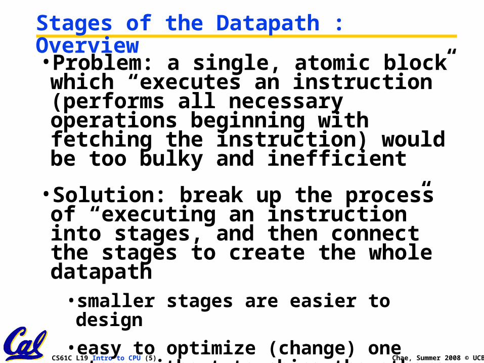
Stages of the Datapath : Overview
• Problem: a single, atomic block which “executes an instruction” (performs all necessary operations beginning with fetching the instruction) would be too bulky and inefficient
• Solution: break up the process of “executing an instruction” into stages, and then connect the stages to create the whole datapath
• smaller stages are easier to design
• easy to optimize (change) one stage without touching the others
CS61C L19 Intro to CPU (6) Chae, Summer 2008 © UCB
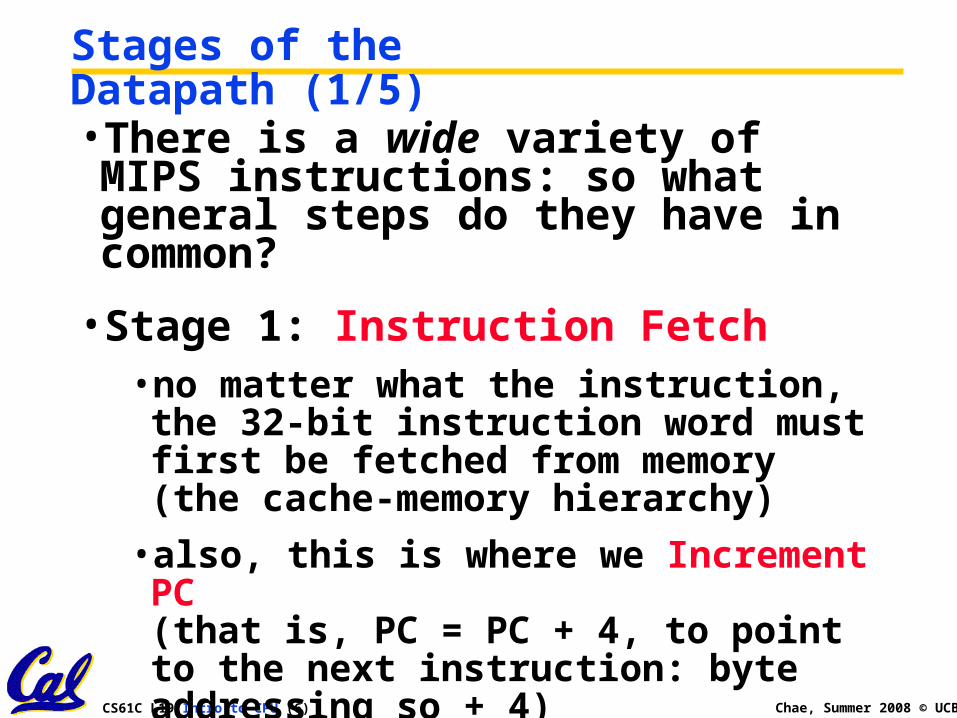
Stages of the Datapath (1/5)
• There is a wide variety of MIPS instructions: so what general steps do they have in common?
• Stage 1: Instruction Fetch• no matter what the instruction, the 32-bit instruction word must first be fetched from memory (the cache-memory hierarchy)
• also, this is where we Increment PC (that is, PC = PC + 4, to point to the next instruction: byte addressing so + 4)

CS61C L19 Intro to CPU (7) Chae, Summer 2008 © UCB
Stages of the Datapath (2/5)
• Stage 2: Instruction Decode• upon fetching the instruction, we next gather data from the fields (decode all necessary instruction data)
• first, read the Opcode to determine instruction type and field lengths
• second, read in data from all necessary registers
- for add, read two registers
- for addi, read one register
- for jal, no reads necessary
CS61C L19 Intro to CPU (8) Chae, Summer 2008 © UCB
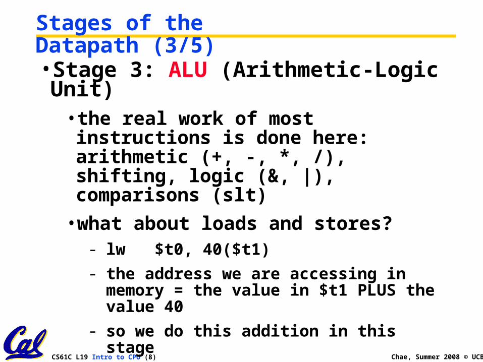
Stages of the Datapath (3/5)
• Stage 3: ALU (Arithmetic-Logic Unit)• the real work of most instructions is done here: arithmetic (+, -, *, /), shifting, logic (&, |), comparisons (slt)
• what about loads and stores?- lw $t0, 40($t1)
- the address we are accessing in memory = the value in $t1 PLUS the value 40
- so we do this addition in this stage

CS61C L19 Intro to CPU (9) Chae, Summer 2008 © UCB
Stages of the Datapath (4/5)
• Stage 4: Memory Access• actually only the load and store instructions do anything during this stage; the others remain idle during this stage or skip it all together
• since these instructions have a unique step, we need this extra stage to account for them
• as a result of the cache system, this stage is expected to be fast
CS61C L19 Intro to CPU (10) Chae, Summer 2008 © UCB
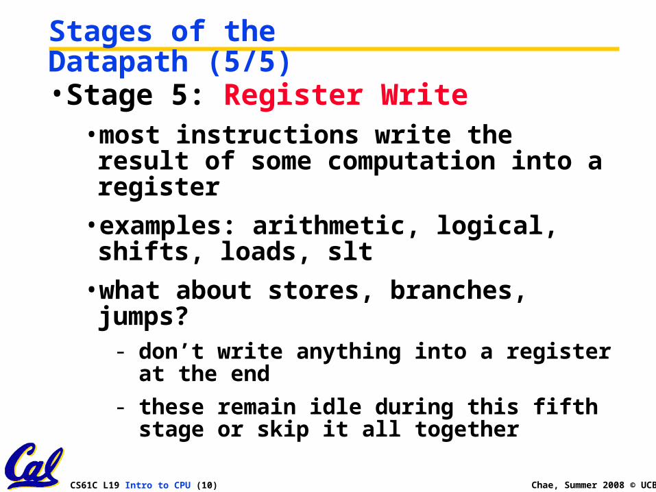
Stages of the Datapath (5/5)
• Stage 5: Register Write• most instructions write the result of some computation into a register
• examples: arithmetic, logical, shifts, loads, slt
• what about stores, branches, jumps?- don’t write anything into a register at the end
- these remain idle during this fifth stage or skip it all together
CS61C L19 Intro to CPU (11) Chae, Summer 2008 © UCB
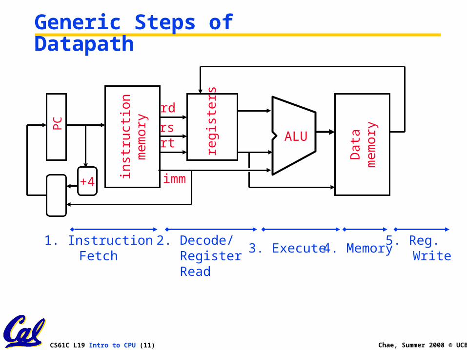
Generic Steps of Datapath
PC
inst
ruct
ion
me
mor
y
+4
rtrs
rd
regi
ste
rs
ALU
Da
tam
em
ory
imm
1. InstructionFetch
2. Decode/ Register
Read
3. Execute 4. Memory5. Reg. Write

CS61C L19 Intro to CPU (12) Chae, Summer 2008 © UCB
Peer Instruction
A. Our ALU is a synchronous device
B. We should use the main ALU to compute PC=PC+4
C. The ALU is inactive for memory reads or writes.
ABC1: FFF2: FFT3: FTF4: FTT5: TFF6: TFT7: TTF8: TTT

CS61C L19 Intro to CPU (13) Chae, Summer 2008 © UCB
Administrivia
• HW4 Due Friday 7/25• Cut out problem 8
• Complaints about HW1 and 2• Submit by Friday or we won’t look at it
• Don’t unplug stuff in the labs!
CS61C L19 Intro to CPU (14) Chae, Summer 2008 © UCB
Administrivia
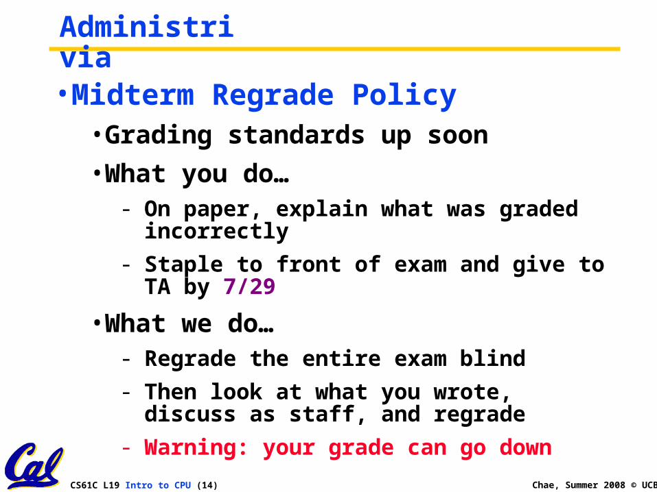
• Midterm Regrade Policy• Grading standards up soon
• What you do…- On paper, explain what was graded
incorrectly
- Staple to front of exam and give to TA by 7/29
• What we do…- Regrade the entire exam blind
- Then look at what you wrote, discuss as staff, and regrade
- Warning: your grade can go down

CS61C L19 Intro to CPU (15) Chae, Summer 2008 © UCB
What does it mean to “clobber” midterm?
• You STILL have to take the final even if you aced the midterm!
• The final will contain midterm-material Qs and new, post-midterm Qs
• They will be graded separately
• If you do “better” on the midterm-material, we will clobber your midterm with the “new” score! If you do worse, midterm unchanged.
• What does “better” mean?• Better w.r.t. Standard Deviations around mean
• What does “new” mean?• Score based on remapping St. Dev. score on
final midterm-material to midterm score St. Dev.
CS61C L19 Intro to CPU (16) Chae, Summer 2008 © UCB
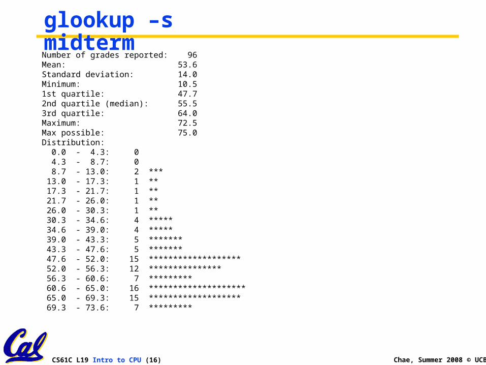
glookup –s midtermNumber of grades reported: 96Mean: 53.6Standard deviation: 14.0Minimum: 10.51st quartile: 47.72nd quartile (median): 55.53rd quartile: 64.0Maximum: 72.5Max possible: 75.0Distribution: 0.0 - 4.3: 0 4.3 - 8.7: 0 8.7 - 13.0: 2 *** 13.0 - 17.3: 1 ** 17.3 - 21.7: 1 ** 21.7 - 26.0: 1 ** 26.0 - 30.3: 1 ** 30.3 - 34.6: 4 ***** 34.6 - 39.0: 4 ***** 39.0 - 43.3: 5 ******* 43.3 - 47.6: 5 ******* 47.6 - 52.0: 15 ******************* 52.0 - 56.3: 12 *************** 56.3 - 60.6: 7 ********* 60.6 - 65.0: 16 ******************** 65.0 - 69.3: 15 ******************* 69.3 - 73.6: 7 *********
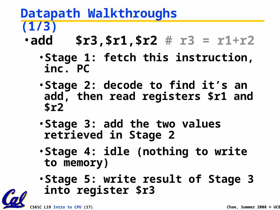
CS61C L19 Intro to CPU (17) Chae, Summer 2008 © UCB
Datapath Walkthroughs (1/3)
•add $r3,$r1,$r2 # r3 = r1+r2• Stage 1: fetch this instruction, inc. PC
• Stage 2: decode to find it’s an add, then read registers $r1 and $r2
• Stage 3: add the two values retrieved in Stage 2
• Stage 4: idle (nothing to write to memory)
• Stage 5: write result of Stage 3 into register $r3

CS61C L19 Intro to CPU (18) Chae, Summer 2008 © UCB
Example: add Instruction
PC
inst
ruct
ion
me
mor
y
+4
regi
ste
rs
ALU
Da
tam
em
ory
imm
2
1
3
add
r3
, r1
, r2
reg[1]+reg[2]
reg[2]
reg[1]
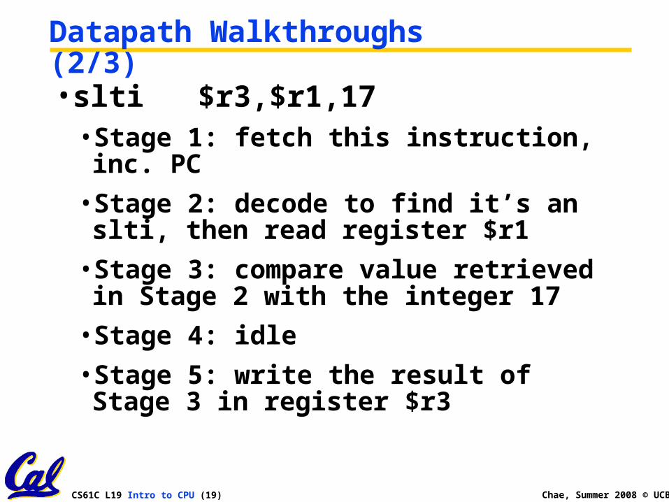
CS61C L19 Intro to CPU (19) Chae, Summer 2008 © UCB
Datapath Walkthroughs (2/3)
•slti $r3,$r1,17• Stage 1: fetch this instruction, inc. PC
• Stage 2: decode to find it’s an slti, then read register $r1
• Stage 3: compare value retrieved in Stage 2 with the integer 17
• Stage 4: idle
• Stage 5: write the result of Stage 3 in register $r3
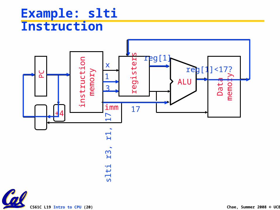
CS61C L19 Intro to CPU (20) Chae, Summer 2008 © UCB
Example: slti Instruction
PC
inst
ruct
ion
me
mor
y
+4
regi
ste
rs
ALU
Da
tam
em
ory
imm
3
1
x
slti
r3, r
1, 1
7
reg[1]<17?
17
reg[1]

CS61C L19 Intro to CPU (21) Chae, Summer 2008 © UCB
Datapath Walkthroughs (3/3)
•sw $r3, 17($r1)• Stage 1: fetch this instruction, inc. PC
• Stage 2: decode to find it’s a sw, then read registers $r1 and $r3
• Stage 3: add 17 to value in register $41 (retrieved in Stage 2)
• Stage 4: write value in register $r3 (retrieved in Stage 2) into memory address computed in Stage 3
• Stage 5: idle (nothing to write into a register)
CS61C L19 Intro to CPU (22) Chae, Summer 2008 © UCB
Example: sw Instruction
PC
inst
ruct
ion
me
mor
y
+4
regi
ste
rs
ALU
Da
tam
em
ory
imm
3
1
x
SW
r3,
17
(r1
)
reg[1]+17
17
reg[1]
ME
M[r
1+1
7]<
=r3
reg[3]

CS61C L19 Intro to CPU (23) Chae, Summer 2008 © UCB
Why Five Stages? (1/2)• Could we have a different number of stages?
• Yes, and other architectures do
• So why does MIPS have five if instructions tend to idle for at least one stage?
• The five stages are the union of all the operations needed by all the instructions.
• There is one instruction that uses all five stages: the load

CS61C L19 Intro to CPU (24) Chae, Summer 2008 © UCB
Why Five Stages? (2/2)•lw $r3, 17($r1)
• Stage 1: fetch this instruction, inc. PC
• Stage 2: decode to find it’s a lw, then read register $r1
• Stage 3: add 17 to value in register $r1 (retrieved in Stage 2)
• Stage 4: read value from memory address compute in Stage 3
• Stage 5: write value found in Stage 4 into register $r3

CS61C L19 Intro to CPU (25) Chae, Summer 2008 © UCB
Example: lw Instruction
PC
inst
ruct
ion
me
mor
y
+4
regi
ste
rs
ALU
Da
tam
em
ory
imm
3
1
x
LW
r3
, 17
(r1
)
reg[1]+17
17
reg[1]
ME
M[r
1+1
7]

CS61C L19 Intro to CPU (26) Chae, Summer 2008 © UCB
Datapath Summary• The datapath based on data transfers required to perform instructions
• A controller causes the right transfers to happen
PC
inst
ruct
ion
me
mor
y
+4
rtrs
rd
regi
ste
rs
ALU
Da
tam
em
ory
imm
Controller
opcode, funct

CS61C L19 Intro to CPU (27) Chae, Summer 2008 © UCB
CPU clocking (1/2)
• Single Cycle CPU: All stages of an instruction are completed within one long clock cycle.
• The clock cycle is made sufficient long to allow each instruction to complete all stages without interruption and within one cycle.
For each instruction, how do we control the flow of information though the datapath?
1. InstructionFetch
2. Decode/ Register
Read
3. Execute 4. Memory5. Reg. Write

CS61C L19 Intro to CPU (28) Chae, Summer 2008 © UCB
CPU clocking (2/2)
• Multiple-cycle CPU: Only one stage of instruction per clock cycle.
• The clock is made as long as the slowest stage.
Several significant advantages over single cycle execution: Unused stages in a particular instruction can be skipped OR instructions can be pipelined (overlapped).
For each instruction, how do we control the flow of information though the datapath?
1. InstructionFetch
2. Decode/ Register
Read
3. Execute 4. Memory5. Reg. Write

CS61C L19 Intro to CPU (29) Chae, Summer 2008 © UCB
How to Design a Processor: step-by-step• 1. Analyze instruction set architecture (ISA)
datapath requirements• meaning of each instruction is given by the register transfers
• datapath must include storage element for ISA registers
• datapath must support each register transfer• 2. Select set of datapath components and establish clocking methodology
• 3. Assemble datapath meeting requirements• 4. Analyze implementation of each instruction to determine setting of control points that effects the register transfer.
• 5. Assemble the control logic (hard part!)

CS61C L19 Intro to CPU (30) Chae, Summer 2008 © UCB
Review: The MIPS Instruction Formats• All MIPS instructions are 32 bits long. 3 formats:
• R-type
• I-type
• J-type
• The different fields are:• op: operation (“opcode”) of the instruction• rs, rt, rd: the source and destination register specifiers• shamt: shift amount• funct: selects the variant of the operation in the “op”
field• address / immediate: address offset or immediate value• target address: target address of jump instruction
op target address
02631
6 bits 26 bits
op rs rt rd shamt funct
061116212631
6 bits 6 bits5 bits5 bits5 bits5 bits
op rs rt address/immediate
016212631
6 bits 16 bits5 bits5 bits

CS61C L19 Intro to CPU (31) Chae, Summer 2008 © UCB
Step 1a: The MIPS-lite Subset for today
• ADDU and SUBU•addu rd,rs,rt•subu rd,rs,rt
• OR Immediate:•ori rt,rs,imm16
• LOAD and STORE Word•lw rt,rs,imm16•sw rt,rs,imm16
• BRANCH:•beq rs,rt,imm16
op rs rt rd shamt funct
061116212631
6 bits 6 bits5 bits5 bits5 bits5 bits
op rs rt immediate
016212631
6 bits 16 bits5 bits5 bits
op rs rt immediate
016212631
6 bits 16 bits5 bits5 bits
op rs rt immediate
016212631
6 bits 16 bits5 bits5 bits

CS61C L19 Intro to CPU (32) Chae, Summer 2008 © UCB
Register Transfer Language• RTL gives the meaning of the instructions
• All start by fetching the instruction
{op , rs , rt , rd , shamt , funct} MEM[ PC ]
{op , rs , rt , Imm16} MEM[ PC ]
inst Register Transfers
ADDU R[rd] R[rs] + R[rt]; PC PC + 4
SUBU R[rd] R[rs] – R[rt]; PC PC + 4
ORI R[rt] R[rs] | zero_ext(Imm16); PC PC + 4
LOAD R[rt] MEM[ R[rs] + sign_ext(Imm16)]; PC PC + 4
STORE MEM[ R[rs] + sign_ext(Imm16) ] R[rt]; PC PC + 4
BEQ if ( R[rs] == R[rt] ) then PC PC + 4 + (sign_ext(Imm16) || 00) else PC PC + 4
CS61C L19 Intro to CPU (33) Chae, Summer 2008 © UCB
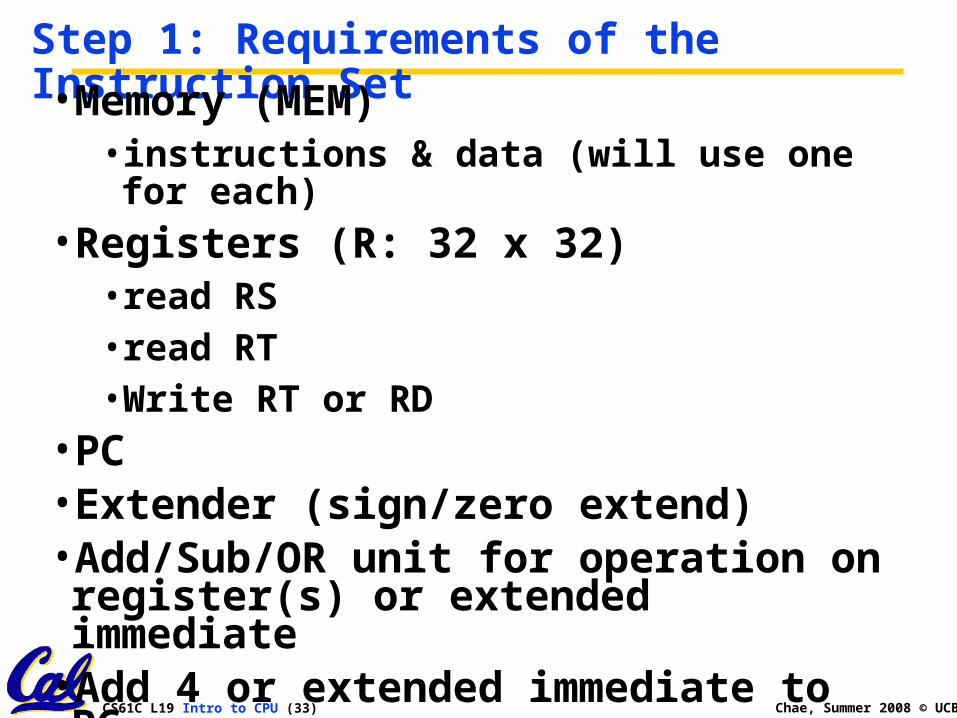
Step 1: Requirements of the Instruction Set• Memory (MEM)
• instructions & data (will use one for each)• Registers (R: 32 x 32)
• read RS• read RT• Write RT or RD
• PC• Extender (sign/zero extend)• Add/Sub/OR unit for operation on register(s) or extended immediate
• Add 4 or extended immediate to PC• Compare registers?

CS61C L19 Intro to CPU (34) Chae, Summer 2008 © UCB
Step 2: Components of the Datapath•Combinational Elements
•Storage Elements• Clocking methodology
CS61C L19 Intro to CPU (35) Chae, Summer 2008 © UCB
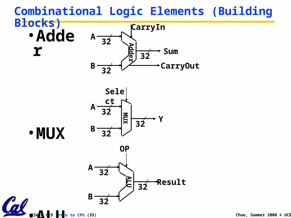
Combinational Logic Elements (Building Blocks)
•Adder
•MUX
•ALU
32
32
A
B32
Sum
CarryOut
32
32
A
B32
Result
OP
32A
B32
Y32
Select
Ad
der
MU
XA
LU
CarryIn

CS61C L19 Intro to CPU (36) Chae, Summer 2008 © UCB
ALU Needs for MIPS-lite + Rest of MIPS• Addition, subtraction, logical OR, ==:
ADDU R[rd] = R[rs] + R[rt]; ...
SUBU R[rd] = R[rs] – R[rt]; ...
ORI R[rt] = R[rs] | zero_ext(Imm16)...
BEQ if ( R[rs] == R[rt] )...
• Test to see if output == 0 for any ALU operation gives == test. How?
• P&H also adds AND, Set Less Than (1 if A < B, 0 otherwise)
• ALU follows chap 5

CS61C L19 Intro to CPU (37) Chae, Summer 2008 © UCB
What Hardware Is Needed? (1/2)• PC: a register which keeps track of memory addr of the next instruction
• General Purpose Registers• used in Stages 2 (Read) and 5 (Write)
• MIPS has 32 of these
• Memory• used in Stages 1 (Fetch) and 4 (R/W)
• cache system makes these two stages as fast as the others, on average

CS61C L19 Intro to CPU (38) Chae, Summer 2008 © UCB
What Hardware Is Needed? (2/2)• ALU
• used in Stage 3• something that performs all necessary functions: arithmetic, logicals, etc.
• we’ll design details later
• Miscellaneous Registers• In implementations with only one stage per clock cycle, registers are inserted between stages to hold intermediate data and control signals as they travels from stage to stage.
• Note: Register is a general purpose term meaning something that stores bits. Not all registers are in the “register file”.

CS61C L19 Intro to CPU (39) Chae, Summer 2008 © UCB
Storage Element: Idealized Memory
• Memory (idealized)• One input bus: Data In• One output bus: Data Out
• Memory word is selected by:• Address selects the word to put on Data Out• Write Enable = 1: address selects the memory
word to be written via the Data In bus• Clock input (CLK)
• The CLK input is a factor ONLY during write operation
• During read operation, behaves as a combinational logic block:
- Address valid Data Out valid after “access time.”
Clk
Data In
Write Enable
32 32DataOut
Address

CS61C L19 Intro to CPU (40) Chae, Summer 2008 © UCB
Storage Element: Register (Building Block)
• Similar to D Flip Flop except- N-bit input and output
- Write Enable input
• Write Enable:- negated (or deasserted) (0):
Data Out will not change
- asserted (1): Data Out will become Data In on positive edge of clock
clk
Data In
Write Enable
N N
Data Out
CS61C L19 Intro to CPU (41) Chae, Summer 2008 © UCB
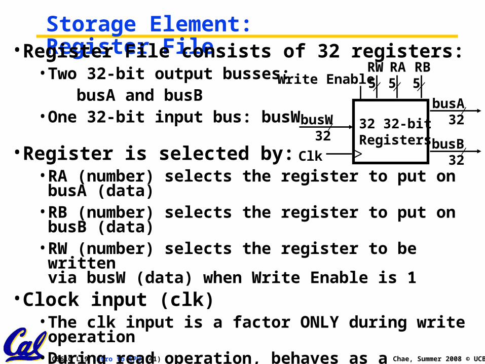
Storage Element: Register File• Register File consists of 32 registers:
• Two 32-bit output busses: busA and busB• One 32-bit input bus: busW
• Register is selected by:• RA (number) selects the register to put on busA (data)• RB (number) selects the register to put on busB (data)• RW (number) selects the register to be written
via busW (data) when Write Enable is 1• Clock input (clk)
• The clk input is a factor ONLY during write operation• During read operation, behaves as a combinational
logic block:- RA or RB valid busA or busB valid after “access time.”
Clk
busW
Write Enable
3232
busA
32busB
5 5 5RWRA RB
32 32-bitRegisters

CS61C L19 Intro to CPU (42) Chae, Summer 2008 © UCB
Peer Instruction
A. If the destination reg is the same as the source reg, we could compute the incorrect value!
B. We’re going to be able to read 2 registers and write a 3rd in 1 cycle
C. Datapath is hard, Control is easy
ABC0: FFF1: FFT2: FTF3: FTT4: TFF5: TFT6: TTF7: TTT

CS61C L19 Intro to CPU (43) Chae, Summer 2008 © UCB
“And In conclusion…”• CPU design involves Datapath,Control
• Datapath in MIPS involves 5 CPU stages
1) Instruction Fetch
2) Instruction Decode & Register Read
3) ALU (Execute)
4) Memory
5) Register Write