Embed Size (px)
Citation preview

CS 61C: Great Ideas in Computer Architecture (Machine Structures)
Lecture 28: Single-Cycle CPUDatapath Control Part 1
Guest Lecturer: Sagar Karandikarhttp://inst.eecs.berkeley.edu/~cs61c/

Technology In the Newshttp://research.microsoft.com/apps/pubs/default.aspx?id=212001
FPGAs are “programmable” hardware used by computer architects and digital circuit designers, lie somewhere between CPUs and custom chips (ASICs).
“Microsoft published a paper at ISCA about using FPGAs in datacenters
Microsoft “Catapult”, ISCA 2014
for page ranking processing for Bing. In a test deployment, MS reported up to 95% more throughput for only 10% more power. The added TCO was less than 30%. Microsoft used Altera Stratix V FPGAs in a PCIe form-factor with 8GB of DDR3 RAM on each board. The FPGAs were connected using a 10Gb SAS network.” - AnandTech
Review
• CPU design involves Datapath, Control– 5 Stages for MIPS Instructions
1. Instruction Fetch2. Instruction Decode & Register Read3. ALU (Execute)4. Memory5. Register Write
• Datapath timing: single long clock cycle or one short clock cycle per stage

Datapath and Control• Datapath based on data transfers required to perform
instructions• Controller causes the right transfers to happen
PC
inst
ruct
ion
me
mor
y
+4
rtrs
rd
regi
ste
rs
Da
tam
em
ory
imm
ALU
Controller
opcode, funct== zero

CPU Clocking (1/2)
• For each instruction, how do we control the flow of information though the datapath?
• Single Cycle CPU: All stages of an instruction completed within one long clock cycle– Clock cycle sufficiently long to allow each instruction to
complete all stages without interruption within one cycle
1. InstructionFetch
2. Decode/ Register
Read
3. Execute 4. Memory5. Reg. Write

CPU Clocking (2/2)
• Alternative multiple-cycle CPU: only one stage of instruction per clock cycle– Clock is made as long as the slowest stage
– Several significant advantages over single cycle execution: Unused stages in a particular instruction can be skipped OR instructions can be pipelined (overlapped)
1. InstructionFetch
2. Decode/ Register
Read
3. Execute 4. Memory 5. Register Write
Agenda
• Stages of the Datapath• Datapath Instruction Walkthroughs• Datapath Design
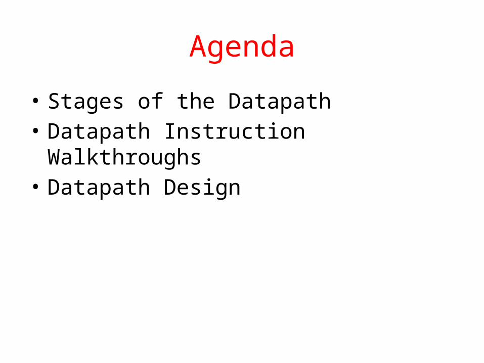
Five Components of a Computer
Processo
r
Computer
Control
Datapath
Memory(passive)
(where programs, data live
whenrunning)
Devices
Input
Output
Keyboard, Mouse
Display, Printer
Disk (where programs, data live when not running)

Processor Design: 5 stepsStep 1: Analyze instruction set to determine datapath
requirements– Meaning of each instruction is given by register transfers– Datapath must include storage element for ISA registers– Datapath must support each register transferStep 2: Select set of datapath components & establish
clock methodologyStep 3: Assemble datapath components that meet the
requirementsStep 4: Analyze implementation of each instruction to
determine setting of control points that realizes the register transfer
Step 5: Assemble the control logic

• All MIPS instructions are 32 bits long. 3 formats:
– R-type
– I-type
– J-type
• The different fields are:– op: operation (“opcode”) of the instruction– rs, rt, rd: the source and destination register specifiers– shamt: shift amount– funct: selects the variant of the operation in the “op” field– address / immediate: address offset or immediate value– target address: target address of jump instruction
op target address
02631
6 bits 26 bits
op rs rt rd shamt funct
061116212631
6 bits 6 bits5 bits5 bits5 bits5 bits
op rs rt address/immediate
016212631
6 bits 16 bits5 bits5 bits
The MIPS Instruction Formats

• ADDU and SUBU– addu rd,rs,rt– subu rd,rs,rt
• OR Immediate:– ori rt,rs,imm16
• LOAD and STORE Word– lw rt,rs,imm16– sw rt,rs,imm16
• BRANCH:– beq rs,rt,imm16
op rs rt rd shamt funct
061116212631
6 bits 6 bits5 bits5 bits5 bits5 bits
op rs rt immediate
016212631
6 bits 16 bits5 bits5 bits
op rs rt immediate
016212631
6 bits 16 bits5 bits5 bits
op rs rt immediate
016212631
6 bits 16 bits5 bits5 bits
The MIPS-lite Subset

• Colloquially called “Register Transfer Language”• RTL gives the meaning of the instructions• All start by fetching the instruction itself{op , rs , rt , rd , shamt , funct} MEM[ PC ]{op , rs , rt , Imm16} MEM[ PC ]
Inst Register TransfersADDU R[rd] R[rs] + R[rt]; PC PC + 4SUBU R[rd] R[rs] – R[rt]; PC PC + 4ORI R[rt] R[rs] | zero_ext(Imm16); PC PC + 4LOAD R[rt] MEM[ R[rs] + sign_ext(Imm16)]; PC PC + 4STORE MEM[ R[rs] + sign_ext(Imm16) ] R[rt]; PC PC + 4BEQ if ( R[rs] == R[rt] ) PC PC + 4 + {sign_ext(Imm16), 2’b00} else PC PC + 4
Register Transfer Level (RTL)

Step 1: Requirements of the Instruction Set
• Memory (MEM)– Instructions & data (will use one for each)
• Registers (R: 32, 32-bit wide registers)– Read RS– Read RT– Write RT or RD
• Program Counter (PC)• Extender (sign/zero extend)• Add/Sub/OR/etc unit for operation on register(s) or extended
immediate (ALU)• Add 4 (+ maybe extended immediate) to PC• Compare registers?
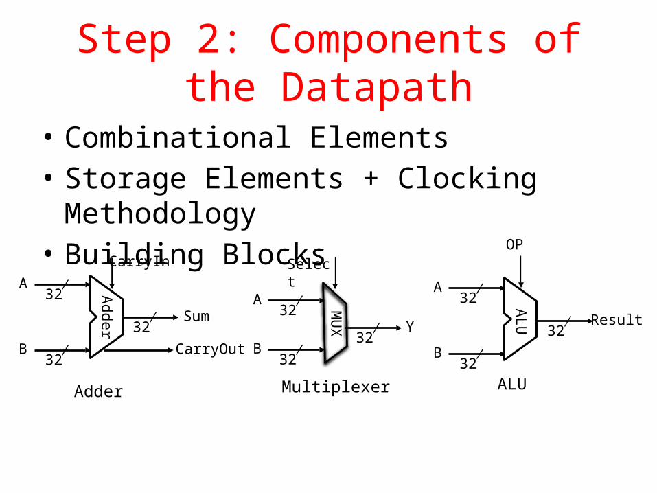
Step 2: Components of the Datapath
• Combinational Elements• Storage Elements + Clocking Methodology• Building Blocks
32
32
A
B32
Sum
CarryOut
CarryIn
Adder
32A
B32
Y32
Select
MU
X
Multiplexer
32
32
A
B32
Result
OP
ALU
ALU
Adder

ALU Needs for MIPS-lite + Rest of MIPS
• Addition, subtraction, logical OR, ==:ADDU R[rd] = R[rs] + R[rt]; ...SUBU R[rd] = R[rs] – R[rt]; ... ORI R[rt] = R[rs] | zero_ext(Imm16)...
BEQ if ( R[rs] == R[rt] )... • Test to see if output == 0 for any ALU
operation gives == test. How?• P&H also adds AND, Set Less Than (1 if A < B, 0
otherwise) • ALU follows Chapter 5
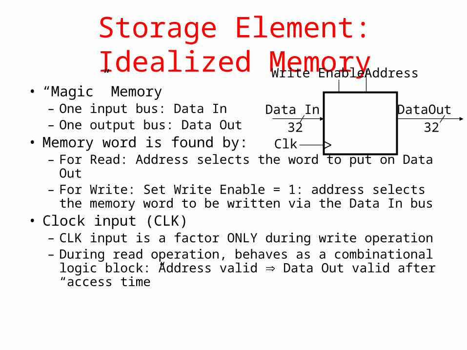
Storage Element: Idealized Memory
• “Magic” Memory– One input bus: Data In– One output bus: Data Out
• Memory word is found by:– For Read: Address selects the word to put on Data Out– For Write: Set Write Enable = 1: address selects the
memory word to be written via the Data In bus• Clock input (CLK)
– CLK input is a factor ONLY during write operation– During read operation, behaves as a combinational logic
block: Address valid Data Out valid after “access time”
Clk
Data In
Write Enable
32 32DataOut
Address

Storage Element: Register (Building Block)
• Similar to D Flip Flop except– N-bit input and output– Write Enable input
• Write Enable:– Negated (or deasserted) (0): Data Out will not
change– Asserted (1): Data Out will become Data In on
positive edge of clock
clk
Data In
Write Enable
N N
Data Out

Storage Element: Register File• Register File consists of 32 registers:
– Two 32-bit output busses:busA and busB
– One 32-bit input bus: busW• Register is selected by:
– RA (number) selects the register to put on busA (data)– RB (number) selects the register to put on busB (data)– RW (number) selects the register to be written
via busW (data) when Write Enable is 1• Clock input (clk)
– Clk input is a factor ONLY during write operation– During read operation, behaves as a combinational logic block:
• RA or RB valid busA or busB valid after “access time.”
Clk
busW
Write Enable
3232
busA
32busB
5 5 5RW RA RB
32 x 32-bitRegisters

Administrivia
• No classes on Tuesday – If you have discussion on Tuesday, go to a M/W discussion.
• Project 3-1 out Sunday– Free to choose new partners, but not forced– Start early!
• Heads Up: No Lab Thanksgiving Week

Step 3a: Instruction Fetch Unit• Register Transfer
Requirements Datapath Assembly
• Instruction Fetch• Read Operands and Execute
Operation• Common RTL operations
– Fetch the Instruction: mem[PC]
– Update the program counter:• Sequential Code:
PC PC + 4 • Branch and Jump:
PC “something else” 32
Instruction WordAddress
InstructionMemory
PCclk
Next AddressLogic

• R[rd] = R[rs] op R[rt] (addu rd,rs,rt)– Ra, Rb, and Rw come from instruction’s Rs, Rt, and Rd fields
– ALUctr and RegWr: control logic after decoding the instruction
• … Already defined the register file & ALU
Step 3b: Add & Subtract
32Result
ALUctr
clk
busW
RegWr
3232
busA
32busB
5 5 5
Rw Ra Rb
32 x 32-bitRegisters
Rs RtRd
ALUop rs rt rd shamt funct
061116212631
6 bits 6 bits5 bits5 bits5 bits5 bits

Clocking Methodology
• Storage elements clocked by same edge• Flip-flops (FFs) and combinational logic have some delays
– Gates: delay from input change to output change – Signals at FF D input must be stable before active clock edge to allow
signal to travel within the FF (set-up time), and we have the usual clock-to-Q delay
• “Critical path” (longest path through logic) determines length of clock period
Clk
.
.
.
.
.
.
.
.
.
.
.
.

Register-Register Timing: One Complete Cycle
Clk
PCRs, Rt, Rd,Op, Func
ALUctr
Instruction Memory Access Time
Old Value New Value
RegWr Old Value New Value
Delay through Control Logic
busA, BRegister File Access Time
Old Value New Value
busWALU Delay
Old Value New Value
Old Value New Value
New ValueOld Value
Register WriteOccurs Here32
ALUctr
clk
busW
RegWr
32busA
32
busB
5 5
Rw Ra Rb
RegFile
Rs Rt
ALU
5Rd
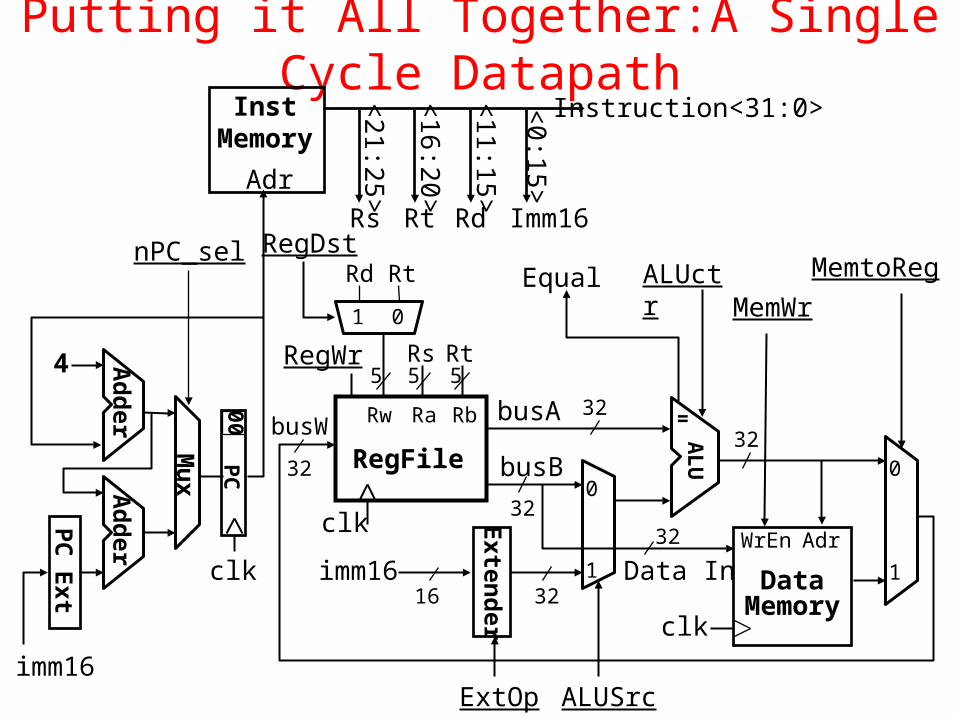
Putting it All Together:A Single Cycle Datapath
imm16
32
ALUctr
clk
busW
RegWr
32
32busA
32
busB
5 5
Rw Ra Rb
RegFile
Rs
Rt
Rt
RdRegDst
Exten
der
3216imm16
ALUSrcExtOp
MemtoReg
clk
Data In32
MemWrEqual
Instruction<31:0><21:25>
<16:20>
<11:15>
<0:15>
Imm16RdRtRs
clk
PC
00
4
nPC_sel
PC
Ext
Adr
InstMemory
Ad
derA
dder
Mu
x
01
0
1
=
AL
U 0
1
WrEn Adr
DataMemory
5

Processor Design: 3 of 5 stepsStep 1: Analyze instruction set to determine datapath
requirements– Meaning of each instruction is given by register transfers– Datapath must include storage element for ISA registers– Datapath must support each register transferStep 2: Select set of datapath components & establish
clock methodologyStep 3: Assemble datapath components that meet the
requirementsStep 4: Analyze implementation of each instruction to
determine setting of control points that realizes the register transfer
Step 5: Assemble the control logic