Embed Size (px)
Citation preview

Corrosion Science, Vol. 28, No. 1, pp. 43-56, 1988 0010-938X/88 $3.00 + 0.00 Printed in Great Britain (~) 1988 Pergamon Journals Ltd.
C R Y S T A L L I Z A T I O N IN A N O D I C O X I D E F I L M S
J. S. L. LEACH and B. R. PEARSON*
Department of Metallurgy and Materials Science, The University of Nottingham, University Park, Nottingham NG7 2RD, U.K.
Abstract--The factors which influence the structure of barrier anodic oxides have been reviewed and it is seen that high internal compressive stresses are conducive to the formation of crystals. These stresses arise when new oxide is formed mainly at the oxide-metal interface and oxygen ion transport dominates the growth process. For some oxides, e.g. Zr02 and HfO~, the oxygen ion transport fraction is close to one at most rates of growth and the anodic oxides are usually crystalline. For others, e.g. A1203, Nb2Os, Ta205 and TiO2, increasing metal ion transport at high rates of growth is associated with the formation of glassy material as the compressive stresses diminish. Incorporation of impurity ions in sufficient quantities may modify the ionic transport fractions and hence the stresses and the degree of crystallinity. Many of the concepts developed for anodic films seem applicable to passive films and oxides grown at high tempera- tures.
I N T R O D U C T I O N
Mosx ENCINEERIN6 metals and alloys oxidize under ambient conditions to form a very thin passive oxide layer, the stability of which in aqueous conditions varies with pH and electrode potential.l
Because they are so thin, passive films are difficult to study directly but thicker films of a similar character may be grown by artificially maintaining the high electric field associated with the formation of thin films, so producing anodically formed or anodic films. 2 These thicker films are of commercial importance as well as scientific interest but there is a limit to the thickness they can achieve without becoming porous, non-adherent or fractured. Such failure is often referred to as breakdown. In anodic films, breakdown is indicated by inability to continue supporting the whole electric field across the thickness, giving rise (under constant-current growth condi- tions) to sudden reductions in voltage and/or in the rate of voltage rise.
The thicker oxide films are of interest because of their dielectric and semi- conducting behaviour which is put to wide use in electronic components such as capacitors 2 and MOS devices. 3 Particularly, the oxide films on Ta, AI, Nb, Zr, Ti, Ge and Si have been investigated extensively with respect to their electrical and optical properties. Generally the anodic oxides are not crystalline (with the notable excep- tions of ZrO2 and HfO2) and the presence of crystalline material (Figs 1 and 2) may impair their electrical and corrosion-resisting properties. Thus the reasons for growth of crystalline material are of commercial and scientific interest.
THE O C C U R R E N C E OF C R Y S T A L L I N E O X I D E
The development of crystalline oxide in those films which are normally amorph- ous (A1203, Ta2Os, Nb2Os, TiO2) can be encouraged artifically. For example, high
* Present address: ICI Paints Division, Wexham Road, Slough SL2 5DS, U.K. Manuscript received 1 January 1987.
43

44 J.S.L. LEACH and B. R. PEARSON
temperatures cause crystallization and in an electron microscope sufficient energy can be absorbed from the electron beam to raise the sample temperature and produce crystals 4'5 (Fig. 3). Crystallization is slower in the presence of impurities. 6'7 This may be because impurities are more easily tolerated by glassy materials than by crystals and consequently, to obtain crystals, longer range diffusion is required rather than a simple local rearrangement. In anodic films, impurities from the electrolyte present in the outer layers have been associated with the slower crystallization of the glassy material. 6'7 The crystalline material then develops from the glass by thermally activated crystallization, most readily at the inner interface where the impurity levels are lower (Fig. 4). This is also observed with metals in which amorphous or glassy structures may be retained after super-rapid quenching from the melt only in the presence of high concentrations of alloying elements, whilst pure metals do not remain glassy.S
Recrystallization of amorphous anodic oxides at the point of their breakdown has also been reported. 9'~° Here, the formation of crystalline material is the result of localized high temperatures occurring at breakdown when large currents flow in limited areas. Crystalline material can form at the outer interface of an anodic oxide, if a dissolution-reprecipitation reaction occurs. This is commonly observed during the growth and sealing of porous AI203 anodic films. 11.12 Crystalline oxide can appear during growth of anodic barrier films when it forms initially at the oxide-metal interface. The anodic oxides of Ta, Nb, AI and Ti can all form glasses and crystals, but normally the anodic oxides of Zr (and Hf) form only crystals. 13'14 Only under certain circumstances has glassy or microcrystalline anodic ZrO2 been observed. 15-1~ Such crystals appearing during anodic growth cannot result from a dissolution- precipitation reaction as they form at the oxide-metal interface. In the case of Ta, the crystals were first thought to be the result of crystallization of the glassy Ta205 at the oxide-metal interface. 2°'2~ However, it has now been suggested that this is new oxide growing at the inner interface 22 (Fig. 5).
An oxide growing at the oxide-metal interface might form crystals due to an epitaxial relationship with the crystalline metal substrate. However, Ta2Os, Nb2Os, AI20 3 and TiO2 oxides grow by anion migration at the oxide-metal interface and simultaneously by cation migration at the oxide-liquid interface. 23'24 In most cases, especially for AI and Ta, and in some cases for Ti, the occurrence of crystalline oxide is restricted to special conditions. In T a 2 0 5 for example, Vermilyea 2°'21 and Jackson 22
reported the appearance of crystalline material in otherwise glassy films only when the current was allowed to fall to a low value under constant voltage growth conditions. Crystal nucleation was thus seen to be associated with the lowest growth rates. Similarly, the crystallization of Nb205 has been reported. 2'25 For glassy AI203 films, Khan 26 showed that crystals formed only when the current was allowed to fall (Fig. 6). Sidgwick 27 studied TiO2 films grown under constant-current conditions. At low current densities (=1-2 mAcm -2) the oxides were crystalline at all thicknesses (Fig. 7). At higher growth rates, the appearance of crystalline oxide was delayed to higher thicknesses, typically 40 nm at 5 mA cm -2 (Fig. 8). Using reflection electron diffraction he showed that the crystals appeared firstly at the metal-oxide interface reaching the oxide-liquid interface only after prolonged oxidation (Fig. 9).
The appearance of crystalline material at the inner interface of otherwise amorphous oxides, which is associated with low growth current densities, excludes the possibility of thermally induced crystallization, as internal power dissipation in

FIG. 1. (Mag. × 19200.) Transmission electron micrograph of an A1203 film grown to 250 V, showing growth of crystallites above grain boundaries. 26 Electropolished substrate.
Electrolyte: 30 g 1 -j pH 9 ammonium borate. 1 mA cm 2.10 min at voltage.
FIG. 2. General transmission electron diffraction pattern from a 300 V AI:O3 film. Electropolished substrate. 26 Electrolyte: 30 g 1-1 pH 9 ammonium borate. 1 mA cm 2.
10 min at voltage.
45

(a) g~Ztlm,
[] Co) . . . . . . . . . . . . . . . .
FIG. 3. Transmission electron micrograph of an ultramicrotomed section of a detached AI203 barrier film formed at a constant current density of 0.5 mA cm -2 on superpure Al at 298 K to 320 V without current decay and subsequently exposed to the electron beam for various times: 6 (a) examined immediately; (b) after 8 min exposure; (c) after 10 min exposure; (d) displaced aperture image of (c) showing the relatively sharp boundary
between the differently textured regions.
' O, l )Jm
FIG. 4. Transmission electron micrograph of the aluminium substrate and its anodic film formed according to the condition of Fig. 3 and exposed to the electron beam for 15 min. 6
46

FIG. 6. (Mag. x 3750.) Transmission electron micrograph of 250 V anodic Al203 film formed on an electropolished aluminium specimen, showing enhanced growth of crystallites at the sites corresponding to the original grain boundaries of the metal. 26 Electrolyte:
30 g 1 -I pH 9 ammonium borate. 1 mA cm 2.10 min at voltage.
Fro. 7. Transmission diffraction pattern from a TiO 2 film grown in 1.88 M H2SO a at applied current density of 1 mA cm 2 at a temperature of 40°C to a potential of 5 V. 27
47

FI6.8. (Mag. x 3500.) Transmission electron micrograph of a TiO2 film grown in 1.88 M H2SO4 at constant applied current density of 5 mA cm -2 to a potential of 20.5 V (=45 nm). 27
FIG. 9. A typical glancing angle electron reflection diffraction pattern from a TiO2 film formed at an applied current density of 5 mA cm -~ in 1.88 M H2504, showing the first
appearance of crystals at the outer interface .27
48

Fx6.12. (Mag. × 1 0 0 . ) G e n e r a l d i s r u p t i o n o f a Z r O 2 f i l m f o r m e d a t 0 . 0 1 m A c m - 2 t o 2 0 0 V in a pH 9 ammon i um borate electrolyte 4o
FIG. 13. (Mag. x 1000.) Blistering in a Z rO 2 film formed at 0.01 m A cm 2 to 200 V in a pH 9 a m m o n i u m borate electrolyte.3~
49

t l i
((3) 5 V Zr02 f i lm from u chemicaLLy etched surface
I0 V ZrO 2 films
from o
( b ) ChemicaLLy ~, etched sur face
( e ) e lec t ro polished surface
o ~ Q 0
( C ) 20 V ZrO 2 f i lm from a chemicaLLy
etched surface
( d ) :50 V ZrO 2 f i lm
from a chemicaLLy
etched surface
FIG. 17. Transmission electron diffraction patterns produced from Z r O 2 films stripped from chemically etched (a~t) and electropolished (e) Zr surfaces. Different oxide thick-
~4 nesses are shown. 5 Electrolyte: pH 9 ammonium borate.
50

Crystallization in anodic oxide films 51
o ;...: ' ,~ • ' . . 7 , . . ~ - , - - - . - . - - - . . _Amorphous ox, e T4000; . o,,,,
} " \ " ' ' - - < I i . . ' i . . . " . .:" ~Tontolu m ,
FIG. 5. Schematic diagram of crystalline Ta20~ growth. Thicknesses relate to anodization in 2% HNO3 at 120 V. (85°C, 60 min, constant voltage.) 22
the oxides is low and provided there is no breakdown producing local high tempera- tures, the mean oxide temperature remains low 28-31 (Fig. 10). That ZrO2 and HfO2 are unusual for growth almost exclusively by transport of oxygen ions 23'24'32-34 and for their crystalline state during anodic oxidation13'14 suggests that the appearance of crystalline material during the growth of barrier oxides is associated with the anion solid-state diffusion mechanism. Thus, if formed as a result of oxygen ion transport, crystalline material must be confined to the inner interface where it is formed under constraint both from the existing oxide and from the substrate metal. Constraint is, however, not a sufficient criterion, for although about 0,7-0.8 of Ta205 and Nb2Os, 0.3--0.7 of anodic AI203 and 0,6--0.7 of anodic TiO2 is formed at the inner oxide surface 32, these oxides are normally free from crystals except at low growth rates. Stringer 35 and Saunders 36 have discussed those mechanisms which give rise to stresses in oxides and it is now widely accepted that the most important is associated with the volume change accompanying the oxidation of the metal (i.e. the Pilling- Bedworth ratio37),
For ZrO2 and HfO2 with Pilling-Bedworth ratios of 1.52 and 1.48, respectively 23 and oxygen-ion transport numbers close to unity 23'24'32-34 it is not surprising that the stresses are normally highly compressive, reaching their highest levels at low growth
6 0 - ? tO 04
50- -
O e o 4o
o o 830
2 0 . - 8 o
o o
E I 0 ' - o
.~_
0 20 4 0 6 0 BO I00 120 140 160 180
C u r r e n t d e n s i t y ( r n A crn 2)
FiG. 10. T e m p e r a t u r e rise in a n AI wire as a f u n c t i o n o f c o n s t a n t a n o d i z i n g c u r r e n t
dens i ty . 2~ 9 9 . 9 9 9 % AI wire . E l ec t ro ly t e : p H 9 .7 a m m o n i u m b o r a t e .

52 J.S.L. LEACH and B. R. PEARSON
15,000
pH9 ammonium bomt~
10,00C
,o
~ 5,ooo
0
0 I I
0-01 0"1 1-0 10-0
Applied currenf dmsify (mA.cm-2)
FIG. 1 l. Internal stress vs growth rate for 180 V ZrO 2 films formed in pH 9 ammonium borate electrolyte at constant current density. 39
rates 34'38'39 (Fig. 11). In thick ZrO2 films grown slowly, the compressive stresses are high enough to cause mechanical failure 39,4° (Figs 12 and 13). Increasing the growth rate reduces the compressive stresses but they are always large at current densities below 50 mA cm-2.
In other oxides, the magnitude of stresses is sensitive to several factors but most notably growth rate. For example Bradhurst and Leach 41,42 and Breen 43 showed that the magnitude and sign of stresses in anodic AI20 3 are a function of current density,
10p00
pH9 ammonium borate
AI203 barrier films
5,ooo I
5,0001 ~ i 0-01 0.I 1-0 10-0
Fro. 14. Internal stress vs growth rate for AI203 films formed in pH 9 ammonium borate electrolyte. 42

Crystallization in anodic oxide films 53
I O - -
0 9 - -
~ ° . . _ • 0 8 -- ° / ° I0
A 0 . 7 - - o / oo 'E z 0 6 - /
~, o 5 - o
04 / 0 ~ j,,,o." -.o-" 4 0
I c~ • • . . . . m
~ T P " • . . . . . . . . " ' " 02 / ~p .... • " " 6.0 " //.~11. D. ill'' ~ i 0 I .. • ,D- .--43----.o-.--o--'--.s-----o-,--.
"-- 100 o / 0 / i ._ . . . . . . . . . . . . . . . . . . . . .
O3
0 4 1 1 1 I I I I ] I i I I 20 40 60 80 100 120 140 160 180 200
Vottoge V (voLts)
FIG. 15. Stress vs formation voltage for Z rO 2 films formed at different growth rates on chemically etched substrates in pH 10 (0.1 M N a H C O 3 + 0.1 M Na2CO3).
@ A 0.044 M NH4HB407 /
o 8 - I mA cm -2 / o# / "
.- o 06 Zr ~"G hanicaLty end e, ,ro 7 ~o4
/ 02 emicaLLy etched 2
f _m ~ •
0 i0 20 30 Fi t • formotion voltoge (a thickness)
Fie,. 16. The effect of surface preparation upon stresses during the initial formation of ZrO 2 films. 4~ 99.95% Zr (annealed), Electrolyte: pH 8.5 ammonium borate. I mA em -2.

54 J . S . L . LEACH and B. R. PEARSON
TABLE 1. PILLING--BEDWORTH RATIOS FOR CRYSTALLINE AND GLASSY OXIDES
Volume Vo occupied by Calculated Pilling-Bedworth Volume V M occupied by 1 mole of oxide MxOy ratio (q~) x moles of metal in M~O v (cm 3) ~ = Vo/V ~
Metal (cm 3) Crystal Glass Crystal Glass
AI 20.0 25.5-28.3 31.9-34.0 1.3-1.4 1.6-1.7 (Ref. 55) (Ref. 55)
Ta 21.8 52.8-54.0 55.7 2.5 2.6 (Ref. 56) (Ref. 56)
Ti 10.6 19.2-20.8 23.9-25.9 1.9 2.3-2.4 (Ref. 57) (Ref. 57)
Nb 21.7 51.4-58.4 61.0 2.4-2.7 2.8 (Ref. 58) (Ref. 58)
Zr 14.1 21.6 Nodata 1.5 - - (Ref. 59)
Hf 13.4 21.7 No data 1.6 - - (Ref. 60)
being generally small and tensile at growth rates normally used, but becoming large and compressive at very low growth rates (Fig. 14).
Recent studies 3"44"45 of anodic AI20 3 growth at constant current density show that at values of current density above 1 mA cm -2 the oxide is entirely glassy, while at and below about 0.2 mA cm -2 crystals are developing. It is in this range of growth rate that the change from tensile to compressive stress in the oxide was identified. 41'42 This work is in agreement with that carried out previously 26 where the appearance of crystalline material was observed in otherwise amorphous oxides, but only at low growth rates during current decay at constant voltage. Thus it seems that in addition to anion transport, which is present in all the systems considered, it is necessary to have high compressive stresses if crystalline material is to be formed in the oxide during anodic oxidation.
It is possible that stresses may be relieved by allowing deformation by a Herring-Nabarro mechanism. 42'46 However, for this to operate, both ionic species must be mobile and the deformation rate is controlled by the slowest moving s p e c i e s . 47
Unfortunately, detailed information on stresses in Ta205, Nb205 and TiO2 is not readily available, especially as a function of current density. Vermilyea 48 noted that under most circumstances, the internal stresses in Ta205 and Nb205 are tensile, in the amorphous oxides. As in A1203, however, crystals have been observed during current decayY °-22"25 and it is likely that these oxides have similar stress behaviour, going more compressive as the current density falls. In TiO2 the reported data are often contradictory. Some authors 49's°'51 have measured compressive stresses, while others report mostly tensile stresses. 27'48'52 At low current densities Sidgwick 27 showed that TiO 2 films are crystalline but that at higher current densities the initial film is a glass with a crystalline layer developing at the metal--oxide interface.
The influence of impurity ion pickup either from the substrate or the electrolyte upon stresses is important. In a series of experiments 19,38.43.49-54 it has been shown that during the growth of anodic films (particularly ZrO2) on chemically etched and hence F--ion contaminated surfaces, stresses, as measured by the deflection of a bending

Crystallization in anodic oxide films 55
beam, are low and sometimes tensile in the initial stages of growth, when F--ion concentration in the oxide is significant (Fig. 15). These initial low stresses were not seen in oxides grown on mechanically polished or electropolished surfaces which were found to be free from F--ion contamination (Fig. 16). X-ray photo- electron spectroscopy (XPS) techniques have confirmed the presence of F--ion contamination in these ZrO2 films and some transmission electron diffraction results 53'54 (Fig. 17) indicate that glassy or microcrystalline material, rather than fully crystalline material predominates in the low-stress region.
The question then arises as to why compressive stresses should encourage the formation of a crystalline oxide rather than a glass. The amorphous oxides all occupy larger volumes than the same weight of crystalline material (Table 1). The growth of crystalline material will generally be favoured under those conditions when amorphous material would be under compressive stress. In the case of A1203, for which more extensive data exist than for the other oxides, the transition from tensile to compressive stresses occurs at current densities of approximately 0.2 mA cm -2. Above this current density the oxides are amorphous. At lower current densities, when stresses become compressive, crystalline material can be observed.
C O N C L U S I O N S
In otherwise amorphous anodic oxides, crystals may form at the inner interface when neither heating nor precipitation can be responsible. This occurs only when conditions of growth are such as to produce compressive stresses in the oxide. The sign and magnitude of oxide stresses are generally related to growth rate and the stresses become more compressive as the growth rate falls. The oxide on zirconium, which is usually under compression, is crystalline in all but a few special conditions and these are associated with the presence of tensile stresses in the anodic ZrO2 due to impurities. At the current densities and under the experimental conditions normally employed for anodic oxide formation, the oxides on Ta, Nb and Ti are in tension and are glassy in spite of a significant anion transport number. In AI203 the observed change from tensile to compressive stresses, associated with falling current density, is also associated with the first appearance of crystal growth.
R E F E R E N C E S I. M. POURBAIX, Atlas of Electrochemical Equilibria. Pergamon Press. London (1966). 2. L. YOUNC, Anodic Oxide Films. Academic Press, London (1961). 3. K. S. CHARI and B. MATHUR, Thin Solid Films 81,271 (1981). 4. A. ALADJEM, D. G. BRANDON, J. YAHALOM and J. ZAHAVI, Electrochim. Acta 15,663 (1970). 5. P. NEUFELD, N. K. NAGPAUL, R. ASHDOWN and M. AKBAR, Electrochim. Acta 17, 1543 (1972). 6. K. SHIMIZU, G. E. THOMPSON and G. C. WOOD, Thin Solid Films 77,313 (1981). 7. K. SmMlZU, G. E. THOMPSON and G. C. WOOD, Thin Solid Films 85, 53 (1981). 8. H. A. DAVIES, Proc. 3rd Int. Conf. on Rapidly Quenched Metals, University of Sussex, England (July
1978). 9. J. YAHALOM and J. ZAHAVl, Electrochim. Acta 15, 1429 (1970).
10. J. YAHALOM and J. ZAHAVl, Electrochim. Acta 16,603 (1971). 11. G.C. WOOD and J. P. O'SULLIVAN, J. electrochem. Soc. 116, 1351 (1969). 12. M. F. ABD RABBO, J. A. RICHARDSON and G. C. WOOD, Corros. Sci. 16,689 (1976). 13. G. ALESSAND~INI, G. DASSU and R. PERUZZl, Energia Nucleare 16,568 (1969). 14. R.D. MlSCn and W. E. RUTHER, J. electrochem. Soc. 100,531 (1953). 15. A. CHARLESBY, Acta Met. 1,340 (1953).
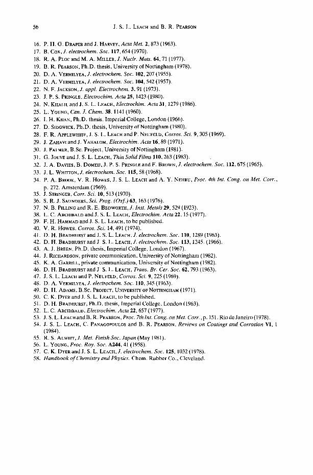
56 J . S . L . LEACH and B. R. PEARSON
16. P. H. G. DRAPER and J. HARVEY, Acla Met. 2,873 (1963). 17. B. Cox, J. electrochem. Soc. 117,654 (1970). 18. R. A. PLOC and M. A. MILLER, J. Nuclr. Mats. 64,71 (1977). 19. B. R. PEARSON, Ph.D. thesis, University of Nottingham (1978). 20. D. A. VERMILYEA, J. electrochem. Soc. 102,207 (1955). 21. D. A. VERMILYEA, J. electrochem. Soc. 104,542 (1957). 22. N.F. JACKSON, J, appl. Electrochem. 3, 91 (1973). 23. J. P. S. PRINGEE, Electrochim. Acta 25, 1423 (1980). 24. N. KHALIL and J. S. L. LEACH, Electrochim. Acta 31, 1279 (1986). 25. L. YOUNG, Can. J. Chem. 38, 1141 (1960). 26. I .H. KHAN, Ph.D. thesis, Imperial College, London (1966). 27. D. SIDGWlCK, Ph.D. thesis, University of Nottingham (1980). 28. F. R. APPLEWHITE, J. S. L. LEACH and P. NEUFELD, Corros. Sci. 9,305 (1969). 29. J. ZAHAVI and J. YAHALOM, Electrochim. Acta 16, 89 (1971). 30. J. PALMER, B.Sc. Project, University of Nottingham (1981). 31. G. JOUVE and J. S. L. LEACH, Thin Solid Films 110,263 (1983). 32. J. A. DAVIES, B. DOMEIJ, J. P. S. PR1NGLE and F. BROWN, J. electrochem. Soc. 112,675 (1965). 33. J. L. WHIYroN, J. electrochem. Soc. 115, 58 (1968). 34. P. A. BROOK, V. R. HOWLS, J. S. L. LEACH and A. Y. NEHRU, Proc. 4th Int. Cong. on Met. Corr.,
p. 272. Amsterdam (1969). 35. J. STRINGER, Corr. Sci. 10,513 (1970). 36. S. R. J. lAUNDERS, Sci. Prog. (Oxf.) 63, 163 (1976). 37. N. B. PILLING and R. E. BEDWORTH, J. Inst. Metals 29,529 (1923). 38. L. C. ARCHIBALD and J. S. L. LEACH, Electrochim. Acta 22, 15 (1977). 39. F. H. HAMMAD and J. S. L. LEACH, to be published. 40. V. R. HOWLS. Corros. Sci. 14,491 (1974). 41. D. H. BRADHURST and J. S. L. LEACH, J. electrochem. Soc. 110, 1289 (1963). 42. D. H. BRADHURST and J. S. L. LEACH, J. electrochem. Soc. 113, 1245. (1966). 43. A. J. BREEN, Ph.D. thesis, Imperial College, London (1967). 44. J. RICHARDSON, private communication, University of Nottingham (1982). 45. K. A. GARRlLL, private communication, University of Nottingham (1982). 46. D. H. BRADHURST and J. S. L. LEACH, Trans. Br. Cer. Soc. 62,793 (1963). 47. J. S. L. LEACH and P. NEUFELD, Corros. Sci. 9,225 (1969). 48. D. A. VERMILYEA, J. electrochem. Soc. 110,345 0963). 49. D. H. ADAMS, B. Sc. PROJECT, UNIVERSITY OF NOTTINGHAM (1971 ). 50. C. K. DYER and J. S. L. LEACH, to be published. 51. D. H. BRADHURST, Ph.D. thesis, Imperial College, London (1963). 52. L. C. ARCHIBALD, Electrochim. Acta 22,657 (1977). 53. J .S.L. LEACH and B. R. PEARSON, Proc. 7th Int. Cong. on Met. Corr., p. 151. Rio de Janeiro (1978). 54. J. S. L. LEACH, C. PANAGOPOULOS and B. R. PEARSON, Reviews on Coatings and Corrosion VI, 1
(1984). 55. R. S. ALWITT, J. Met. Finish Soc. Japan (May 1981). 56. L. YOUNG, Proc. Roy. Soc. A244, 41 0958). 57. C. K. DYER and J. S. L. LEACH, J. electrochem. Soc. 125, 1032 (1978). 58. Handbook of Chemistry and Physics. Chem. Rubber Co., Cleveland.


![Preparation of anodic aluminum oxide (AAO) nano-template …electrolytes under appropriate electrochemical conditions [3-5]. The synthesis and application of nanoporous alumina mask](https://img.dokumen.tips/doc/110x75/60c2ff62b7970f410e08e26b/preparation-of-anodic-aluminum-oxide-aao-nano-template-electrolytes-under-appropriate.jpg)