Embed Size (px)
Citation preview

DOCUMENT NUMBERS12CRGV5/D
F
ree
sca
le S
em
ico
nd
uc
tor,
I
Freescale Semiconductor, Inc.n
c..
.
CRG
Block Guide
V05.04
Original Release Date: 20 November 2003Revised: 26 May 2004
Motorola, Inc.
Motorola reserves the right to make changes without further notice to any products herein to improve reliability, function ordesign. Motorola does not assume any liability arising out of the application or use of any product or circuit described herein;neither does it convey any license under its patent rights nor the rights of others. Motorola products are not designed, intended,or authorized for use as components in systems intended for surgical implant into the body, or other applications intended tosupport or sustain life, or for any other application in which the failure of the Motorola product could create a situation wherepersonal injury or death may occur. Should Buyer purchase or use Motorola products for any such unintended or unauthorizedapplication, Buyer shall indemnify and hold Motorola and its officers, employees, subsidiaries, affiliates, and distributors harmlessagainst all claims, costs, damages, and expenses, and reasonable attorney fees arising out of, directly or indirectly, any claim ofpersonal injury or death associated with such unintended or unauthorized use, even if such claim alleges that Motorola wasnegligent regarding the design or manufacture of the part.
1
For More Information On This Product,
Go to: www.freescale.com

CRG Block Guide — V05.04
Fre
esc
ale
Se
mic
on
du
cto
r, I
Freescale Semiconductor, Inc.n
c..
.
Revision History
VersionNumber
RevisionDate
EffectiveDate Author Description of Changes
V05.00 20 Nov. 03 20 Nov. 03
Initial release for S12X.Added new features (versus S12):Fast wakeup (in self clock mode) from full stopDecimal prescaling for RTIIllegal Address ResetRemoved SYSWAI bit/feature
V05.01 26 Mar. 04 26 Mar. 04 corrected COPCTL register description
V05.02 23 Apr. 04 23 Apr. 04 removed CWAI bit/feature, removed ROAWAI bit/feature
V05.03 14 May 04 14 May 04 improved COPCTL register description
V05.04 26 May 04 26 May 04 REFDV Register description: added REFDV5 and REFDV4 bits
2
For More Information On This Product,
Go to: www.freescale.com

CRG Block Guide — V05.04
Fre
esc
ale
Se
mic
on
du
cto
r, I
Freescale Semiconductor, Inc.n
c..
.
Table of Contents
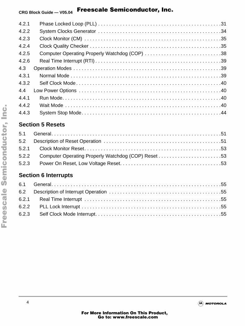
Section 1 Introduction
1.1 Overview. . . . . . . . . . . . . . . . . . . . . . . . . . . . . . . . . . . . . . . . . . . . . . . . . . . . . . . . . . . . . .9
1.2 Features . . . . . . . . . . . . . . . . . . . . . . . . . . . . . . . . . . . . . . . . . . . . . . . . . . . . . . . . . . . . . .9
1.3 Modes of Operation . . . . . . . . . . . . . . . . . . . . . . . . . . . . . . . . . . . . . . . . . . . . . . . . . . . . .9
1.4 Block Diagram . . . . . . . . . . . . . . . . . . . . . . . . . . . . . . . . . . . . . . . . . . . . . . . . . . . . . . . .10
Section 2 Signal Description
2.1 Overview. . . . . . . . . . . . . . . . . . . . . . . . . . . . . . . . . . . . . . . . . . . . . . . . . . . . . . . . . . . . .13
2.2 Detailed Signal Descriptions. . . . . . . . . . . . . . . . . . . . . . . . . . . . . . . . . . . . . . . . . . . . . .13
2.2.1 VDDPLL, VSSPLL . . . . . . . . . . . . . . . . . . . . . . . . . . . . . . . . . . . . . . . . . . . . . . . . . . .13
2.2.2 XFC . . . . . . . . . . . . . . . . . . . . . . . . . . . . . . . . . . . . . . . . . . . . . . . . . . . . . . . . . . . . . .13
2.2.3 RESET . . . . . . . . . . . . . . . . . . . . . . . . . . . . . . . . . . . . . . . . . . . . . . . . . . . . . . . . . . . .13
Section 3 Memory Map and Registers
3.1 Overview. . . . . . . . . . . . . . . . . . . . . . . . . . . . . . . . . . . . . . . . . . . . . . . . . . . . . . . . . . . . .15
3.2 Module Memory Map . . . . . . . . . . . . . . . . . . . . . . . . . . . . . . . . . . . . . . . . . . . . . . . . . . .15
3.3 Register Descriptions . . . . . . . . . . . . . . . . . . . . . . . . . . . . . . . . . . . . . . . . . . . . . . . . . . .15
3.3.1 CRG Synthesizer Register (SYNR) . . . . . . . . . . . . . . . . . . . . . . . . . . . . . . . . . . . . . .15
3.3.2 CRG Reference Divider Register (REFDV) . . . . . . . . . . . . . . . . . . . . . . . . . . . . . . . .16
3.3.3 Reserved Register (CTFLG) . . . . . . . . . . . . . . . . . . . . . . . . . . . . . . . . . . . . . . . . . . .16
3.3.4 CRG Flags Register (CRGFLG). . . . . . . . . . . . . . . . . . . . . . . . . . . . . . . . . . . . . . . . .17
3.3.5 CRG Interrupt Enable Register (CRGINT) . . . . . . . . . . . . . . . . . . . . . . . . . . . . . . . . .18
3.3.6 CRG Clock Select Register (CLKSEL). . . . . . . . . . . . . . . . . . . . . . . . . . . . . . . . . . . .19
3.3.7 CRG PLL Control Register (PLLCTL) . . . . . . . . . . . . . . . . . . . . . . . . . . . . . . . . . . . .21
3.3.8 CRG RTI Control Register (RTICTL) . . . . . . . . . . . . . . . . . . . . . . . . . . . . . . . . . . . . .23
3.3.9 CRG COP Control Register (COPCTL) . . . . . . . . . . . . . . . . . . . . . . . . . . . . . . . . . . .25
3.3.10 Reserved Register (FORBYP) . . . . . . . . . . . . . . . . . . . . . . . . . . . . . . . . . . . . . . . . . .27
3.3.11 Reserved Register (CTCTL) . . . . . . . . . . . . . . . . . . . . . . . . . . . . . . . . . . . . . . . . . . .28
3.3.12 CRG COP Timer Arm/Reset Register (ARMCOP). . . . . . . . . . . . . . . . . . . . . . . . . . .28
Section 4 Functional Description
4.1 General. . . . . . . . . . . . . . . . . . . . . . . . . . . . . . . . . . . . . . . . . . . . . . . . . . . . . . . . . . . . . .31
4.2 Functional Blocks . . . . . . . . . . . . . . . . . . . . . . . . . . . . . . . . . . . . . . . . . . . . . . . . . . . . . .31
3
For More Information On This Product,
Go to: www.freescale.com
CRG Block Guide — V05.04
Fre
esc
ale
Se
mic
on
du
cto
r, I
Freescale Semiconductor, Inc.n
c..
.
4.2.1 Phase Locked Loop (PLL) . . . . . . . . . . . . . . . . . . . . . . . . . . . . . . . . . . . . . . . . . . . . .31
4.2.2 System Clocks Generator . . . . . . . . . . . . . . . . . . . . . . . . . . . . . . . . . . . . . . . . . . . . .34
4.2.3 Clock Monitor (CM) . . . . . . . . . . . . . . . . . . . . . . . . . . . . . . . . . . . . . . . . . . . . . . . . . .35
4.2.4 Clock Quality Checker . . . . . . . . . . . . . . . . . . . . . . . . . . . . . . . . . . . . . . . . . . . . . . . .35
4.2.5 Computer Operating Properly Watchdog (COP) . . . . . . . . . . . . . . . . . . . . . . . . . . . .38
4.2.6 Real Time Interrupt (RTI) . . . . . . . . . . . . . . . . . . . . . . . . . . . . . . . . . . . . . . . . . . . . . .39
4.3 Operation Modes . . . . . . . . . . . . . . . . . . . . . . . . . . . . . . . . . . . . . . . . . . . . . . . . . . . . . .39
4.3.1 Normal Mode . . . . . . . . . . . . . . . . . . . . . . . . . . . . . . . . . . . . . . . . . . . . . . . . . . . . . . .39
4.3.2 Self Clock Mode . . . . . . . . . . . . . . . . . . . . . . . . . . . . . . . . . . . . . . . . . . . . . . . . . . . . .40
4.4 Low Power Options . . . . . . . . . . . . . . . . . . . . . . . . . . . . . . . . . . . . . . . . . . . . . . . . . . . .40
4.4.1 Run Mode. . . . . . . . . . . . . . . . . . . . . . . . . . . . . . . . . . . . . . . . . . . . . . . . . . . . . . . . . .40
4.4.2 Wait Mode . . . . . . . . . . . . . . . . . . . . . . . . . . . . . . . . . . . . . . . . . . . . . . . . . . . . . . . . .40
4.4.3 System Stop Mode. . . . . . . . . . . . . . . . . . . . . . . . . . . . . . . . . . . . . . . . . . . . . . . . . . .44
Section 5 Resets
5.1 General. . . . . . . . . . . . . . . . . . . . . . . . . . . . . . . . . . . . . . . . . . . . . . . . . . . . . . . . . . . . . .51
5.2 Description of Reset Operation . . . . . . . . . . . . . . . . . . . . . . . . . . . . . . . . . . . . . . . . . . .51
5.2.1 Clock Monitor Reset. . . . . . . . . . . . . . . . . . . . . . . . . . . . . . . . . . . . . . . . . . . . . . . . . .53
5.2.2 Computer Operating Properly Watchdog (COP) Reset . . . . . . . . . . . . . . . . . . . . . . .53
5.2.3 Power On Reset, Low Voltage Reset. . . . . . . . . . . . . . . . . . . . . . . . . . . . . . . . . . . . .53
Section 6 Interrupts
6.1 General. . . . . . . . . . . . . . . . . . . . . . . . . . . . . . . . . . . . . . . . . . . . . . . . . . . . . . . . . . . . . .55
6.2 Description of Interrupt Operation . . . . . . . . . . . . . . . . . . . . . . . . . . . . . . . . . . . . . . . . .55
6.2.1 Real Time Interrupt . . . . . . . . . . . . . . . . . . . . . . . . . . . . . . . . . . . . . . . . . . . . . . . . . .55
6.2.2 PLL Lock Interrupt . . . . . . . . . . . . . . . . . . . . . . . . . . . . . . . . . . . . . . . . . . . . . . . . . . .55
6.2.3 Self Clock Mode Interrupt. . . . . . . . . . . . . . . . . . . . . . . . . . . . . . . . . . . . . . . . . . . . . .55
4
For More Information On This Product,
Go to: www.freescale.com

CRG Block Guide — V05.04
Fre
esc
ale
Se
mic
on
du
cto
r, I
Freescale Semiconductor, Inc.n
c..
.
List of Figures
Figure 1-1 Block diagram of CRG. . . . . . . . . . . . . . . . . . . . . . . . . . . . . . . . . . . . . . . . . . . . .11
Figure 2-1 PLL Loop Filter Connections . . . . . . . . . . . . . . . . . . . . . . . . . . . . . . . . . . . . . . . .13
Figure 3-1 CRG Synthesizer Register (SYNR) . . . . . . . . . . . . . . . . . . . . . . . . . . . . . . . . . . .16
Figure 3-2 CRG Reference Divider Register (REFDV) . . . . . . . . . . . . . . . . . . . . . . . . . . . . .16
Figure 3-3 Reserved Register (CTFLG) . . . . . . . . . . . . . . . . . . . . . . . . . . . . . . . . . . . . . . . .17
Figure 3-4 CRG Flags Register (CRGFLG) . . . . . . . . . . . . . . . . . . . . . . . . . . . . . . . . . . . . .17
Figure 3-5 CRG Interrupt Enable Register (CRGINT). . . . . . . . . . . . . . . . . . . . . . . . . . . . . .19
Figure 3-6 CRG Clock Select Register (CLKSEL) . . . . . . . . . . . . . . . . . . . . . . . . . . . . . . . .20
Figure 3-7 CRG PLL Control Register (PLLCTL) . . . . . . . . . . . . . . . . . . . . . . . . . . . . . . . . .21
Figure 3-8 CRG RTI Control Register (RTICTL) . . . . . . . . . . . . . . . . . . . . . . . . . . . . . . . . . .23
Figure 3-9 CRG COP Control Register (COPCTL) . . . . . . . . . . . . . . . . . . . . . . . . . . . . . . . .25
Figure 3-10 Reserved Register (FORBYP). . . . . . . . . . . . . . . . . . . . . . . . . . . . . . . . . . . . . . .27
Figure 3-11 Reserved Register (CTCTL) . . . . . . . . . . . . . . . . . . . . . . . . . . . . . . . . . . . . . . . .28
Figure 3-12 ARMCOP Register Diagram . . . . . . . . . . . . . . . . . . . . . . . . . . . . . . . . . . . . . . . .28
Figure 4-1 PLL Functional Diagram . . . . . . . . . . . . . . . . . . . . . . . . . . . . . . . . . . . . . . . . . . .31
Figure 4-2 System Clocks Generator . . . . . . . . . . . . . . . . . . . . . . . . . . . . . . . . . . . . . . . . . .34
Figure 4-3 Core Clock and Bus Clock relationship . . . . . . . . . . . . . . . . . . . . . . . . . . . . . . . .35
Figure 4-4 Check Window Example . . . . . . . . . . . . . . . . . . . . . . . . . . . . . . . . . . . . . . . . . . .36
Figure 4-5 Sequence for Clock Quality Check . . . . . . . . . . . . . . . . . . . . . . . . . . . . . . . . . . .37
Figure 4-6 Clock Chain for COP . . . . . . . . . . . . . . . . . . . . . . . . . . . . . . . . . . . . . . . . . . . . . .38
Figure 4-7 Clock Chain for RTI . . . . . . . . . . . . . . . . . . . . . . . . . . . . . . . . . . . . . . . . . . . . . . .39
Figure 4-8 Wait Mode Entry/Exit Sequence . . . . . . . . . . . . . . . . . . . . . . . . . . . . . . . . . . . . .41
Figure 4-9 Stop Mode Entry/Exit Sequence . . . . . . . . . . . . . . . . . . . . . . . . . . . . . . . . . . . . .45
Figure 4-10 Fast Wake-up from Full Stop mode: Example 1 . . . . . . . . . . . . . . . . . . . . . . . . .49
Figure 4-11 Fast Wake-up from Full Stop mode: Example 2 . . . . . . . . . . . . . . . . . . . . . . . . .49
Figure 5-1 RESET Timing . . . . . . . . . . . . . . . . . . . . . . . . . . . . . . . . . . . . . . . . . . . . . . . . . . .52
Figure 5-2 RESET pin tied to VDD (by a pull-up resistor). . . . . . . . . . . . . . . . . . . . . . . . . . .54
Figure 5-3 RESET pin held low externally . . . . . . . . . . . . . . . . . . . . . . . . . . . . . . . . . . . . . .54
5
For More Information On This Product,
Go to: www.freescale.com

CRG Block Guide — V05.04
Fre
esc
ale
Se
mic
on
du
cto
r, I
Freescale Semiconductor, Inc.n
c..
.
6
For More Information On This Product,
Go to: www.freescale.com

CRG Block Guide — V05.04
Fre
esc
ale
Se
mic
on
du
cto
r, I
Freescale Semiconductor, Inc.n
c..
.
List of Tables
Table 3-1 CRG Memory Map. . . . . . . . . . . . . . . . . . . . . . . . . . . . . . . . . . . . . . . . . . . . . . . . .15
Table 3-2 RTI Frequency Divide Rates for RTDEC=0 . . . . . . . . . . . . . . . . . . . . . . . . . . . . . .23
Table 3-3 RTI Frequency Divide Rates for RTDEC=1 . . . . . . . . . . . . . . . . . . . . . . . . . . . . . .24
Table 3-4 COP Watchdog Rates . . . . . . . . . . . . . . . . . . . . . . . . . . . . . . . . . . . . . . . . . . . . . .27
Table 4-1 MCU configuration during Wait Mode . . . . . . . . . . . . . . . . . . . . . . . . . . . . . . . . . .40
Table 4-2 Outcome of Clock Loss in Wait Mode . . . . . . . . . . . . . . . . . . . . . . . . . . . . . . . . . .42
Table 4-3 Outcome of Clock Loss in Pseudo Stop Mode . . . . . . . . . . . . . . . . . . . . . . . . . . .46
Table 5-1 Reset Summary . . . . . . . . . . . . . . . . . . . . . . . . . . . . . . . . . . . . . . . . . . . . . . . . . . .51
Table 5-2 Reset Vector Selection . . . . . . . . . . . . . . . . . . . . . . . . . . . . . . . . . . . . . . . . . . . . .52
Table 6-1 CRG Interrupt Vectors . . . . . . . . . . . . . . . . . . . . . . . . . . . . . . . . . . . . . . . . . . . . . .55
7
For More Information On This Product,
Go to: www.freescale.com

CRG Block Guide — V05.04
Fre
esc
ale
Se
mic
on
du
cto
r, I
Freescale Semiconductor, Inc.n
c..
.
8
For More Information On This Product,
Go to: www.freescale.com

CRG Block Guide — V05.04
iate
F
ree
sca
le S
em
ico
nd
uc
tor,
I
Freescale Semiconductor, Inc.n
c..
.
Section 1 Introduction
1.1 Overview
This specification describes the function of the Clocks and Reset Generator (CRG).
1.2 Features
The main features of this block are:
• Phase Locked Loop (PLL) frequency multiplier
– Reference divider
– Automatic bandwidth control mode for low-jitter operation
– Automatic frequency lock detector
– Interrupt request on entry or exit from locked condition
– Self Clock Mode in absence of reference clock
• System Clock Generator
– Clock Quality Check
– User selectablefast wake-up from Stop in Self-Clock Mode for power saving and immedprogram execution
– Clock switch for either Oscillator or PLL based system clocks
– User selectable disabling of clocks during Wait Mode for reduced power consumption.
• Computer Operating Properly (COP) watchdog timer with time-out clear window.
• System Reset generation from the following possible sources:
– Power on reset
– Low voltage resetRefer to device specification for availability of this feature.
– Illegal address reset
– COP reset
– Loss of clock reset
– External pin reset
• Real-Time Interrupt (RTI)
1.3 Modes of Operation
This subsection lists and briefly describes all operating modes supported by the CRG.
9
For More Information On This Product,
Go to: www.freescale.com

CRG Block Guide — V05.04
ityto be
he
in idle
Mode
e RTI
ezen.
dess of. Selff theafetyevere
F
ree
sca
le S
em
ico
nd
uc
tor,
I
Freescale Semiconductor, Inc.n
c..
.
• Run Mode
All functional parts of the CRG are running during normal Run Mode. If RTI or COP functionalis required the individual bits of the associated rate select registers (COPCTL, RTICTL) haveset to a non zero value.
• Wait Mode
This mode allows to disable the system and core clocks depending on the configuration of tindividual bits in the CLKSEL register.
• Stop Mode
System goes into Stop Mode as soon as CPU has executed STOP instruction and XGATE ismode.
Depending on the setting of the PSTP bit Stop Mode can be differentiated between Full Stop(PSTP=0) and Pseudo Stop Mode (PSTP=1).
– Full Stop Mode
The oscillator is disabled and thus all system and core clocks are stopped. The COP and thremain frozen.
– Pseudo Stop Mode
The oscillator continues to run and most of the system and core clocks are stopped. If threspective enable bits are set the COP and RTI will continue to run, else they remain fro
• Self Clock Mode
Self Clock Mode will be entered if the Clock Monitor Enable Bit (CME) and the Self Clock MoEnable Bit (SCME) are both asserted and the clock monitor in the oscillator block detects a loclock. As soon as Self Clock Mode is entered the CRG starts to perform a clock quality checkClock Mode remains active until the clock quality check indicates that the required quality oincoming clock signal is met (frequency and amplitude). Self Clock Mode should be used for spurposes only. It provides reduced functionality to the MCU in case a loss of clock is causing ssystem conditions.
1.4 Block Diagram
Figure 1-1 shows a block diagram of the CRG.
10
For More Information On This Product,
Go to: www.freescale.com

CRG Block Guide — V05.04
Fre
esc
ale
Se
mic
on
du
cto
r, I
Freescale Semiconductor, Inc.n
c..
.
Figure 1-1 Block diagram of CRG
CRG
Registers
Clock and Reset
COP
RESET
RTI
PLL
XFC
VDDPLL
VSSPLL
Oscil-EXTAL
XTAL
Control
Bus Clock
System Reset
Oscillator Clock
PLLCLK
OSCCLK
Core Clock
ClockMonitor
CM fail
Clock QualityChecker
ResetGenerator
XCLKS
Power on Reset
Low Voltage Reset 1
CO
P ti
meo
ut
1) Refer to device specification for availabilityof the low voltage reset feature.
Real Time Interrupt
PLL Lock Interrupt
Self Clock ModeInterrupt
lator
VoltageRegulator
S12XMMC Illegal Address Reset
11
For More Information On This Product,
Go to: www.freescale.com

CRG Block Guide — V05.04
Fre
esc
ale
Se
mic
on
du
cto
r, I
Freescale Semiconductor, Inc.n
c..
.
12
For More Information On This Product,
Go to: www.freescale.com

CRG Block Guide — V05.04
ired
filterncy
e
o as been
F
ree
sca
le S
em
ico
nd
uc
tor,
I
Freescale Semiconductor, Inc.n
c..
.
Section 2 Signal Description
2.1 Overview
This section lists and describes the signals that connect off chip.
2.2 Detailed Signal Descriptions
2.2.1 VDDPLL, VSSPLL
These pins provides operating voltage (VDDPLL) and ground (VSSPLL) for the PLL circuitry. Thisallows the supply voltage to the PLL to be independently bypassed. Even if PLL usage is not requVDDPLL and VSSPLL must be connected to properly.
2.2.2 XFC
A passive external loop filter must be placed on the XFC pin. The filter is a second-order, low-passto eliminate the VCO input ripple. The value of the external filter network and the reference frequedetermines the speed of the corrections and the stability of the PLL.Refer to device specification forcalculation of PLL Loop Filter (XFC) components. If PLL usage is not required the XFC pin must btied to VDDPLL.
Figure 2-1 PLL Loop Filter Connections
2.2.3 RESET
RESET is an active low bidirectional reset pin. As an input it initializes the MCU asynchronously tknown start-up state. As an open-drain output it indicates that an system reset (internal to MCU) hatriggered.
MCU
XFC
RS
CS
VDDPLL
CP
13
For More Information On This Product,
Go to: www.freescale.com

CRG Block Guide — V05.04
Fre
esc
ale
Se
mic
on
du
cto
r, I
Freescale Semiconductor, Inc.n
c..
.
14
For More Information On This Product,
Go to: www.freescale.com
CRG Block Guide — V05.04
opcy
F
ree
sca
le S
em
ico
nd
uc
tor,
I
Freescale Semiconductor, Inc.n
c..
.
Section 3 Memory Map and Registers
3.1 Overview
This section provides a detailed description of all registers accessible in the CRG.
3.2 Module Memory Map
Table 3-1 gives an overview on all CRG registers.
NOTE: Register Address = Base Address + Address Offset, where the Base Address isdefined at the MCU level and the Address Offset is defined at the module level.
3.3 Register Descriptions
This section describes in address order all the CRG registers and their individual bits.
3.3.1 CRG Synthesizer Register (SYNR)
The SYNR register controls the multiplication factor of the PLL. If the PLL is on, the count in the lodivider (SYNR) register effectively multiplies up the PLL clock (PLLCLK) from the reference frequenby 2 x (SYNR+1). PLLCLK will not be below the minimum VCO frequency (fSCM).
Table 3-1 CRG Memory Map
AddressOffset Use Access
$_00 CRG Synthesizer Register (SYNR) R/W
$_01 CRG Reference Divider Register (REFDV) R/W
$_02 CRG Test Flags Register (CTFLG)1
NOTES:1. CTFLG is intended for factory test purposes only.
R/W
$_03 CRG Flags Register (CRGFLG) R/W
$_04 CRG Interrupt Enable Register (CRGINT) R/W
$_05 CRG Clock Select Register (CLKSEL) R/W
$_06 CRG PLL Control Register (PLLCTL) R/W
$_07 CRG RTI Control Register (RTICTL) R/W
$_08 CRG COP Control Register (COPCTL) R/W
$_09 CRG Force and Bypass Test Register (FORBYP)2
2. FORBYP is intended for factory test purposes only.
R/W
$_0A CRG Test Control Register (CTCTL)3
3. CTCTL is intended for factory test purposes only.
R/W
$_0B CRG COP Arm/Timer Reset (ARMCOP) R/W
15
For More Information On This Product,
Go to: www.freescale.com

CRG Block Guide — V05.04
nce
es.
F
ree
sca
le S
em
ico
nd
uc
tor,
I
Freescale Semiconductor, Inc.n
c..
.
NOTE: If PLL is selected (PLLSEL=1), Bus Clock = PLLCLK / 2Bus Clock must not exceed the maximum operating system frequency.
Figure 3-1 CRG Synthesizer Register (SYNR)
Read: anytime
Write: anytime except if PLLSEL = 1
NOTE: Write to this register initializes the lock detector bit and the track detector bit.
3.3.2 CRG Reference Divider Register (REFDV)
The REFDV register provides a finer granularity for the PLL multiplier steps. The count in the referedivider divides OSCCLK frequency by REFDV+1.
Figure 3-2 CRG Reference Divider Register (REFDV)
Read: anytime
Write: anytime except when PLLSEL = 1
NOTE: Write to this register initializes the lock detector bit and the track detector bit.
3.3.3 Reserved Register (CTFLG)
This register is reserved for factory testing of the CRG module and is not available in normal mod
Address Offset: $_00
7 6 5 4 3 2 1 0R 0 0
SYN5 SYN4 SYN3 SYN2 SYN1 SYN0W
RESET: 0 0 0 0 0 0 0 0
= Unimplemented or Reserved
Address Offset: $_01
7 6 5 4 3 2 1 0R 0 0
REFDV5 REFDV4 REFDV3 REFDV2 REFDV1 REFDV0W
RESET: 0 0 0 0 0 0 0 0
= Unimplemented or Reserved
PLLCLK 2xOSCCLKx SYNR 1+( )REFDV 1+( )------------------------------------=
16
For More Information On This Product,
Go to: www.freescale.com

CRG Block Guide — V05.04
a 0
F
ree
sca
le S
em
ico
nd
uc
tor,
I
Freescale Semiconductor, Inc.n
c..
.
Figure 3-3 Reserved Register (CTFLG)
Read: always reads $00 in normal modes
Write: unimplemented in normal modes
NOTE: Writing to this register when in special mode can alter the CRG fucntionality.
3.3.4 CRG Flags Register (CRGFLG)
This register provides CRG status bits and flags.
Figure 3-4 CRG Flags Register (CRGFLG)
Read: anytime
Write: refer to each bit for individual write conditions
RTIF — Real Time Interrupt Flag
RTIF is set to 1 at the end of the RTI period. This flag can only be cleared by writing a 1. Writinghas no effect. If enabled (RTIE=1), RTIF causes an interrupt request.
1 = RTI time-out has occurred.0 = RTI time-out has not yet occurred.
PORF — Power on Reset Flag
Address Offset: $_02
7 6 5 4 3 2 1 0R 0 0 0 0 0 0 0 0W
RESET: 0 0 0 0 0 0 0 0
= Unimplemented or Reserved
Address Offset: $_03
7 6 5 4 3 2 1 0R
RTIF PORF LVRF LOCKIFLOCK TRACK
SCMIFSCM
WRESET: 0 1
NOTES:1. PORF is set to 1 when a power on reset occurs. Unaffected by system reset.
2
2. LVRF is set to 1 when a low voltage reset occurs. Unaffected by system reset.
0 0 0 0 0
= Unimplemented or Reserved
17
For More Information On This Product,
Go to: www.freescale.com

CRG Block Guide — V05.04
riting
iting
.
tes
ites
iting
F
ree
sca
le S
em
ico
nd
uc
tor,
I
Freescale Semiconductor, Inc.n
c..
.
PORF is set to 1 when a power on reset occurs. This flag can only be cleared by writing a 1. Wa 0 has no effect.
1 = Power on reset has occurred.0 = Power on reset has not occurred.
LVRF — Low Voltage Reset Flag
If low voltage reset feature is not available (see device specification) LVRF always reads 0.LVRF is set to 1 when a low voltage reset occurs. This flag can only be cleared by writing a 1. Wra 0 has no effect.
1 = Low voltage reset has occurred.0 = Low voltage reset has not occurred.
LOCKIF — PLL Lock Interrupt Flag
LOCKIF is set to 1 when LOCK status bit changes. This flag can only be cleared by writing a 1Writing a 0 has no effect.If enabled (LOCKIE=1), LOCKIF causes an interrupt request.
1 = LOCK bit has changed.0 = No change in LOCK bit.
LOCK — Lock Status Bit
LOCK reflects the current state of PLL lock condition. This bit is cleared in Self Clock Mode. Wrihave no effect.
1 = PLL VCO is within the desired tolerance of the target frequency.0 = PLL VCO is not within the desired tolerance of the target frequency.
TRACK — Track Status Bit
TRACK reflects the current state of PLL track condition. This bit is cleared in Self Clock Mode. Wrhave no effect.
1 = Tracking mode status.0 = Acquisition mode status.
SCMIF — Self Clock Mode Interrupt Flag
SCMIF is set to 1 when SCM status bit changes. This flag can only be cleared by writing a 1. Wra 0 has no effect. If enabled (SCMIE=1), SCMIF causes an interrupt request.
1 = SCM bit has changed.0 = No change in SCM bit.
SCM — Self Clock Mode Status Bit
SCM reflects the current clocking mode. Writes have no effect.1 = MCU is operating in Self Clock Mode with OSCCLK in an unknown state. All clocks are
derived from PLLCLK running at its minimum frequency fSCM.0 = MCU is operating normally with OSCCLK available.
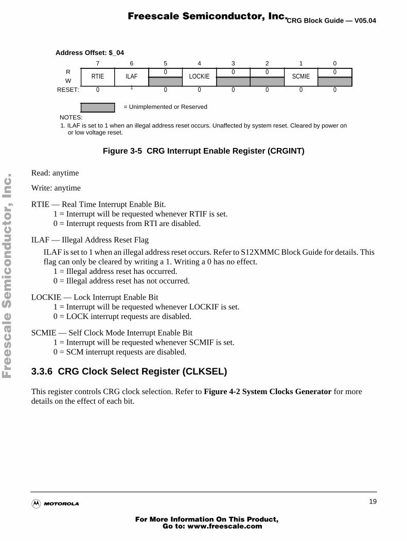
3.3.5 CRG Interrupt Enable Register (CRGINT)
This register enables CRG interrupt requests.
18
For More Information On This Product,
Go to: www.freescale.com
CRG Block Guide — V05.04
This
F
ree
sca
le S
em
ico
nd
uc
tor,
I
Freescale Semiconductor, Inc.n
c..
.
Figure 3-5 CRG Interrupt Enable Register (CRGINT)
Read: anytime
Write: anytime
RTIE — Real Time Interrupt Enable Bit.1 = Interrupt will be requested whenever RTIF is set.0 = Interrupt requests from RTI are disabled.
ILAF — Illegal Address Reset Flag
ILAF is set to 1 when an illegal address reset occurs. Refer to S12XMMC Block Guide for details.flag can only be cleared by writing a 1. Writing a 0 has no effect.
1 = Illegal address reset has occurred.0 = Illegal address reset has not occurred.
LOCKIE — Lock Interrupt Enable Bit1 = Interrupt will be requested whenever LOCKIF is set.0 = LOCK interrupt requests are disabled.
SCMIE — Self Clock Mode Interrupt Enable Bit1 = Interrupt will be requested whenever SCMIF is set.0 = SCM interrupt requests are disabled.
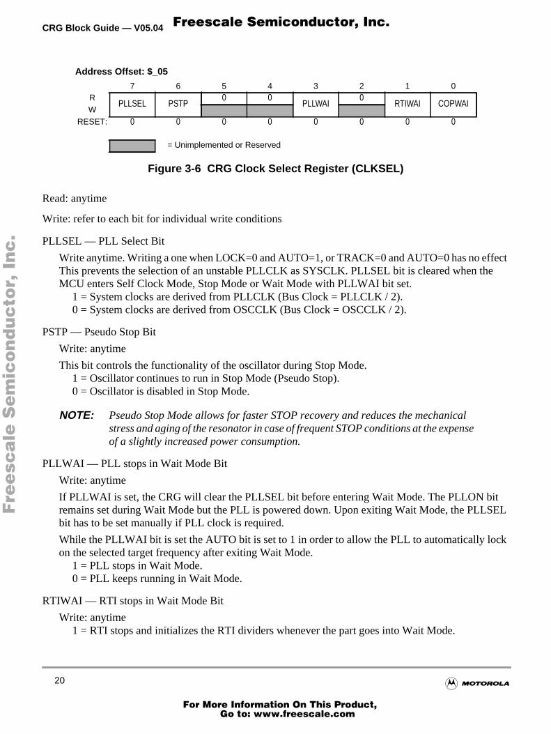
3.3.6 CRG Clock Select Register (CLKSEL)
This register controls CRG clock selection. Refer toFigure 4-2 System Clocks Generator for moredetails on the effect of each bit.
Address Offset: $_04
7 6 5 4 3 2 1 0R
RTIE ILAF0
LOCKIE0 0
SCMIE0
WRESET: 0 1
NOTES:1. ILAF is set to 1 when an illegal address reset occurs. Unaffected by system reset. Cleared by power on
or low voltage reset.
0 0 0 0 0 0
= Unimplemented or Reserved
19
For More Information On This Product,
Go to: www.freescale.com
CRG Block Guide — V05.04
ecthe
itEL
k
F
ree
sca
le S
em
ico
nd
uc
tor,
I
Freescale Semiconductor, Inc.n
c..
.
Figure 3-6 CRG Clock Select Register (CLKSEL)
Read: anytime
Write: refer to each bit for individual write conditions
PLLSEL — PLL Select Bit
Write anytime. Writing a one when LOCK=0 and AUTO=1, or TRACK=0 and AUTO=0 has no effThis prevents the selection of an unstable PLLCLK as SYSCLK. PLLSEL bit is cleared when tMCU enters Self Clock Mode, Stop Mode or Wait Mode with PLLWAI bit set.
1 = System clocks are derived from PLLCLK (Bus Clock = PLLCLK / 2).0 = System clocks are derived from OSCCLK (Bus Clock = OSCCLK / 2).
PSTP — Pseudo Stop Bit
Write: anytime
This bit controls the functionality of the oscillator during Stop Mode.1 = Oscillator continues to run in Stop Mode (Pseudo Stop).0 = Oscillator is disabled in Stop Mode.
NOTE: Pseudo Stop Mode allows for faster STOP recovery and reduces the mechanicalstress and aging of the resonator in case of frequent STOP conditions at the expenseof a slightly increased power consumption.
PLLWAI — PLL stops in Wait Mode Bit
Write: anytime
If PLLWAI is set, the CRG will clear the PLLSEL bit before entering Wait Mode. The PLLON bremains set during Wait Mode but the PLL is powered down. Upon exiting Wait Mode, the PLLSbit has to be set manually if PLL clock is required.
While the PLLWAI bit is set the AUTO bit is set to 1 in order to allow the PLL to automatically locon the selected target frequency after exiting Wait Mode.
1 = PLL stops in Wait Mode.0 = PLL keeps running in Wait Mode.
RTIWAI — RTI stops in Wait Mode Bit
Write: anytime1 = RTI stops and initializes the RTI dividers whenever the part goes into Wait Mode.
Address Offset: $_05
7 6 5 4 3 2 1 0R
PLLSEL PSTP0 0
PLLWAI0
RTIWAI COPWAIW
RESET: 0 0 0 0 0 0 0 0
= Unimplemented or Reserved
20
For More Information On This Product,
Go to: www.freescale.com

CRG Block Guide — V05.04
ce or
ds
F
ree
sca
le S
em
ico
nd
uc
tor,
I
Freescale Semiconductor, Inc.n
c..
.
0 = RTI keeps running in Wait Mode.
COPWAI — COP stops in Wait Mode Bit
Normal modes: Write once
Special modes: Write anytime1 = COP stops and initializes the COP counter whenever the part goes into Wait Mode.0 = COP keeps running in Wait Mode.
3.3.7 CRG PLL Control Register (PLLCTL)
This register controls the PLL functionality.
Figure 3-7 CRG PLL Control Register (PLLCTL)
Read: anytime
Write: refer to each bit for individual write conditions
CME — Clock Monitor Enable Bit
CME enables the clock monitor. Write anytime except when SCM = 1.1 = Clock monitor is enabled. Slow or stopped clocks will cause a clock monitor reset sequen
Self Clock Mode.0 = Clock monitor is disabled.
NOTE: Operating with CME=0 will not detect any loss of clock. In case of poor clockquality this could cause unpredictable operation of the MCU!
In Stop Mode (PSTP=0) the clock monitor is disabled independently of the CME bitsetting and any loss of external clock will not be detected.Also after wake-up from stop mode (PSTP=0) with fast wake-up enabled(FSTWKP=1) the clock monitor is disabled independently of the CME bit settingand any loss of external clock will not be detected.
PLLON — Phase Lock Loop On Bit
PLLON turns on the PLL circuitry. In Self Clock Mode, the PLL is turned on, but the PLLON bit reathe last latched value. Write anytime except when PLLSEL = 1.
1 = PLL is turned on. If AUTO bit is set, the PLL will lock automatically.0 = PLL is turned off.
Address Offset: $_06
7 6 5 4 3 2 1 0R
CME PLLON AUTO ACQ FSTWKP PRE PCE SCMEW
RESET: 1 1 1 1 0 0 0 1
= Unimplemented or Reserved
21
For More Information On This Product,
Go to: www.freescale.com

CRG Block Guide — V05.04
dehen
it.
led
tor all
F
ree
sca
le S
em
ico
nd
uc
tor,
I
Freescale Semiconductor, Inc.n
c..
.
AUTO — Automatic Bandwidth Control Bit
AUTO selects either the high bandwidth (acquisition) mode or the low bandwidth (tracking) modepending on how close to the desired frequency the VCO is running. Write anytime except wPLLWAI=1, because PLLWAI sets the AUTO bit to 1.
1 = Automatic Mode Control is enabled and ACQ bit has no effect.0 = Automatic Mode Control is disabled and the PLL is under software control, using ACQ b
ACQ — Acquisition Bit
Write anytime. If AUTO=1 this bit has no effect.1 = High bandwidth filter is selected.0 = Low bandwidth filter is selected.
FSTWKP— Fast Wake-up from Full Stop Bit
FSTWKP enables fast wake-up from full stop mode. Write anytime. If Self-Clock Mode is disab(SCME=0) this bit has no effect.
1 = Fast wake-up from full stop mode is enabled.When waking up from full stop mode the system will immediately resume operation inSelf-Clock Mode (see4.2.4 Clock Quality Checker). The SCMIF flag will not be set. Thesystem will remain in Self-Clock Mode with oscillator and clock monitor disabled untilFSTWKP bit is cleared. The clearing of FSTWKP will start the oscillator, the clock moniand the clock quality check. If the clock quality check is successful, the CRG will switchsystem clocks to OSCCLK. The SCMIF flag will be set. See application examples inFigure4-10 andFigure 4-11 .
0 = Fast wake-up from full stop mode is disabled.
PRE — RTI Enable during Pseudo Stop Bit
PRE enables the RTI during Pseudo Stop Mode. Write anytime.1 = RTI continues running during Pseudo Stop Mode.0 = RTI stops running during Pseudo Stop Mode.
NOTE: If the PRE bit is cleared the RTI dividers will go static while Pseudo Stop Mode isactive. The RTI dividers willnot initialize like in Wait Mode with RTIWAI bit set.
PCE — COP Enable during Pseudo Stop Bit
PCE enables the COP during Pseudo Stop Mode. Write anytime.1 = COP continues running during Pseudo Stop Mode0 = COP stops running during Pseudo Stop Mode
NOTE: If the PCE bit is cleared the COP dividers will go static while Pseudo Stop Mode isactive. The COP dividers willnot initialize like in Wait Mode with COPWAI bit set.
SCME — Self Clock Mode Enable Bit
Normal modes: Write once
Special modes: Write anytimeSCME can not be cleared while operating in Self Clock Mode (SCM=1).
0 = Detection of crystal clock failure causes clock monitor reset (see5.2.1 Clock Monitor Reset).
22
For More Information On This Product,
Go to: www.freescale.com

CRG Block Guide — V05.04
I is
F
ree
sca
le S
em
ico
nd
uc
tor,
I
Freescale Semiconductor, Inc.n
c..
.
1 = Detection of crystal clock failure forces the MCU in Self Clock Mode (see4.3.2 Self ClockMode).
3.3.8 CRG RTI Control Register (RTICTL)
This register selects the timeout period for the Real Time Interrupt.
Figure 3-8 CRG RTI Control Register (RTICTL)
Read: anytime
Write: anytime
NOTE: A write to this register initializes the RTI counter.
RTR[6:4] — Real Time Interrupt Prescale Rate Select Bits
These bits select the prescale rate for the RTI. SeeTable 3-2 andTable 3-3 .
RTR[3:0] — Real Time Interrupt Modulus Counter Select Bits
These bits select the modulus counter target value to provide additional granularity.Table 3-2 andTable3-3 show all possible divide values selectable by the RTICTL register. The source clock for the RTOSCCLK.
RTDEC— Decimal or Binary Divider Select Bit
RTDEC selects decimal or binary based prescaler values.1 = Decimal based divider value. SeeTable 3-30 = Binary based divider value. SeeTable 3-2
Address Offset: $_07
7 6 5 4 3 2 1 0R
RTDEC RTR6 RTR5 RTR4 RTR3 RTR2 RTR1 RTR0W
RESET: 0 0 0 0 0 0 0 0
= Unimplemented or Reserved
Table 3-2 RTI Frequency Divide Rates for RTDEC=0
RTR[3:0] RTR[6:4] =
000(OFF)
001(210)
010(211)
011(212)
100(213)
101(214)
110(215)
111(216)
0000 (÷1) OFF* 210 211 212 213 214 215 216
23
For More Information On This Product,
Go to: www.freescale.com
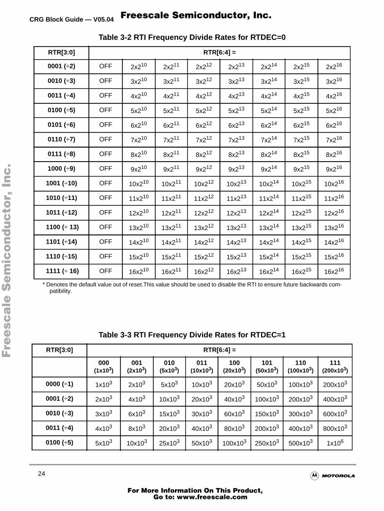
CRG Block Guide — V05.04
Fre
esc
ale
Se
mic
on
du
cto
r, I
Freescale Semiconductor, Inc.n
c..
.
0001 (÷2) OFF 2x210 2x211 2x212 2x213 2x214 2x215 2x216
0010 (÷3) OFF 3x210 3x211 3x212 3x213 3x214 3x215 3x216
0011 (÷4) OFF 4x210 4x211 4x212 4x213 4x214 4x215 4x216
0100 (÷5) OFF 5x210 5x211 5x212 5x213 5x214 5x215 5x216
0101 (÷6) OFF 6x210 6x211 6x212 6x213 6x214 6x215 6x216
0110 (÷7) OFF 7x210 7x211 7x212 7x213 7x214 7x215 7x216
0111 (÷8) OFF 8x210 8x211 8x212 8x213 8x214 8x215 8x216
1000 (÷9) OFF 9x210 9x211 9x212 9x213 9x214 9x215 9x216
1001 (÷10) OFF 10x210 10x211 10x212 10x213 10x214 10x215 10x216
1010 (÷11) OFF 11x210 11x211 11x212 11x213 11x214 11x215 11x216
1011 (÷12) OFF 12x210 12x211 12x212 12x213 12x214 12x215 12x216
1100 (÷ 13) OFF 13x210 13x211 13x212 13x213 13x214 13x215 13x216
1101 (÷14) OFF 14x210 14x211 14x212 14x213 14x214 14x215 14x216
1110 (÷15) OFF 15x210 15x211 15x212 15x213 15x214 15x215 15x216
1111 (÷ 16) OFF 16x210 16x211 16x212 16x213 16x214 16x215 16x216
* Denotes the default value out of reset.This value should be used to disable the RTI to ensure future backwards com-patibility.
Table 3-3 RTI Frequency Divide Rates for RTDEC=1
RTR[3:0] RTR[6:4] =
000(1x10³)
001(2x10³)
010(5x10³)
011(10x103)
100(20x103)
101(50x103)
110(100x103)
111(200x103)
0000 (÷1) 1x10³ 2x10³ 5x10³ 10x103 20x103 50x103 100x103 200x103
0001 (÷2) 2x10³ 4x10³ 10x103 20x103 40x103 100x103 200x103 400x103
0010 (÷3) 3x10³ 6x10³ 15x103 30x103 60x103 150x103 300x103 600x103
0011 (÷4) 4x10³ 8x10³ 20x103 40x103 80x103 200x103 400x103 800x103
0100 (÷5) 5x10³ 10x103 25x103 50x103 100x103 250x103 500x103 1x10⁶
Table 3-2 RTI Frequency Divide Rates for RTDEC=0
RTR[3:0] RTR[6:4] =
24
For More Information On This Product,
Go to: www.freescale.com

CRG Block Guide — V05.04
Fre
esc
ale
Se
mic
on
du
cto
r, I
Freescale Semiconductor, Inc.n
c..
.
3.3.9 CRG COP Control Register (COPCTL)
This register controls the COP (Computer Operating Properly) watchdog.
Figure 3-9 CRG COP Control Register (COPCTL)
Read: anytime
Write:
1) RSBCK: anytime in special modes; write to “1” but not to “0” in all other modes
2) WCOP, CR2, CR1, CR0:
• anytime in special modes
0101 (÷6) 6x10³ 12x103 30x103 60x103 120x103 300x103 600x103 1.2x10⁶
0110 (÷7) 7x10³ 14x103 35x103 70x103 140x103 350x103 700x103 1.4x10⁶
0111 (÷8) 8x10³ 16x103 40x103 80x103 160x103 400x103 800x103 1.6x10⁶
1000 (÷9) 9x10³ 18x103 45x103 90x103 180x103 450x103 900x103 1.8x10⁶
1001 (÷10) 10 x103 20x103 50x103 100x103 200x103 500x103 1x10⁶ 2x10⁶
1010 (÷11) 11 x103 22x103 55x103 110x103 220x103 550x103 1.1x10⁶ 2.2x10⁶
1011 (÷12) 12x103 24x103 60x103 120x103 240x103 600x103 1.2x10⁶ 2.4x10⁶
1100 (÷ 13) 13x103 26x103 65x103 130x103 260x103 650x103 1.3x10⁶ 2.6x10⁶
1101 (÷14) 14x103 28x103 70x103 140x103 280x103 700x103 1.4x10⁶ 2.8x10⁶
1110 (÷15) 15x103 30x103 75x103 150x103 300x103 750x103 1.5x10⁶ 3x10⁶
1111 (÷ 16) 16x103 32x103 80x103 160x103 320x103 800x103 1.6x10⁶ 3.2x10⁶
Address Offset: $_08
7 6 5 4 3 2 1 0R
WCOP RSBCK0 0 0
CR2 CR1 CR0W WRTMASK
RESET:1
NOTES:1. Refer to Device User Guide (Section: CRG) for reset values of WCOP, CR2, CR1 and CR0.
0 0 0 0
= Unimplemented or Reserved
Table 3-3 RTI Frequency Divide Rates for RTDEC=1
RTR[3:0] RTR[6:4] =
25
For More Information On This Product,
Go to: www.freescale.com

CRG Block Guide — V05.04
write thislogic
ts thedically
OPd):
F
ree
sca
le S
em
ico
nd
uc
tor,
I
Freescale Semiconductor, Inc.n
c..
.
• write once in all other modesWriting CR[2:0] to “000” has no effect, but counts for the “write once” condition.Writing WCOP to “0” has no effect, but counts for the “write once” condition.
The COP time-out period is restarted if one these two conditions is true:
1) Writing a non zero value to CR[2:0] (anytime in special modes, once in all other modes) withWRTMASK = 0.
or
2) Changing RSBCK bit from “0” to “1”.
WCOP — Window COP Mode Bit
When set, a write to the ARMCOP register must occur in the last 25% of the selected period. Aduring the first 75% of the selected period will reset the part. As long as all writes occur duringwindow, $55 can be written as often as desired. Once $AA is written after the $55, the time-outrestarts and the user must wait until the next window before writing to ARMCOP.Table 3-4 showsthe duration of this window for the seven available COP rates.
1 = Window COP operation0 = Normal COP operation
RSBCK — COP and RTI stop in Active BDM mode Bit1 = Stops the COP and RTI counters whenever the part is in Active BDM mode.0 = Allows the COP and RTI to keep running in Active BDM mode.
WRTMASK— Write mask for WCOP and CR[2:0] Bit
This write-only bit serves as a mask for the WCOP and CR[2:0] bits while writing the COPCTLregister. It is intended for BDM writing the RSBCK without touching the contents of WCOP andCR[2:0].
1 = Write of WCOP and CR[2:0] has no effect with this write of COPCTL.(Does not count for “write once”.)
0 = Write of WCOP and CR[2:0] has an effect with this write of COPCTL
CR[2:0] — COP Watchdog Timer Rate select
These bits select the COP time-out rate (seeTable 3-4). The COP time-out period is OSCCLK perioddivided by CR[2:0] value. Writing a nonzero value to CR[2:0] enables the COP counter and startime-out period. A COP counter time-out causes a system reset. This can be avoided by perio(before time-out) reinitializing the COP counter via the ARMCOP register.
While all of the following three conditions are true the CR[2:0], WCOP bits are ignored and the Coperates at highest time-out period (2 24 cycles) in normal COP mode (Window Cop mode disable1) BDM mode active
26
For More Information On This Product,
Go to: www.freescale.com

CRG Block Guide — V05.04
Fre
esc
ale
Se
mic
on
du
cto
r, I
Freescale Semiconductor, Inc.n
c..
.
2) RSBCK = 03) Operation in emulation or special modes
3.3.10 Reserved Register (FORBYP)
NOTE: This reserved register is designed for factory test purposes only, and is not intendedfor general user access. Writing to this register when in special modes can alter theCRG’s functionality.
Figure 3-10 Reserved Register (FORBYP)
Read: always read $00 except in special modes
Write: only in special modes
Table 3-4 COP Watchdog Rates 1
NOTES:1. OSCCLK cycles are referenced
from the previous COP time-outreset (writing $55/$AA to theARMCOP register)
CR2 CR1 CR0OSCCLKcycles totime-out
0 0 0COP
disabled
0 0 1 2 14
0 1 0 2 16
0 1 1 2 18
1 0 0 2 20
1 0 1 2 22
1 1 0 2 23
1 1 1 2 24
Address Offset: $_09
7 6 5 4 3 2 1 0R 0 0 0 0 0 0 0 0W
RESET: 0 0 0 0 0 0 0 0
= Unimplemented or Reserved
27
For More Information On This Product,
Go to: www.freescale.com

CRG Block Guide — V05.04
d youritesCOPis set,
F
ree
sca
le S
em
ico
nd
uc
tor,
I
Freescale Semiconductor, Inc.n
c..
.
3.3.11 Reserved Register (CTCTL)
NOTE: This reserved register is designed for factory test purposes only, and is not intendedfor general user access. Writing to this register when in special test modes can alterthe CRG’s functionality.
Figure 3-11 Reserved Register (CTCTL)
Read: always read $80 except in special modes
Write: only in special modes
3.3.12 CRG COP Timer Arm/Reset Register (ARMCOP)
This register is used to restart the COP time-out period.
Figure 3-12 ARMCOP Register Diagram
Read: always reads $00
Write: anytime
When the COP is disabled (CR[2:0] = “000”) writing to this register has no effect.
When the COP is enabled by setting CR[2:0] nonzero, the following applies:
Writing any value other than $55 or $AA causes a COP reset. To restart the COP time-out periomust write $55 followed by a write of $AA. Other instructions may be executed between these wbut the sequence ($55, $AA) must be completed prior to COP end of time-out period to avoid areset. Sequences of $55 writes or sequences of $AA writes are allowed. When the WCOP bit
Address Offset: $_0A
7 6 5 4 3 2 1 0R 1 0 0 0 0 0 0 0W
RESET: 0 0 0 0 0 0 0 0
= Unimplemented or Reserved
Address Offset: $_0B
7 6 5 4 3 2 1 0R 0 0 0 0 0 0 0 0W Bit 7 Bit 6 Bit 5 Bit 4 Bit 3 Bit 2 Bit 1 Bit 0
RESET: 0 0 0 0 0 0 0 0
= Unimplemented or Reserved
28
For More Information On This Product,
Go to: www.freescale.com

CRG Block Guide — V05.04
ue in
F
ree
sca
le S
em
ico
nd
uc
tor,
I
Freescale Semiconductor, Inc.n
c..
.
$55 and $AA writes must be done in the last 25% of the selected time-out period; writing any valthe first 75% of the selected period will cause a COP reset.
29
For More Information On This Product,
Go to: www.freescale.com

CRG Block Guide — V05.04
Fre
esc
ale
Se
mic
on
du
cto
r, I
Freescale Semiconductor, Inc.n
c..
.
30
For More Information On This Product,
Go to: www.freescale.com
CRG Block Guide — V05.04
asedffers...
ing oneen
f
F
ree
sca
le S
em
ico
nd
uc
tor,
I
Freescale Semiconductor, Inc.n
c..
.
Section 4 Functional Description
4.1 General
This section gives detailed informations on the internal operation of the design.
4.2 Functional Blocks
4.2.1 Phase Locked Loop (PLL)
The PLL is used to run the MCU from a different time base than the incoming OSCCLK. For increflexibility, OSCCLK can be divided in a range of 1 to 16 to generate the reference frequency. This oa finer multiplication granularity. The PLL can multiply this reference clock by a multiple of 2, 4, 6,126,128 based on the SYNR register.
CAUTION: Although it is possible to set the two dividers to command a very high clockfrequency, do not exceed the specified bus frequency limit for the MCU.If (PLLSEL=1), Bus Clock = PLLCLK / 2
The PLL is a frequency generator that operates in either acquisition mode or tracking mode, dependthe difference between the output frequency and the target frequency. The PLL can change betwacquisition and tracking modes either automatically or manually.
The VCO has a minimum operating frequency, which corresponds to the self clock mode frequencySCM.
Figure 4-1 PLL Functional Diagram
PLLCLK 2 OSCCLKSYNR 1+[ ]
REFDV 1+[ ]------------------------------------××=
REDUCEDCONSUMPTION
OSCILLATOR
EXTAL
XTAL
OSCCLK
PLLCLK
REFERENCEPROGRAMMABLE
DIVIDER PDETPHASE
DETECTOR
REFDV <3:0>
LOOPPROGRAMMABLE
DIVIDER
SYN <5:0>
CPUMP VCO
LOCK
LOOPFILTER
XFCPIN
UP
DOWN
LOCKDETECTOR
REFERENCE
FEEDBACK
VDDPLL
VDDPLL/VSSPLL
CRYSTALMONITOR
VDDPLL/VSSPLL
VDD/VSS
supplied by:
31
For More Information On This Product,
Go to: www.freescale.com
CRG Block Guide — V05.04
nd is, in
ulsesters thef the in thespeed
k.he
es:
usedar offFLG
r iskingster.
ly.
enn therupt. Ifally)e as coreke
F
ree
sca
le S
em
ico
nd
uc
tor,
I
Freescale Semiconductor, Inc.n
c..
.
4.2.1.1 PLL Operation
The oscillator output clock signal (OSCCLK) is fed through the reference programmable divider adivided in a range of 1 to 16 (REFDV+1) to output the REFERENCE clock. The VCO output clock(PLLCLK) is fed back through the programmable loop divider and is divided in a range of 2 to 128increments of [2 x (SYNR +1)] to output the FEEDBACK clock. SeeFigure 4-1.
The phase detector then compares the FEEDBACK clock, with the REFERENCE clock. Correction pare generated based on the phase difference between the two signals. The loop filter then slightly alDC voltage on the external filter capacitor connected to XFC pin, based on the width and direction ocorrection pulse. The filter can make fast or slow corrections depending on its mode, as describednext subsection. The values of the external filter network and the reference frequency determine theof the corrections and the stability of the PLL.
4.2.1.2 Acquisition and Tracking Modes
The lock detector compares the frequencies of the FEEDBACK clock, and the REFERENCE clocTherefore, the speed of the lock detector is directly proportional to the final reference frequency. Tcircuit determines the mode of the PLL and the lock condition based on this comparison.
The PLL filter can be manually or automatically configured into one of two possible operating mod
• Acquisition mode
In acquisition mode, the filter can make large frequency corrections to the VCO. This mode isat PLL start-up or when the PLL has suffered a severe noise hit and the VCO frequency is fthe desired frequency. When in acquisition mode, the TRACK status bit is cleared in the CRGregister.
• Tracking mode
In tracking mode, the filter makes only small corrections to the frequency of the VCO. PLL jittemuch lower in tracking mode, but the response to noise is also slower. The PLL enters tracmode when the VCO frequency is nearly correct and the TRACK bit is set in the CRGFLG regi
The PLL can change the bandwidth or operational mode of the loop filter manually or automatical
In automatic bandwidth control mode (AUTO = 1), the lock detector automatically switches betweacquisition and tracking modes. Automatic bandwidth control mode also is used to determine whePLL clock (PLLCLK) is safe to use as the source for the system and core clocks. If PLL LOCK interrequests are enabled, the software can wait for an interrupt request and then check the LOCK bitinterrupt requests are disabled, software can poll the LOCK bit continuously (during PLL start-up, usuor at periodic intervals. In either case, only when the LOCK bit is set, is the PLLCLK clock safe to usthe source for the system and core clocks. If the PLL is selected as the source for the system andclocks and the LOCK bit is clear, the PLL has suffered a severe noise hit and the software must taappropriate action, depending on the application.
The following conditions apply when the PLL is in automatic bandwidth control mode (AUTO=1):
• The TRACK bit is a read-only indicator of the mode of the filter.
32
For More Information On This Product,
Go to: www.freescale.com

CRG Block Guide — V05.04
ling
notelown
F
ree
sca
le S
em
ico
nd
uc
tor,
I
Freescale Semiconductor, Inc.n
c..
.
• The TRACK bit is set when the VCO frequency is within a certain tolerance,∆trk, and is clear whenthe VCO frequency is out of a certain tolerance,∆unt.
• The LOCK bit is a read-only indicator of the locked state of the PLL.
• The LOCK bit is set when the VCO frequency is within a certain tolerance,∆Lock, and is clearedwhen the VCO frequency is out of a certain tolerance,∆unl.
• Interrupt requests can occur if enabled (LOCKIE = 1) when the lock condition changes, toggthe LOCK bit.
The PLL can also operate in manual mode (AUTO = 0). Manual mode is used by systems that dorequire an indicator of the lock condition for proper operation. Such systems typically operate well bthe maximum system frequency (fsys) and require fast start-up. The following conditions apply when imanual mode:
• ACQ is a writable control bit that controls the mode of the filter. Before turning on the PLL inmanual mode, the ACQ bit should be asserted to configure the filter in acquisition mode.
• After turning on the PLL by setting the PLLON bit software must wait a given time (tacq) beforeentering tracking mode (ACQ = 0).
• After entering tracking mode software must wait a given time (tal) before selecting the PLLCLK asthe source for system and core clocks (PLLSEL = 1).
33
For More Information On This Product,
Go to: www.freescale.com
CRG Block Guide — V05.04
the
k. The
. Thee
utrnedum
F
ree
sca
le S
em
ico
nd
uc
tor,
I
Freescale Semiconductor, Inc.n
c..
.
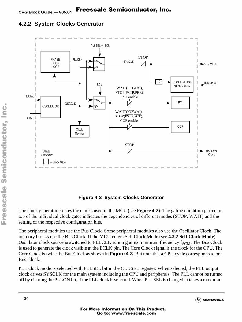
4.2.2 System Clocks Generator
Figure 4-2 System Clocks Generator
The clock generator creates the clocks used in the MCU (seeFigure 4-2). The gating condition placed ontop of the individual clock gates indicates the dependencies of different modes (STOP, WAIT) andsetting of the respective configuration bits.
The peripheral modules use the Bus Clock. Some peripheral modules also use the Oscillator Clocmemory blocks use the Bus Clock. If the MCU enters Self Clock Mode (see4.3.2 Self Clock Mode)Oscillator clock source is switched to PLLCLK running at its minimum frequency fSCM. The Bus Clockis used to generate the clock visible at the ECLK pin. The Core Clock signal is the clock for the CPUCore Clock is twice the Bus Clock as shown inFigure 4-3 . But note that a CPU cycle corresponds to onBus Clock.
PLL clock mode is selected with PLLSEL bit in the CLKSEL register. When selected, the PLL outpclock drives SYSCLK for the main system including the CPU and peripherals. The PLL cannot be tuoff by clearing the PLLON bit, if the PLL clock is selected. When PLLSEL is changed, it takes a maxim
OSCILLATOR
PHASELOCKLOOP
EXTAL
XTAL
SYSCLK
RTIOSCCLK
PLLCLK
CLOCK PHASEGENERATOR
Bus Clock
ClockMonitor
1
0
PLLSEL or SCM
÷2
Core Clock
COP
Oscillator
= Clock Gate
GatingCondition
WAIT(RTIWAI),STOP(PSTP,PRE),
RTI enable
WAIT(COPWAI),STOP(PSTP,PCE),
COP enable
STOP
1
0
SCM
Clock
STOP
34
For More Information On This Product,
Go to: www.freescale.com
CRG Block Guide — V05.04
and
k reset
ectedME
er
F
ree
sca
le S
em
ico
nd
uc
tor,
I
Freescale Semiconductor, Inc.n
c..
.
of 4 OSCCLK plus 4 PLLCLK cycles to make the transition. During the transition, all clocks freezeCPU activity ceases.
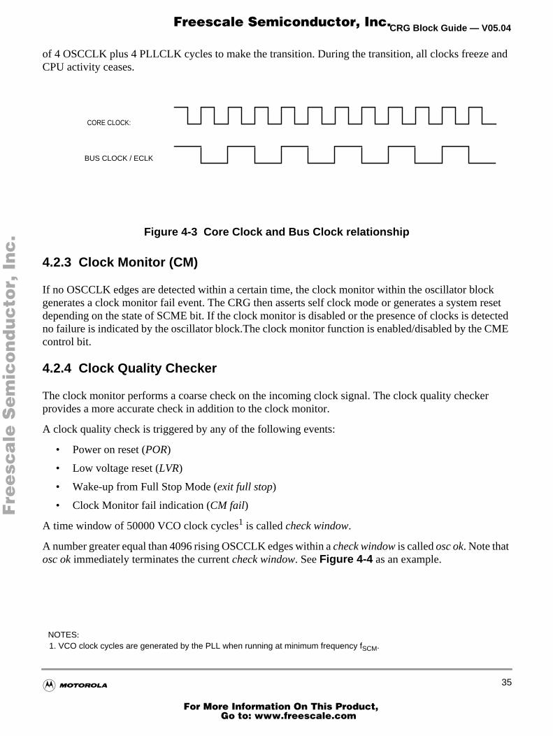
Figure 4-3 Core Clock and Bus Clock relationship
4.2.3 Clock Monitor (CM)
If no OSCCLK edges are detected within a certain time, the clock monitor within the oscillator blocgenerates a clock monitor fail event. The CRG then asserts self clock mode or generates a systemdepending on the state of SCME bit. If the clock monitor is disabled or the presence of clocks is detno failure is indicated by the oscillator block.The clock monitor function is enabled/disabled by the Ccontrol bit.
4.2.4 Clock Quality Checker
The clock monitor performs a coarse check on the incoming clock signal. The clock quality checkprovides a more accurate check in addition to the clock monitor.
A clock quality check is triggered by any of the following events:
• Power on reset (POR)
• Low voltage reset (LVR)
• Wake-up from Full Stop Mode (exit full stop)
• Clock Monitor fail indication (CM fail)
A time window of 50000 VCO clock cycles1 is calledcheck window.
A number greater equal than 4096 rising OSCCLK edges within acheck windowis calledosc ok. Note thatosc ok immediately terminates the currentcheck window. SeeFigure 4-4 as an example.
NOTES:1. VCO clock cycles are generated by the PLL when running at minimum frequency fSCM.
CORE CLOCK:
BUS CLOCK / ECLK
35
For More Information On This Product,
Go to: www.freescale.com

CRG Block Guide — V05.04
Fre
esc
ale
Se
mic
on
du
cto
r, I
Freescale Semiconductor, Inc.n
c..
.
Figure 4-4 Check Window Example
The Sequence for clock quality check is shown inFigure 4-5 .
1 2 49999 50000VCOclock
check window
1 2 3 4 5
4095
4096
3
OSCCLK
osc ok
36
For More Information On This Product,
Go to: www.freescale.com

CRG Block Guide — V05.04
Fre
esc
ale
Se
mic
on
du
cto
r, I
Freescale Semiconductor, Inc.n
c..
.
Figure 4-5 Sequence for Clock Quality Check
NOTE: Remember that in parallel to additional actions caused by Self Clock Mode orClock Monitor Reset1 handling the clock quality checkercontinues to check theOSCCLK signal.
NOTE: The Clock Quality Checker enables the PLL and the voltage regulator (VREG)anytime a clock check has to be performed. An ongoing clock quality check couldalso cause a running PLL (fSCM) and an active VREG during Pseudo Stop Mode orWait Mode
NOTES:1. A Clock Monitor Reset will always set the SCME bit to logical’1’
check window
osc ok?
SCMactive?
Switch to OSCCLK
Exit SCM
Clock OK
num=50
num > 0?
num=num-1
yes
no
yes
SCME=1?
no
Enter SCM
SCMactive?
yes
Clock Monitor Reset
no
yes
no
num=0
yesno
PORexit full stop
CM fail
LVRSCME=1 &
?FSTWKP=1
yes
no?
FSTWKP=0
no
num=0 Enter SCM
yes
37
For More Information On This Product,
Go to: www.freescale.com

CRG Block Guide — V05.04
ware
out
terogram is
tes toeriod.
F
ree
sca
le S
em
ico
nd
uc
tor,
I
Freescale Semiconductor, Inc.n
c..
.
4.2.5 Computer Operating Properly Watchdog (COP)
Figure 4-6 Clock Chain for COP
The COP (free running watchdog timer) enables the user to check that a program is running andsequencing properly. The COP is disabled out of reset. When the COP is being used, software isresponsible for keeping the COP from timing out. If the COP times out it is an indication that the softis no longer being executed in the intended sequence; thus a system reset is initiated (see5.2.2 ComputerOperating Properly Watchdog (COP) Reset). The COP runs with a gated OSCCLK (seeFigure 4-6Clock Chain for COP). Three control bits in the COPCTL register allow selection of seven COP time-periods.
When COP is enabled, the program must write $55 and $AA (in this order) to the ARMCOP regisduring the selected time-out period. Once this is done, the COP time-out period is restarted. If the prfails to do this and the COP times out, the part will reset. Also, if any value other than $55 or $AAwritten, the part is immediately reset.
Windowed COP operation is enabled by setting WCOP in the COPCTL register. In this mode, writhe ARMCOP register to clear the COP timer must occur in the last 25% of the selected time-out pA premature write will immediately reset the part.
If PCE bit is set, the COP will continue to run in Pseudo Stop Mode.
OSCCLK
CR[2:0]
COP TIMEOUT
0:0:00:0:1
0:1:0
0:1:1
1:0:0
1:0:1
1:1:0
1:1:1
÷ 4
÷ 4
÷ 2
÷ 4
÷ 2
÷ 16384
÷ 4
CR[2:0]
= Clock Gate
WAIT(COPWAI),STOP(PSTP,PCE),
COP enable
gating condition
38
For More Information On This Product,
Go to: www.freescale.com

CRG Block Guide — V05.04
gated
F
ree
sca
le S
em
ico
nd
uc
tor,
I
Freescale Semiconductor, Inc.n
c..
.
4.2.6 Real Time Interrupt (RTI)
The RTI can be used to generate a hardware interrupt at a fixed periodic rate. If enabled (by settinRTIE=1), this interrupt will occur at the rate selected by the RTICTL register. The RTI runs with a gOSCCLK (seeFigure 4-7 Clock Chain for RTI ). At the end of the RTI time-out period the RTIF flag isset to one and a new RTI time-out period starts immediately.
A write to the RTICTL register restarts the RTI time-out period.
If the PRE bit is set, the RTI will continue to run in Pseudo Stop Mode.
.
Figure 4-7 Clock Chain for RTI
4.3 Operation Modes
4.3.1 Normal Mode
The CRG block behaves as described within this specification in all normal modes.
OSCCLK
RTR[6:4]0:0:0
0:0:1
0:1:0
0:1:1
1:0:0
1:0:1
1:1:0
1:1:1
÷ 2
÷ 2
÷ 2
÷ 2
÷ 2
÷ 2
COUNTER (RTR[3:0])4-BIT MODULUS
÷ 1024
RTI TIMEOUT= Clock Gate
WAIT(RTIWAI),STOP(PSTP,PRE),
RTI enable
gating condition
39
For More Information On This Product,
Go to: www.freescale.com

CRG Block Guide — V05.04
e the
Thisck
ill
ing of
Waitait
RG
F
ree
sca
le S
em
ico
nd
uc
tor,
I
Freescale Semiconductor, Inc.n
c..
.
4.3.2 Self Clock Mode
The VCO has a minimum operating frequency, fSCM. If the external clock frequency is not available duto a failure or due to long crystal start-up time, the Bus Clock and the Core Clock are derived fromVCO running at minimum operating frequency; this mode of operation is called Self Clock Mode. requires CME=1 and SCME=1. If the MCU was clocked by the PLL clock prior to entering Self CloMode, the PLLSEL bit will be cleared. If the external clock signal has stabilized again, the CRG wautomatically select OSCCLK to be the system clock and return to normal mode. See4.2.4 Clock QualityChecker for more information on entering and leaving Self Clock Mode.
NOTE: In order to detect a potential clock loss the CME bit should be always enabled(CME=1)!
If CME bit is disabled and the MCU is configured to run on PLL clock (PLLCLK),a loss of external clock (OSCCLK) will not be detected and will cause the systemclock to drift towards the VCO’s minimum frequency fSCM. As soon as the externalclock is available again the system clock ramps up to its PLL target frequency. Ifthe MCU is running on external clock any loss of clock will cause the system to gostatic.
4.4 Low Power Options
This section summarizes the low power options available in the CRG.
4.4.1 Run Mode
The RTI can be stopped by setting the associated rate select bits to zero.
The COP can be stopped by setting the associated rate select bits to zero.
4.4.2 Wait Mode
The WAI instruction puts the MCU in a low power consumption stand-by mode depending on settthe individual bits in the CLKSEL register. All individual Wait Mode configuration bits can besuperposed. This provides enhanced granularity in reducing the level of power consumption duringMode.Table 4-1 lists the individual configuration bits and the parts of the MCU that are affected in WMode.
After executing the WAI instruction the core requests the CRG to switch MCU into Wait Mode. The Cthen checks whether the PLLWAI bit is asserted (seeFigure 4-8 Wait Mode Entry/Exit Sequence).
Table 4-1 MCU configuration during Wait Mode
PLLWAI RTIWAI COPWAI
PLL stopped - -
RTI - stopped -
COP - - stopped
40
For More Information On This Product,
Go to: www.freescale.com
CRG Block Guide — V05.04
ng theitched
F
ree
sca
le S
em
ico
nd
uc
tor,
I
Freescale Semiconductor, Inc.n
c..
.
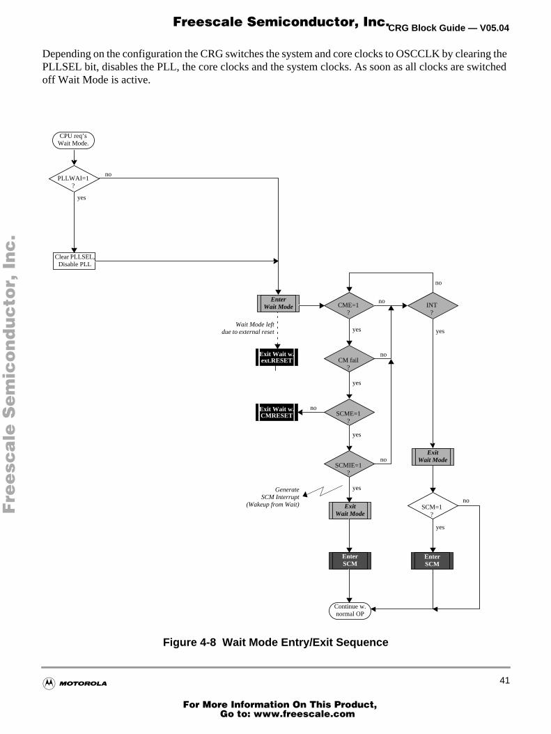
Depending on the configuration the CRG switches the system and core clocks to OSCCLK by cleariPLLSEL bit, disables the PLL, the core clocks and the system clocks. As soon as all clocks are swoff Wait Mode is active.
Figure 4-8 Wait Mode Entry/Exit Sequence
EnterWait Mode
PLLWAI=1?
Exit Wait w.CMRESET
Exit Wait w.ext.RESET
ExitWait Mode
EnterSCM
ExitWait Mode
CPU req’sWait Mode.
Clear PLLSEL,Disable PLL
CME=1?
INT?
CM fail?
SCME=1?
SCMIE=1?
Continue w.normal OP
no
no
no
no
no
yes
yes
yes
yes
yes
no
yes
Wait Mode leftdue to external reset
GenerateSCM Interrupt
(Wakeup from Wait) SCM=1?
EnterSCM
no
yes
41
For More Information On This Product,
Go to: www.freescale.com

CRG Block Guide — V05.04
storesr
t Mode
G
e. If the the
=0,-up
ith and bit
til
F
ree
sca
le S
em
ico
nd
uc
tor,
I
Freescale Semiconductor, Inc.n
c..
.
There are four different scenarios for the CRG to restart the MCU from Wait Mode:
• External Reset
• Clock Monitor Reset
• COP Reset
• Wake-up Interrupt
If the MCU gets an external reset or COP reset during Wait Mode active, the CRG asynchronously reall configuration bits in the register space to its default settings and starts the reset generator. Aftecompleting the reset sequence processing begins by fetching the normal or COP reset vector. Waiis left and the MCU is in Run Mode again.
If the clock monitor is enabled (CME=1) the MCU is able to leave Wait-Mode when loss ofoscillator/external clock is detected by a clock monitor fail. If the SCME bit is not asserted the CRgenerates a clock monitor fail reset (CMRESET). The CRG’s behavior for CMRESET is the samecompared to external reset, but another reset vector is fetched after completion of the reset sequencSCME bit is asserted the CRG generates a SCM interrupt if enabled (SCMIE=1). After generatinginterrupt the CRG enters Self-Clock Mode and starts the clock quality checker (see4.2.4 Clock QualityChecker). Then the MCU continues with normal operation.If the SCM interrupt is blocked by SCMIEthe SCMIF flag will be asserted and clock quality checks will be performed but the MCU will not wakefrom Wait-Mode.
If any other interrupt source (e.g. RTI) triggers exit from Wait Mode the MCU immediately continues wnormal operation. If the PLL has been powered-down during Wait-Mode the PLLSEL bit is clearedthe MCU runs on OSCCLK after leaving Wait-Mode. The software must manually set the PLLSELagain, in order to switch system and core clocks to the PLLCLK.
If Wait Mode is entered from Self-Clock Mode the CRG will continue to check the clock quality unclock check is successful. The PLL and voltage regulator (VREG) will remain enabled.
Table 4-2 summarizes the outcome of a clock loss while in Wait Mode.
Table 4-2 Outcome of Clock Loss in Wait Mode
CME SCME SCMIE CRG Actions
0 X XClock failure --> No action, clock loss not detected.
1 0 XClock failure --> CRG performs Clock Monitor Reset immediately
42
For More Information On This Product,
Go to: www.freescale.com

CRG Block Guide — V05.04
Fre
esc
ale
Se
mic
on
du
cto
r, I
Freescale Semiconductor, Inc.n
c..
.
1 1 0
Clock failure -->
Scenario 1: OSCCLK recovers prior to exiting Wait Mode. – MCU remains in Wait Mode, – VREG enabled, – PLL enabled, – SCM activated, – Start Clock Quality Check, – Set SCMIF interrupt flag.
Some time later OSCCLK recovers.
– CM no longer indicates a failure, – 4096 OSCCLK cycles later Clock Quality Check indicates clock o.k., – SCM deactivated, – PLL disabled depending on PLLWAI, – VREG remains enabled (never gets disabled in Wait Mode). – MCU remains in Wait Mode.
Some time later either a wakeup interrupt occurs (no SCM interrupt) – Exit Wait Mode using OSCCLK as system clock (SYSCLK), – Continue normal operation.
or an External Reset is applied. – Exit Wait Mode using OSCCLK as system clock, – Start reset sequence.
Scenario 2: OSCCLK does not recover prior to exiting Wait Mode. – MCU remains in Wait Mode, – VREG enabled, – PLL enabled, – SCM activated, – Start Clock Quality Check, – Set SCMIF interrupt flag, – Keep performing Clock Quality Checks (could continue infinitely) while in Wait Mode.
Some time later either a wakeup interrupt occurs (no SCM interrupt) – Exit Wait Mode in SCM using PLL clock (fSCM) as system clock, – Continue to perform additional Clock Quality Checks until OSCCLK is o.k. again.
or an External RESET is applied. – Exit Wait Mode in SCM using PLL clock (fSCM) as system clock, – Start reset sequence, – Continue to perform additional Clock Quality Checks until OSCCLK is o.k.again.
Table 4-2 Outcome of Clock Loss in Wait Mode
CME SCME SCMIE CRG Actions
43
For More Information On This Product,
Go to: www.freescale.com

CRG Block Guide — V05.04
heen bute. In
(e.g.ence
ocksandactive.
clockd. If
F
ree
sca
le S
em
ico
nd
uc
tor,
I
Freescale Semiconductor, Inc.n
c..
.
4.4.3 System Stop Mode
All clocks are stopped in STOP mode, dependent of the setting of the PCE, PRE and PSTP bit. Toscillator is disabled in STOP mode unless the PSTP bit is set. All counters and dividers remain frozdo not initialize. If the PRE or PCE bits are set, the RTI or COP continues to run in Pseudo Stop Modaddition to disabling system and core clocks the CRG requests other functional units of the MCU voltage-regulator) to enter their individual powersaving modes (if available). This is the main differbetween Pseudo Stop Mode and Wait Mode.
If the PLLSEL bit is still set when entering Stop Mode, the CRG will switch the system and core clto OSCCLK by clearing the PLLSEL bit. Then the CRG disables the PLL, disables the core clock finally disables the remaining system clocks. As soon as all clocks are switched off Stop Mode is
If Pseudo Stop Mode (PSTP=1) is entered from Self-Clock Mode the CRG will continue to check thequality until clock check is successful. The PLL and the voltage regulator (VREG) will remain enableFull Stop Mode (PSTP=0) is entered from Self-Clock Mode an ongoing clock quality check will bestopped. A complete timeout window check will be started when Stop Mode is left again.
Wake-up from Stop Mode also depends on the setting of the PSTP bit.
1 1 1
Clock failure --> – VREG enabled, – PLL enabled, – SCM activated, – Start Clock Quality Check, – SCMIF set.
SCMIF generates Self Clock Mode wakeup interrupt.
– Exit Wait Mode in SCM using PLL clock (fSCM) as system clock, – Continue to perform a additional Clock Quality Checks until OSCCLK is o.k. again.
Table 4-2 Outcome of Clock Loss in Wait Mode
CME SCME SCMIE CRG Actions
44
For More Information On This Product,
Go to: www.freescale.com

CRG Block Guide — V05.04
ferent
F
ree
sca
le S
em
ico
nd
uc
tor,
I
Freescale Semiconductor, Inc.n
c..
.
Figure 4-9 Stop Mode Entry/Exit Sequence
4.4.3.1 Wake-up from Pseudo Stop Mode (PSTP=1)
Wake-up from Pseudo Stop Mode is the same as wake-up from Wait Mode. There are also four difscenarios for the CRG to restart the MCU from Pseudo Stop Mode:
Exit Stop w.CMRESET
ExitStop Mode
EnterSCM
ExitStop Mode
Core req’sStop Mode.
Clear PLLSEL,Disable PLL
CME=1?
INT?
CM fail?
SCME=1?
SCMIE=1?
Continue w.normal OP
no
no
no
no
yes
yes
yes
yes
yes
GenerateSCM Interrupt
(Wakeup from Stop)
EnterStop Mode
Exit Stop w.ext.RESET
Stop Mode leftdue to external reset
ClockOK?
SCME=1?
EnterSCM
yes
no
yes
Exit Stop w.CMRESET
no
nono
PSTP=1?
INT?
yesno
yes
ExitStop Mode
ExitStop Mode
SCM=1?
EnterSCM
no
yes
yes
no
SCME=1 &FSTWKP=1
?
ExitStop Mode
Enter SCMSCMIF not
set!
45
For More Information On This Product,
Go to: www.freescale.com

CRG Block Guide — V05.04
nouslyr. Afterdo Stop
fG
e. If the the
=0,
et set
F
ree
sca
le S
em
ico
nd
uc
tor,
I
Freescale Semiconductor, Inc.n
c..
.
• External Reset
• Clock Monitor Reset
• COP Reset
• Wake-up Interrupt
If the MCU gets an external reset or COP reset during Pseudo Stop Mode active, the CRG asynchrorestores all configuration bits in the register space to its default settings and starts the reset generatocompleting the reset sequence processing begins by fetching the normal or COP reset vector. PseuMode is left and the MCU is in Run Mode again.
If the clock monitor is enabled (CME=1) the MCU is able to leave Pseudo Stop Mode when loss ooscillator/external clock is detected by a clock monitor fail. If the SCME bit is not asserted the CRgenerates a clock monitor fail reset (CMRESET). The CRG’s behavior for CMRESET is the samecompared to external reset, but another reset vector is fetched after completion of the reset sequencSCME bit is asserted the CRG generates a SCM interrupt if enabled (SCMIE=1). After generatinginterrupt the CRG enters Self-Clock Mode and starts the clock quality checker (see4.2.4 Clock QualityChecker). Then the MCU continues with normal operation. If the SCM interrupt is blocked by SCMIEthe SCMIF flag will be asserted but the CRG will not wake-up from Pseudo Stop Mode.
If any other interrupt source (e.g. RTI) triggers exit from Pseudo Stop Mode the MCU immediatelycontinues with normal operation. Because the PLL has been powered-down during Stop Mode thPLLSEL bit is cleared and the MCU runs on OSCCLK after leaving Stop Mode. The software musthe PLLSEL bit again, in order to switch system and core clocks to the PLLCLK.
Table 4-3 summarizes the outcome of a clock loss while in Pseudo Stop Mode.
Table 4-3 Outcome of Clock Loss in Pseudo Stop Mode
CME SCME SCMIE CRG Actions
0 X XClock failure --> No action, clock loss not detected.
1 0 XClock failure --> CRG performs Clock Monitor Reset immediately
46
For More Information On This Product,
Go to: www.freescale.com
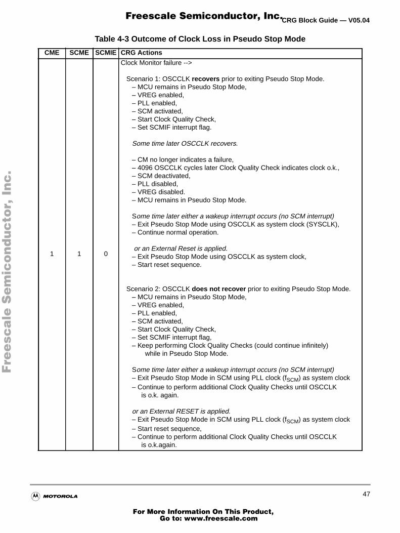
CRG Block Guide — V05.04
Fre
esc
ale
Se
mic
on
du
cto
r, I
Freescale Semiconductor, Inc.n
c..
.
1 1 0
Clock Monitor failure -->
Scenario 1: OSCCLK recovers prior to exiting Pseudo Stop Mode. – MCU remains in Pseudo Stop Mode, – VREG enabled, – PLL enabled, – SCM activated, – Start Clock Quality Check, – Set SCMIF interrupt flag.
Some time later OSCCLK recovers.
– CM no longer indicates a failure, – 4096 OSCCLK cycles later Clock Quality Check indicates clock o.k., – SCM deactivated, – PLL disabled, – VREG disabled. – MCU remains in Pseudo Stop Mode.
Some time later either a wakeup interrupt occurs (no SCM interrupt) – Exit Pseudo Stop Mode using OSCCLK as system clock (SYSCLK), – Continue normal operation.
or an External Reset is applied. – Exit Pseudo Stop Mode using OSCCLK as system clock, – Start reset sequence.
Scenario 2: OSCCLK does not recover prior to exiting Pseudo Stop Mode. – MCU remains in Pseudo Stop Mode, – VREG enabled, – PLL enabled, – SCM activated, – Start Clock Quality Check, – Set SCMIF interrupt flag, – Keep performing Clock Quality Checks (could continue infinitely) while in Pseudo Stop Mode.
Some time later either a wakeup interrupt occurs (no SCM interrupt) – Exit Pseudo Stop Mode in SCM using PLL clock (fSCM) as system clock – Continue to perform additional Clock Quality Checks until OSCCLK is o.k. again.
or an External RESET is applied. – Exit Pseudo Stop Mode in SCM using PLL clock (fSCM) as system clock – Start reset sequence, – Continue to perform additional Clock Quality Checks until OSCCLK is o.k.again.
Table 4-3 Outcome of Clock Loss in Pseudo Stop Mode
CME SCME SCMIE CRG Actions
47
For More Information On This Product,
Go to: www.freescale.com
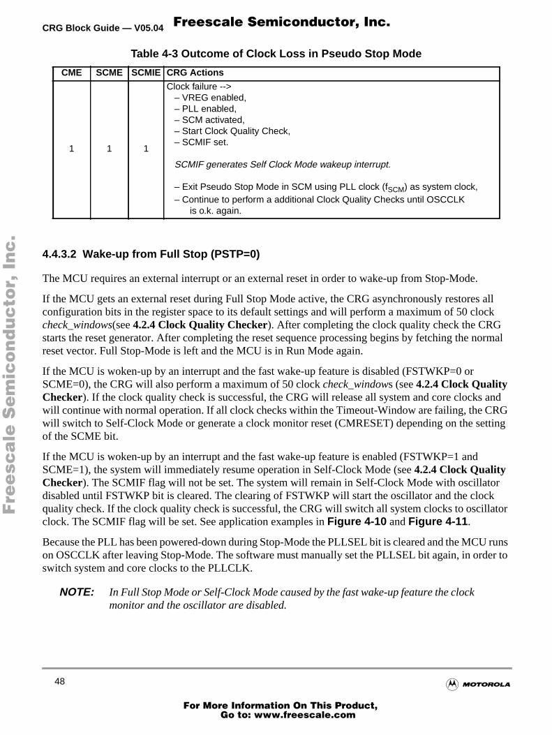
CRG Block Guide — V05.04
allck
normal
andGtting
rk
ator
runser to
F
ree
sca
le S
em
ico
nd
uc
tor,
I
Freescale Semiconductor, Inc.n
c..
.
4.4.3.2 Wake-up from Full Stop (PSTP=0)
The MCU requires an external interrupt or an external reset in order to wake-up from Stop-Mode.
If the MCU gets an external reset during Full Stop Mode active, the CRG asynchronously restoresconfiguration bits in the register space to its default settings and will perform a maximum of 50 clocheck_windows(see4.2.4 Clock Quality Checker). After completing the clock quality check the CRGstarts the reset generator. After completing the reset sequence processing begins by fetching thereset vector. Full Stop-Mode is left and the MCU is in Run Mode again.
If the MCU is woken-up by an interrupt and the fast wake-up feature is disabled (FSTWKP=0 orSCME=0), the CRG will also perform a maximum of 50 clockcheck_windows (see4.2.4 Clock QualityChecker). If the clock quality check is successful, the CRG will release all system and core clockswill continue with normal operation. If all clock checks within the Timeout-Window are failing, the CRwill switch to Self-Clock Mode or generate a clock monitor reset (CMRESET) depending on the seof the SCME bit.
If the MCU is woken-up by an interrupt and the fast wake-up feature is enabled (FSTWKP=1 andSCME=1), the system will immediately resume operation in Self-Clock Mode (see4.2.4 Clock QualityChecker). The SCMIF flag will not be set. The system will remain in Self-Clock Mode with oscillatodisabled until FSTWKP bit is cleared. The clearing of FSTWKP will start the oscillator and the clocquality check. If the clock quality check is successful, the CRG will switch all system clocks to oscillclock. The SCMIF flag will be set. See application examples inFigure 4-10 andFigure 4-11 .
Because the PLL has been powered-down during Stop-Mode the PLLSEL bit is cleared and the MCUon OSCCLK after leaving Stop-Mode. The software must manually set the PLLSEL bit again, in ordswitch system and core clocks to the PLLCLK.
NOTE: In Full Stop Mode or Self-Clock Mode caused by the fast wake-up feature the clockmonitor and the oscillator are disabled.
1 1 1
Clock failure --> – VREG enabled, – PLL enabled, – SCM activated, – Start Clock Quality Check, – SCMIF set.
SCMIF generates Self Clock Mode wakeup interrupt.
– Exit Pseudo Stop Mode in SCM using PLL clock (fSCM) as system clock, – Continue to perform a additional Clock Quality Checks until OSCCLK is o.k. again.
Table 4-3 Outcome of Clock Loss in Pseudo Stop Mode
CME SCME SCMIE CRG Actions
48
For More Information On This Product,
Go to: www.freescale.com

CRG Block Guide — V05.04
Fre
esc
ale
Se
mic
on
du
cto
r, I
Freescale Semiconductor, Inc.n
c..
.
Figure 4-10 Fast Wake-up from Full Stop mode: Example 1
.
Figure 4-11 Fast Wake-up from Full Stop mode: Example 2
Oscillator clock
PLL clock
Core clock
InstructionSTOP IRQ serviceFSTWKP=1
interrupt
IRQ service
interrupt interrupt
STOP STOP IRQ service
oscillator disabled
Power Saving
Self-Clock Mode
SCME=1
CPU resumes program execution immediately
Oscillator clock
PLL clock
Core clock
Instruction
clock quality check
STOP IRQ serviceFSTWKP=1
IRQ interrupt
FSTWKP=0 SCMIE=1 freq. uncriticalinstructions
freq. criticalinstr. possible
osc startuposcillator disabled
CPU resumes program execution immediately
SCM interrupt
Self-Clock Mode
SCME=1
49
For More Information On This Product,
Go to: www.freescale.com
CRG Block Guide — V05.04
Fre
esc
ale
Se
mic
on
du
cto
r, I
Freescale Semiconductor, Inc.n
c..
.
50
For More Information On This Product,
Go to: www.freescale.com

CRG Block Guide — V05.04
U. Itthisitions.
s.
ver,ingcles
F
ree
sca
le S
em
ico
nd
uc
tor,
I
Freescale Semiconductor, Inc.n
c..
.
Section 5 Resets
5.1 General
This section describes how to reset the CRG and how the CRG itself controls the reset of the MCexplains all special reset requirements. Since the reset generator for the MCU is part of the CRG section also describes all automatic actions that occur during or as a result of individual reset condThe reset values of registers and signals are provided inSection 3 Memory Map and Registers. All resetsources are listed inTable 5-1 . Refer to MCU specification for related vector addresses and prioritie
5.2 Description of Reset Operation
The reset sequence is initiated by any of the following events:
• Low level is detected at theRESET pin (External Reset).
• Power on is detected.
• Low voltage is detected.
• Illegal Address Reset is detected (see S12XMMC Block Guide for details).
• COP watchdog times out.
• Clock monitor failure is detected and Self-Clock Mode was disabled (SCME=0).
Upon detection of any reset event, an internal circuit drives theRESET pin low for 128 SYSCLK cycles(seeFigure 5-1 ). Since entry into reset is asynchronous it does not require a running SYSCLK. Howethe internal reset circuit of the CRG cannot sequence out of current reset condition without a runnSYSCLK. The number of 128 SYSCLK cycles might be increased by n=3 to 6 additional SYSCLK cydepending on the internal synchronization latency. After 128+n SYSCLK cycles theRESET pin is
Table 5-1Reset Summary
Reset Source Local EnablePower on Reset None
Low Voltage Reset None
External Reset None
Illegal Address Reset None
Clock Monitor Reset PLLCTL (CME=1, SCME=0)
COP Watchdog Reset COPCTL (CR[2:0] nonzero)
51
For More Information On This Product,
Go to: www.freescale.com

CRG Block Guide — V05.04
es the
K long
too.
F
ree
sca
le S
em
ico
nd
uc
tor,
I
Freescale Semiconductor, Inc.n
c..
.
released. The reset generator of the CRG waits for additional 64 SYSCLK cycles and then samplRESET pin to determine the originating source.Table 5-2 shows which vector will be fetched.
NOTE: External circuitry connected to theRESET pin should not include a largecapacitance that would interfere with the ability of this signal to rise to a valid logicone within 64 SYSCLK cycles after the low drive is released.
The internal reset of the MCU remains asserted while the reset generator completes the 192 SYSCLreset sequence. The reset generator circuitry always makes sure the internal reset is deassertedsynchronously after completion of the 192 SYSCLK cycles. In case theRESET pin is externally drivenlow for more than these 192 SYSCLK cycles (External Reset), the internal reset remains asserted
Figure 5-1 RESET Timing
Table 5-2 Reset Vector Selection
sampled RESET pin(64 cycles after
release)
Clock MonitorReset pending
COP Resetpending Vector fetch
1 0 0POR / LVR /
Illegal Address Reset/External Reset
1 1 X Clock Monitor Reset
1 0 1 COP Reset
0 X X
POR / LVR /Illegal Address Reset/
External Resetwith rise of RESET pin
) ( ) (
)
(
)SYSCLK
128+n cycles 64 cycleswith n beingmin 3 / max 6cycles dependingon internalsynchronizationdelay
CRG drives RESET pin low
possiblySYSCLKnotrunning
possiblyRESETdriven lowexternally
)((
RESET
RESET pinreleased
52
For More Information On This Product,
Go to: www.freescale.com
CRG Block Guide — V05.04
h CRGalityo resetWhenircuit.
COPIf thetten,r $AA)te the
clocktching
powere CRG valids the
ck
F
ree
sca
le S
em
ico
nd
uc
tor,
I
Freescale Semiconductor, Inc.n
c..
.
5.2.1 Clock Monitor Reset
The CRG generates a Clock Monitor Reset in case all of the following conditions are true:
• Clock monitor is enabled (CME=1)
• Loss of clock is detected
• Self-Clock Mode is disabled (SCME=0).
The reset event asynchronously forces the configuration registers to their default settings (seeSectionSection 3 Memory Map and Registers). In detail the CME and the SCME are reset to logical ‘1’ (whicdoesn’t change the state of the CME bit, because it has already been set). As a consequence theimmediately enters Self Clock Mode and starts its internal reset sequence. In parallel the clock qucheck starts. As soon as clock quality check indicates a valid Oscillator Clock the CRG switches tOSCCLK and leaves Self Clock Mode. Since the clock quality checker is running in parallel to thegenerator, the CRG may leave Self Clock Mode while still completing the internal reset sequence.the reset sequence is finished the CRG checks the internally latched state of the clock monitor fail cIf a clock monitor fail is indicated processing begins by fetching the Clock Monitor Reset vector.
5.2.2 Computer Operating Properly Watchdog (COP) Reset
When COP is enabled, the CRG expects sequential write of $55 and $AA (in this order) to the ARMregister during the selected time-out period. Once this is done, the COP time-out period restarts. program fails to do this the CRG will generate a reset. Also, if any value other than $55 or $AA is writhe CRG immediately generates a reset. In case windowed COP operation is enabled writes ($55 oto the ARMCOP register must occur in the last 25% of the selected time-out period. A premature wriCRG will immediately generate a reset.
As soon as the reset sequence is completed the reset generator checks the reset condition. If no monitor failure is indicated and the latched state of the COP timeout is true, processing begins by fethe COP vector.
5.2.3 Power On Reset, Low Voltage Reset
The on-chip voltage regulator detects when VDD to the MCU has reached a certain level and assertson reset or low voltage reset or both. As soon as a power on reset or low voltage reset is triggered thperforms a quality check on the incoming clock signal. As soon as clock quality check indicates aOscillator Clock signal the reset sequence starts using the Oscillator clock. If after 50 check windowclock quality check indicated a non-valid Oscillator Clock the reset sequence starts using Self-CloMode.
Figure 5-2 andFigure 5-3 show the power-up sequence for cases when theRESET pin is tied to VDDand when theRESET pin is held low.
53
For More Information On This Product,
Go to: www.freescale.com
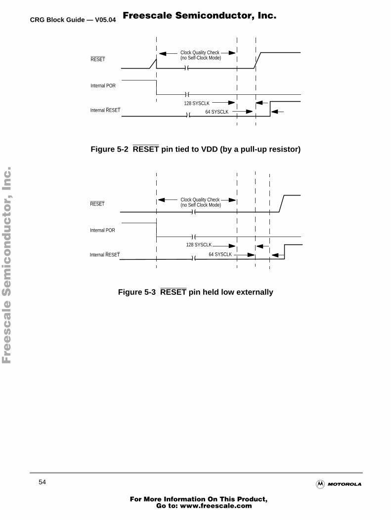
CRG Block Guide — V05.04
Fre
esc
ale
Se
mic
on
du
cto
r, I
Freescale Semiconductor, Inc.n
c..
.
Figure 5-2 RESET pin tied to VDD (by a pull-up resistor)
Figure 5-3 RESET pin held low externally
RESET
Internal POR
128 SYSCLK
64 SYSCLKInternal RESET
Clock Quality Check(no Self-Clock Mode)
) (
) (
) (
Clock Quality CheckRESET
Internal POR
Internal RESET
128 SYSCLK
64 SYSCLK
(no Self Clock Mode)) (
) (
) (
54
For More Information On This Product,
Go to: www.freescale.com

CRG Block Guide — V05.04
rruptsen a
ed for
frome
ged,able
resetre.
F
ree
sca
le S
em
ico
nd
uc
tor,
I
Freescale Semiconductor, Inc.n
c..
.
Section 6 Interrupts
6.1 General
The interrupts/reset vectors requested by the CRG are listed inTable 6-1 . Refer to MCU specification forrelated vector addresses and priorities.
6.2 Description of Interrupt Operation
6.2.1 Real Time Interrupt
The CRG generates a real time interrupt when the selected interrupt time period elapses. RTI inteare locally disabled by setting the RTIE bit to zero. The real time interrupt flag (RTIF) is set to1 whtimeout occurs, and is cleared to 0 by writing a 1 to the RTIF bit.
The RTI continues to run during Pseudo Stop Mode if the PRE bit is set to 1. This feature can be usperiodic wakeup from Pseudo Stop if the RTI interrupt is enabled.
6.2.2 PLL Lock Interrupt
The CRG generates a PLL Lock interrupt when the LOCK condition of the PLL has changed, eithera locked state to an unlocked state or vice versa. Lock interrupts are locally disabled by setting thLOCKIE bit to zero. The PLL Lock interrupt flag (LOCKIF) is set to1 when the LOCK condition haschanged, and is cleared to 0 by writing a 1 to the LOCKIF bit.
6.2.3 Self Clock Mode Interrupt
The CRG generates a Self Clock Mode interrupt when the SCM condition of the system has chaneither entered or exited Self Clock Mode. SCM conditions can only change if the Self Clock Mode enbit (SCME) is set to 1. SCM conditions are caused by a failing clock quality check after power on (POR) or low voltage reset (LVR) or recovery from Full Stop Mode (PSTP=0) or Clock Monitor failuFor details on the clock quality check refer to4.2.4 Clock Quality Checker. If the clock monitor isenabled (CME=1) a loss of external clock will also cause a SCM condition (SCME=1).
Table 6-1 CRG Interrupt Vectors
Interrupt Source CCRMask Local Enable
Real time interrupt I bit CRGINT (RTIE)
LOCK interrupt I bit CRGINT (LOCKIE)
SCM interrupt I bit CRGINT (SCMIE)
55
For More Information On This Product,
Go to: www.freescale.com
CRG Block Guide — V05.04
) is
F
ree
sca
le S
em
ico
nd
uc
tor,
I
Freescale Semiconductor, Inc.n
c..
.
SCM interrupts are locally disabled by setting the SCMIE bit to zero. The SCM interrupt flag (SCMIFset to1 when the SCM condition has changed, and is cleared to 0 by writing a 1 to the SCMIF bit.
56
For More Information On This Product,
Go to: www.freescale.com

CRG Block Guide — V05.04
Fre
esc
ale
Se
mic
on
du
cto
r, I
Freescale Semiconductor, Inc.n
c..
.
57
For More Information On This Product,
Go to: www.freescale.com

CRG Block Guide — V05.04
Fre
esc
ale
Se
mic
on
du
cto
r, I
Freescale Semiconductor, Inc.n
c..
.
FINAL PAGE OF58
PAGES
58
For More Information On This Product,
Go to: www.freescale.com