Embed Size (px)
Citation preview

AN:034 Page 1
Creating Higher Voltage Outputs Using Series Connected Sine Amplitude Converters
APPLICATION NOTE | AN:034
Introduction
The Sine Amplitude Converter (SAC) uses a zero current and zero voltage soft switching technique and fixed switching frequency in excess of 1MHz to provide fixed ratio DC-DC conversion. BCM® bus converters and VTM™ current multipliers are two important power components which use the SAC topology.
Most BCM and VTM products contain primary to secondary isolation. Because of this isolation, the outputs of isolated SACs may be connected in series. This enables the ability to create higher voltage outputs in both regulated and unregulated DC-DC systems. This application note explores several options for achieving this.
Sine Amplitude Converter Background
The SAC topology provides isolated, fixed ratio DC-DC conversion; the SAC output voltage (VOUT) is proportional to its input voltage (VIN) at no load per Equation 1.
In Equation 1, K is commonly referred to as the transformation ratio and is defined as the ratio of output voltage and input voltage. K is a fixed value for a given model of SAC.
The output voltage of a SAC follows Equation 2.
ROUT is a resistive term that is commonly referred to as the output resistance. ROUT is also constant for a given SAC, although the exact value will vary slightly with temperature.
While both employ the SAC topology, the BCM bus converter and VTM current multiplier have slightly different functions in a power system. The BCM is used to provide an isolated bus voltage from a narrow input voltage range DC source to power a downstream regulator. The VTM is used in Factorized Power Architecture™ systems in conjunction with PRM regulator to provide full DC-DC converter functionality. For more about Factorized Power Architecture, please refer to the following link: www.vicorpower.com/documents/whitepapers/fpa101.pdf.
(1)VOUT = K • VIN
(2)VOUT = K • VIN – IOUT • ROUT
Contents Page
Introduction 1
Sine Amplitude Converter Background 1
Series Connected Systems for Non-regulated DC-DC Conversion 2
Power, Voltage and Current Relationships 3
Startup Waveform for 50V to 200V Unregulated DC-DC Conversion 6
Series Connected Systems for Regulated DC-DC Conversion 9
Power, Voltage and Current Relationships 10
No Load Condition 10
Loaded Condition 10
Output Resistance 11
Compensating the Total Output Resistor of the Series Connected VTM Output 12
Trimming the PRM Output Voltage 12
Fault Control Circuits for Series Connected SAC Systems 13
Experimental Results Using Fault Management Circuits 16
General Considerations 18
Safety Considerations 18
LV BCMs and VTMs 19
HV BCMs 20
UHV BCMs 20
Conclusion 21
AN:034 Page 2
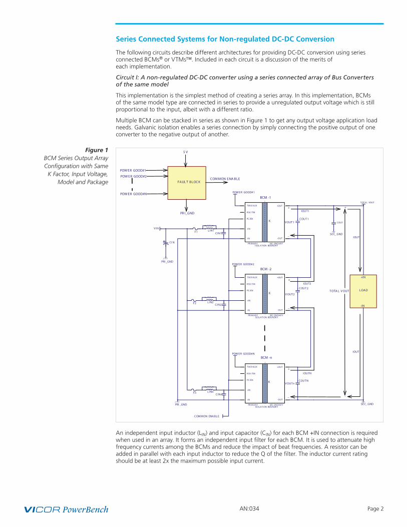
Series Connected Systems for Non-regulated DC-DC Conversion
The following circuits describe different architectures for providing DC-DC conversion using series connected BCMs® or VTMs™. Included in each circuit is a discussion of the merits of each implementation.
Circuit I: A non-regulated DC-DC converter using a series connected array of Bus Converters of the same model
This implementation is the simplest method of creating a series array. In this implementation, BCMs of the same model type are connected in series to provide a unregulated output voltage which is still proportional to the input, albeit with a different ratio.
Multiple BCM can be stacked in series as shown in Figure 1 to get any output voltage application load needs. Galvanic isolation enables a series connection by simply connecting the positive output of one converter to the negative output of another.
An independent input inductor (LIN) and input capacitor (CIN) for each BCM +IN connection is required when used in an array. It forms an independent input filter for each BCM. It is used to attenuate high frequency currents among the BCMs and reduce the impact of beat frequencies. A resistor can be added in parallel with each input inductor to reduce the Q of the filter. The inductor current rating should be at least 2x the maximum possible input current.
Figure 1 BCM Series Output Array Configuration with Same
K Factor, Input Voltage, Model and Package

AN:034 Page 3
When bus converters are connected in series output, additional output filtering is recommended, as the bus converters switching frequency are not synchronized. As well as an addition of the ripple voltages of multiple BCMs® in series array, the output could also produce relatively large beat frequencies. A capacitor (COUT) across the output of each BCM will help to attenuate the ripple. When an array is powering downstream regulators, LC filtering may be needed at the input of the regulators.
PC pin is enable pin in BCM. BCM enable pins must be connected together for startup synchronization. External capacitance on the enable bus is not permitted directly. All BCMs in the array must be enabled and disabled simultaneously. Control circuits can be added as needed to enable and disable the array using an external source and can be primary referenced or controlled from the secondary side using an opto-coupler. The BCM enable pin does not have pull down capability and thus external control circuits should be designed with this in mind. A fault control block is needed to insure that the series array of BCMs responds in an appropriate fashion to a fault. This block is discussed in detail in a future section.
The total output capacitance placed on the output of the BCM should be less than the maximum output capacitance as specified in the respective BCM datasheet. Be sure to include both the real capacitance at the output of each BCM in conjunction with the effective value of capacitance in series with the entire array. The total output capacitance for the system shown in Figure 1 is given by following Equation 3a.
Where COUT_TOTAL is total output capacticance of series connected system shown in Figure 1, COUTN is output capacticance of Nth BCM, N is the number of BCMs connected in series and COUT is output capacitance of series connected system.
Output capacitance per BCM is given by following Equation 3b.
BCMs can be paralleled at all N locations before their output connected in series to increase the output current of an array to meet the requirement of load.
Power, Voltage and Current Relationships
The total output voltage at no load for N BCMs connected in a series array output configuration is as follows:
Where KN is the transformation ratio for each series connected BCM, VOUTN is output voltage for each series connected BCM and VIN is the BCM input voltage.
For N identical BCMs, Equation 4 simplifies to:
Where N is the number of BCMs connected in series.
Due to ROUT the total output voltage is droops over load. Equation 6 gives the output voltage for series output array in loaded condition.
Again, for N identical BCMs this Equation can be simplified:
COUT_TOTAL = COUTN
N(3a)+ COUT
COUT_BCM = COUTN + N • COUT (3b)
N
Total_VOUT = ∑ VOUTN = (∑ KN) • VIN (4)N
N = 1 N = 1
Total_VOUT = N • VOUT = N • K • VIN (5)
N
Total_VOUT = (∑ KN) • VIN –IOUT • (∑ ROUTN) (6)N
N = 1 N = 1
Total_VOUT = N • (K • VIN – IOUT • ROUT) (7)

AN:034 Page 4
For N identical BCMs, efficiency of series output BCMs® array is same as efficiency of used single BCM for given output current and at fixed input voltage and fixed temperature. Data sheet efficiency charts can be used to determine the efficiency of series output BCMs array for given output current.
Example 1: A 50V to 200V unregulated DC-DC converter using series connected BCMs
Figure 2 shows a series connected array of 4 BCMs with K = 1 to create a 200V output. The system implemented as shown in Figure 2 is for 200V unregulated and isolated output voltage and provides 1200W output power at 50V input voltage. This system is implemented using four classic 48VIN BCMs (Bus Converter Modules). Classic 48VIN BCM has input voltage range of 38V to 55V. BCM with K factor of 1 provides 50V output voltage for 50V input voltage. Outputs of four such BCMs are connected in series to produce the 200V output voltage.
Figure 2 200V Output BCM Series Array
Configuration Using BCM with K Factor of 1, at 50V Input Voltage
and Same Model
AN:034 Page 5
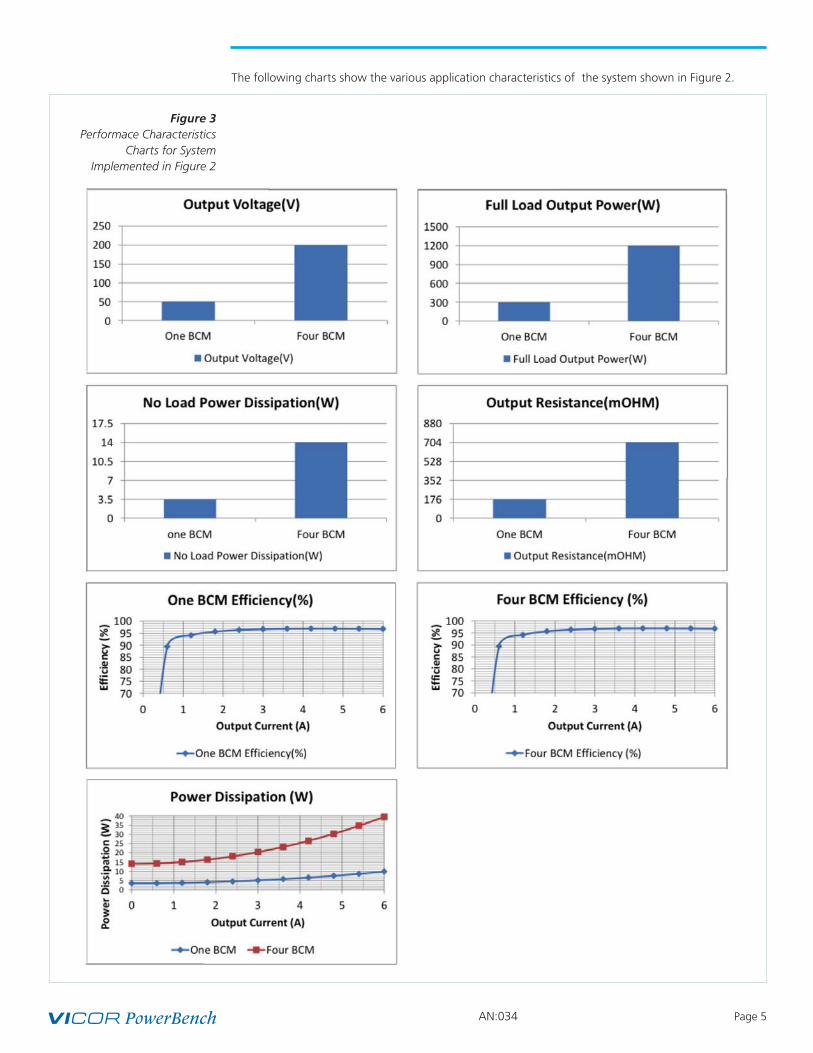
The following charts show the various application characteristics of the system shown in Figure 2.
Figure 3 Performace Characteristics
Charts for System Implemented in Figure 2

AN:034 Page 6
Startup Waveform for 50V to 200V Unregulated DC-DC Conversion
Startup upon application of input voltage
CH1: 50V Input Voltage
CH3: PC – Group Enable Signal
CH4: 200V Series Output Voltage
CH2: Output current
200V series output BCM® array is powering the resistive load
50V Input Voltage
197.1V Output voltage
Circuit II: A non-regulated DC-DC converter using a series connected array of Bus Converters with different K factors
Figure 5 shows an example array of bus converters with different K factors connected in a series array.
In this case there are some unique considerations that must be taken into account in addition to those mentioned for circuit I.
nn Turn on delay may be different for each BCM. BCM Enable pins must be connected together for startup synchronization. On/off control circuit can be added to sync the enable and disable of each BCM in the array using an external source. The load can be connected to BCM series output after array reaches its total output voltage to avoid the use of external diodes in startup condition. That means that load turn on is delayed to prevent the inrush type of startup issues.
nn The output current of any individual BCM in the series stack must not be exceeded. Refer to the product datasheet to insure that the appropriate current rating is not exceeded.
nn The fault management circuit should be implemented as described in future sections. If fault management circuit can not be implemented, then Schottky diodes are required to protect individual BCMs during asynchronous on/off times at startup or when one BCM shuts down for protection.
Figure 4 Startup Waveform
for System Implemented as Shown in Figure 2

AN:034 Page 7
Example 2: 48 to 28V unregulated DC-DC converter
To create a 28V output, one 24V output voltage BCM® with K factor of ½ can be connected in series with one 4V output voltage BCM with K factor of 1/12 as shown in Figure 6. In this case, the BCM with K factor of ½ is rated for a lower output current than the BCM with K factor of 1/12. Depending upon the total power requires BCMs with K factor of 1/2 can be paralleled before connecting their output in series with BCM with K factor of 1/12 to increase the total current capability of the array.
Figure 5 BCM Series Output Array
Configuration with Different K Factors
Figure 6 28V Output BCM Series Array Configuration using BCM with K Factor of ½ and BCM with a K Factor of 1/12, at 48V Input Voltage, Full VI Chip Package
and Different Model
Not applied COUT
100uF, 100 V AL EL
CIN 1
TOTA L VOUT
48 VIN0.1uHL IN1
1 Ohm20 A
F1
100uF, 100 VALEL
CIN 20.1uHL IN2
1 Ohm20 A
F2
SEC_GND
+IN
-I N
+OUT
-O UT
TM /V A UX
PC/EN
PRIM A RY SEC ONDA RYISOL A TION BOUNDRY
RSV /T M
BCM -1
+IN
-I N
+OUT
-O UT
TM /V A UX
PC/EN
PRIM A RY SEC ONDA RYISOL A TION BOUNDRY
RSV /T M
BCM -2
PRI _GND
PRI _GND SEC_GND
POWER GOOD #1
POW ER GOOD# 2
Not appliedCIN
8x1uF, 100V Ceramic
COU T1
8x47uF, 6.3V Ceramic
COU T2
V OUT1
V OUT2
TOTAL V OUT
+IN
-IN
L OA D
+
_
+
_
+IOUT1
IOUT2
IOU T
COMMON ENABLE
K =1/2
K =1/12
_
IOU T
24 V
4 V
28 V
28 V

AN:034 Page 8
Results
The following Equation provides the efficiency of N different BCMs® connected in series output.
For N identical BCMs, Equation 8 can be simplified to,
For two different BCMs as shown in Figure 6, Equation 8 can be simplified to,
Following Equation 11 can also be used as an alternate to Equation 8.
Table 1 below analyzes the efficiency of two series connected BCMs as shown in Figure 6 using Equation 8 at 48V input voltage to BCMs, 12.5A output current and 25°C temperature.
ηTOTAL = (8)
N
∑ N = 1
POUTN N
∑ N = 1
POUTN ηN
(9)ηTOTAL = η
(10)ηTOTAL = POUT1 + POUT2
+ POUT1η1
POUT2η2
(11)
N
∑ N = 1
POUTN N
∑ N = 1
POUTN + N∑ N = 1
PNL N
∑ N = 1
I 2OUT • (ROUTN)+
From Data Sheet or
Whiteboard
Using Equation 2
From Data Sheet or
Whiteboard
BCMROUT at 25°C
in (mΩ)Output Voltage
VOUT (V)Output Power
POUT (W)Efficiency (%)
Input Power PIN (W)
K = 1/2 Full VI Chip 47.5 23.406 292.6 95.5 306.4
K = 1/12 Full VI Chip 2.5 3.969 49.6 91 54.5
Total Output Voltage (V) 27.375
Total Output Power (W) 342.2
Total Input Power (W) 360.9
Total Efficiency (%) 94.82
Table 1
AN:034 Page 9
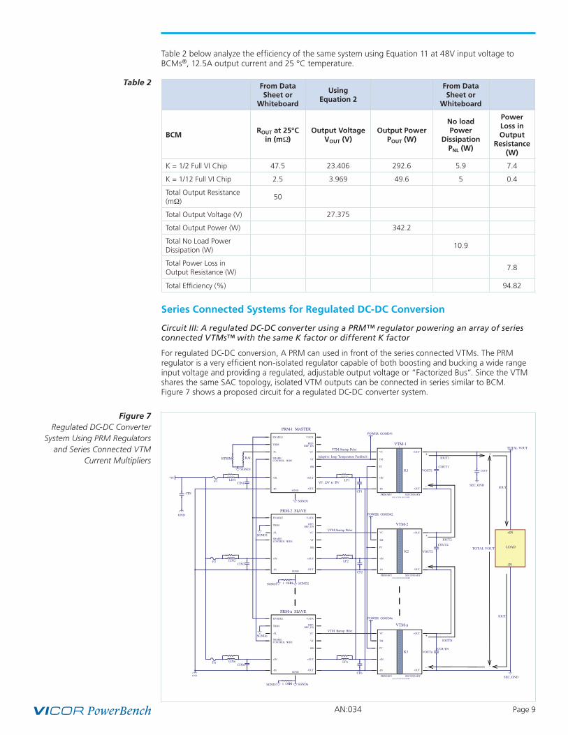
Table 2 below analyze the efficiency of the same system using Equation 11 at 48V input voltage to BCMs®, 12.5A output current and 25 °C temperature.
Series Connected Systems for Regulated DC-DC Conversion
Circuit III: A regulated DC-DC converter using a PRM™ regulator powering an array of series connected VTMs™ with the same K factor or different K factor
For regulated DC-DC conversion, A PRM can used in front of the series connected VTMs. The PRM regulator is a very efficient non-isolated regulator capable of both boosting and bucking a wide range input voltage and providing a regulated, adjustable output voltage or “Factorized Bus”. Since the VTM shares the same SAC topology, isolated VTM outputs can be connected in series similar to BCM. Figure 7 shows a proposed circuit for a regulated DC-DC converter system.
Figure 7 Regulated DC-DC Converter
System Using PRM Regulators and Series Connected VTM
Current Multipliers
From Data Sheet or
Whiteboard
Using Equation 2
From Data Sheet or
Whiteboard
BCMROUT at 25°C
in (mΩ)Output Voltage
VOUT (V)Output Power
POUT (W)
No load Power
Dissipation PNL (W)
Power Loss in Output
Resistance (W)
K = 1/2 Full VI Chip 47.5 23.406 292.6 5.9 7.4
K = 1/12 Full VI Chip 2.5 3.969 49.6 5 0.4
Total Output Resistance (mΩ)
50
Total Output Voltage (V) 27.375
Total Output Power (W) 342.2
Total No Load Power Dissipation (W)
10.9
Total Power Loss in Output Resistance (W)
7.8
Total Efficiency (%) 94.82
VTM Startup Pulse
Adaptive Loop Temperature Feedback
VF: 20V to 55VLF1
RALRTRIM
CF1
CIN1
TRIM
AL
+IN
-IN
+OUT
-OUT
VC
IFB
VT
REF/REF_EN
VAUX
SHARE/CONTROL NODE
ENABLE
SGND
PRM-1 MASTER
SGND1
SGND1
VINLIN1F1
VTM Startup Pulse
LF2
CF2
CIN2
TRIM
AL
+IN
-IN
+OUT
-OUT
VC
IFB
VT
REF/REF_EN
VAUX
SHARE/CONTROL NODE
ENABLE
SGND
PRM-2 SLAVE
SGND2
LIN2F2
+IN
-IN
+OUT
-OUT
VC
PC
PRIMARY SECONDARYISOLATION BOUNDRY
TM
VTM-1
+IN
-IN
+OUT
-OUT
VC
PC
PRIMARY SECONDARYISOLATION BOUNDRY
TM
VTM-2
1 OHM
CIN
GND
SGND1 SGND2
VTM Startup Pulse
LFn
CFn
CINn
GND
TRIM
AL
+IN
-IN
+OUT
-OUT
VC
IFB
VT
REF/REF_EN
VAUX
SHARE/CONTROL NODE
ENABLE
SGND
PRM-n SLAVE
SGNDn
LINnFn+IN
-IN
+OUT
-OUT
VC
PC
PRIMARY SECONDARYISOLATION BOUNDRY
TM
VTM-n
1 OHMSGND1 SGNDn
COUT
TOTAL VOUT
SEC_GND
SEC_GND
COUT1
COUT2
COUTN
VOUT1
VOUT2
VOUTn
TOTAL VOUT
+IN
-IN
LOAD
+
_
+
_
+
_
+
_
IOUT1
IOUT2
IOUTN
IOUT
IOUT
POWER GOOD#1
POWER GOOD#2
POWER GOOD#n
K1
K2
K3
Table 2

AN:034 Page 10
Power, Voltage and Current Relationships
Key relationships to be considered for adaptive loop are the following for N identical VTM™ models connected to series output.
No Load Condition
Total output voltage is a sum of output voltage given by all VTMs connected in series output at no load condition.
Where KN is the transformation ratio for each series connected VTM and N is the number of VTMs in series output array and VF is the PRM™ output voltage, which is VTM input voltage.
For N identical VTMs this simplifies to:
The series array configuration results in a new K factor which is defined as:
For N identical VTMs, this simplifies to:
Loaded Condition
The VTM is modeled as pure resistive impedance. Total output voltage is droop due to the small output resistance introduced by VTM in loaded condition. The following equation gives the output voltage for series output array in loaded condition.
For N identical VTMs connected in series, this simplifies to:
N
∑ N = 1
Total_VOUT = (12)N
∑ N = 1
VOUTN = ( KN) • VIN
Total_VOUT = N • VOUT = N • K • VF(13)
(14)KNEW = = N∑ N = 1
KN Total_VOUT
VF
= N
∑ N = 1
( KN) • VF
VF
(16)N
∑ N = 1
( KN) • VF – IOUT • Total_VOUT = N
∑ N = 1
( ROUT)
Total_VOUT = N • (K • VF – IOUT • ROUT ) (17)
(15)KNEW = N • K

AN:034 Page 11
Output Resistance
For N identical VTMs™, this simplifies to
Total output resistance referred to the VTM input side:
For N identical VTMs, this simplifies to
Example 4: A 48V to 72V regulated DC-DC converter using series connected VTMs and PRMs
ROUT_TOTAL = (18)ROUTN N
∑ N = 1
ROUT_TOTAL = N • ROUT (19)
ROUT_REFL = (20)ROUT_TOTAL (KNEW)2
ROUT_REFL = (21)ROUT N • K2
Figure 8 72V Isolated and Regulated
Output Voltage Using the PRM™ and Series Connected
VTMs with Same K Factor and Model
VTM Startup Pulse
Adaptive Loop Temperature Feedback
VF: 48 V LF1
RALRTRIM
CF1
CIN1
TRIM
AL
+IN
-IN
+OUT
-OUT
VC
IFB
VT
REF/REF_EN
VAUX
SHARE/CONTROL NODE
ENABLE
SGND
PRM-1 MASTER
SGND1
SGND1
VINLIN1F1
VTM Startup Pulse
LF2
CF2
CIN2
TRIM
AL
+IN
-IN
+OUT
-OUT
VC
IFB
VT
REF/REF_EN
VAUX
SHARE/CONTROL NODE
ENABLE
SGND
PRM-2 SLAVE
SGND2
LIN2F2
+IN
-IN
+OUT
-OUT
VC
PC
PRIMARY SECONDARYISOLATION BOUNDRY
TM
VTM-1
+IN
-IN
+OUT
-OUT
VC
PC
PRIMARY SECONDARYISOLATION BOUNDRY
TM
VTM-2
1 OHM
CIN
GND
SGND1 SGND2
VTM Startup Pulse
LF3
CF3
CIN3
GND
TRIM
AL
+IN
-IN
+OUT
-OUT
VC
IFB
VT
REF/REF_EN
VAUX
SHARE/CONTROL NODE
ENABLE
SGND
PRM-3 SLAVE
SGND3
LIN3F3+IN
-IN
+OUT
-OUT
VC
PC
PRIMARY SECONDARYISOLATION BOUNDRY
TM
VTM-3
1 OHMSGND1 SGNDn
COUT
TOTAL VOUT
SEC_GND
SEC_GND
COUT1
COUT2
COUT3
VOUT1
VOUT2
VOUT3
TOTAL VOUT
+IN
-IN
LOAD
+
_
+
_
+
_
+
_
IOUT1
IOUT2
IOUT3
IOUT
IOUT
POWER GOOD#1
POWER GOOD#2
POWER GOOD#3
K=1/2
K=1/2
K=1/2
24 V
24 V
24 V
72 V
72 V

AN:034 Page 12
The system implemented as shown in Figure 8 is for 72V regulated and isolated output voltage and provides 864W output power at 12A load current and 48V unregulated input voltage. This system is implemented using three Buck-boost PRMs™ (Pre-Regulator Modules) in parallel and three classic 48VIN VTMs™ (Voltage Transformation Modules). 48VIN classic VTM has input voltage range of 26V to 55V. VTM with K factor of ½ provides 24V output voltage for 48V factorize bus voltage. Outputs of three such VTMs are connected in series to produce the 72V output voltage. Three 400W rated PRMs are connected in parallel using master-slave operation. Each PRM has nominal input voltage of 48V and accepts wide input voltage range from 36V to 75V. In paralleling of PRMs, one PRM is configured as MASTER and rest are configured as slave. Master PRM output voltage is set at 48V to match the required factorise bus. PRM output voltage is adaptively increased with the increase in load current to regulate the VTM output voltage by compensating the output voltage droop due to total output resistance of series connected VTMs.
For the example shown in Figure 8, ROUT_TOTAL is 142.5mΩ at 25°C, per Equation 18, KNEW is 3/2 per Equation 14.
Compensating the Total Output Resistor of the Series Connected VTM Output
1. Calculate the total output reistance of series connected VTMs at 25 °C using Equation 18. (ROUT_TOTAL_25C)
2. Calcualte the new K factor of series connected VTMs using Equation 14. (KNEW)
3. Calculate the reflected output resistance of the VTMs (ROUT_REFL) using Equation 20 and using new variables (ROUT_TOTAL_25C for ROUT_VTM_25C) and (KNEW for K) refer to adaptive loop operation section in configurable PRM data sheet.
4. Determine the number of PRMs required. Calculate the compensation slope (RLL_AL) from reflected output resistance of the VTMs and number of PRMs.
5. Calculate the voltage on the AL pin using Equation 3 refer to adaptive loop section in configurable PRM data sheet.
6. Calculate AL resistor (RAL) using Equation 4 refer to adaptive loop section in configurable PRM data sheet.
7. Adaptive loop temperature compensation refer to adaptive loop operation in configurable PRM data sheet.
Trimming the PRM Output Voltage
1. Determine the number of VTMs required for series connected VTMs with appropriate K factor.
2. Calculate the PRM output voltage required at no load from total output voltage of series connected VTMs and new K factor KNEW using Equation 14.
3. Calculate the voltage on the Trim pin using Equation 1; refer to Adaptive Loop Operation in configurable PRM data sheet.
4. Calculate Trim resistor (RTRIM) using Equation 1; refer to Adaptive Loop Operation in configurable PRM data sheet.
RLL_AL = NPRMs • ROUT_REFL (22)
AN:034 Page 13
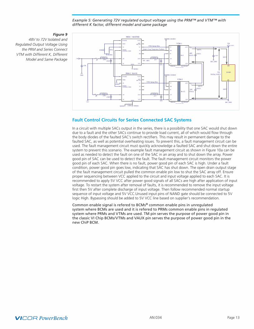
Example 5: Generating 72V regulated output voltage using the PRM™ and VTM™ with different K factor, different model and same package
Fault Control Circuits for Series Connected SAC Systems
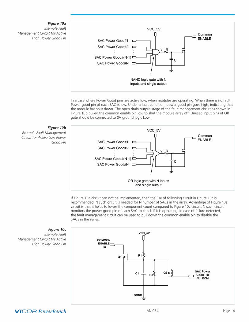
In a circuit with multiple SACs output in the series, there is a possibility that one SAC would shut down due to a fault and the other SACs continue to provide load current, all of which would flow through the body diodes of the faulted SAC’s switch rectifiers. This may result in permanent damage to the faulted SAC, as well as potential overheating issues. To prevent this, a fault management circuit can be used. The fault management circuit must quickly acknowledge a faulted SAC and shut down the entire system to prevent this scenario. The example fault management circuit as shown in Figure 10a can be used as needed to detect the fault on one of the SAC in an array and to shut down the array. Power good pin of SAC can be used to detect the fault. The fault management circuit monitors the power good pin of each SAC. When there is no fault, power good pin of each SAC is high. Under a fault condition, power good pin goes low, indicating that SAC has shut down. The open drain output stage of the fault management circuit pulled the common enable pin low to shut the SAC array off. Ensure proper sequencing between VCC applied to the circuit and input voltage applied to each SAC. It is recommended to apply 5V VCC after power good signals of all SACs are high after application of input voltage. To restart the system after removal of faults, it is recommended to remove the input voltage first then 5V after complete discharge of input voltage. Then follow recommended normal startup sequence of input voltage and 5V VCC.Unused input pins of NAND gate should be connected to 5V logic High. Bypassing should be added to 5V VCC line based on supplier’s recommendation.
Common enable signal is refered to BCMs® common enable pins in unregulated system where BCMs are used and it is refered to PRMs common enable pins in regulated system where PRMs and VTMs are used. TM pin serves the purpose of power good pin in the classic VI Chip BCMs/VTMs and VAUX pin serves the purpose of power good pin in the new ChiP BCM.
Figure 9 48V to 72V Isolated and
Regulated Output Voltage Using the PRM and Series Connect
VTM with Different K, Different Model and Same Package
VTM Startup Pulse
Adaptive Loop Temperature Feedback
VF: 48 V LF1
RALRTRIM
CF1
CIN1
TRIM
AL
+IN
-IN
+OUT
-OUT
VC
IFB
VT
REF/REF_EN
VAUX
SHARE/CONTROL NODE
ENABLE
SGND
PRM-1 MASTER
SGND1
SGND1
VINLIN1F1
VTM Startup Pulse
LF2
CF2
CIN2
TRIM
AL
+IN
-IN
+OUT
-OUT
VC
IFB
VT
REF/REF_EN
VAUX
SHARE/CONTROL NODE
ENABLE
SGND
PRM-2 SLAVE
SGND2
LIN2F2
+IN
-IN
+OUT
-OUT
VC
PC
PRIMARY SECONDARYISOLATION BOUNDRY
TM
VTM-1
+IN
-IN
+OUT
-OUT
VC
PC
PRIMARY SECONDARYISOLATION BOUNDRY
TM
VTM-2
1 OHM
CIN
GND
SGND1 SGND2
GND
POWER GOOD#1
POWER GOOD#2
K=1
K=1/2
COUT
TOTAL VOUT
SEC_GND
SEC_GND
COUT1
COUT2
VOUT1
VOUT2
TOTAL VOUT
+IN
-IN
LOAD
+
_
+
_
+IOUT1
IOUT2
IOUT
_
IOUT
48 V
24 V
72 V
72 V
AN:034 Page 14
In a case where Power Good pins are active low, when modules are operating. When there is no fault, Power good pin of each SAC is low. Under a fault condition, power good pin goes high, indicating that the module has shut down. The open drain output stage of the fault management circuit as shown in Figure 10b pulled the common enable pin low to shut the module array off. Unused input pins of OR gate should be connected to 0V ground logic Low.
If Figure 10a circuit can not be implemented, then the use of following circuit in Figure 10c is recommended. N such circuit is needed for N number of SACs in the array. Advantage of Figure 10a circuit is that it helps to lower the component count compared to Figure 10c circuit. N such circuit monitors the power good pin of each SAC to check if it is operating. In case of failure detected, the fault management circuit can be used to pull down the common enable pin to disable the SACs in the series.
Figure 10a Example Fault
Management Circuit for Active High Power Good Pin
Figure 10b Example Fault Management Circuit for Active Low Power
Good Pin
Figure 10c Example Fault
Management Circuit for Active High Power Good Pin

AN:034 Page 15
If the fault management circuit can’t be implemented, then Schottky diodes are required to protect individual SACs during asynchronous on/off times or when one SAC shuts down for protection. A lower forward bias (VF) Schottky diode can be added at the output of each SAC with the cathode connected to +OUT and anode connected to –OUT as shown in Figure 11 to bypass the current flowing through the body diode of the output MOSFETs and secondary winding of transformer of SAC topology in case of a fault on one of the SAC in the array. The Schottky’s (VF) is far less than that of the PN junction rectifiers (body diodes). Thus, the Schottky conducts the current instead of body diode. This diode must have a reverse voltage rating greater than the SAC’s maximum possible output voltage and a forward current rating greater than the array’s maximum possible load current.
Figure 11 Showing Schottky Protection Diode
AN:034 Page 16
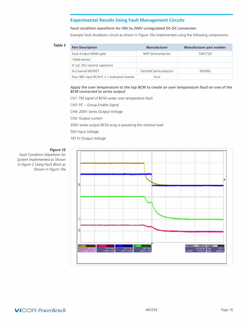
Experimental Results Using Fault Management Circuits
Fault condition waveform for 50V to 200V unregulated DC-DC conversion
Example fault shutdown circuit as shown in Figure 10a implemented using the following components.
Apply the over temperature to the top BCM to create an over temperature fault on one of the BCM connected to series output
CH1: TM signal of BCM under over temperature fault
CH3: PC – Group Enable Signal
CH4: 200V Series Output Voltage
CH2: Output current
200V series output BCM array is powering the resistive load
50V Input Voltage
197.1V Output Voltage
Figure 12 Fault Condition Waveform for
System Implemented as Shown in Figure 2 Using Fault Block as
Shown in Figure 10a
Part Description Manufacturer Manufacturer part number
Dual 4-input NAND gate NXP Semiconductor 74HCT20
10kΩ resistor
0.1µF, 25V ceramic capacitors
N-Channel MOSFET Fairchild Semiconductor 2N7000
Four 48V input BCM K = 1 evaluation boards Vicor
Table 3
AN:034 Page 17
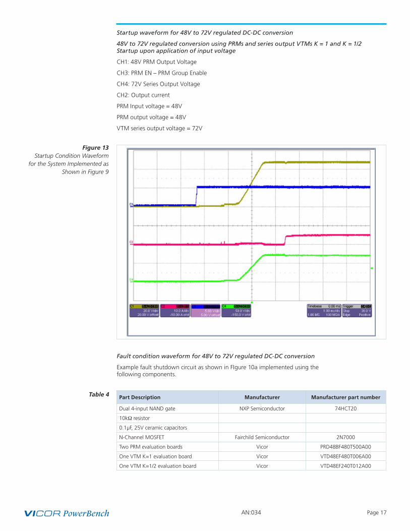
Startup waveform for 48V to 72V regulated DC-DC conversion
48V to 72V regulated conversion using PRMs and series output VTMs K = 1 and K = 1/2 Startup upon application of input voltage
CH1: 48V PRM Output Voltage
CH3: PRM EN – PRM Group Enable
CH4: 72V Series Output Voltage
CH2: Output current
PRM Input voltage = 48V
PRM output voltage = 48V
VTM series output voltage = 72V
Fault condition waveform for 48V to 72V regulated DC-DC conversion
Example fault shutdown circuit as shown in FIgure 10a implemented using the following components.
Figure 13 Startup Condition Waveform
for the System Implemented as Shown in Figure 9
Part Description Manufacturer Manufacturer part number
Dual 4-input NAND gate NXP Semiconductor 74HCT20
10kΩ resistor
0.1µF, 25V ceramic capacitors
N-Channel MOSFET Fairchild Semiconductor 2N7000
Two PRM evaluation boards Vicor PRD48BF480T500A00
One VTM K=1 evaluation board Vicor VTD48EF480T006A00
One VTM K=1/2 evaluation board Vicor VTD48EF240T012A00
Table 4
AN:034 Page 18
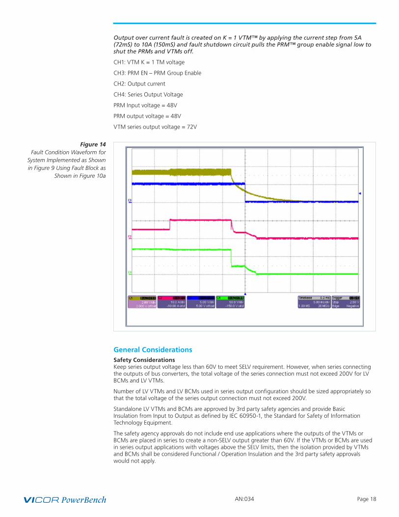
Output over current fault is created on K = 1 VTM™ by applying the current step from 5A (72mS) to 10A (150mS) and fault shutdown circuit pulls the PRM™ group enable signal low to shut the PRMs and VTMs off.
CH1: VTM K = 1 TM voltage
CH3: PRM EN – PRM Group Enable
CH2: Output current
CH4: Series Output Voltage
PRM Input voltage = 48V
PRM output voltage = 48V
VTM series output voltage = 72V
General ConsiderationsSafety ConsiderationsKeep series output voltage less than 60V to meet SELV requirement. However, when series connecting the outputs of bus converters, the total voltage of the series connection must not exceed 200V for LV BCMs and LV VTMs.
Number of LV VTMs and LV BCMs used in series output configuration should be sized appropriately so that the total voltage of the series output connection must not exceed 200V.
Standalone LV VTMs and BCMs are approved by 3rd party safety agencies and provide Basic Insulation from Input to Output as defined by IEC 60950-1, the Standard for Safety of Information Technology Equipment.
The safety agency approvals do not include end use applications where the outputs of the VTMs or BCMs are placed in series to create a non-SELV output greater than 60V. If the VTMs or BCMs are used in series output applications with voltages above the SELV limits, then the isolation provided by VTMs and BCMs shall be considered Functional / Operation Insulation and the 3rd party safety approvals would not apply.
Figure 14 Fault Condition Waveform for
System Implemented as Shown in Figure 9 Using Fault Block as
Shown in Figure 10a

AN:034 Page 19
LV BCMs and VTMs (48VIN Classic VI Chip BCMs/VTMs, 36VIN Classic VI ChiP MVTMs and New 48VIN ChiP and VIA BCMs)
The input to the VTMs and BCMs is intended to be supplied from a TNV-2 nonhazardous secondary circuit. When supplied by a TNV-2 circuit, the output of the VTMs and BCMs can be considered SELV. The isolation (Basic Insulation) provided by the VTMs and BCMs has a maximum rated dielectric withstand capability of 2250VDC.
48V input isolated BCMs and VTMs can be series connected to produce output voltages of up to positive 200V. Safety agency approvals are the user’s responsibility for systems where the total series connection voltage exceeds 60V.
For functional and reliability purposes, a hazardous secondary output created by the series array shall not exceed 200VDC and voltage between any pair of terminals of any stacked VTMs and BCMs shall not exceed 200V, refer to Figure 11. For end use applications with series array output voltages between 60V and 200V, the VTMs and BCMs provide Functional / Operational Insulation and the input shall also be considered a hazardous secondary circuit at a potential equivalent to the serial output.
Figure11a Conditions for LV BCMs and
VTMs Connected in Series Output Stack
LV BCMs and VTMsFigure11b Conditions for LV BCMs and
VTMs Connected in Series Output Stack
AN:034 Page 20
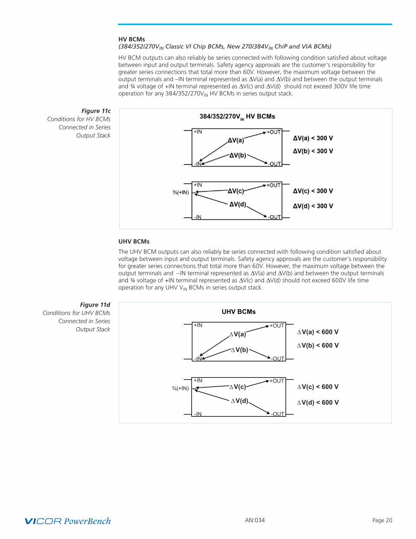
HV BCMs (384/352/270VIN Classic VI Chip BCMs, New 270/384VIN ChiP and VIA BCMs)
HV BCM outputs can also reliably be series connected with following condition satisfied about voltage between input and output terminals. Safety agency approvals are the customer’s responsibility for greater series connections that total more than 60V. However, the maximum voltage between the output terminals and –IN terminal represented as ΔV(a) and ΔV(b) and between the output terminals and ¾ voltage of +IN terminal represented as ΔV(c) and ΔV(d) should not exceed 300V life time operation for any 384/352/270VIN HV BCMs in series output stack.
UHV BCMs
The UHV BCM outputs can also reliably be series connected with following condition satisfied about voltage between input and output terminals. Safety agency approvals are the customer's responsibility for greater series connections that total more than 60V. However, the maximum voltage between the output terminals and –IN terminal represented as ΔV(a) and ΔV(b) and between the output terminals and ¾ voltage of +IN terminal represented as ΔV(c) and ΔV(d) should not exceed 600V life time operation for any UHV VIN BCMs in series output stack.
Figure 11c Conditions for HV BCMs
Connected in Series Output Stack
384/352/270VIN HV BCMs
Figure 11d Conditions for UHV BCMs
Connected in Series Output Stack
+OUT
-OUT
+IN
-IN
+OUT
-OUT
+IN
-IN
∆V(a)
∆V(b)
¾(+IN) ∆V(c)
∆V(d)
∆V(a) < 600 V
∆V(b) < 600 V
∆V(c) < 600 V
∆V(d) < 600 V
UHV BCMsUHV BCMs
AN:034 Page 21
Table 5 provides few examples to illustrate an acceptable and non-acceptable real world system considering a single point ground system.
Conclusion
The sine amplitude converter family has LV BCMs and VTMs (48VIN Classic VI Chip BCMs/VTMs, 36VIN Classic VI ChiP MVTMs and new 48VIN ChiP and VIA BCMs), HV BCMs (384/352/270VIN Classic VI Chip BCMs, new 270/384VIN ChiP and VIA BCMs) and UHV BCMs with a set of standard K factors. Sine Amplitude Converter outputs can be connected in series to generate different non-standard K factor to create a higher voltage outputs to meet requirements of various applications in unregulated and regulated DC-DC systems.
Acceptable real world system Non-accepatable real world system
Generating a positive 200V output from 50V input is acceptable using classic 48VIN BCMs and VTMs™
Generating a negative 200V output from 50V input is not acceptable using classic 48VIN BCMs and VTMs
Generating a negative 150V from 50V input is acceptable using classic 48VIN VTMs and BCMs
Generating a positive 24V output from 384V input is acceptable using 384VIN BCMs.
Generating a negative 24V output from 384V input is not acceptable using BCMs
Generating a ±120V regulated output from 48V input using PRMs and VTMs is acceptable
Generating ±160V output from 40V input is acceptable using VTMs and BCMs
Generating a ±170V regulated output from 48V input using PRMs™ and VTMs is not acceptable
Table 5

08/17 Rev 1.1 Page 22
Limitation of WarrantiesInformation in this document is believed to be accurate and reliable. HOWEVER, THIS INFORMATION IS PROVIDED “AS IS” AND WITHOUT ANY WARRANTIES, EXPRESSED OR IMPLIED, AS TO THE ACCURACY OR COMPLETENESS OF SUCH INFORMATION. VICOR SHALL HAVE NO LIABILITY FOR THE CONSEQUENCES OF USE OF SUCH INFORMATION. IN NO EVENT SHALL VICOR BE LIABLE FOR ANY INDIRECT, INCIDENTAL, PUNITIVE, SPECIAL OR CONSEQUENTIAL DAMAGES (INCLUDING, WITHOUT LIMITATION, LOST PROFITS OR SAVINGS, BUSINESS INTERRUPTION, COSTS RELATED TO THE REMOVAL OR REPLACEMENT OF ANY PRODUCTS OR REWORK CHARGES).
Vicor reserves the right to make changes to information published in this document, at any time and without notice. You should verify that this document and information is current. This document supersedes and replaces all prior versions of this publication.
All guidance and content herein are for illustrative purposes only. Vicor makes no representation or warranty that the products and/or services described herein will be suitable for the specified use without further testing or modification. You are responsible for the design and operation of your applications and products using Vicor products, and Vicor accepts no liability for any assistance with applications or customer product design. It is your sole responsibility to determine whether the Vicor product is suitable and fit for your applications and products, and to implement adequate design, testing and operating safeguards for your planned application(s) and use(s).
VICOR PRODUCTS ARE NOT DESIGNED, AUTHORIZED OR WARRANTED FOR USE IN LIFE SUPPORT, LIFE-CRITICAL OR SAFETY-CRITICAL SYSTEMS OR EQUIPMENT. VICOR PRODUCTS ARE NOT CERTIFIED TO MEET ISO 13485 FOR USE IN MEDICAL EQUIPMENT NOR ISO/TS16949 FOR USE IN AUTOMOTIVE APPLICATIONS OR OTHER SIMILAR MEDICAL AND AUTOMOTIVE STANDARDS. VICOR DISCLAIMS ANY AND ALL LIABILITY FOR INCLUSION AND/OR USE OF VICOR PRODUCTS IN SUCH EQUIPMENT OR APPLICATIONS AND THEREFORE SUCH INCLUSION AND/OR USE IS AT YOUR OWN RISK.
Terms of SaleThe purchase and sale of Vicor products is subject to the Vicor Corporation Terms and Conditions of Sale which are available at: (http://www.vicorpower.com/termsconditionswarranty)
Export ControlThis document as well as the item(s) described herein may be subject to export control regulations. Export may require a prior authorization from U.S. export authorities.
Contact Us: http://www.vicorpower.com/contact-us
Vicor Corporation25 Frontage Road
Andover, MA, USA 01810Tel: 800-735-6200Fax: 978-475-6715
www.vicorpower.com
emailCustomer Service: [email protected]
Technical Support: [email protected]
©2017 Vicor Corporation. All rights reserved. The Vicor name is a registered trademark of Vicor Corporation.All other trademarks, product names, logos and brands are property of their respective owners.