Embed Size (px)
Citation preview

Mohd Uzir Kamaluddin / Feb 2020 Page 1
COURSE / CODE DIGITAL ELECTRONICS FUNDAMENTAL (ECE422)
PROGRAMMABLE LOGIC DEVICES (PLDs)
A PLD, or programmable logic device, is an electronic component that is used in order to build
digital circuits that are reprogrammable. A programmable logic device does not have a defined
function once manufactured, unlike a logic gate and has to be programmed before it can be used.
Programmable logic devices (PLD) are designed with
configurable logic and flip-flops linked together with
programmable interconnect.
PLDs provide specific functions, including device-to-device
interfacing, data communication, signal processing, data display,
timing and control operations, and almost every other function a
system must perform. Memory cells control and define the
function that the logic performs and how the various logic
functions are interconnected.
FPGAs are used in a wide variety of applications ranging from
data processing and storage, to instrumentation, telecommunications, and digital signal
processing. CPLDs, by contrast, offer much smaller amounts of logic - up to about 10,000 gates.
But CPLDs offer very predictable timing characteristics and are therefore ideal for critical control
applications.
Some CPLDs require extremely low amounts of power and are very inexpensive, making them
ideal for cost-sensitive, battery-operated, portable applications such as mobile phones and digital
handheld assistants.
Categories
Logic devices can be classified into two broad categories - fixed and programmable.
Fixed Logic Devices
As the name suggests, the circuits in a fixed logic device are permanent, they perform one
function or set of functions - once manufactured, they cannot be changed.
With fixed logic devices, the time required to go from design, to prototypes, to a final
manufacturing run can take from several months to more than a year, depending on the
complexity of the device. And, if the device does not work properly, or if the requirements
change, a new design must be developed.

Mohd Uzir Kamaluddin / Feb 2020 Page 2
Programmable Logic Devices
On the other hand, programmable logic devices (PLDs) are
standard, off-the-shelf parts that offer customers a wide range of
logic capacity, features, speed, and voltage characteristics - and
these devices can be changed at any time to perform any number
of functions.
With programmable logic devices, designers use inexpensive
software tools to quickly develop, simulate, and test their
designs. Then, a design can be quickly programmed into a
device, and immediately tested in a live circuit. The PLD that is
used for this prototyping is the exact same PLD that will be used in the final production of a piece
of end equipment, such as a network router, a DSL modem, a DVD player, or an automotive
navigation system. There are no NRE costs and the final design is completed much faster than
that of a custom, fixed logic device.
Another key benefit of using PLDs is that during the design phase customers can change the
circuitry as often as they want until the design operates to their satisfaction. That's because PLDs
are based on re-writeable memory technology - to change the design, simply reprogram the
device. Once the design is final, customers can go into immediate production by simply
programming as many PLDs as they need with the final software design file.
Types
Generally, programmable logic devices can be described as being one of three different types:
Simple programmable logic devices (SPLD)
Complex programmable logic devices (CPLD)
Field programmable logic devices (FPGA)
Architecture
There are several manufacturers with many different families of PLD devices, so there are many
variations in architecture. The two major types of programmable logic devices are:
Field programmable gate arrays (FPGAs)
Complex programmable logic devices (CPLDs)
The distinction between the two is often a little fuzzy, with manufacturers designing new,
improved architectures, and frequently muddying the waters for marketing purposes. Together,
CPLDs and FPGAs are often referred to as high-capacity programmable logic devices (HCPLD).
Simple Programmable Logic Devices (SPLD)
Simple programmable logic devices (SPLD) are the simplest, smallest and least-expensive forms
of programmable logic devices. SPLDs can be used in boards to replace 7400-series TTL
components (AND, OR, and NOT gates).
Simple programmable logic devices typically comprise 4 to 22 fully connected macrocells. These
macrocells are typically comprised of some combinatorial logic (such as AND OR gates) and
a flip-flop. In other words, a small Boolean logic equation can be built within each macrocell. This
equation will combine the state of some number of binary inputs into a binary output and, if
necessary, store that output in the flip-flop until the next clock edge. Of course, the particulars of
the available logic gates and flip-flops are specific to each manufacturer and product family. But
the general idea is always the same.
Most SPLDs use either fuses or non-volatile memory cells (EPROM, EEPROM, FLASH, and
others) to define the functionality.

Mohd Uzir Kamaluddin / Feb 2020 Page 3
These devices are also known as:
Programmable array logic (PAL)
Generic array logic (GAL)
Programmable logic arrays (PLA)
Field-programmable logic arrays (FPLA)
Programmable logic devices (PLD)
Advantages
PLDs are often used for address decoding, where they have several clear advantages over the
7400-series TTL parts that they replaced:
1. One chip requires less board area, power, and wiring than several do.
2. The design inside the chip is flexible, so a change in the logic does not require any
rewiring of the board. Rather, simply replacing one PLD with another part that has
been programmed with the new design can alter the decoding logic.
Functions
Programmable Logic Devices (PLDs) are digital devices with configurable logic and flip-flops
linked together with programmable interconnect. Logic devices provide specific functions,
including:
Device-to-device interfacing
Data communication
Signal processing
Data display
Timing
Control operations
Almost every other function a
system must perform
Memory cells control and define the function that the logic performs and how the various logic
functions are interconnected.
Programming Technology
The programming technologies for PLD devices are based on the various types of semiconductor
memory. As new types of memories have been developed, the same technology has been applied
to the creation of new types of PLD devices.
The amount of logic resources available is the major distinguishing feature between SPLDs and
HCPLDs. Today, SPLDs are devices that typically contain the equivalent of 600 or fewer gates,
while HCPLDs have thousands and hundreds of thousands of gates available.
Of the two types of HCPLD devices, FPGAs offer the highest amount of logic density, the most
features, and the highest performance.
Examples of PLD applications
There are many applications that use programmable logic devices including in the field of:
Networking
Aerospace and defense
Automotive
Consumer electronics
Computing
Distributed monetary systems
Communications
Audio
Computing
Avionics
Some small scale applications of PLD
Code converter, for instance from binary to gray code.
BCD to 7 segment converters, supporting A-F letters

Mohd. Uzir Kamaluddin / Feb 2020 Page 4
Quadrature decoders and counters
Parity checkers, checksums and error detection and correction
Different types of counters and registers
Memory and I/O controllers for microprocessors
Lookup tables
Question 1:
a) Explain the term PLD. Name the three fundamental types of PLDs.
b) Explain the term PLA and PAL. Describe their differences.
c) What are the problems using standard ICs in building logic circuits?
d) What are the advantages in using PLDs when building logic circuits?
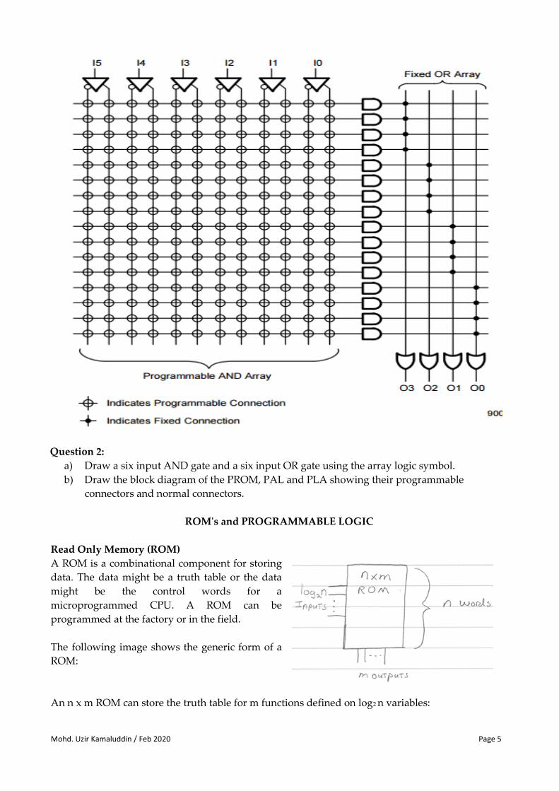
A portion of a logic diagram
A portion of a logic diagram is shown in figure below. The logic diagram shows all of the logic
resources available in a particular device. In each device, inputs are provided in true and
complement versions, as shown in the figure. These drive what are often called “input lines,” which
are the vertical lines in the logic diagram. These input lines can then be connected to product terms.
The name “product term” is really just a fancy name for an AND gate. However, PLDs provide
very wide gates, which can be cumbersome to draw. To save space, the product terms are drawn as
horizontal lines with a small AND gate symbol at one end to indicate the function being performed.
PAL Device Array structure
Mohd. Uzir Kamaluddin / Feb 2020 Page 5
Question 2:
a) Draw a six input AND gate and a six input OR gate using the array logic symbol.
b) Draw the block diagram of the PROM, PAL and PLA showing their programmable
connectors and normal connectors.
ROM's and PROGRAMMABLE LOGIC
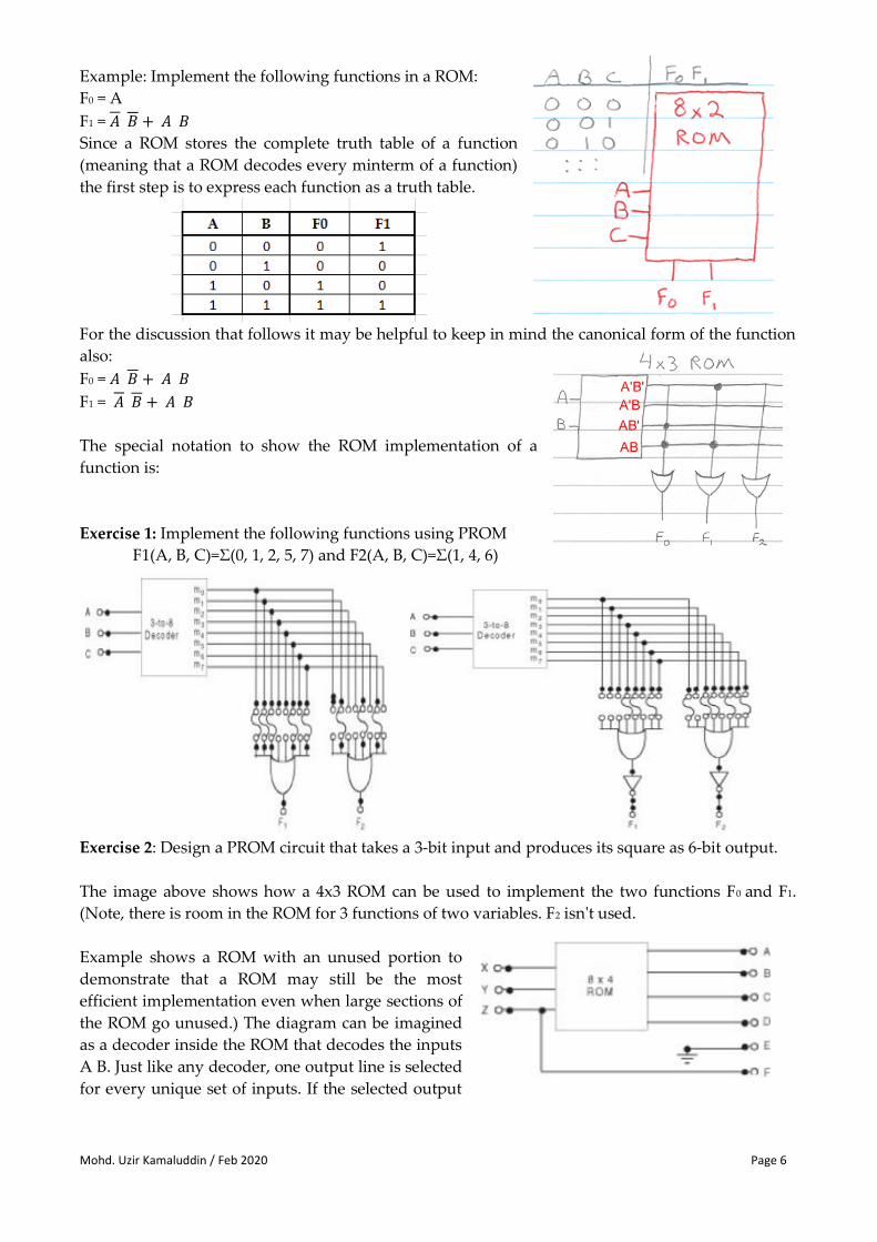
Read Only Memory (ROM)
A ROM is a combinational component for storing
data. The data might be a truth table or the data
might be the control words for a
microprogrammed CPU. A ROM can be
programmed at the factory or in the field.
The following image shows the generic form of a
ROM:
An n x m ROM can store the truth table for m functions defined on log2 n variables:
Mohd. Uzir Kamaluddin / Feb 2020 Page 6
Example: Implement the following functions in a ROM:
F0 = A
F1 =
Since a ROM stores the complete truth table of a function
(meaning that a ROM decodes every minterm of a function)
the first step is to express each function as a truth table.
For the discussion that follows it may be helpful to keep in mind the canonical form of the function
also:
F0 =
F1 =
The special notation to show the ROM implementation of a
function is:
Exercise 1: Implement the following functions using PROM
F1(A, B, C)=Σ(0, 1, 2, 5, 7) and F2(A, B, C)=Σ(1, 4, 6)
Exercise 2: Design a PROM circuit that takes a 3-bit input and produces its square as 6-bit output.
The image above shows how a 4x3 ROM can be used to implement the two functions F0 and F1.
(Note, there is room in the ROM for 3 functions of two variables. F2 isn't used.
Example shows a ROM with an unused portion to
demonstrate that a ROM may still be the most
efficient implementation even when large sections of
the ROM go unused.) The diagram can be imagined
as a decoder inside the ROM that decodes the inputs
A B. Just like any decoder, one output line is selected
for every unique set of inputs. If the selected output

Mohd. Uzir Kamaluddin / Feb 2020 Page 7
line is connected to an OR gate the function
associated with the OR gate will have a value of 1
for the particular set of inputs.
Note that the image above also shows a new way
to indicate multiple connections with a single
line.
For example:
A single vertical line that intersects 4 horizontal lines represents
potentially 4 different lines or connections. This is a notational
convenience when talking about ROM's, PLA's, and PAL's because it
makes the diagrams much easier to read.
The circles at the intersection of two lines indicates a connection.
Connections are either formed at the factory or in the field. If they
are formed in the field a special programmable ROM is used. One
type of programmable ROM is a ROM that has a fuse at every
connection. Fuses at connections not wanted are burned by running
high current through the fuse. What is left are the connections that define the data within the ROM.
Observations
Not very efficient implementation of sparse functions.
A ROM that implements two functions does not require twice the number of gates as a
ROM that implements one function. (The decoder is shared by every output function.)
Some extra points
ROMs programmed at the factory are called mask ROMS because during fabrication the circuit
patterns are determined by a mask. There are several different types of field programmable ROMS:
PROM (Programmable Read-Only Memory) - This is the type that was discussed above.
Connections are fused and burned in the field with a PROM programmer.
EPROM (Erasable Programmable Read-Only Memory) - This type of ROM can be re-written
by shining an ultraviolet light through a window on the IC.
EEPROM (Electrically Erasable Programmable Read-Only Memory) - Rather than ultraviolet
light an extra high voltage is used to re-write the contents of this type of ROM.
Flash Memory - Instead of requiring extra high voltages flash memory devices work with
regular device voltages.
Programmable Logic
A programmable logic device works like a ROM but is a
more efficient solution for implementing sparse output
functions. (Not all minterms are decoded.)
There are two types of programmable logic devices:
PLA (Programmable Logic Array)
PAL (Programmable Array Logic)
As suggested earlier that a ROM had a decoder inside it
and could be visualized as:
The image above also defines two terms that will be used to distinguish between PLA and PAL
devices:

Mohd. Uzir Kamaluddin / Feb 2020 Page 8
AND Array - this is the portion of the device that decodes the inputs. The AND array
determines the minterms decoded by the device. A ROM decodes all possible minterms.
OR Array - this is the portion of the device that combines the minterms for the definition of
a function.
PLA
A PLA is a programmable logic device with a programmable AND array and a programmable OR
array.
A PLA with n inputs has fewer than 2n AND gates (otherwise there would be no advantage over a
ROM implementation of the same size). A PLA only needs to have enough AND gates to decode as
many unique terms as there are in the functions it will implement.
Because of the control-ability of the AND array and there is a limit to the number of terms that can
be specified in the AND array, it may be more economical to simplify the function before
implementing it with a PLA. If simplification is done to the function and then intended to
implement with a PAL device, it should also be kept in mind that product terms can be shared
between functions. (Product sharing is when two functions share a product term decoded by the
AND array. For example, in the image below the product term AB is shared between F0 and F1.)
Example: Implement the functions F0 F1 we introduced above using a PLA with 2 inputs, 3 product
terms, and 2 outputs.
The un-programmed PLA from the manufacture looks like:
After programming for the two functions
F0 F1 the state of the PLA is:
Notice that it only need three AND gates because there
are only three unique minterms in the functions F0 and
F1. Also, notice that since that the OR array can be
controlled, it can share with the minterm AB in the
definitions of both functions.
Note, there may be an advantage to simplifying the
functions before implementing. In the example used here
there is no advantage. The simplified form of the
functions F0 and F1 still require 3 unique product terms. Because product terms can be shared
between functions it’s important to look for common product terms when simplifying.
Mohd. Uzir Kamaluddin / Feb 2020 Page 9
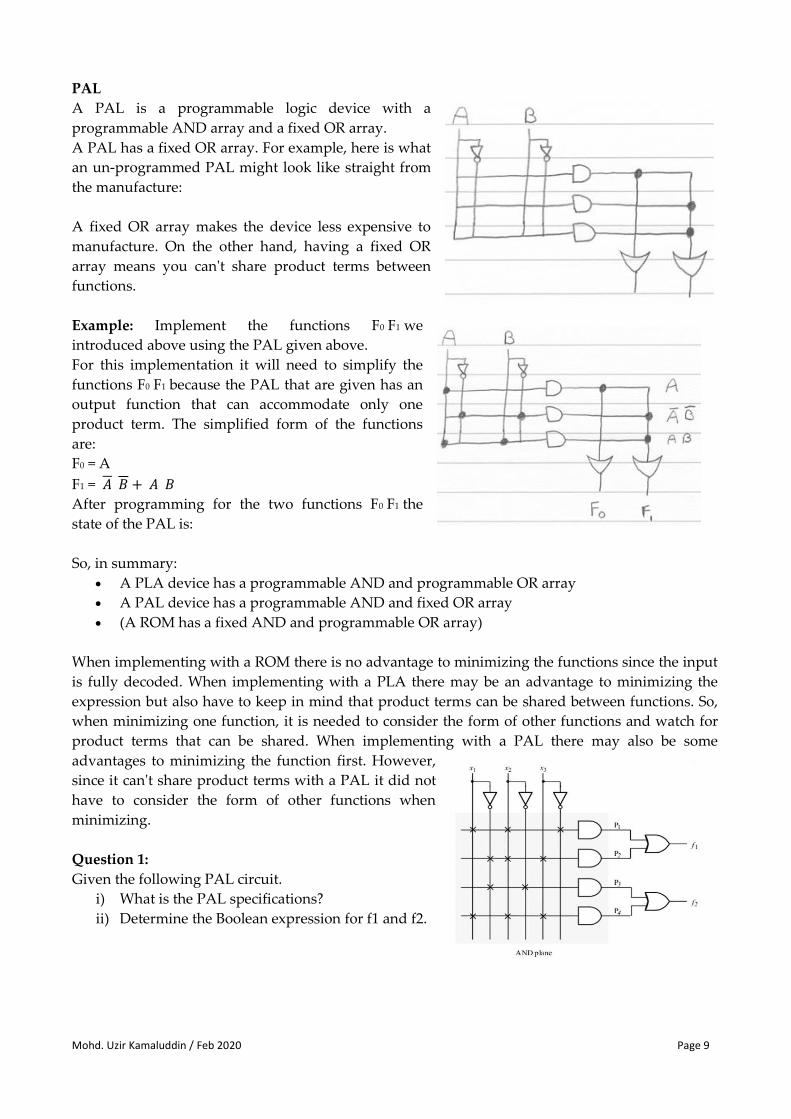
PAL
A PAL is a programmable logic device with a
programmable AND array and a fixed OR array.
A PAL has a fixed OR array. For example, here is what
an un-programmed PAL might look like straight from
the manufacture:
A fixed OR array makes the device less expensive to
manufacture. On the other hand, having a fixed OR
array means you can't share product terms between
functions.
Example: Implement the functions F0 F1 we
introduced above using the PAL given above.
For this implementation it will need to simplify the
functions F0 F1 because the PAL that are given has an
output function that can accommodate only one
product term. The simplified form of the functions
are:
F0 = A
F1 =
After programming for the two functions F0 F1 the
state of the PAL is:
So, in summary:
A PLA device has a programmable AND and programmable OR array
A PAL device has a programmable AND and fixed OR array
(A ROM has a fixed AND and programmable OR array)
When implementing with a ROM there is no advantage to minimizing the functions since the input
is fully decoded. When implementing with a PLA there may be an advantage to minimizing the
expression but also have to keep in mind that product terms can be shared between functions. So,
when minimizing one function, it is needed to consider the form of other functions and watch for
product terms that can be shared. When implementing with a PAL there may also be some
advantages to minimizing the function first. However,
since it can't share product terms with a PAL it did not
have to consider the form of other functions when
minimizing.
Question 1:
Given the following PAL circuit.
i) What is the PAL specifications?
ii) Determine the Boolean expression for f1 and f2.

Mohd. Uzir Kamaluddin / Feb 2020 Page 10
Question 2:
Given the following PAL circuit.
i) What is the PAL specifications?
ii) Determine the Boolean expressions for F1, F2,
F3 and F4.
Question 3:
A combinational circuit having the following truth table is implemented using (3 x 4 x 2) PLA
where A, B, C are inputs and F1, F2 are outputs.
A B C F1 F2
0 0 0 1 1
0 0 1 1 0
0 1 0 1 0
0 1 1 0 0
1 0 0 1 0
1 0 1 0 1
1 1 0 0 1
1 1 1 0 1
Show how the circuit is implemented.
Question 4:
Implement the following Boolean functions using (4 x 8 x 3) PAL device.
W(A, B, C) =
X(A, B, C) =
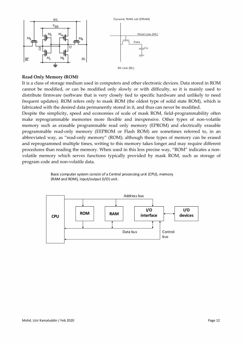
Memory
Memory refers to the physical devices used to store sequences of instructions or data on a
temporary or permanent basis for use in a computer or other digital electronic device. Primary
memory is used for the information in physical systems which function at high-speed (i.e. RAM), as
a distinction from secondary memory, which are physical devices for program and data storage
which are slow to access but offer higher memory capacity. Primary memory stored on secondary
memory is called virtual memory.
The term memory, meaning primary memory is often associated with addressable semiconductor
memory, i.e. integrated circuits consisting of silicon-based transistors, used for example as primary
memory but also other purposes in computers and other digital electronic devices. There are two

Mohd. Uzir Kamaluddin / Feb 2020 Page 11
main types of semiconductor memory: volatile and non-volatile. Examples of non-volatile memory
are flash memory and ROM/PROM/EPROM/EEPROM memory.
Example of volatile memory are primary memory (typically dynamic RAM, DRAM), and fast CPU
cache memory (typically static RAM, SRAM, which is fast but energy-consuming and offer lower
memory capacity per area unit than DRAM).
Most semiconductor memory is organized into memory cells or bi-stable flip-flops, each storing one
bit (0 or 1). Flash memory organization includes both one bit per memory cell and multiple bits per
cell (called MLC, Multiple Level Cell). The memory cells are grouped into words of fixed word
length, for example 1, 2, 4, 8, 16, 32, 64 or 128 bit. Each word can be accessed by a binary address of
N bit, making it possible to store 2N words in the memory. This implies that processor registers
normally are not considered as memory, since they only store one word and do not include an
addressing mechanism.
The term storage is often used to describe secondary memory such as tape, magnetic disks and
optical discs (CD-ROM and DVD-ROM).
Random Access Memory (RAM)
It is a form of computer data storage. A random-access device allows stored data to be accessed
directly in any random order. In contrast, other data storage media such as hard disks, CDs, DVDs
and magnetic tape, as well as early primary memory types such as drum memory, read and write
data only in a predetermined order, consecutively, because of mechanical design limitations.
Therefore the time to access a given data location varies significantly depending on its physical
location. Today, random-access memory takes the form of integrated circuits. Strictly speaking,
modern types of DRAM are not random access, as data is read in bursts, although the name
DRAM/RAM has stuck. However, many types of SRAM, ROM, OTP, and NOR flash are still
random access even in a strict sense. RAM is often associated with volatile types of memory (such
as DRAM memory modules), where its stored information is lost if the power is removed. Many
other types of non-volatile memory are RAM as well, including most types of ROM and a type of
flash memory called NOR-Flash.
The three main forms of modern RAM are static RAM (SRAM), dynamic RAM (DRAM) and phase-
change memory (PRAM). In SRAM, a bit of data is stored using the state of a flip-flop. This form of
RAM is more expensive to produce, but is generally faster and requires less power than DRAM
and, in modern computers, is often used as cache memory for the CPU. DRAM stores a bit
of data using a transistor and capacitor pair, which together comprise a memory cell. The capacitor
holds a high or low charge (1 or 0, respectively), and the transistor acts as a switch that lets the
control circuitry on the chip read the capacitor’s state of charge or change it. As this form of
memory is less expensive to produce than static RAM, it is the predominant form of computer
memory used in modern computers.
Both static and dynamic RAM is considered volatile, as their state is lost or reset when power is
removed from the system.
Mohd. Uzir Kamaluddin / Feb 2020 Page 12
Read Only Memory (ROM)
It is a class of storage medium used in computers and other electronic devices. Data stored in ROM
cannot be modified, or can be modified only slowly or with difficulty, so it is mainly used to
distribute firmware (software that is very closely tied to specific hardware and unlikely to need
frequent updates). ROM refers only to mask ROM (the oldest type of solid state ROM), which is
fabricated with the desired data permanently stored in it, and thus can never be modified.
Despite the simplicity, speed and economies of scale of mask ROM, field-programmability often
make reprogrammable memories more flexible and inexpensive. Other types of non-volatile
memory such as erasable programmable read only memory (EPROM) and electrically erasable
programmable read-only memory (EEPROM or Flash ROM) are sometimes referred to, in an
abbreviated way, as “read-only memory” (ROM); although these types of memory can be erased
and reprogrammed multiple times, writing to this memory takes longer and may require different
procedures than reading the memory. When used in this less precise way, “ROM” indicates a non-
volatile memory which serves functions typically provided by mask ROM, such as storage of
program code and non-volatile data.

Mohd. Uzir Kamaluddin / Feb 2020 Page 13
Programmable Read-Only Memory (PROM):
It can be written to or programmed via a special device called a PROM programmer. Typically, this
device uses high voltages to permanently destroy or create internal links (fuses or antifuses) within
the chip. Consequently, a PROM can only be programmed once.
Erasable Programmable Read-Only Memory (EPROM):
It can be erased by exposure to strong ultraviolet light (typically for 10 minutes or longer), then
rewritten with a process that again needs higher than usual voltage applied. Repeated exposure to
UV light will eventually wear out an EPROM, but the endurance of most EPROM chips exceeds
1000 cycles of erasing and reprogramming. EPROM chip packages can often be identified by the
prominent quartz “window” which allows UV light to enter. After programming, the window is
typically covered with a label to prevent accidental erasure. Some EPROM chips are factory-erased
before they are packaged, and include no window; these are effectively PROM.
Electrically Erasable Programmable Read-Only Memory (EEPROM):
It is based on a similar semiconductor structure to EPROM, but allows its entire contents (or
selected banks) to be electrically erased, then rewritten electrically, so that they need not be
removed from the computer (or camera, MP3 player, etc.). Writing or flashing an EEPROM is much
slower (milliseconds per bit) than reading from a ROM or writing to a RAM (nanoseconds in both
cases).
Electrically alterable read-only memory (EAROM) is a type of EEPROM that can be modified one
bit at a time. Writing is a very slow process and again needs higher voltage (usually around 12 V)
than is used for read access. EAROMs are intended for applications that require infrequent and
only partial rewriting. EAROM may be used as non-volatile storage for critical system setup
information; in many applications, EAROM has been supplanted by CMOS RAM supplied by
mains power and backed-up with a lithium battery.
Flash memory (or simply flash) can be erased and rewritten faster than ordinary EEPROM, and
newer designs feature very high endurance (exceeding 1,000,000 cycles). Modern NAND flash
makes efficient use of silicon chip area, resulting in individual ICs with a capacity as high as 32 GB
as of 2007; this feature, along with its endurance and physical durability, has allowed NAND flash
to replace magnetic in some applications (such as USB flash drives). Flash memory is sometimes
called flash ROM or flash EEPROM when used as a replacement for older ROM types, but not in
applications that take advantage of its ability to be modified quickly and frequently.

Mohd. Uzir Kamaluddin / Feb 2020 Page 14
Block diagram of Random Access Memory (RAM)
This block diagram introduces the main interface to the RAM chip.
The chip select input CS will enable or disable the RAM chip.
The address input lines will specify the address or location to read from or to write to.
The READ/ selects between reading from or writing to the memory chip.
The data in/out lines is where the data is coming in (for case of writing) or going out (for the case of
reading).
Block diagram of Read Only Memory (ROM)
This block diagram introduces the main interface to the ROM chip.
The chip select input CS’ will enable or disable the ROM chip.
The address input lines will specify the address or location to read from.
The data out lines is where the data is going out when there is reading operation.
Memory ICs
Shown here are the two commonly found memory ICs in the market.

Mohd. Uzir Kamaluddin / Feb 2020 Page 15
Exercise 1:
What is the meaning of the following terms related to memory and CPU:
a) Memory cell
b) Memory word
c) Capacity
d) Data Bus
e) Address Bus
f) Control Bus
g) R/ line
h) line
i) line
Exercise 2:
a) In a memory IC, what determines the size of the memory?
b) For the given memory size, determine the number of address lines:
i) 1K ii) 2K iii) 4K iv) 8K
c) For the given number of address lines, determine the memory size:
i) 10 ii) 11 iii) 12 iv) 13
Exercise 3:
If a memory IC is specified as (2K x 8), then determine:
a) Draw the block diagram of this memory IC.
b) The number of words that can be stored in this IC
c) The number of bits per word
d) The capacity of the memory IC
Exercise 4:
If a memory IC is specified as (64K x 8), then determine:
a) How many words can be stored on this IC?
b) How many data input and data output lines does it have?
c) How many memory cells does it contain?