Embed Size (px)
Citation preview

Coupling Extraction and Optimization for Heterogeneous2.5D Chiplet-Package Co-Design
MD Arafat KabirUniversity of Arkansas
Dusan PetranovicMentor Graphics
Yarui PengUniversity of Arkansas
AbstractIn recent years, 2.5D chiplet package designs have gained popular-ity in system integration of heterogeneous technologies. Currently,there exists no standard CAD flow that can design, analyze, andoptimize a complete heterogeneous 2.5D system. The traditionaldie-by-die design approach does not consider any package layersduring extraction and optimization, and an accurate chiplet-packageextraction can not be applied to heterogeneous designs without fun-damental changes in standard CAD tools. In this paper, we presentour Holistic and In-Context chiplet-package co-design flows forhigh-performance high-density 2.5D systems using standard ASICCAD tools with zero overhead on IO pipeline depth. Our flow en-compasses 2.5D-aware partitioning, chiplet-package co-planning,in-context extraction, iterative optimization, and post-design anal-ysis and verification of the entire 2.5D system. We design our pack-age planner with a routing and pin-planning strategy to minimizepackage routing congestion and timing overhead. An ARM Cortex-M0-based microcontroller system is designed as the benchmark.The performance gap to the reference 2D design reduces by 62.5%when chip-package interactions are taken into account in the holis-tic flow. Our in-context extraction achieves only 0.71% and 0.79%error on ground and coupling capacitance on a homogeneous sys-tem. Further, we implement a heterogeneous 2.5D system to demon-strate our novel in-context design and optimization methodology.
Keywords2.5D Design, Chiplet-Package Co-Optimization, Holistic, Hetero-geneous, In-Context.
1 IntroductionIn the post-Moore era, although transistor scaling and chip scal-ing are saturated, demands for increased functionality, performance,and bandwidth are still growing very fast. 2.5D integration technol-ogy is gaining popularity in increasing device density and perfor-mance at the system level. Moreover, it offers heterogenous inte-gration and hardware security applications [13, 14]. To support thisintegration scheme, the industry is developing compact and high-performance Wafer-Level-Packaging (WLP) solutions. As depictedin Fig. 1(a), in system integration schemes using Printed Circuit
Permission to make digital or hard copies of all or part of this work for personal orclassroom use is granted without fee provided that copies are not made or distributedfor profit or commercial advantage and that copies bear this notice and the full citationon the first page. Copyrights for components of this work owned by others than ACMmust be honored. Abstracting with credit is permitted. To copy otherwise, or republish,to post on servers or to redistribute to lists, requires prior specific permission and/or afee. Request permissions from [email protected] ’20, November 2–5, 2020, Virtual Event, USA© 2020 Association for Computing Machinery.ACM ISBN 978-1-4503-8026-3/20/11. . . $15.00https://doi.org/10.1145/3400302.3415718
Chip Chip
(a) PCB based integration scheme with ~250 µm pitch
Chip-Package gap = 30~50 µm
Chiplet Chiplet
(b) Flip-Chip integration scheme with ~20 µm pitch
Chip-Package gap = 1~5 µm
(c) High-density integration scheme with ~1 µm pitch (e.g., InFO)
Chiplet Chiplet
Figure 1: 2.5D integration schemes (a) PCB-based system, (b)flip-chip with an organic interposer, (c) high-density integrationscheme such as wafer-level-packaging
Boards (PCB) the packages become sufficiently large compared tothe chips. Moreover, the long interconnects between different partsof the system kill the system performance. The WLP integration so-lutions, as depicted in Fig. 1(b), (c) have chip-scale packages witha very fine pitch, and shorter interconnects, making them promis-ing candidates for high-performance system design. In the last fewyears, the industry has developed WLP technologies like eWLB [1],SWIFT [5], and InFO [12]. All these technologies are bringingchips and packages closer and closer in their every iteration.
In the current industry trend, all functional blocks of 2.5D sys-tems are designed independently in their own design environmentsand then mounted on package redistribution layers (RDL) as a com-plete system [6, 7]. Fig. 2(a) illustrates this traditional flow. Theanalysis and optimization of chiplets and the package are also con-ducted separately, without consideration of the interactions betweenthem. This traditional flow is sufficient when the gap between chipand package is large enough to make these interactions minimal.As shown in Fig. 1(b), this gap is around 30-50µm in the Flip-ChipWLP integration scheme. In such integration technologies, the tradi-tional flow works fine. However, with the development of advancedWLP processes like InFO, this gap is decreasing rapidly. Startingfrom the order of 10µm, this gap was reduced to 1.5µm [11] withina few years. With this trend, the chip-package gap will soon reduceto the sub-micron level, making the interactions between chip andpackage more prominent. As a result, to ensure system reliabilityand signal integrity, chip-package interactions must be consideredin timing and power analyses. In the current industry approach, it is

ICCAD ’20, November 2–5, 2020, Virtual Event, USA MD Arafat Kabir, Dusan Petranovic, and Yarui Peng
Complete 2.5D System Complete 2.5D System
Chip Design Tool
Package Design Tool
Design Information
Analysis
Design Assemble
Placement &
Routing
RDL
Routing
Package
Plan
Chiplet
Plan
Chiplet
Plan
Timing Budget Extraction and
Hierarchical Sub-Design Formation
Holistic Extraction
Chip-Package Floorplanning and
Package Wireload Estimation
Package
Parasitics
Final ChipletsFinal Package
(a) Traditional Flow (b) Proposed Flow
Final ChipletsFinal Package
Analysis
Placement &
Routing
Floorplanning
Partitioning
Gate Level Design
Chiplet
Design Flow
Chiplet
Footprints
RDL Routing
Package
Floorplanning
Analysis
Package
Design Flow
Gate Level Design
Partitioning
Figure 2: The traditional Die-by-Die design flow of a 2.5D sys-tem versus our proposed chiplet-package co-design flow withstandard CAD tools
not possible to accurately capture the interactions among the tightly-connected components of a 2.5D system. Standard design flow is indemand to fill in the missing pieces and address the new challengesof 2.5D system design.
In the die-by-die design approach, it is possible to achieve theshortest design time using off-the-shelf chiplets to implement a 2.5Dsystem. In this flow, chiplets and the package never actually inter-act with each other until after they are manufactured as a completesystem. As seen in Fig. 2(a), all steps of design and optimizationare performed independently in their own environments. However,to extract the best performance out of the system and to achievehigh system reliability optimizations and analysis in each designstep need to be performed in a holistic [10] way rather than con-sidering individual parts independently without taking into accountrest of the system.
Although the holistic design method is powerful and adaptive toany technologies, one fundamental issue is that it cannot be appliedto heterogeneous systems using standard ASIC tools. The hetero-geneity consists of multiple chiplets that are implemented in dif-ferent technologies. For example, AMD designed a processor corechiplet in 7nm with an IO chiplet in 14/12nm technology. For asmall design house, one challenge to implementing such designs isthe limitation of the CAD tools. In addition, some designs are intrin-sically very small in area and power budget, such as IoT devices.Having a large/high-performance IO system will create too muchoverhead for such system to be implemented with multiple chiplets.One solution is to allow highly-customized IO interface to be usedbetween chiplets which can be simplified into a few standard cells.However, as these cells are not designed for driving long RDL wireswith many technology variations, parasitics and STA analysis mustbe performed very carefully to avoid potential violations. To over-come these challenges, it is essential to design a CAD method forlow-cost IO systems that reduces timing and power overheads butstill captures all couplings between the chiplet and package to en-sure all design constraints are met.
In this paper, we propose a chiplet-package co-optimization flowthat incorporates the features required to achieve the design goalsin a high-density 2.5D integration technology. Fig. 2(b) shows theoverall steps of our flow. In this flow, we design 2.5D packagestogether with chiplets in the same design environment of the ex-isting commercial chip design tools. This enables the exchange ofnecessary design information between the chiplets and the pack-age during design and optimization steps. We also propose a novelin-context method to design heterogeneous systems using standardASIC CAD tools. Our flows use all standard libraries to design cus-tom pin drivers, achieve zero overhead on pipeline depth, and mini-mize the timing and power overhead.
Through the work presented in this paper, we claim the followingcontributions: (1) A unified tool flow that, for the first time, designsand optimizes chiplets and the package of high-density 2.5D sys-tems together taking into account the mutual interactions betweenthem; (2) A new holistic parasitic extraction and STA analysis flowfor homogeneous 2.5D systems with chiplets and the package con-sidered together; (3) A new in-context parasitic extraction and STAanalysis flow for heterogeneous 2.5D systems with chiplets-packageinteractions captured; (4) A comparative study between two 2.5Ddesigns to validate our Drop-in design approach and demonstratechiplet-package interaction impacts on two 2.5D systems Perfor-mance, Power, and Area (PPA).
To our best knowledge, there exists no other tool flow that im-plements holistic planning and optimizations of high-density 2.5Dsystems, including placement and routing of chiplets and the pack-ages together using commercial chip design tools.
2 CAD Flow and Reference DesignOur overall flow is demonstrated in Fig. 2(b). This flow is based ona previous work [4] that proposed a basic holistic design methodol-ogy for 2.5D systems. The first step of the flow is partitioning thesynthesized netlist into chiplets. The partitioning tool takes into ac-count the impacts of RDL and possible solution cases enabled by2.5D integration while exploring the partition solutions. After par-titioning, we perform the planning of chiplets and the package to-gether in the same design environment. The PDK is modified to in-clude the package layers along with the chiplet routing layers. Next,we generate an initial package routing and estimate the wire-loadsat the chiplet pins. Then, we split the overall design into individualchiplet and package sub-designs for parallel implementation. Afterthe co-planning and RDL routing, the chiplets and package can allbe implemented independently in their own design environments,with constraints propagated from the top level.
Individual chiplets are implemented following the traditional 2Dflow, using the top-level constraints and estimated package wire-loads. After the first iteration of placement and routing, the en-tire system is assembled for extraction. With this assembly, the ex-traction tool can capture the interactions among the routing layersacross chiplets and the package. Using the extracted parasitics, wecreate timing contexts for the chiplets and perform the second it-eration of chiplet design using these contexts. This ensures holis-tic optimization of the system and improves system performance ifpossible. Additional iterations can be carried out if there is scopeof more improvement. Finally, we assemble all the finished designsand perform extraction for analysis and sign-off verifications.

Coupling Extraction and Optimization for Heterogeneous 2.5D Chiplet-Package Co-Design ICCAD ’20, November 2–5, 2020, Virtual Event, USA
Core-Chiplet
1KB RAM
1KB RAM
1KB RAM
1KB RAM
1KB RAM
1KB RAM
1KB RAM
1KB RAM
Peripheral
Devices
1KB RAM
1KB RAM
1KB RAM
1KB RAM
1KB RAM
1KB RAM
1KB RAM
1KB RAM
GPIOGPIOCortex-M0
Processor
AHB Slave
Multiplexer
Memory
Interface
Memory Chiplet
Figure 3: System architecture and chiplet partitions of theCortex-M0-based reference design
For our case study, we design a micro-controller system based onARM Cortex-M0 core using our flow with Nangate45nm PDK. Thesystem consists of 16KB of memory and some peripheral devicescommonly found in a micro-controller system, like UART, timers,etc. The processor core is connected to an AHB bus, which acts asthe bridge to the rest of the system. The 16KB memory system hasfour 4KB banks. We further subdivide the 4KB banks into four 1KBmemory blocks. With such a granular design of the memory system,we have more options while performing partition and floorplan. Thesystem architecture and chiplet partitions of the micro-controllersystem are shown in Fig. 3. The core-chiplet contains all the logicblocks and 8KB memory while the mem-chiplet contains only therest 8KB of the memory. We use OpenRAM [2] memory compilerto compile the 1KB memory module with a one-byte word size.
Currently, standard chip design CAD tools do not support pack-age routing layers. To perform holistic planning and verification ofa 2.5D system, we need to load the chiplet and package designsin the same design environment. For this reason, we modify theNangate45nm technology to support both chiplets and the packagedesigns together in a chip design environment. We use M1-M7 forchiplet internal routing and adjust the top three layers, M8-M10, tomimic TSMC 2.5D InFO package routing layers. Table 1 and Fig. 4together describe our settings for the package layers.
3 Chiplet-Package Co-Planning and ModelingIn the traditional flow, floorplans of package and chiplets are pre-pared independently, without considering the interactions amongthem. If the package routing is not planned carefully, though eachchiplet might achieve very high performance, the entire system willperform poorly because of the timing bottlenecks through packagewires. At this step of our flow, we aim to plan the chiplet pin con-figuration and package floorplan in a holistic way to minimize thepackage-routing-related issues.
3.1 Package Floorplanning and RDL RoutingIn 2.5D systems, the RDL wires act as the timing bottlenecks, soperformance and signal integrity considerations play the main rolein RDL routing. Existing works [3, 8, 9] try to solve the routabil-ity between chiplet pins in the system. However, there are muchfewer RDL nets compared to intra-chip connections. As a result,routability and minimization of total wire-length are not the primaryconcerns. We develop an RDL planning tool that implements ourstrategy of chiplet-package floorplanning. It takes in chiplet netlists,technology, and timing information to generate package floorplan,RDL routing, and package wire-load estimations.
RDL1 (M8)
RDL2 (M9)
RDL3 (M10)
Cont. Pads (via7)
Figure 4: Package redistribution layer stack of our modifiedNangate45 PDK
Table 1: Parameters (in µm) of our modified Nangate45 PDKrouting layers
M6 via6 M7 via7 RDL1 viaR1 RDL2 viaR2 RDL3Height 2.28 3.08 3.9 7.5 12.5 17.5 22.5 27.5 32.5Thickness 0.8 0.82 3.6 5 5 5 5 5 5Width 0.4 0.4 2 5 10 10 10 10 10Spacing 0.4 0.44 2 10 10 20 10 20 10
In our strategy, we focus on developing a compact RDL routingplan with short and uniform wire-lengths to minimize routing is-sues like congestion, detours, and unequal bus wire delays betweenchiplets. We consider two chiplets at a time at the track assignmentstep. At first, we assign tracks to the pins of each chiplet separately.Then, a package floorplan is determined that connects all the tracksbetween the chiplets. Two pins of different chiplets assigned to thesame track are considered connected through the package wires.Fig. 5 shows the routing generated following our strategy. With theconnectivity defined, signal assignment of the chiplet pins are deter-mined using a greedy strategy based on net-slacks reported by thesynthesis tool.
3.2 Package Wireload EstimationAfter RDL routing, we calculate a rough estimation of packagewire-loads at the chiplet pins for the first iteration of chiplet im-plementation. For this estimation, package wire-load is calculatedas a linear function of the wire-length. This estimation is used toinform the chiplet implementation tool about the loads at the out-put of the driving cells of the pins. Being aware of the output load,during the optimization steps, it can make necessary adjustmentslike buffer insertion, cell resizing at the output nets. After the firstiteration of chiplet implementation, we extract the parasitics fromthe assembled design and use it to complete the second iterationof chiplet implementation. Subsequent iterations can be performeduntil design timing results converge. However, if the first estimateis good enough, the second iteration should be sufficient to meet apractical performance goal.
4 Chiplet-Package Co-Design and OptimizationThe physical design of individual chiplets and the package can beperformed using any commercial chip design environment that sup-ports hierarchical design flow. With the modified version of Nan-gate45nm technology, we load the entire system, chiplets and thepackage together, into the design environment. The chiplets are de-fined as modules in the partitioned netlist. We perform the place-ment and pin assignment of each module (chiplet) and packagerouting using scripts generated by our RDL planner tool. Then, weextract the timing budgets of chiplets and the package. After thisstep, the modules are separated as hierarchical sub-designs, and thepackage design is saved as the top-level design.

ICCAD ’20, November 2–5, 2020, Virtual Event, USA MD Arafat Kabir, Dusan Petranovic, and Yarui Peng
RDL3
RDL2RDL1
Figure 5: Inter-chiplet routing generated in our strategy. SomeRDL2 and RDL3 routes are hidden to show other layers.
4.1 Chiplet ImplementationDuring implementation, each chiplet is treated as a single 2D chipand designed using traditional chip design techniques. We modifythe chiplet design constraint files to include the wire-loads at thechiplet pins estimated by our RDL planner tool. We already havethe pin placement and the initial floorplan prepared at the top level.However, this floorplan can be adjusted if necessary as long as pinconfigurations are unchanged. After the floorplan is finalized, thepower distribution network is designed to ensure uniform power de-livery to all the parts of the chiplet. Then, we use standard toolsto perform the standard cell placement, power routing, clock net-work design, routing, and timing optimization. Lastly, filler cellsand metal fills are added to finish the chiplet design. Fig. 6(a) showsthe core-chiplet, which contains all the logic blocks and 8KB mem-ory. Fig. 6(b) shows the extended memory chiplet, which containsthe other 8KB memory.
4.2 Package ImplementationWith the timing budget and RDL plans generated by the RDL plan-ner tool, package designing can be finished in parallel alongside thechiplet implementations. However, more accurate and reliable op-timizations can be performed on the package design if we use thechiplets interface timing models extracted after their implementa-tions are complete. Because of the differences in the package andchip routing techniques, chip routing tools do not produce goodrouting for the package routing layers. Based on the strategy ex-plained in Section 3, our RDL planner generates routing scripts forpackage routing. We utilize these scripts to perform the routing be-tween the chiplets. After inter-chiplet routing is finished, we manu-ally route the rest of the I/O pins of the core-chiplet to the packageI/O pads. Fig. 7(b),(c) show the package routing of the two versionsof the example 2.5D system designed using the Drop-in method.The package wires connecting the two chiplets in Fig. 7(c) resem-ble the routing generated by the RDL planner tool.
4.3 Holistic ExtractionWith implemented chiplets and the package layouts, they are readyto be assembled in the integrated design environment again. Weload the modified version of Nangate45nm PDK in the chip design
tool and assemble the chiplets on the top-level design (package de-sign) using the partitions assemble commands of the tool. Thoughthis is a common step in the traditional 2D chip design flow, in2.5D systems, it is the step to harness some important benefits ofthis integration technology. Various interesting design techniqueslike plug-and-play [6], Drop-in design can be adopted at this step.
Using the Drop-in approach, we design two 2.5D systems withthe chiplets. Fig. 7(b) and (c) resemble these two systems. As bothchiplets and the package are together in the same environment, itis possible to accurately capture the interactions among them. Thiscreates a scope to perform some incremental optimizations of eachpart of the system to further improve the overall system perfor-mance and reliability. Fig. 7(d) is a zoomed-in view of the assem-bled system that clearly shows wires from the chiplet and packagealtogether. The wide horizontal wire marked RDL3 is a packagewire connecting pins of the two chiplets. The vertical wire markedM6 is a part of the power ring within the core-chiplet. The horizon-tal wires marked M1 are core-chiplet wires that connect the powerand ground rails of the standard cell rows to the power/ground ringon M6.
4.4 Iterative OptimizationsAfter design assembly and extraction, we run analysis to verify sys-tem performance. In this first iteration, as the package wire-loadsare just rough estimates, we almost always expect some room forimprovement. After the first iteration of design assembly, the extrac-tion tool can provide accurate parasitic information, and the analy-sis tool can generate a tighter timing budget. In the following itera-tions, instead of using the estimated wire-loads and timing budgets,we use the timing contexts extracted after design assemble of pre-vious iteration. With the new implementation of the chiplets, wecan perform another round of design-assemble and analysis. Therecan be multiple iterations of this process, each time with more ac-curate parasitics and timing budget until it is no longer possible toimprove system performance or the target performance is met. How-ever, with a good estimation generated by our RDL planner, only asecond iteration would be enough to verify and close the discrepan-cies. To justify this argument, in the next section, we present threedesign cases with no estimate, a rough estimate, and a near-accurateestimation of parasitics and timing budget.
5 Holistic Design for Homogeneous Systems5.1 Design VariationsTo study the impact of our flow on 2.5D system design, we prepareseveral design cases as presented here. In the results section, we per-form a comparative study among these design cases. Table 3 showsthe design parameters of these designs.5.1.1 Case-1: Reference 2D Design Fig. 7(a) shows the fin-ished 2D chip design. For this 2D implementation, we use the syn-thesized netlist prepared before the partition stage. The die area isa square with a side length of 550µm. Though the standard cellsoccupy approximately 10% of the area, this floorplan allows themto spread out in all directions to some extent. We perform the de-sign steps like standard cell placement, clock tree synthesis, andtime design, routing, and post-routing optimizations using the toolsintegrated with the chip design environment.

Coupling Extraction and Optimization for Heterogeneous 2.5D Chiplet-Package Co-Design ICCAD ’20, November 2–5, 2020, Virtual Event, USA
(a) Core System Chiplet (b) Extended Memory Chiplet
Figure 6: Layouts of the chiplets for 2.5D integration
5.1.2 Case-2: 2.5D Designs The first 2.5D design (Case-2A)is a Context-Free Single-Pass 2.5D design. In this design, the RDLplanner tool does not estimate the impact of package wires. Fig. 6shows the finished chiplets prepared in the Case-2A design. 2.5D in-tegration enables several flexible design approaches like plug-and-play, Drop-in method. Based on Case-2A design, we implement twosystems (Case-2B) using the Drop-in design approach at the designassemble stage. In one design, we have just the core-chiplet in thepackage, which is a fully-functional system with only 8KB of mem-ory. Fig. 7(b) shows this core-chiplet only system. In the other de-sign, we include both chiplets in the package where the completesystem has 16KB memory. Fig. 7(c) resembles this extended mem-ory system. Table 4 presents a comparative study of these two Drop-in systems.5.1.3 Case-3: Context-Aware Optimized 2.5D Designs Inthis design, we try to include chip-package interactions in the de-sign and optimization steps as much as possible. Unlike the tradi-tional flow, we perform iterative improvement to achieve the max-imum achievable performance out of the 2.5D system. We use theRDL planner tool to generate top-level floorplans, package routing,greedy signal assignment, and estimated wire-loads. After hierar-chical sub-design formation, we use the estimated wire-loads to im-plement the chiplets in the first iteration. After the second iteration,we performed more iterations. As there was no additional improve-ment in system performance, we take the second iteration output asthe final design for this design case.
5.2 Holistic Extraction and Analysis ResultsTraditional industry-standard flow uses FEM tools to perform pack-age extraction with S-parameters to determine package power andsignal integrity. Unlike the traditional flow, the entire 2.5D systemis in the same design environment after design assembly. Using thisholistic extraction result, our flow can achieve more accurate andreliable analysis results. The extraction results of Design Case-3 fi-nal iteration are presented in Table 2. For readability, we lumpedthe coupling capacitances among layers M1-M5.
As observed from the extraction result, there exists sufficient cou-pling between RDL1 of package and M6 of chiplets. Though the toprouting layer of the chiplets is M7, as seen in Table 3, the total wire-length on M7 is very small compared to that on M6. That is whythe RDL1 coupling capacitance value with M6 is greater than thatwith M7. Such detailed interaction between chiplet and package canonly be captured through a holistic extraction process as presentedin our flow. This chip-package coupling, along with the delay intro-duced by the package wires, greatly affects the system performance.Shown in Table 3, our analysis flow reveals this performance degra-dation. After all the possible traditional chip-level optimizations of
(b) Case-2B: 2.5D Core-only
RDL3
M6
M1
(d) Zoom-in Shot(c) Case-3: 2.5D with 16KB
(a) Case-1: 2D Chip
Figure 7: Design layouts of (a) monolithic 2D reference design,(b) assembled Core-only system, (c) assembled 2.5D system withextended memory, and (d) zoom-in shot.
Table 2: Coupling and ground capacitances (in fF) betweenrouting layers of design Case-3 final iteration
M1-M5 M6 M7 RDL1 RDL2 RDL3M1-M5 6120 442.2 28.65 52.95 8.102 5.862
M6 442.2 596.6 78.03 122.8 12.98 10.53M7 28.65 78.03 30.63 15.02 1.509 2.256
RDL1 52.95 122.8 15.02 299.3 1016 39.06RDL2 8.102 12.98 1.509 1015 298.3 1085RDL3 5.862 10.53 2.256 39.06 1084 578.4
Ground CapacitanceMetal Layer M1-M5 M6 M7 RDL1 RDL2 RDL3Capacitance 21119 2054 272 1040 247 636
Design Case-2, the best system performance we achieve is 245MHz.This is significantly slower than the performance of the reference2D system, which is 333MHz. In Design Case-3, we apply our ownstrategies to minimize this degradation.
The estimated package wire-loads used in the first iteration ofchiplet design are calculated purely as a linear function of pack-age wire-length and do not consider the coupling. Because of thissimplified wire-load model, on average, the wire-loads are under-estimated by the RDL planner tool. However, even with this crudeestimation, we can achieve a good performance improvement overthe Case-2 Design. As observed from Table 3, after the first iterationof Case-3 Design, which uses this estimated wire-load, we achievea system frequency of 280MHz, which is approximately 40% reduc-tion in the performance gap between the reference 2D design andthe Case-2 Design. This result reveals the significance of the holis-tic consideration of chiplet-package interactions, even at the earlydesign steps of 2.5D systems.

ICCAD ’20, November 2–5, 2020, Virtual Event, USA MD Arafat Kabir, Dusan Petranovic, and Yarui Peng
Table 3: Comparison of die/chiplet analysis results of design cases with both chiplets
Design Case Case-1 Case-2 Case-3 first iteration Case-3 2nd/final iterationChip Design 2D Chip Core Chiplet Mem. Chiplet Core Chiplet Mem. Chiplet Core Chiplet Mem. ChipletLogic Gates# 17595 17783 132 17915 148 18214 45Buffer/Inverter# 3700 2740 132 2865 148 2955 45Die Size (µm×µm) 550×550 390×590 350×470 390×590 350×470 390×590 350×470Total Chip Wirelength (mm) 412.9 350.9 40.14 361.2 45.07 366.3 41.99M6 Wirelength (mm) 79.94 30.81 5.986 31.86 8.201 31.42 8.445M7 Wirelength (mm) 0 1.783 0.598 1.875 0.589 2.02 0.624Max Frequency (MHz) 333 245 280 300Performance Gap 0% 100% 60.23% 37.50%Chip Power (mW) 10.6 7.751 0.194 9.043 0.216 9.840 0.162
Table 4: Comparison between Drop-in systems
System Design Core Only Full System OptimizedTotal Memory 8KB 16KB 16KBChip-Package Cap 120.7864fF 217.4089fF 232fFMax Frequency 300MHz 245MHz 300MHzSystem Power 9.578mW 8.26mW 10.0mWPakacage wirelength 35.41mm 94.027mm 94.027mmPackage Size 1.3mm x 1.15mm
5.3 Iterative Optimization ResultsIn the second iteration of Case-3 Design, we use the extracted par-asitics from the assembled design of the first iteration. This itera-tion adjusts the chiplet designs to match the actual capacitive loadson driving cells. The adjustments in the second iteration can beobserved from the buffer counts of the chiplets in Table 3. Com-pared to the first iteration design, the total buffer count of the core-chiplet is increased. However, the total buffer count of memory-chiplet is significantly decreased in the second iteration. This isbecause, though the buffers driving the previously under-estimatedwire-loads are up-sized by two to four times, the smaller buffersdriving the over-estimated wire-loads are completely removed. Allthese adjustments are performed by the traditional chip design toolswithout applying any special settings. Moreover, the system perfor-mance further improved to 300MHz, which is very close to our ref-erence 2D design case.
Comparisons between these designs clearly show that it is essen-tial to consider the chip-package interactions holistically to obtainthe best performance out of a 2.5D system. Our flow aims at achiev-ing this holistic co-design and optimization goal starting at the earlyplanning stage of the design. Shown in Table 3, with minimal chip-package interaction consideration, the performance gap between thereference 2D system and Case-2 2.5D system is 88MHz. Even withan early estimation in the first iteration, we close this performancegap in the first iteration of Case-3 Design by around 40%. Finally,with the iterative approach, we close this gap by 62.5% in the sec-ond iteration.
5.4 Comparative Study of Drop-in DesignsTable 4 shows the comparison between two 2.5D systems designedusing the Drop-in approach. The Chip-Package coupling capaci-tance is larger for the memory extended full system because of morepackage wires, as seen in Fig. 7(b),(c). The critical timing path forthe extended system is between the core and memory chiplets. As
Table 5: Comparison of Holistic (Holi) vs In-Context (In-C)ground (GCAP) and coupling (CCAP) capacitance extractionresults (in fF) of Case-3 final homogeneous design.
Metal Layer M1-M5 M6 M7 R1 R2 R3In-C GCAP 21119 2053 273 1103 306 696Holi GCAP 21119 2054 272 1040 247 636
In-C GCAP Err 0.00% -0.01% 0.09% 6.03% 24.0% 9.46%In-C CCAP 9171 1265 153 1563 2489 1765Holi CCAP 9172 1263 156 1544 2421 1721
In-C CCAP Err -0.01% 0.17% -2.10% 1.20% 2.81% 2.56%
a result, in the absence of the extra memory chiplet, the system canoperate at a higher system frequency. As Table 4 shows, the Core-Only system can run at 300MHz while the full system without opti-mizations runs at 245MHz. The Core-Only system can be a low-cost, high-performance solution for the applications where 8KBmemory is sufficient. On the other hand, the memory extended sys-tem is suitable for memory-intensive applications. Between thesetwo implementations of the system, the only change needed is inthe package level design, which is much cheaper and easier thanmaking changes in the chip level designs. This approach offers ap-plication engineers the opportunity to make tradeoffs between cost,performance, and memory while selecting his implementation sys-tem. Designers can utilize our holistic flow to take full advantageof this design approach and implement several flavors of a 2.5Dsystem per application needs.
6 In-Context Design for Heterogeneous SystemsSince the holistic flow requires to assemble the chiplets into a uni-fied design environment, it cannot be applied to heterogeneous sys-tems where the device stack are different. At the present, no stan-dard CAD flows support including two different technology filesinto a single physical design tools. Therefore, we present our in-context design method which allows an arbitrary number of chipletsin different technologies integrated with chiplet-package couplingconsidered altogether. It is completely compatible with all standardASIC tools for design, extraction, and analysis.
6.1 In-Context Design and Validation ResultsThe first step is to create in-context designs as another level of de-sign hierarchy. The context of a chiplet should include the area cov-ering the whole chiplet and necessary neighboring regions. Thisensures all chiplet-package interactions are considered during the
Coupling Extraction and Optimization for Heterogeneous 2.5D Chiplet-Package Co-Design ICCAD ’20, November 2–5, 2020, Virtual Event, USA
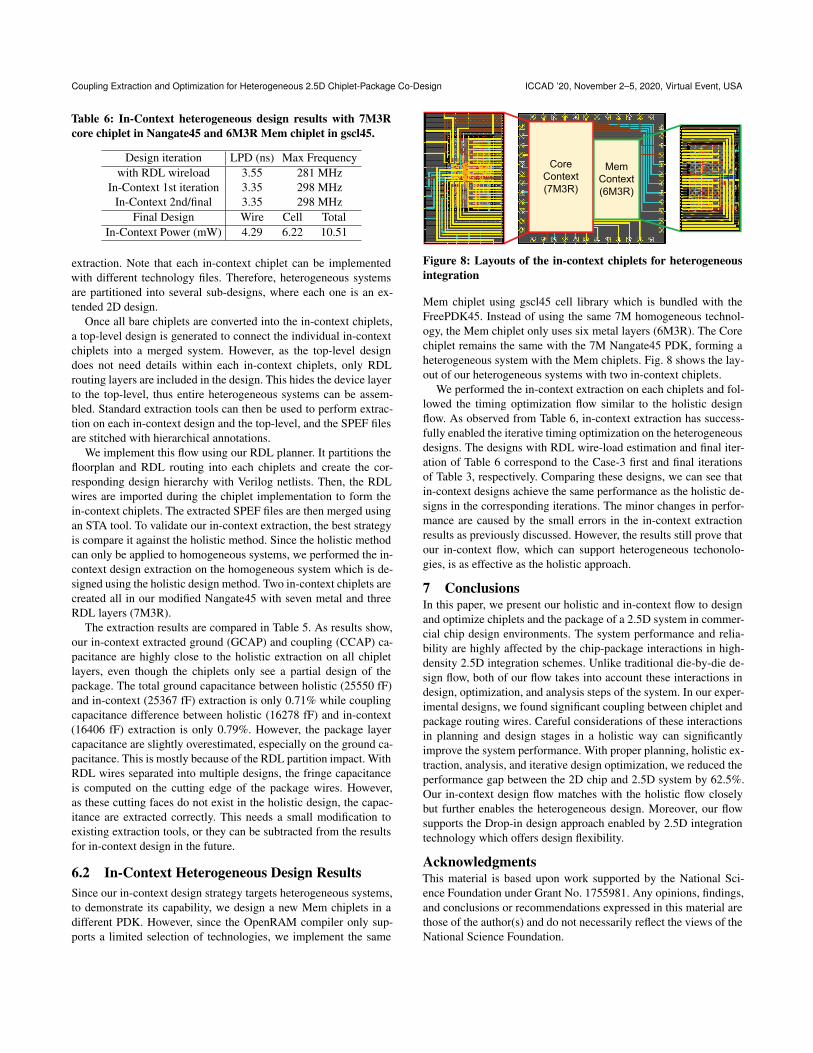
Table 6: In-Context heterogeneous design results with 7M3Rcore chiplet in Nangate45 and 6M3R Mem chiplet in gscl45.
Design iteration LPD (ns) Max Frequencywith RDL wireload 3.55 281 MHz
In-Context 1st iteration 3.35 298 MHzIn-Context 2nd/final 3.35 298 MHz
Final Design Wire Cell TotalIn-Context Power (mW) 4.29 6.22 10.51
extraction. Note that each in-context chiplet can be implementedwith different technology files. Therefore, heterogeneous systemsare partitioned into several sub-designs, where each one is an ex-tended 2D design.
Once all bare chiplets are converted into the in-context chiplets,a top-level design is generated to connect the individual in-contextchiplets into a merged system. However, as the top-level designdoes not need details within each in-context chiplets, only RDLrouting layers are included in the design. This hides the device layerto the top-level, thus entire heterogeneous systems can be assem-bled. Standard extraction tools can then be used to perform extrac-tion on each in-context design and the top-level, and the SPEF filesare stitched with hierarchical annotations.
We implement this flow using our RDL planner. It partitions thefloorplan and RDL routing into each chiplets and create the cor-responding design hierarchy with Verilog netlists. Then, the RDLwires are imported during the chiplet implementation to form thein-context chiplets. The extracted SPEF files are then merged usingan STA tool. To validate our in-context extraction, the best strategyis compare it against the holistic method. Since the holistic methodcan only be applied to homogeneous systems, we performed the in-context design extraction on the homogeneous system which is de-signed using the holistic design method. Two in-context chiplets arecreated all in our modified Nangate45 with seven metal and threeRDL layers (7M3R).
The extraction results are compared in Table 5. As results show,our in-context extracted ground (GCAP) and coupling (CCAP) ca-pacitance are highly close to the holistic extraction on all chipletlayers, even though the chiplets only see a partial design of thepackage. The total ground capacitance between holistic (25550 fF)and in-context (25367 fF) extraction is only 0.71% while couplingcapacitance difference between holistic (16278 fF) and in-context(16406 fF) extraction is only 0.79%. However, the package layercapacitance are slightly overestimated, especially on the ground ca-pacitance. This is mostly because of the RDL partition impact. WithRDL wires separated into multiple designs, the fringe capacitanceis computed on the cutting edge of the package wires. However,as these cutting faces do not exist in the holistic design, the capac-itance are extracted correctly. This needs a small modification toexisting extraction tools, or they can be subtracted from the resultsfor in-context design in the future.
6.2 In-Context Heterogeneous Design ResultsSince our in-context design strategy targets heterogeneous systems,to demonstrate its capability, we design a new Mem chiplets in adifferent PDK. However, since the OpenRAM compiler only sup-ports a limited selection of technologies, we implement the same
Core
Context
(7M3R)
Mem
Context
(6M3R)
Figure 8: Layouts of the in-context chiplets for heterogeneousintegration
Mem chiplet using gscl45 cell library which is bundled with theFreePDK45. Instead of using the same 7M homogeneous technol-ogy, the Mem chiplet only uses six metal layers (6M3R). The Corechiplet remains the same with the 7M Nangate45 PDK, forming aheterogeneous system with the Mem chiplets. Fig. 8 shows the lay-out of our heterogeneous systems with two in-context chiplets.
We performed the in-context extraction on each chiplets and fol-lowed the timing optimization flow similar to the holistic designflow. As observed from Table 6, in-context extraction has success-fully enabled the iterative timing optimization on the heterogeneousdesigns. The designs with RDL wire-load estimation and final iter-ation of Table 6 correspond to the Case-3 first and final iterationsof Table 3, respectively. Comparing these designs, we can see thatin-context designs achieve the same performance as the holistic de-signs in the corresponding iterations. The minor changes in perfor-mance are caused by the small errors in the in-context extractionresults as previously discussed. However, the results still prove thatour in-context flow, which can support heterogeneous techonolo-gies, is as effective as the holistic approach.
7 ConclusionsIn this paper, we present our holistic and in-context flow to designand optimize chiplets and the package of a 2.5D system in commer-cial chip design environments. The system performance and relia-bility are highly affected by the chip-package interactions in high-density 2.5D integration schemes. Unlike traditional die-by-die de-sign flow, both of our flow takes into account these interactions indesign, optimization, and analysis steps of the system. In our exper-imental designs, we found significant coupling between chiplet andpackage routing wires. Careful considerations of these interactionsin planning and design stages in a holistic way can significantlyimprove the system performance. With proper planning, holistic ex-traction, analysis, and iterative design optimization, we reduced theperformance gap between the 2D chip and 2.5D system by 62.5%.Our in-context design flow matches with the holistic flow closelybut further enables the heterogeneous design. Moreover, our flowsupports the Drop-in design approach enabled by 2.5D integrationtechnology which offers design flexibility.
AcknowledgmentsThis material is based upon work supported by the National Sci-ence Foundation under Grant No. 1755981. Any opinions, findings,and conclusions or recommendations expressed in this material arethose of the author(s) and do not necessarily reflect the views of theNational Science Foundation.

ICCAD ’20, November 2–5, 2020, Virtual Event, USA MD Arafat Kabir, Dusan Petranovic, and Yarui Peng
References[1] M. Brunnbauer, T. Meyer, G. Ofner, K. Mueller, and R. Hagen. 2008. Embedded
Wafer Level Ball Grid Array (eWLB). In International Electronics Manufactur-ing Technology Conference. 1–6. https://doi.org/10.1109/IEMT.2008.5507866
[2] Matthew R. Guthaus, James E. Stine, Samira Ataei, Brian Chen, Bin Wu,and Mehedi Sarwar. 2016. OpenRAM: An Open-source Memory Com-piler. In International Conference on Computer-Aided Design. 93:1–93:6.https://doi.org/10.1145/2966986.2980098
[3] Jia-Wei Fang and Yao-Wen Chang. 2008. Area-I/O flip-chip routing for chip-package co-design. In International Conference on Computer-Aided Design. 518–522. https://doi.org/10.1109/ICCAD.2008.4681624
[4] MD Arafat Kabir and Yarui Peng. 2020. Chiplet-Package Co-Design For 2.5D Systems Using Standard ASIC CAD Tools. InAsia and South Pacific Design Automation Conference. 351–356.https://doi.org/10.1109/ASP-DAC47756.2020.9045734
[5] W. Ki, W. Lee, I. MoK, I. Lee, W. Do, M. Kolbehdari, A. Copia, S. Jayaraman,C. Zwenger, and K. Lee. 2018. Chip Stackable, Ultra-thin, High-Flexibility3D FOWLP (3D SWIFT® Technology) for Hetero-Integrated Advanced 3DWL-SiP. In IEEE Electronic Components and Technology Conference. 580–586.https://doi.org/10.1109/ECTC.2018.00092
[6] Jinwoo Kim, Gauthaman Murali, Heechun Park, Eric Qin, Hyoukjun Kwon,Venkata Chaitanya, Krishna Chekuri, Nihar Dasari, Arvind Singh, Minah Lee,Hakki Mert Torun, Kallol Roy, Madhavan Swaminathan, Saibal Mukhopadhyay,Tushar Krishna, and Sung Kyu Lim. 2019. Architecture, Chip, and Package Co-design Flow for 2.5D IC Design Enabling Heterogeneous IP Reuse. In Design Au-tomation Conference. 178:1–178:6. https://doi.org/10.1145/3316781.3317775
[7] W. Liu, Min-Sheng Chang, and T. Wang. 2014. Floorplanning and signal assign-ment for silicon interposer-based 3D ICs. In Design Automation Conference. 1–6.https://doi.org/10.1145/2593069.2593142
[8] J. Minz and S. K. Lim. 2006. Block-level 3-D Global Routing Withan Application to 3-D Packaging. IEEE Transactions on Computer-AidedDesign of Integrated Circuits and Systems 25, 10 (Oct 2006), 2248–2257.https://doi.org/10.1109/TCAD.2005.860952
[9] J. R. Minz and Sung Kyu Lim. 2004. A global router for system-on-package tar-geting layer and crosstalk minimization. In Electrical Performance of ElectronicPackaging. 99–102. https://doi.org/10.1109/EPEP.2004.1407557
[10] Y. Peng, T. Song, D. Petranovic, and S. K. Lim. 2017. Parasitic Extraction forHeterogeneous Face-to-Face Bonded 3-D ICs. IEEE Transactions on Compo-nents and Packaging and Manufacturing Technology 7, 6 (June 2017), 912–924.https://doi.org/10.1109/TCPMT.2017.2677963
[11] H. Pu, H. J. Kuo, C. S. Liu, and D. C. H. Yu. 2018. A Novel Submi-cron Polymer Re-Distribution Layer Technology for Advanced InFO Pack-aging. In IEEE Electronic Components and Technology Conference. 45–51.https://doi.org/10.1109/ECTC.2018.00015
[12] C. Tseng, C. Liu, C. Wu, and D. Yu. 2016. InFO (Wafer Level Integrated Fan-Out) Technology. In IEEE Electronic Components and Technology Conference.1–6. https://doi.org/10.1109/ECTC.2016.65
[13] Y. Xie, C. Bao, Y. Liu, and A. Srivastava. 2016. 2.5D/3D Integration Technolo-gies for Circuit Obfuscation. In International Workshop on Microprocessor andSOC Test and Verification. 39–44. https://doi.org/10.1109/MTV.2016.17
[14] Y. Xie, C. Bao, and A. Srivastava. 2017. Security-Aware 2.5D Integrated CircuitDesign Flow Against Hardware IP Piracy. Computer 50, 5 (May 2017), 62–71.https://doi.org/10.1109/MC.2017.121