Embed Size (px)
Citation preview
COUPLED SURFACE PLASMON STRUCTURES AND
APPLICATIONS
a thesis
submitted to the department of materials science and
nanotechnology
and the institute of engineering and sciences
of bilkent university
in partial fulfillment of the requirements
for the degree of
master of science
By
Kemal Gurel
September 2009
I certify that I have read this thesis and that in my opinion it is fully adequate,
in scope and in quality, as a thesis for the degree of Master of Science.
Assist. Prof. Dr. Mehmet Bayındır (Supervisor)
I certify that I have read this thesis and that in my opinion it is fully adequate,
in scope and in quality, as a thesis for the degree of Master of Science.
Res. Assist. Prof. Dr. Aykutlu Dana (Co-Supervisor)
I certify that I have read this thesis and that in my opinion it is fully adequate,
in scope and in quality, as a thesis for the degree of Master of Science.
Assoc. Prof. Dr. Mehmet Ozgur Oktel
I certify that I have read this thesis and that in my opinion it is fully adequate,
in scope and in quality, as a thesis for the degree of Master of Science.
Assist. Prof. Dr. Ali Kemal Okyay
Approved for the Institute of Engineering and Sciences:
Prof. Dr. Mehmet BarayDirector of Institute of Engineering and Sciences
ii

ABSTRACT
COUPLED SURFACE PLASMON STRUCTURES AND
APPLICATIONS
Kemal Gurel
M.S. in Materials Science and Nanotechnology
Supervisor: Assist. Prof. Dr. Mehmet Bayındır
September 2009
Surface plasmons have attracted great interest during past decades due to their
unique physical properties. In this thesis, we study grating-coupled surface plas-
mons for sensing and filtering applications. We first present simple physical
and chemical procedures that allow tuning and modification of the topography
of gratings present in optical storage discs into geometries optimal for grating
coupled plasmon resonance excitation. After proper metal coating, the tuned
surfaces exhibit sharp plasmon resonances that can be excited at wavelengths
ranging from 260 nm to over 2.7 µm with relatively high quality factors. As
an immediate exemplary application, use of such optimized gratings in aqueous
medium for refractive index measurement is demonstrated.
We also report another plasmonic component based on a pair of surfaces dis-
playing grating coupled plasmon enhanced transmission. We observe high quality
factor transmission peaks as high as 100 through our plasmonic filter based on
gratings obtained directly from optical storage disks. Wavelength and polar-
ization dependent transmission is also demonstrated in the visible and infrared
portions of the spectrum. The resonance wavelength of this filter can be tuned
by simply changing the angle of incidence. Numerical calculations agree well
iii

with measurements. Our work can open up directions toward disposable optical
components such as filters and polarizers.
Morever, we investigate plasmonic force between two coupled metallic layers.
We observe the mode splitting due to coupling between plasmonic surfaces by
using finite difference time domain simulations.
Keywords: Surface Plasmons, Grating Coupling, Optical Disks, Filter, Prism
Coupling, MIM Waveguide, Mode Splitting, Plasmonic Force.
iv
OZET
CIFTLENMIS YUZEY PLAZMON YAPILARI VE
UYGULAMALARI
Kemal Gurel
Malzeme Bilimi ve Nanoteknoloji Yuksek Lisans
Tez Yoneticisi: Yar. Doc. Dr. Mehmet Bayındır
Eylul 2009
Yuzey plazmon yapıları kendilerine has karakteristik ozelliklerinden oturu son
yıllarda fizik ve muhendislik dalında her gun daha fazla ilgi toplayan bir konu
oldu. Bu tezde biz, oncelikle ızgaralı kuplaj metoduyla yuzey plazmonlarının
uyarılması, bu plazmon yapılarının da sensor ve filtre uygulamaları olarak
kullanılısı uzerine yaptıgımız calısmaları sununuyoruz. Izgaralı kuplaj meto-
dunda baslangıc malzemeleri olarak optik diskleri kullandık. Bu disklerin yuzey
yapılarını basit fiziksel ve kimyasal metodlarla modifiye ettik. Sonrasında bu
yuzeylere yeterli miktarda metal kaplamak suretiyle keskin rezonans figurleri
elde ettik. Izgaralı kuplaj yonteminde spektrum hem ızgara periyoduna hem de
elektromanyetik dalganın gelis acısına baglı oldugu icin dalgaboyu olarak 260
nm’den 2.7 µm’ye kadar uzanan genis bir yelpazede cesitli rezonanslar yakalaya-
bildik. Hemen akla gelebilecek bir uygulama olarak da urettigimiz bu yapıları
sulu ortamda kırılma indisi olcumu uygulamalarında kullandık.
Ayrıca, bu tezde optik diskleri kullanarak yaptıgımız yuzey plazmon uyarımı
uzerine calısan bir gecirim filtresi de gosteriyoruz. Bu filtreden aldıgımız
olcumlerde oldukca keskin gecirim spektrumları elde ettik, oyle ki 100’e kadar
varan kalite faktorlerine ulasabildik. Boylece dalgaboyu ve polarizasyona baglı
v

olarak degiskenlik gostererek calısan bir optik filtre uygulamasını ortaya koymus
olduk. Bu gecirim spektrumumuz gorunur dalgaboylarından yakın kızılotesi
dalgaboylarına kadar uzanmaktadır. Istedigimiz dalgaboyunu gelis acısını
degistirerek ayarlayabiliriz. Numerik hesaplarımız da yaptıgımız olcumlerimizle
gayet uyumlu sonuclar vermektedir. Bu calısmamızın ileride kullan-at tarzında
filtre ya da polarizor benzeri optik ogeler olabilecegini gostermesi acısından onem
arz ettigini dusunuyoruz.
Asıl is olarak ızgaralı plazmon yapılar uzerine calısmamıza ragmen, bir yan-
dan da prizmalı kuplaj metodundan baslayarak metal yalıtkan metal (MYM)
dalgakılavuzu yapılarının elektromanyetik olarak incelenmesi uzerine minor
calısmalar yaptık. Bu calısmalarımızda iki metalli plazmonik sistemlerin spek-
trum olarak tek metalli normal sistemlerden farkını inceledik ve sonuc olarak
spektrumda ciddi bir ayrısma gozlemledik. Bu ayrısma sonucu olusan farklı mod-
ların da farklı elektrik alan dagılımlarını yansıttıgını FDTD metoduyla gosterdik.
Bu dagılımlara dayanarak da metal yuzeyler arasında bir plazmonik kuvvet
ongorduk.
Anahtar Kelimeler: Yuzey Plazmonları, Izgaralı Kuplaj, Optik Diskler, Filtre,
Prizmalı Kuplaj, MYM Dalgakılavuzu, Mod Ayrısımı, Plazmonik Kuvvet.
vi

ACKNOWLEDGMENTS
First of all I would like to thank to my thesis advisors Prof. Mehmet Bayındır
and Prof. Aykutlu Dana for their invaluable guidance, one-to-one special working
environment, encouragement and help during my master study in Bilkent. I
would like to thank to my jury members Prof. Mehmet Ozgur Oktel and Prof.
Ali Kemal Okyay as well, for evaluating my thesis. I would also like to thank to
Prof. Salim Cıracı due to his efforts for establishment of UNAM.
I secondarily want to thank to my colleagues Ozlem Senlik, Burkan Kaplan
and Hasan Guner for their patience, help and sacrifices they have made while
working with me. I would also like to thank to my dearest friends and group
members Adem Yildirim, Ozlem Senlik, Yavuz Nuri Ertas, H. Esat Kondakcı,
Ozlem Koylu, Hulya Budunoglu, Erol Ozgur, Ekin Ozgur, Duygu Akbulut, Dr.
Hakan Deniz, Dr. Abdullah Tulek, Can Koral and Ahmet Unal for any kind of
help, chat, food, friendship and sharing during the two years I spent at UNAM.
I would like to thank to TUBITAK for their financial support through 2228
coded scholarship and UNAM for giving me a research assistant scholarship.
I want to thank to Dr. Mecit Yaman in special for sharing his scientific vi-
sion, cultural knowledge, life experiences, futuristic thoughts and The Economist
journal with me. Finally, I send most special appreciations to Murat Kılınc and
Mert Vural, who have been my brothers rather than friends in my Bilkent life.
vii
Contents
1 MOTIVATION 1
2 THEORETICAL BACKGROUND 7
2.1 Surface Plasmons . . . . . . . . . . . . . . . . . . . . . . . . . . . 7
2.1.1 Dielectric Function of Metals . . . . . . . . . . . . . . . . 8
2.1.2 Suface Plasmons at Metal Dielectric Boundaries . . . . . . 11
2.2 SPP Coupling Techniques . . . . . . . . . . . . . . . . . . . . . . 18
2.2.1 ATR Prism Coupling . . . . . . . . . . . . . . . . . . . . . 18
2.2.2 Grating Coupling . . . . . . . . . . . . . . . . . . . . . . . 19
3 OPTICAL DISKS AS SPR TOOLS 22
3.1 Modification of optical disk profiles . . . . . . . . . . . . . . . . . 25
3.2 Surface plasmons on tuned optical disks . . . . . . . . . . . . . . 28
3.3 Observation of plasmon resonances in fluids . . . . . . . . . . . . 32
3.4 Demonstration of a Plasmonic Filter with Optical Discs . . . . . . 34
viii

4 SURFACE PLASMONS AT MIM WAVEGUIDES 42
4.1 An MIM Surface Plasmon Waveguide . . . . . . . . . . . . . . . . 42
4.2 Theoretical Simulations . . . . . . . . . . . . . . . . . . . . . . . . 44
4.3 FDTD Simulations . . . . . . . . . . . . . . . . . . . . . . . . . . 48
5 CONCLUSIONS 53
ix
List of Figures
2.1 Dielectric constants of metals . . . . . . . . . . . . . . . . . . . . 10
2.2 Surface plasmon propagating at a metal-dielectric interface. . . . . 11
2.3 Dispersion relation of surface plasmon polaritons . . . . . . . . . . 17
2.4 Different coupling geometries for prism coupling . . . . . . . . . . 18
2.5 Typical prism coupling scheme. . . . . . . . . . . . . . . . . . . . 19
2.6 Typical grating coupling scheme. . . . . . . . . . . . . . . . . . . 20
3.1 Observing surface plasmons on a DVD and AFM profile of a DVD 23
3.2 Relation between grating depth and plasmon resonance peaks . . 24
3.3 Peeling off procedure for top layer of a CD . . . . . . . . . . . . . 26
3.4 Peeling apart procedure for separate layers of a DVD . . . . . . . 27
3.5 CDs’ etching procedure and reflectance spectra . . . . . . . . . . . 29
3.6 DVDs’ etching procedure and reflectance spectra . . . . . . . . . . 30
3.7 AFM profile and reflectance spectra for Blu-Ray disk . . . . . . . 31
3.8 Demonstration of optical disks as sensors . . . . . . . . . . . . . . 33
x
3.9 Proposed filter structure and its numerical simulations . . . . . . 35
3.10 Transmission analysis through a single metal . . . . . . . . . . . . 37
3.11 Reflection, transmission and absorption spectra of our filter device 38
3.12 Transmitted intensities for a sample device made of DVD . . . . . 39
3.13 Transmitted intensities for a sample device made of CD . . . . . . 40
4.1 Coupling scheme to MIM surface plasmon waveguide from prism . 43
4.2 Fresnel coefficients for transmitted and reflected waves . . . . . . 45
4.3 Observation of splitting phenomenon at theoretical simulations . . 46
4.4 Effect of distance between layers, to splitting amount between the
modes . . . . . . . . . . . . . . . . . . . . . . . . . . . . . . . . . 47
4.5 Observation of spectrum w.r.t. thickness of second metal layer . . 48
4.6 Comparison of theoretical simulations and FDTD simulations . . 49
4.7 Symmetric and anti-symmetric field profile results of FDTD sim-
ulations for MIM waveguide . . . . . . . . . . . . . . . . . . . . . 50
4.8 Electric field vectors for symmetric and anti-symmetric modes . . 51
xi
Dedicated to
my little brother
Ege Gurel
Chapter 1
MOTIVATION
Optics, with its numerous vital technological applications in industry, is an in-
evitably integrated part of our daily life. Its evolution started with people’s usage
of light for specific purposes that are parallel to their needs in life. First optical
components that are worth mentioning are mirrors made by ancient Egyptians
using polished metals about 1900 BC [1]. Nowadays, optics is everywhere we
see. Any kind of imaging equipment, each movie we watch, most sensitive mea-
surement equipments and the speed of Internet are products of today’s optics
technology.
Quite possibly, preliminary improvements at optics technology were achieved
by trial and error method. First theories about the nature of light were put
forward by the Greek scientist/philosopher Euclid in 4th century BC. Originat-
ing from his geometry knowledge he came up with several self-evident axioms
explaining some properties, including reflection of light. After Euclid, until the
time of Al-Hazen (965-1040 AD), we see two more important people, who con-
tributed significantly to the field of optics. Hero of Alexandria claimed that
light propagates at infinite speed and it follows the shortest path between two
points. He also derived the law of reflection, firstly proposed by Euclid, using
1

this shortest path approach. About 150 years later Cladius Ptolemy stated a
primitive version of law of refraction, which works fine only for incidence angles
close to normal. Despite its inaccuracy for large incidence angles this formulation
stayed valid for about 1500 years, until Willebrord Snell (1580-1626) corrected it
in 1621. By many authorities Al-Hazen, also known as father of modern optics,
is considered the first person who studied optics according to scientific methods.
He showed that light rays propagate in straight lines. Using lenses and mirrors
he experimentally investigated refraction and reflection phenomena. He also re-
duced light rays into vertical and horizontal components, and obtained results
similar to Snell’s law. Following Al-Hazen’s initiative works, Roger Bacon (1214-
1294) described the magnification effect of convex lenses and used these lenses
for correcting eyesight. In 17th century Hans Lippershey, Galileo Galilei and Jo-
hannes Kepler used lenses to build telescopes, Zacharias Janssen and Francisco
Fontana for inventing the microscope. After Willebrord Snell formulated the cor-
rect law of refraction at 1609, this media dependent behavior of light has opened
the door to modern applied optics. Until the end of 17th century common belief
was that light propagates as ray in nature and that is why research on optics was
concentrated on geometric optics. Robert Hooke (1635-1703) was first to study
the colored interference pattern of light and can be count as the initiator of wave
theory. Later Christiaan Huygens (1629-1695), Thomas Young (1773-1829) and
Augustine Jean Fresnel (1788-1827) extended wave theory. Finally, James Clark
Maxwell (1831-1879), by summarizing and integrating all electromagnetic knowl-
edge that exists at that time, formulated his brilliant equations and today we
still use basically these equations to explain the behavior of light.
For hundreds of years people studied light propagating in dielectric materials,
because metals are lossy at optical wavelengths and skin depth of light was not
higher than a few tens of nanometers in these materials [2]. They were gener-
ally used as reflectors to manipulate the travelled path of light. Interesting case
about metals is their free electrons, which have their own oscillation frequency.
2
In 20th century researchers pointed out that if the appropriate conditions were
satisfied, optical signals have the ability to generate resonant oscillations in met-
als, such as gold and silver. This phenomenon is named as plasmon resonance
by scientific authorities and has become a very popular research topic for recent
decades. First time observation of surface plasmons was reported by Wood [3] in
1902. He reported that when a metal diffraction grating is illuminated with poly-
chromatic light, dark narrow bands are observed in the spectrum of diffracted
light. He named these dark bands, which actually correspond to surface plas-
mon resonance excitations, as anomalies. His work was mainly experimental.
Theoretical work about this anomaly concept is first concluded by Fano [4]. He
proposed that these anomalies are results of evanescent electromagnetic waves
excited at the surface of diffraction grating. In 1958 Thurbadar set up an exper-
iment and measured reflection of light from thin metal films on substrates [5].
He observed high drops in reflectivity, but he did not relate this to surface plas-
mons. Otto worked on Thurbadar’s results and explained that this drop at the
attenuated total reflection is due to the excitation of surface plasmons [6]. Just
after Otto’s formulation, in the same year Kretschmann and Raether modified
the Attenuated Total Reflection configuration a little and proposed the surface
plasmon resonance system which is the most common commercially available
surface plasmon sensor today [7]. Following the pioneering works in 1960s peo-
ple used surface plasmons for thin metal film characterization, metal boundary
electromagnetic problems, waveguide and sensor applications.
Surface plasmon applications generally draw attention of the researchers due
to three main reasons. First and most important one is subwavelength applica-
tions of plasmonics [8]. Since surface plasmon oscillations originate from coupling
between electron plasma oscillations and optical waves, wavelength of plasmons
is generally less than the coupling wavelength. This feature is quite useful for
especially electronics industry [9]. People in electronics industry always desired
to integrate optics into electronics due to speed issues at the chips. However,
3

fabrication technology in electronics has the capability for mass production of 45
nm gate transistors today. With conventional methods it is impossible to beat
the diffraction limit of light at devices [10]. For that reason most of the electro-
optic researchers directed their path to the plasmonics topic. Secondary reasons
for that much popularity are high intensity of the evanescent waves at the metal
dielectric boundaries and high quality factors achieved at the plasmon resonance
condition. High intensity at the surface opens way to nonlinear applications of
surface plasmons [11, 12]. On the other hand, sharp resonance condition lets
us to fabricate high sensitivity sensors which are generally used for biological or
chemical sensing [13, 14]. These sensors generally work with measurement of
refractive index change principle and the cutting edge ones have very high and
accurate sensitivities less than 1x10⁻⁵ relative index unit (RIU) [14].
Except these main applications surface plasmon waves are also used in trans-
mission and waveguiding applications. Since the pioneering work of Ebbessen
[15] plasmons are used for transmission of light through optically thick metal
films. Transmission property was demonstrated with several geometries. From
the scientific point of view beating the skin depth was quite new and interest-
ing. From engineering perspective however, a new polarization dependent optical
filter concept was demonstrated. Waveguiding is also very important from the
engineering perspective. With this property, light could be bent and lead through
subwavelength structures in integrated circuits. Also the investigation of layered
structured waveguides Metal-Insulator-Metal (MIM), Insulator-Metal-Insulator
(IMI) etc. for plasmonic applications has been an interesting topic for recent
decades’ optics research [16, 17, 18].
Plasmonics has entered the scientific world gradually. However, starting from
1980s people who work on surface plasmons’ fundamentals and applications grew
like an avalanche. It is a still growing subject and there is a lot to do in this
4

topic. All these motivated us that plasmonics and its applications is a subject
worth to get a master’s degree on.
In this thesis, we study Surface Plasmon Resonance (SPR) nanostructures
and their applications. Our work consists of two main subjects, SPR on optical
storage disks and plasmonic force investigation at MIM waveguide structures.
Former one includes modification and usage of optical storage disks (CD, DVD,
Blu-Ray) as compact SPR devices, obtaining polarization and incidence angle
dependent optical filters with this structures. This work is realized experimen-
tally and it is supported with numerical simulations [19, 20]. On the other hand
MIM waveguide investigation for plasmonic force part of the subject could not
be performed experimentally. However, numerical simulations agree well with
our predictions.
SPR structures constitute a quite large research area for both engineers and
physicists. However, because of the nanostructured sizes it is hard to fabricate
and deal with these structures. In the beginning we defined our problem as
beating this difficulties and aimed to achieve a compact and user friendly work
environment for plasmonics. For that purpose we started to use corrugations
that already exist on optical storage disks. Later on, after optimization of this
procedure we wanted to see these devices in action. So, we designed a filter from
these structures and realized it as an optical device. At the MIM waveguide
case we wanted to see the effect of the interaction between the metals when we
perturb a Metal Insulator (MI) surface plasmon waveguide by bringing one more
metal closer to the system.
Our contributions can be summarized as follows:
• We proposed a new technique for usage of optical disks in plasmonics re-
search. We showed the importance of grating modification and how to
controllably modify the gratings by etching. Also due to different periods
5

of optical disks we could achieve plasmon resonances ranging from UV to
NIR. A final remark about disk modification is this modification procedure
let us increase the quality factor of achieved resonances.
• Originating from the resonance phenomenon we prospected that thin silver
films could let the light pass through at resonance condition. We examined
this hypothesis by using pre-modified optical disks. We fabricated a device,
with optimum gratings at both sides which are metal-coated. So we ob-
tained an optical filter, the spectrum of which is wavelength, polarization
and incident angle dependent.
• In addition to the works mentioned above, we examined the perturbation
at single metal insulator waveguide. We expected to observe the splitting
phenomenon around the resonance wavelength which is determined at the
single metal case. This splitting would represent the bonding and anti-
bonding modes of the system. So we expected to observe different field
profiles at these separate modes. Investigation of these modes is an impor-
tant research topic by itself because symmetric and anti-symmetric field
distributions suggest an excited force between metals, which we will name
plasmonic force.
In Chapter 2, we first provide the basic theoretical background that is nec-
essary for study of plasmonics. Starting from Maxwell’s equations we will show
the surface plasmon resonance wave solutions and state the conditions needed
for this resonance. In Chapter 3 we will show how we dealed with optical stor-
age disks and converted them into compact SPR devices. Chapter 4 addresses
the coupled system that we encounter at the MIM waveguide case. Interaction’s
effect onto the spectrum is analyzed and the resulting force is suggested. Finally,
we conclude our work and list some future prospects about this research area in
the Chapter 5.
6

Chapter 2
THEORETICAL
BACKGROUND
2.1 Surface Plasmons
Surface plasmons are the evanescent electromagnetic waves that are results of in-
teraction processes between electromagnetic radiation and conduction electrons
at metal-insulator interfaces. In this section we will give the basic theoretical
knowledge necessary for studying behaviors of these waves. For that purpose, we
will investigate the electromagnetic behavior of metals at optical wavelengths.
Starting from free electron gas model we will derive dielectric functions of metals.
Then we will show the solutions of Maxwell’s equations for surface plasmons at
metal insulator interfaces. We will examine the necessary conditions about mate-
rial selection, polarization of incoming light, momentum matching etc. necessary
for achieving the plasmon resonance. Finally, we will describe the methods used
to excite surface plasmons in detail.
7

2.1.1 Dielectric Function of Metals
For optics research, metals have mostly been not that interesting. It is a common
fact that metals do not let optical waves pass through. Moreover, they reflect
most of incident wave at a large spectrum ranging from microwave up to visible
wavelengths. For these reasons, people generally used metals as cladding to
prevent escape of light from the system. For low frequency regime, metals act
like perfect or good conductors. When low frequency EM waves hit onto metals
they reflect back with little amounts of penetration depths and negligibly minor
loss of energy. In the visible part of the spectrum this penetration increases and
leads to more loss. As we approach the UV part of the spectrum, metals converge
to dielectrics and become transparent after a certain frequency threshold. This
highly dispersive behavior leads us to generate a dispersion model for metals. So
we need an ǫ(ω) formulation.
Optical properties of metals are generally modelled by plasma model. Plasma
does not deal with details of lattice potential and electron-electron interactions.
Instead, it considers that band structure properties are based on the effective
optical mass m of each electron. When electromagnetic waves penetrate into
the metal they oscillate free electrons. However, their oscillations damp due
to collisions occurring with a collision frequency γ = 1/τ . τ is named as the
relaxation time of free electron gas and at room temperature it is on the order
of 10 fs which corresponds to 1014 collisions at a second.
At the plasma model, motion equation of an electron with respect to an
applied electric field E
mx + mγx = −eE, (2.1)
Due to its harmonic time dependence, applied electromagnetic wave is in the
form E(t) = E0e−iωt. So we expect the solution of the differential equation to
8
be in the form of x(t) = x0e−iωt as well. The particular solution of this equation
brings
x(t) =e
m(ω2 + iγω)E(t), (2.2)
Displacement of these electrons by applied EM wave causes macroscopic polar-
ization in the metal which is formulated as P = −nex i.e.
P = −ne2
m(ω2 + iγω)E, (2.3)
Also as a result of Maxwell’s equations we know that D = ǫ0E + P. Putting
this result in our equation we obtain
D = ǫ0
(
1 −ωp
2
ω2 + iγω
)
E, (2.4)
where we named ωp2 = ne2
ǫ0mas the square of plasma frequency of free electron
gas. After all we get the equation we desired for dielectric function of metals
ǫ(ω) = 1 −ωp
2
ω2 + iγω. (2.5)
Say ǫ(ω) = ǫ1(ω) + iǫ2(ω), then real and imaginary parts of ǫ(ω) are
ǫ1(ω) = 1 −ωp
2τ 2
1 + ω2τ 2, (2.6)
ǫ2(ω) =ωp
2τ
ω(1 + ω2τ 2). (2.7)
9

When we work at frequencies close to ωp, ωτ >> 1. Imaginary part of the
dielectric constant vanishes and Equation 2.5 converges to
ǫ(ω) = 1 −ωp
2
ω2. (2.8)
However, for surface plasmon applications we stay at frequencies smaller than
plasma frequency and use Equation 2.5. This model is known as Drude model
[21] for dielectric function of metals and it is the most common mathematical
model used for characterization of metals at numerical tools. The constants ωp
and γ are determined with respect to the model fitted onto the actual dielectric
constant data [22]. A fitted data for gold and silver is given at Figure 2.1 [23] .
(a)
(b)
Figure 2.1: Dielectric constants of metals Au (a) and Ag (b) with respect tophoton energy. Dotted lines are actual data by Cristy, fitted lines are Drudemodels for these metals.
10

2.1.2 Suface Plasmons at Metal Dielectric Boundaries
As is well known, metal dielectric interfaces are able to sustain surface plasmon
polaritons. Coherent longitudinal charge oscillations of conduction electrons of
metal allows the propagation of the surface plasmons at the interface (Fig. 2.4).
The field distribution caused due to these oscillations has its maximum at the
boundary and its amplitude decays proportional with its distance to the bound-
ary.
Figure 2.2: Intensity and propagation schematic of a surface plasmon wave at ametal-dielectric interface. The intensity decays exponentially with a maximumat the interface. Predictably, intensity drop in the metal is much faster than thedrop in the dielectric. Also the propagation of the surface plasmon is parallel tothe interface.
The field distribution caused by surface plasmons is also explained by solution
of Maxwell’s equations. A convenient starting point would be the fundamental
equation of electromagnetic wave theory. When we work at a nonmagnetic media
and if ǫ does not differ significantly with distance, we get the wave equation
∇2E −ǫ
c2
∂2E
∂t2= 0. (2.9)
Due to the harmonic time dependence of electromagnetic waves we know that
E(t) = Ee−iwt, and putting this model into Equation 2.9 we obtain
∇2E + k20ǫE = 0. (2.10)
11
With respect to Figure 2.4 propagating surface plasmon waves can be formulated
as E(z)eiβx. Here β = ksp is the propagation constant of the surface plasmon,
which propagates along x axis. Putting this last expression into Equation 2.10
we get
∂2E(z)
∂z2+ (k2
0ǫ − β2)E = 0. (2.11)
Now we have the wave equation that should be satisfied. Note that this equa-
tion also holds for H field. However, we still do not have an explicit formulation
of the different field components of the electromagnetic wave. This expression
for surface plasmon waves can be achieved using Maxwell’s Curl Equations.
∇× E = −∂B
∂t, (2.12)
∇× H = Jext
∂B
∂t. (2.13)
We assume that there is no surface current excited due to the electromagnetic
field’s interaction with materials. The operator ∂∂t
is equal to multiplication with
−iω, and we have ∂∂y
= 0 due to the homogeneity along y-axis. Finally, since
our field is in the form E(z)eiβx the operator ∂∂x
= iβ. So the curl equations
again with respect to Figure 2.4 can be summed up as the following six scalar
equations.
∂Hy
∂z= ωǫ0ǫEx, (2.14)
∂Hx
∂z− iβHz = −iωǫ0ǫEy, (2.15)
iβHy = −iωǫ0ǫEz, (2.16)
12

∂Ey
∂z= −iωµ0Hx, (2.17)
∂Ex
∂z− iβEz = −iωµ0Hy, (2.18)
iβEy = −iωµ0Hz. (2.19)
Transverse electromagnetic property of the waves could help at dealing with
the equations given above. We can take the transverse magnetic (p polarized)
and transverse electric (s polarized) modes into account separately. For TM mode
we will have Hy, Ex and Ez components. Likewise, our nonzero components for
TE mode are Ey, Hx and Hz. Consider the TE case first. Curl equations and
the wave equation to be satisfied are,
Hx = i1
ωµ0
∂Ey
∂z, (2.20)
Hz =β
ωµ0
Ey, (2.21)
∂2Ey
∂z2+ (k2
0ǫ − β2)Ey = 0. (2.22)
Similar equations also hold for TM waves,
Ex = −i1
ωǫ0ǫ
∂Hy
∂z, (2.23)
Ez = −β
ωǫ0ǫHy, (2.24)
13
∂2Hy
∂z2+ (k2
0ǫ − β2)Hy = 0. (2.25)
Having settled the basic equations, now we can investigate the boundary
conditions that should hold at the metal insulator interface for surface plasmon
propagation at a single metal layer case. Above we had stated that a wave,
which is uniform at y-direction and propagating at an interface along x-axis is
described as E(z)eiβx. This equation is of course valid also for the H field. In
our case, surface plasmons, the z-dependence is an exponential decay. So, if we
consider a TM wave propagating at the interface, our equations for z > 0 are
Hy(z) = Adeiβxe−kdz, (2.26)
Ex(z) = iAd1
ωǫ0ǫd
kdeiβxe−kdz, (2.27)
Ez(z) = −Adβ
ωǫ0ǫd
eiβxe−kdz. (2.28)
Similarly, for z < 0 we have,
Hy(z) = Ameiβxekmz, (2.29)
Ex(z) = −iAm1
ωǫ0ǫm
kmeiβxekmz, (2.30)
Ez(z) = −Amβ
ωǫ0ǫm
eiβxekmz. (2.31)
Continuity of Hy at the metal dielectric boundary requires that Am = Ad. Sim-
ilarly, we have a continuity requirement for ǫm,dEz at the metal and dielectric
layers respectively and this condition results to
14

kd
km
= −ǫd
ǫm
. (2.32)
This equation states that surface plasmons are sustained by the interfaces where
the electric permittivities of the two layers have opposite signs, i.e. conductor-
insulator interfaces. With respect to our metal-dielectric interface assumption
this result does not seem surprising at all. We also know that Hy should satisfy
Equation 2.25 for both z < 0 and z > 0.
k2d = β2 − k2
0ǫd, (2.33)
k2m = β2 − k2
0ǫm. (2.34)
Finally, when we introduce Equation 2.32 into Equations 2.33 and 2.34 we arrive
to the dispersion relation of surface plasmons at a metal dielectric interface.
β = k0
√
ǫmǫd
ǫm + ǫd
. (2.35)
Assuming that ǫm = ǫ′
m + iǫ′′
m and |ǫ′
m| >> |ǫ′′
m| we reach to
β = β′
+ iβ′′
= k0
√
ǫ′mǫd
ǫ′m + ǫd
+ ik0
ǫ′′
m
2(ǫ′m)2
(
ǫ′
mǫd
ǫ′m + ǫd
)3/2
. (2.36)
where β′
corresponds to the real wavevector of surface plasmons and β′′
represents
the decay of SPPs propagating at the interface due to the loss at the metal.
We have derived surface plasmon dispersion relation for TM waves at a metal
dielectric interface. Now, we should also investigate the TE modes whether we
might obtain something interesting. TE modes for the same geometry are,
15

Ey(z) = Adeiβxe−kdz, (2.37)
Hx(z) = −iAd1
ωµ0
kdeiβxe−kdz, (2.38)
Hz(z) = Adβ
ωµ0
eiβxe−kdz. (2.39)
for z > 0, and
Ey(z) = Ameiβxekmz, (2.40)
Hx(z) = −iAm1
ωµ0
kmeiβxekmz, (2.41)
Hz(z) = −Amβ
ωµ0
eiβxekmz, (2.42)
for z < 0. In this set of equations continuity of Ey at the interface again requires
that Am = Ad. Furthermore, we know that Hx is also continuous at the interface
and this leads to
Am(k1 + k2) = 0, (2.43)
which is only satisfied for Am = Ad = 0. Therefore, we conclude that surface
plasmon modes occur only for TM waves. TE waves are not able to excite surface
plasmons.
Dispersion relation given at Equation 2.35 and drawn at Figure 2.3 gives us
significant information about behavior of SPPs. We have Re(ǫm) < 0 and for
realization of Equation 2.35 in real life we need real β′
values. This requires
16
0 2 4 60.0
0.2
0.4
0.6
0.8
1.0
1.2
1.4
1.6
x107
x1015
SPP Dispersion Relations
rad/
sec
(1/m)
Ag-Air (Drude) Ag-Air (Palik) Air (Light Line)
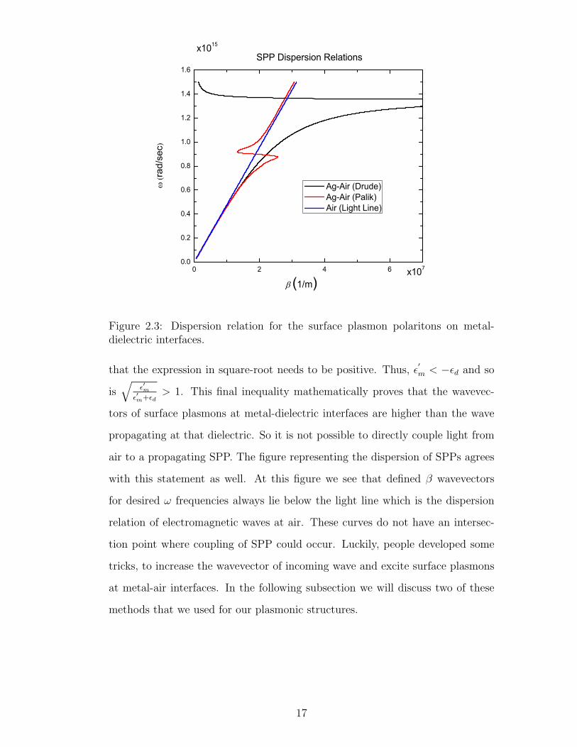
Figure 2.3: Dispersion relation for the surface plasmon polaritons on metal-dielectric interfaces.
that the expression in square-root needs to be positive. Thus, ǫ′
m < −ǫd and so
is√
ǫ′
m
ǫ′
m+ǫd
> 1. This final inequality mathematically proves that the wavevec-
tors of surface plasmons at metal-dielectric interfaces are higher than the wave
propagating at that dielectric. So it is not possible to directly couple light from
air to a propagating SPP. The figure representing the dispersion of SPPs agrees
with this statement as well. At this figure we see that defined β wavevectors
for desired ω frequencies always lie below the light line which is the dispersion
relation of electromagnetic waves at air. These curves do not have an intersec-
tion point where coupling of SPP could occur. Luckily, people developed some
tricks, to increase the wavevector of incoming wave and excite surface plasmons
at metal-air interfaces. In the following subsection we will discuss two of these
methods that we used for our plasmonic structures.
17

2.2 SPP Coupling Techniques
2.2.1 ATR Prism Coupling
Prism coupling with usage of attenuated total reflection (ATR) is the most com-
mon method used for excitation of surface plasmons. The core idea is sending
the light from a high index prism to the thin metal film. When light enters
the prism its wavenumber becomes kp = k0np. The light line of the prism, has
an intersection point with the dispersion curve of surface plasmons on metal-air
interface (figure not given here). This means, if we can satisfy the necessary
conditions we can excite surface plasmons on metal-air interfaces with an optical
wave sent through a prism. There are two main geometries available for this
method, Kretschmann geometry [7] and Otto geometry [6].
Figure 2.4: Different coupling geometries for prism coupling, Kretschmann (a)and Otto (b)
ATR part of this method is also worth mentioning. The incoming light is
totally reflected from a prism metal interface for Kretschmann geometry or from
a prism dielectric interface for Otto geometry. While it is being reflected it
evanescently penetrates into the thin metal layer. This penetrated field oscil-
lates free electrons of metal. If the interaction between the incident wave and
electrons cause coherent oscillations of electrons, surface plasmon resonance con-
dition occurs and the energy of the optical wave couples to surface plasmon waves
18

propagating at the metal dielectric interface. This transfer of energy is monitored
as a dip at the reflection spectrum of incident wave.
The coupling condition for the geometry given at Figure2.4 is
k0npsinθ = kSPP = k0
√
ǫ′mǫd
ǫ′m + ǫd
(2.44)
which means that the horizontal momentum of the incident wave should match
the momentum of the surface plasmon on metal-air interface. The spectrum of
reflected light is given at Figure 2.5.
Figure 2.5: Typical prism coupling scheme. At the spectrum we see the resonancedip, at the field distribution we see the exponential behavior.
2.2.2 Grating Coupling
For the geometries, at which we do not have appropriate geometry to use prism
coupling we use grating coupling instead. When an electromagnetic wave hits on
19
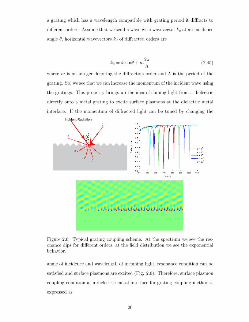
a grating which has a wavelength compatible with grating period it diffracts to
different orders. Assume that we send a wave with wavevector k0 at an incidence
angle θ, horizontal wavevectors kd of diffracted orders are
kd = k0sinθ + m2π
Λ(2.45)
where m is an integer denoting the diffraction order and Λ is the period of the
grating. So, we see that we can increase the momentum of the incident wave using
the gratings. This property brings up the idea of shining light from a dielectric
directly onto a metal grating to excite surface plasmons at the dielectric metal
interface. If the momentum of diffracted light can be tuned by changing the
Figure 2.6: Typical grating coupling scheme. At the spectrum we see the res-onance dips for different orders, at the field distribution we see the exponentialbehavior.
angle of incidence and wavelength of incoming light, resonance condition can be
satisfied and surface plasmons are excited (Fig. 2.6). Therefore, surface plasmon
coupling condition at a dielectric metal interface for grating coupling method is
expressed as
20
2π
λndsinθ + m
2π
Λ=
ω
c
√
ǫ′mǫd
ǫ′m + ǫd
(2.46)
ndsinθ + mλ
Λ= ±
√
ǫ′mǫd
ǫ′m + ǫd
(2.47)
At the prism coupling case the propagation direction of the surface plasmon
is same as the kx wavevector direction of the incident wave. However, for grating
coupling technique we have a number of diffracted orders and these orders can
couple to surface plasmons propagating along forward or backward directions.
This change in direction is represented with the ± sign at Equation 2.47. Oppo-
sitely propagating surface plasmons are shown as splitted resonance dips at the
reflectance spectrum (Fig. 2.6).
21
Chapter 3
OPTICAL DISKS AS SPR
TOOLS
In the previous parts we have given the historical and theoretical background
of plasmonics. We also explained the methods to excite the surface plasmons.
Now it is time for applications. To state again, highly remarkable properties
of surface plasmons are subwavelength confinement of energy, highly sensitive
resonance spectrum based on the change of refractive index and excitation of free
electrons with optical waves. The mentioned properties make plasmonic devices
appropriate for a variety of applications in sensing, optics and optoelectronics.
Due to these potentials, plasmonics continues to draw attention and increasingly
wider availability of high precision fabrication and characterization methods for
submicron metallic structures allows further advances in the field of plasmonics.
For the fabrication and utilization of plasmonic structures there are a number of
methods, where certain geometric properties are dominant in determination of
the conditions for resonant coupling.
In this chapter, we present the method we developed to convert optical disks
(CD, DVD and Blu-Ray) into geometries optimal for study of high quality factor
22

grating coupled plasmon resonances (Fig. 3.1a-b). Previously, CDs and DVDs
have been used in experiments involving grating coupled plasmons [24, 25]. How-
ever, to observe sharp resonances the depth and shape of corrugations must lie
within a restricted range. A sharper resonance improves the overall sensitiv-
ity of plasmonic devices for biomolecular sensing. Moreover, high-Q resonances
result in higher field enhancement factors which is important in a number of
applications such as surface enhanced Raman scattering [26].
(a)
(b)
Figure 3.1: (a) Plasmonic excitation observed on a silver coated DVD surface.The observed coupling occurs at a single polarization and at a specific angle ofincidence. (b) Surface topography by AFM shows the grating structure with aperiod Λ = 740 nm on the DVD.
From the methods described at the previous chapter we used grating coupling
to excite surface plasmons on optical disks. This is a tricky but also an expectable
method because most commercially available optical disks have corrugated im-
printed surfaces protected by external coatings. All we need to do is to tune
23
(a)
(b)
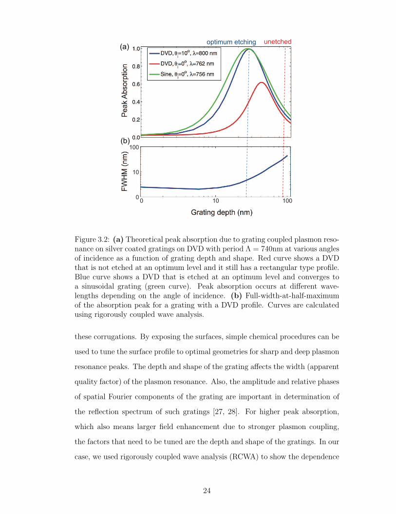
Figure 3.2: (a) Theoretical peak absorption due to grating coupled plasmon reso-nance on silver coated gratings on DVD with period Λ = 740nm at various anglesof incidence as a function of grating depth and shape. Red curve shows a DVDthat is not etched at an optimum level and it still has a rectangular type profile.Blue curve shows a DVD that is etched at an optimum level and converges toa sinusoidal grating (green curve). Peak absorption occurs at different wave-lengths depending on the angle of incidence. (b) Full-width-at-half-maximumof the absorption peak for a grating with a DVD profile. Curves are calculatedusing rigorously coupled wave analysis.
these corrugations. By exposing the surfaces, simple chemical procedures can be
used to tune the surface profile to optimal geometries for sharp and deep plasmon
resonance peaks. The depth and shape of the grating affects the width (apparent
quality factor) of the plasmon resonance. Also, the amplitude and relative phases
of spatial Fourier components of the grating are important in determination of
the reflection spectrum of such gratings [27, 28]. For higher peak absorption,
which also means larger field enhancement due to stronger plasmon coupling,
the factors that need to be tuned are the depth and shape of the gratings. In our
case, we used rigorously coupled wave analysis (RCWA) to show the dependence
24

of peak absorption and quality factor on grating depth for sinusoidal grating
profile and for a quasi-sinusoidal profile commonly observed in DVDs. Results of
calculations are shown in Fig. 3.2a. It is seen that the peak absorption depends
on the sinusoidality of the grating as well as the grating depth. For purely sinu-
soidal gratings, unity absorption is possible at normal incidence. For a grating
with higher order harmonics (as is in a rectangular profile grating), the peak ab-
sorption may never reach unity for certain angles of incidence. Normal incidence
of rectangular profile is shown in Fig. 3.2a where peak absorption can not exceed
0.65 due to coupling of different plasmon modes. However, as the angle is few
degrees away from normal incidence, the absorption can still be close to unity
for optimal grating depths, due to different dispersion of plasmon resonances
associated with higher order harmonics and the fundamental harmonic. Also,
presence of different spatial harmonics of the grating profile causes shifts in the
peak wavelength as denoted in the legend of Fig. 3.2a. The width of resonances
also depend on the grating depth as shown in Fig. 3.2b. Gratings with depths of
20 to 60 nm result in sharp resonances with full-width-at-half-maxima less than
10 nm. Unetched optical disk profiles (typically have 100 nm or more depth for
CD and DVDs) are not optimal for observing sharp and strong resonances. In
most applications it is desirable to have clean, sharp and strong resonances, the
grating depths need to be reduced to an optimal depth and shapes must be made
converged to a sinusoid.
3.1 Modification of optical disk profiles
Optical disks (CD, DVD and Blu-Ray) come in a wide variety of microscopic
structures and use a wide range of materials. In this work, a relatively large
number of disks (CD-R, CD-RW, DVD-R, DVD-RW, Blu-Ray recordable) from
different manufacturers are studied. The rewritable disks (CD-RW and DVD-
RW) generally use a hard chalcogenide material as the recording medium and
25

Blu-Ray write-once disks also use a multilayer hard coating. However, the write-
once CD-R and DVD-R disks use a dye layer as the recording medium that can
be dissolved in weaker solvents. Therefore, we focused on write-once disks for
surface modification. Since different optical disk technologies have different layer
structures, slightly different methods were used to prepare the grating substrates.
CDs have a thin organic coating on top of a metal coating covering the dye layer
and the grating, whereas the DVD-R structure consists of two polycarbonate
disks with spiral grating surfaces in between. Blu-Ray disks have a relatively
thin layer of transparent coating covering the grating layer. Towards the edges
of the disks, the track spirals are well approximated by gratings with periods
of Λ=1600 nm for the CD-R, Λ=740 nm for the DVD-R, and Λ=320 nm for
Blu-Ray.
Figure 3.3: Peeling off procedure for top layer of a CD
For the case of the CD-R, the top protective layer was peeled off by exfoliation
using a tape after delineation of the surface with a sharp cutter. After peeling
off the top surface, the dye layer was removed by washing it with isopropanol.
This procedure was observed not to change the corrugations on the disk but to
26

completely remove the dye. After cleaning, a 4:1 mixture of isopropanol and
acetone was used to etch the grating to the desired depth. Typical etch times
were found to be 10 seconds to few minutes. Slight agitation during etching was
observed to be important for uniform and repeatable etching. Different brands
of commercial CDs were used, and slight differences in corrugation depth and
grating shape as well as differences in etch rates were observed. The surfaces are
then coated with silver films of 50 to 100 nm thickness using thermal vacuum
evaporation. In the case of DVD-R, due to the thick layers that protect the
recording layer, instead of exfoliation by tape, the inner surface was exposed by
first mechanically cutting a notch into the side of the disk and then by applying
mechanical force to peel the two sides apart. Initial cut provides a location
Figure 3.4: Peeling apart procedure for separate layers of a DVD
for separation, which can be initiated from the side by a sharp cutter. The
same procedure that was used for CD-R was also used for cleaning, etching
and metal coating of DVD-R disks. Exposing the Blu-Ray disk gratings were
done by peeling off the transparent thin coating by tweezers after cutting with
27

scissors. Unlike CD-R and DVD-R Blu-Ray disks have nearly sinusoidal grating
shape with 20 nm grating depth which we don’t need to modify and 320 nm
grating period. This grating period brings plasmon resonances at around 320
nm wavelength depending on the angle of incidence. Since silver has enhanced
absorption at this portion of the spectrum we used Al for metal coating of Blu-
Ray.
3.2 Surface plasmons on tuned optical disks
The effect of etching on the topography of CD surfaces are measured using an
AFM (PSIA XE100), as shown in Fig. 3.5a. It can be seen that unetched CD
surfaces have grating profiles nearly rectangular with typical depths of 150 nm.
Since the depth is important for the operation of the CD as an optical disk, dif-
ferent brand disks have similar corrugation depths. It is observed that, etching
in acetone solution reduces the depth of the CD, as well as clearing the higher
frequency components of the profile and changing it to a more sinusoidal shape.
Depending on the choice ambient refractive index, angle of incidence and wave-
length optimal depths for sharp and strong resonances will vary, and must be
calculated. However, typical optimal depths for visible and near infrared wave-
lengths lay in the vicinity of 50 to 90 nm for the CDs. Therefore, 30 to 90 seconds
of etching was found to be adequate.
The reflection spectra are measured using spectroscopic ellipsometry (J. A.
Woollam, VASE) in the visible and infrared wavelengths as shown in Fig. 3.5b,
where progressive appearance of sharp and strong plasmon resonance peaks can
be observed in the reflection spectra. For an unetched substrate, variations in
depth and width along the track lines and non-sinusoidal grating profiles cause
broad and not-so-well defined resonances. However, as the surface is tuned by
etching, sharper resonances appear in the reflection spectra. Also, measurements
28

(a)
(b)
(c)
(d)
Figure 3.5: (a) Topographic profiles of the gratings on CD-R obtained by AFMfor various etching time. (b) Reflection spectra as a function of wavelengths forvarious etching times measured on the CD-R disk coated with 50 nm Silver. (c)Grating coupled plasmon resonance at infrared region observed on CD surfacescoated with 50 nm of silver, at angles of incidence of 40, 45, 50, 55 and 60◦.(d) Rigorously coupled wave analysis results for silver coated CD-R for anglesof incidence 0, 20, 30 and 40◦.
at different angles verify that the dips in the reflection spectra are due to grating
coupled plasmon resonance. The plasmon resonances can also be observed in the
infrared portion of the spectrum. An example of such resonances was observed
using CDs, etched for 30 seconds and coated with a thin (50 nm) layer of silver. In
this configuration, at angles of incidence of 40 to 60 degrees, plasmon resonances
can be observed between 2.4 to 2.8 µm with quality factors of 54 to 30 (Fig. 3.5c).
Figure 3.5d shows the calculated reflection spectra for various incidence angles by
using rigorously coupled wave analysis. The results agree well with measurements
at visible and infrared wavelengths.
For the DVDs, the etched profiles and corresponding reflection spectra are
shown in Fig. 3.6a. The profiles of CDs and DVDs are different in shape. For
most tested CDs, the unetched profiles show nearly symmetric rectangular profile,
29
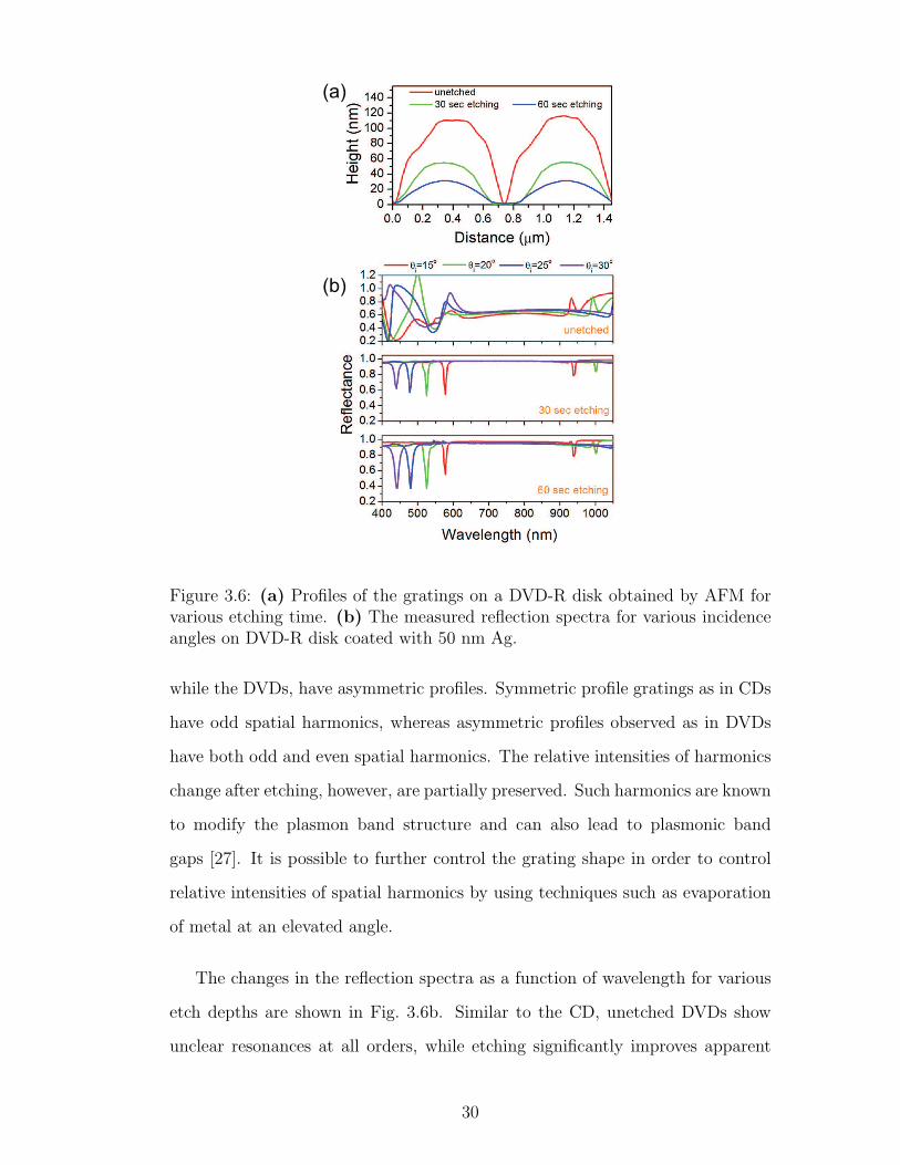
(a)
(b)
Figure 3.6: (a) Profiles of the gratings on a DVD-R disk obtained by AFM forvarious etching time. (b) The measured reflection spectra for various incidenceangles on DVD-R disk coated with 50 nm Ag.
while the DVDs, have asymmetric profiles. Symmetric profile gratings as in CDs
have odd spatial harmonics, whereas asymmetric profiles observed as in DVDs
have both odd and even spatial harmonics. The relative intensities of harmonics
change after etching, however, are partially preserved. Such harmonics are known
to modify the plasmon band structure and can also lead to plasmonic band
gaps [27]. It is possible to further control the grating shape in order to control
relative intensities of spatial harmonics by using techniques such as evaporation
of metal at an elevated angle.
The changes in the reflection spectra as a function of wavelength for various
etch depths are shown in Fig. 3.6b. Similar to the CD, unetched DVDs show
unclear resonances at all orders, while etching significantly improves apparent
30
quality factors of resonances. For example, the full width half maximum for 60
sec etched DVD substrates are from 5 nm to 25 nm for angles of incidence from
15 to 30 degrees. Again, experimentally observed angular dependence of the
resonances agree well with the predictions of Equation 2.45.
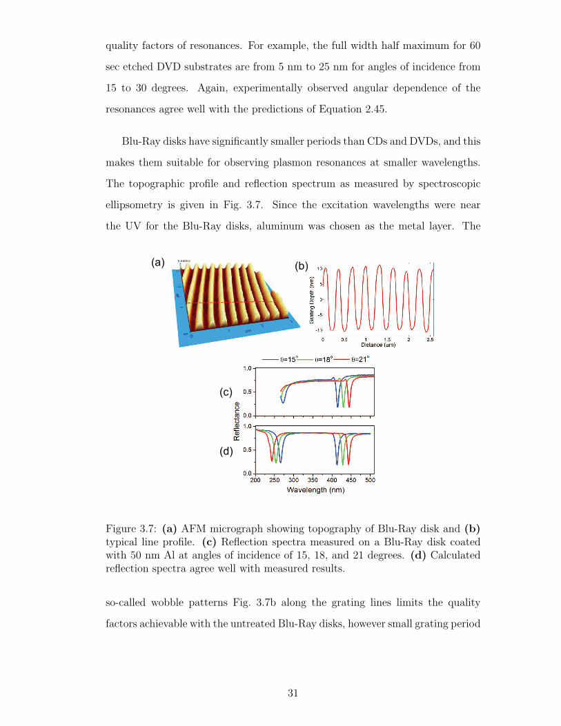
Blu-Ray disks have significantly smaller periods than CDs and DVDs, and this
makes them suitable for observing plasmon resonances at smaller wavelengths.
The topographic profile and reflection spectrum as measured by spectroscopic
ellipsometry is given in Fig. 3.7. Since the excitation wavelengths were near
the UV for the Blu-Ray disks, aluminum was chosen as the metal layer. The
(a) (b)
(c)
(d)
Figure 3.7: (a) AFM micrograph showing topography of Blu-Ray disk and (b)typical line profile. (c) Reflection spectra measured on a Blu-Ray disk coatedwith 50 nm Al at angles of incidence of 15, 18, and 21 degrees. (d) Calculatedreflection spectra agree well with measured results.
so-called wobble patterns Fig. 3.7b along the grating lines limits the quality
factors achievable with the untreated Blu-Ray disks, however small grating period
31

allows excitation of well defined resonances in the UV. Using Al coated Blu-
Ray disks, plasmon resonances can be observed around 300 nm where DNA has
resonant absorption (Fig. 3.7c). Even though measurements are incomplete due
to limitation in the range of ellipsometer below 260 nm wavelengths, calculated
results show distinct plasmonic absorption at UV region (Fig. 3.7d).
3.3 Observation of plasmon resonances in fluids
Once the disks are tuned for sharp resonances, many plasmonic effects and de-
vices based on grating coupled plasmon resonance can be demonstrated. One of
the most common applications of plasmon resonance is in biomolecular sensing.
Such biosensors work by measuring the effective refractive index change due to
molecular adsorption in an aqueous medium . Once functionalized for specific
binding, the surfaces where the plasmon propagates can act as a biomolecular
sensor [13, 14]. We demonstrate such a refractive index measurement setup in a
simple fluid cell as shown in Fig. 3.8a. The shift of the plasmon resonance can
be measured in the angular or wavelength interrogation modes. Using rigorously
coupled wave analysis, reflection spectra of tuned DVD gratings in a fluid cell
geometry can be simulated as is shown in Fig. 3.8b for water and isopropanol as
fluid media for an angle of incidence 15◦. The data shown in Fig. 3.8b shows shift
of the plasmon resonance characterized by a spectroscopic ellipsometer for three
different media, namely deionized water and isopropanol. It is seen that the data
is in agreement with theoretical predictions. In the device configuration shown
in Fig. 3.8a, the refractive index measurement can be performed in the angular
interrogation scheme using a simple silicon photodiode and a simple laser diode.
Although less sensitive compared to prisms in a wavelength interrogation type
measurement [14], the advantage of the use of grating coupled plasmon resonance
for biomolecular sensors is that high index substrates or prisms need not be used,
32

(a)
(b)
Figure 3.8: (a) Configuration used to observe grating coupled plasmon resonancein fluid. (b) Theoretical prediction and experimental data for the fluid beingwater and isopropanol.
and measurements can be performed at normal incidence. In this scheme, opti-
cal disks provide a disposable alternative for high sensitivity plasmon resonance
biomolecular sensors.
Up to now we have shown how to modify optical disks by etching. Alternative
procedures can also be used to modify the topography of optical disk gratings.
Heat treatment (e.g. 150 ◦C , 5 minutes on a hotplate or 140 ◦C, 30 minutes
in an oven) was observed to reflow the grating and produce extremely smooth
sinusoidal gratings of about 30 nm depth, adequate for sharp GCPR lines. How-
ever, unless the disks are placed on flat substrates and unless they are heated
and cooled slowly, flatness of the disks are compromised. As another alternative,
oxygen plasma etching in a parallel plate PECVD system, was also observed to
produce optimal corrugations without disturbing the disk flatness.
33
A pure sinusoidal metal coated grating has no spurious plasmon resonances
and, the presented procedure does not produce perfectly sinusoidal surfaces.
However, the tuned gratings are shown to behave like ideal sinusoidal gratings,
for a wide range of incidence angles. The deviations from ideal sinusoids, can be
observed in the reflection spectra. For example, the effect of wobble patterns and
deviations from a pure sinusoid have been observed as a limitation in the peak
absorption and widths of the resonances. Chemical etch tuning of the CD and
DVDs were observed to reduce the effect of such secondary patterns. It was also
observed that, a low surface roughness metal coating is important for observing
higher quality factors. The surface roughness of silver layers can be increased
by rapid metal evaporation. However, by reducing the evaporation rate or using
sputter coating, smoother silver surfaces can be obtained, increasing the quality
factors of resonances.
3.4 Demonstration of a Plasmonic Filter with
Optical Discs
Although plasmonic structures have been extensively studied for better un-
derstanding of fundamental physical phenomenon, optoelectronic device ap-
plications generally focused on sensors. Since the pioneering works of Ebbe-
sen [15] and Ghaemi [29] transmission of electromagnetic waves through thin
metal films via plasmons has widely been studied. Plasmon resonance en-
hanced transmission through subwavelength holes, hole arrays or periodically
corrugated metal surfaces have been investigated both theoretically and exper-
imentally [30, 31, 32, 33]. The resonant transmission peaks due to interacting
plasmonic structures (weak coupling regime) have been observed in Silver films
containing an array of Silicon spheres [34]. Optical properties of the periodic
34

arrays of defects (voids) in mesoporous metals [35] and two-dimensional metallic
quasi-photonic crystals [36] have also been investigated.
In this section we will explain how we could obtain plasmonic filters, that
gives us sharp transmission peaks in coupled surface-plasmon on metallized grat-
ing structures. The grating structures are again obtained from optical storage
disks. A filter based on plasmon enhanced transmission (PET) in metal coated
coupled-grating structures is proposed and experimentally demonstrated. The fil-
ter consists of two metallized gratings placed back-to-back as shown in Fig. 3.9a.
In an optimized layer structure with sufficiently thin metal layer, light is partially
(a)
(b)
Figure 3.9: (a) Scheme of proposed filter structure. Top and bottom surfacesare parallel to each other. Both have the same grating period and silver coatedon them is at the same thickness. (b) Calculated H field component of EM wavethrough coupled plasmonic structure agrees well with proposed scheme. Insetshows the plasmonic radiation from sinusoidal grating.
35

transmitted through the metal layer and is partially diffracted or re-emitted into
different orders with different angles of propagation. For our proposed struc-
ture, the transmitted orders travel inside the substrate and are incident onto an
identical grating on the other face of the substrate. Due to the symmetry of
the device, components of the light wave that are generated through plasmonic
emission recouple to the plasmon mode and a second event of plasmon enhanced
transmission takes place at the second grating.
The distance between the two surfaces carrying the gratings, t, is very large
compared to the plasmon propagation length and free space wavelength (t ≫ ξ,
λ). Under this condition, the reflected waves from the second surface do not
interfere with (regenerate) the plasmons on the first surface, hence our analysis
remains valid.
Figure 3.9b shows the calculated field distribution through the device for
wavelength λ = 580 nm and angle of incidence θi = 15◦ (Λ = 740 nm and
Λ ≪ t). It can be seen that the electromagnetic (EM) waves are re-emitted from
second grating layer at the same angle of incidence as the incoming wave. Even
though the dielectric layer thickness between the gratings is order of 1mm in
real device structures, it is taken 10 µm to avoid computational difficulties in
the finite difference time domain (FDTD) simulations. In this case, t is much
larger than the wavelength of light of incident beam, but it is comparable to the
plasmon propagation length.
Since our aim in this research is filter design, we first examined the transmis-
sion intensity through a single layer of silver-coated grating with Λ = 740 nm as a
function of metal thickness (Fig. 3.10a) and wavelength (Fig. 3.10b) of incoming
wave by using rigorously coupled wave analysis (RCWA).
As shown in Fig. 3.10a, the transmitted power for +1st diffraction order
reaches its maximum value near 45 nm silver thickness for TM waves. On the
36

Figure 3.10: (a) Transmitted fraction of light on resonance as a function of metalthickness for incidence angle θ = 10◦ and λ = 630 nm. Since TE mode is notresonantly transmitted, the filter also acts as a polarizer, transmitting mainly TMpolarization. Optimal Ag thickness is seen to be about 45 nm. (b) Transmittedfraction of light as a function of wavelength for the −1st, 0th and +1st diffractionorders, for incidence angle θ = 10◦ and tAg = 45 nm
other hand, the transmitted intensity for all the other diffracted orders for TE
and TM waves are an order of magnitude smaller. Figure 3.10b shows wavelength
dependence of transmitted power for different diffraction orders of both TE and
TM modes. The maximum value of the +1st diffraction order for TM mode for
incidence angle θi = 10◦ occurs at wavelength λ = 628 nm. The filter acts also
as a polarizer, with a TM/TE polarization ratio of about 100. This TM/TE
ratio lets us think that this transmission might be due to the excited plasmon
oscillations in the metal.
37

In order to implement our filter structure, we again used gratings present on
optical storage disks. Surface modification of optical disks is again done with the
same method described above. After this grating depth modification treatment
two such surfaces are fixed back-to-back using a thin UV curable epoxy layer.
Then the surfaces are metallized by vacuum evaporation of a 45 nm thick silver
layer. A similar procedure was repeated using a CD, where the grating depth
was tuned to 60 nm. The transmission through the structures were measured
using spectrometric ellipsometers (J. A. Woollam VASE) in the visible and in
the near infrared.
Figure 3.11: (a) Calculated reflection, transmission and absorption spectra as afunction of wavelength for TM waves. Calculation parameters are grating periodΛ = 740 nm, silver thickness tAg = 45 nm and incidence angle θ = 15circ. (b)Comparison of measured and calculated transmittance as a function of wave-length. Finite resolution of the spectrometer partially explains the discrepancybetween calculations and measurement around 950 nm.
The total transmission through the coupled plasmonic grating structure as a
function of wavelength for 15◦ angle of incidence is calculated by using RCWA
and is shown in Fig. 3.11a, where Λ = 740 nm. The measured transmittance
through the filter for θi = 15◦ shows peak at wavelengths λ = 580 nm and
940 nm. As shown in Fig. 3.11b, the simulations explain the measured spectra
quantitatively if a finite spectrometer resolution is assumed.
38

Besides the theoretical prediction of transmittance we also performed FDTD
simulations and experimentally measured the transmittance through the pro-
posed plasmonic filter for various incidence angles ranging from θi = 0◦ to 20◦
(Fig. 3.12). It can be seen that, a peak transmission of up to 0.17 can be achieved
(a)
(b)
Figure 3.12: Transmitted intensity of a device having a grating period of Λ = 740nm and t = 1 mm at various angles of incidence, as measured with a spectroscopicellipsometer.(a) Simulation results, (b) Experimental measurements
experimentally over a broad wavelength range, with full width at half maximum
(FWHM) of 10 to 5 nm. The positions of the experimental peaks agree well
with the predictions of RCWA and FDTD simulations. For instance, the results
shown at Fig. 3.2 predicts the transmission peak to occur at λ = 628 nm for
45 nm thick Ag coated grating and 10◦ of incidence angle, at the experiment
39

we obtain the transmission peak at λ = 635 nm for the same structure. At the
FDTD simulations 0◦ simulations is exactly the same as the experimental mea-
surements. However, when we move to higher angles we have a little deviation.
This deviation is the result of boundary conditions set for FDTD. For 0◦ we used
Bloch boundary conditions with only one period sample, when we increased the
incident angle we moved on to periodic boundary conditions with larger samples.
For the device fabricated using CDs with grating periods of Λ = 1600 nm,
plasmon enhanced transmission (PET) phenomenon can be observed in the near
infrared portion of the spectrum at angles of incidence close to normal, as shown
in Fig. 3.13. Due to finite transmission of the CD material (characterized by
Fourier Transform Infrared (FTIR) spectrometer, data not shown), and rela-
tively large thickness of the double CD substrate (3 mm), total transmission at
Figure 3.13: Measured transmitted intensity of a device having a grating periodof Λ = 1600 nm (built on a CD) at various angles of incidence
the resonant wavelength is reduced to few percent. However, well defined reso-
nances with widths of about 50 nm can be observed. This corresponds to a peak
40

wavelength to width ratio of about 40, which compares favorably with previously
reported PETs at similar wavelengths.
In summary we proposed and demonstrated an optical filter that uses plas-
mon enhanced transmission through metallized gratings. The devices are real-
ized using optical disks as starting substrates. Sharp transmission peaks with
peak wavelengths dependent on the angle of incidence make the devices suitable
for applications in compact spectrometers. By fabricating the device using an
elastomeric substrate, peak wavelength can be tuned by applying strain. Theo-
retical calculations and measurements predict that such devices can be operated
at infrared wavelengths by proper scaling. When used to filter collimated ther-
mal emission, devices can be used to fabricate tunable, polarized infrared light
sources, or disposable infrared spectrometers. It would be interesting to investi-
gate an array of coupled plasmonic structures by varying the distance between
plasmonic gratings.
41

Chapter 4
SURFACE PLASMONS AT
MIM WAVEGUIDES
The work we will show at this chapter contains excitation of surface plasmons
at metal-insulator-metal (MIM) systems. The question is, why should MIM
plasmonic systems be an interesting research topic and what do we aim by that
research?
4.1 An MIM Surface Plasmon Waveguide
From Chapter 2 we know that we have to have a resonance condition for exci-
tation of surface plasmons. Again at Chapter 2 we saw that this resonance is
observed as a single dip at the reflection spectrum. This single dip is the only
mode of surface plasmon waveguide. Also from waveguide theory we know that
if a system had more than one mode, each of these modes would correspond
to a different field profile distribution at the system. Basing on the work of
Bayindir [37], we presumed that if we perturb a stable system in some way and
increase its modes from one to two, these two modes correspond to bonding and
42
anti-bonding modes of systems and the field profile observed becomes symmetric
and anti-symmetric for each of these modes.
Final justification is why we need symmetric and anti-symmetric field distri-
butions. By having such oppositely distributed field distributions we expected to
obtain attractive and repulsive forces between metal layers. If we could calculate
this force we would call it plasmonic force, but at this chapter we will just be
concerned with excitation of these modes with numerical tools.
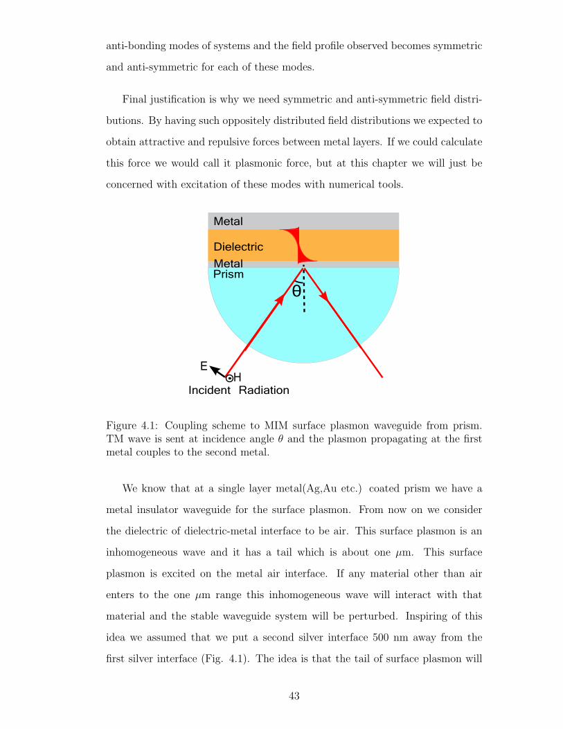
Figure 4.1: Coupling scheme to MIM surface plasmon waveguide from prism.TM wave is sent at incidence angle θ and the plasmon propagating at the firstmetal couples to the second metal.
We know that at a single layer metal(Ag,Au etc.) coated prism we have a
metal insulator waveguide for the surface plasmon. From now on we consider
the dielectric of dielectric-metal interface to be air. This surface plasmon is an
inhomogeneous wave and it has a tail which is about one µm. This surface
plasmon is excited on the metal air interface. If any material other than air
enters to the one µm range this inhomogeneous wave will interact with that
material and the stable waveguide system will be perturbed. Inspiring of this
idea we assumed that we put a second silver interface 500 nm away from the
first silver interface (Fig. 4.1). The idea is that the tail of surface plasmon will
43

penetrate into the second interface and it will oscillate the electrons of that silver
coherently as well. From the interaction of two excited electron oscillations we
might be able to excite more than one modes of the system.
For this system design we have some selection criteria. We took the prism
material as SiO2. We used silver as the metal due to its allowance for sharper
resonances. Thickness of first silver layer is 50 nm due to plasmon excitation,
second silver layer is taken as 300 nm thick. Why is the second layer thicker
question may arise here. If we took second layer as 50 nm as well, surface plasmon
wave penetrates all into the second metal and we get three modes excited (will
be shown at the following subsections). That is why we select it 300 nm in
our simulations. The 500 nm distance is predictably due to create a stronger
interaction between the layers.
4.2 Theoretical Simulations
For the investigation of this system we used two approaches. One is simulation
using Fresnel’s multilayer reflection theory, second is FDTD method. At the
Fresnel’s equations part we used the formula for reflection at a single interface and
we iteratively introduced it to multilayer reflection theory. Numerically speaking
for a two layer system with respect to Figure 3.1 with dielectric constants ǫi and
ǫj, wave numbers ki and kj which correspond to kd and km with respect to Eqn
3.33 and Eqn 3.34
rij =
(
ki
ǫi
−kj
ǫj
)
/
(
ki
ǫi
+kj
ǫj
)
(4.1)
This equation is valid if there is only one interface. For our case 4.2, due to
the interference effects we should take the third layer into account as well. This
gives us a reflection coefficient
44

Figure 4.2: Fresnel coefficients for transmitted and reflected waves at the multi-layered material geometries. The numbers of materials are given as a referenceto Equation4.2
r012 =r01 + r12e
2iα
1 + r01r12e2iα(4.2)
with α = k1d1.
We coded these formulas in MATLAB and obtained our theoretical simulation
results. For our simulations we started from the end, where we have infinite air,
and iteratively came to the prism part. So we have become able to simulate multi
layer structures without an upper limit e.g. IMI....MIM structures. A sample
graph taken for MIM case is given at Figure 4.3. For the single layer Ag part
we assumed 60 nm Ag coated on a prism with refractive index np = 1.8. The
wavelength of the incident light is set to λ = 500 nm. With these circumstances
we obtained the resonance at 36.1◦. Then we have put one more Ag layer 700
nm away from the first layer and we got the second graph. At this figure we can
clearly see that first stable mode is perturbed from new Ag and we can see the
splitting at the spectrum.
45

Figure 4.3: Observation of splitting phenomenon at theoretical simulations.Spectrum is scanned by changing incidence angle θ. Distance between layersd = 700 nm, wavelength λ = 500 nm and np = 1.8.
From this figure we can also deduce that the mode at the beginning is com-
pletely disappeared. If we were to send light again with incidence angle 36.1◦ we
would get 80% reflectance i.e. non resonant situation.
A similar behavior is also seen at the frequency spectrum. While examining
wavelength dependence we can also verify that this change at modes is due to
perturbation. This is possible by looking at the spectrum change at different
dielectric distances. At the simulation results given at Figure 4.4 we examined
the dielectric thickness dependence from the wavelength spectrum perspective.
Incident angle for this simulation is set to θ = 43.6◦. When the system is
not perturbed we have a single dip at 633 nm. When we bring second Ag layer
closer we see the mode separation at about 1800 nm distance. When we shrink
the distance we create a more powerful interaction between second metal and
46

the system. Due to this powerful interaction we see a wider separation of modes
at the spectrum.
Figure 4.4: Effect of distance between layers, to splitting amount between themodes. As we see, while distance is decreasing, splitting at spectrum is increas-ing. This is what we expected due to stronger interaction at closer distances.
Now, it is also a good time to verify what we claimed about the thickness of
the second metal. We said that for observing a more accurate splitting we had
better use a thick (more that 200-300 nm) metal. We also claimed that if we
used a thinner (50-100nm) metal as the second layer we would observe excitation
of fundamental mode again at the system. The graph at Figure4.5 explains the
situation better. At this figure the red curve shows the non-perturbed system.
When we introduce a thick (200 nm) Ag metal to the system we observe the
splitting (black curve) at the incident angle dependence. If we use a thin (70
nm) metal instead fundamental mode is again excited and this is not a case we
would like. If we used even thinner metals (50 nm) the fundamental mode also
47

Figure 4.5: Observation of spectrum with respect to thickness of second metallayer. As we see when it is not thick enough it sustains two plasmon modes andone of them is the fundamental mode, and it perturbs the MIM splitting.
disturbs other modes’ resonance angles. For that reason we preferred using thick
metals.
4.3 FDTD Simulations
For the verification of what we theoretically presumed we need to show it exper-
imentally. However, fabrication of the proposed device was not that easy. We
have fabricated Ag bridge structures on a SiO2 glass. Before fixing these glasses
to the prism we etched the sacrificial layer to use air as the insulating material.
At our etching trials we could not obtain an optimum MIM waveguide. Since the
experiment way was partially closed we chose verification by FDTD simulations,
which I call experimental simulations.
48
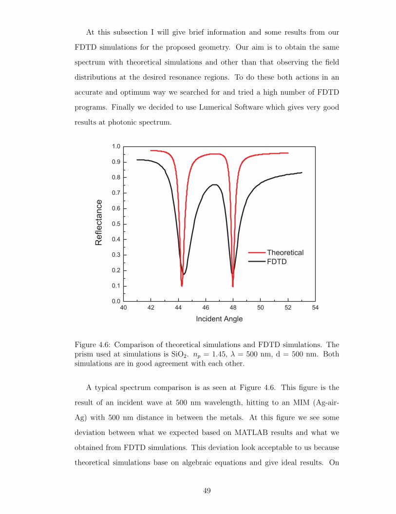
At this subsection I will give brief information and some results from our
FDTD simulations for the proposed geometry. Our aim is to obtain the same
spectrum with theoretical simulations and other than that observing the field
distributions at the desired resonance regions. To do these both actions in an
accurate and optimum way we searched for and tried a high number of FDTD
programs. Finally we decided to use Lumerical Software which gives very good
results at photonic spectrum.
Figure 4.6: Comparison of theoretical simulations and FDTD simulations. Theprism used at simulations is SiO2. np = 1.45, λ = 500 nm, d = 500 nm. Bothsimulations are in good agreement with each other.
A typical spectrum comparison is as seen at Figure 4.6. This figure is the
result of an incident wave at 500 nm wavelength, hitting to an MIM (Ag-air-
Ag) with 500 nm distance in between the metals. At this figure we see some
deviation between what we expected based on MATLAB results and what we
obtained from FDTD simulations. This deviation look acceptable to us because
theoretical simulations base on algebraic equations and give ideal results. On
49

the other hand, FDTD softwares divide the space into finite little areas and give
an approximation to the experiment. And this approximation might create little
deviations at both spectrum or intensity of electromagnetic waves.
(a)
(b)
Figure 4.7: Field profile results of FDTD simulations. We observe the excited
symmetric and anti-symmetric behaviors of surface plasmon waves clearly. (a)
symmetric distribution at θ = 44.4◦ and (b) anti-symmetric distribution at θ =
47.95◦
On the other hand the important thing is that the spectral places of the
resonance dips are very strongly correlated and there is very little deviation from
50
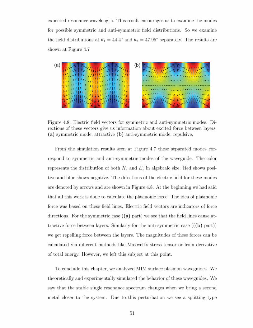
expected resonance wavelength. This result encourages us to examine the modes
for possible symmetric and anti-symmetric field distributions. So we examine
the field distributions at θ1 = 44.4◦ and θ2 = 47.95◦ separately. The results are
shown at Figure 4.7
(b)(a)
Figure 4.8: Electric field vectors for symmetric and anti-symmetric modes. Di-rections of these vectors give us information about excited force between layers.(a) symmetric mode, attractive (b) anti-symmetric mode, repulsive.
From the simulation results seen at Figure 4.7 these separated modes cor-
respond to symmetric and anti-symmetric modes of the waveguide. The color
represents the distribution of both Hz and Ex in algebraic size. Red shows posi-
tive and blue shows negative. The directions of the electric field for these modes
are denoted by arrows and are shown in Figure 4.8. At the beginning we had said
that all this work is done to calculate the plasmonic force. The idea of plasmonic
force was based on these field lines. Electric field vectors are indicators of force
directions. For the symmetric case ((a) part) we see that the field lines cause at-
tractive force between layers. Similarly for the anti-symmetric case (((b) part))
we get repelling force between the layers. The magnitudes of these forces can be
calculated via different methods like Maxwell’s stress tensor or from derivative
of total energy. However, we left this subject at this point.
To conclude this chapter, we analyzed MIM surface plasmon waveguides. We
theoretically and experimentally simulated the behavior of these waveguides. We
saw that the stable single resonance spectrum changes when we bring a second
metal closer to the system. Due to this perturbation we see a splitting type
51

behavior at the spectrum. When we have a closer look to these splitted modes
we see that they are symmetric and anti-symmetric field distributions. These
field distributions cause a force between the layers, calculation of which is left as
future work.
52

Chapter 5
CONCLUSIONS
At this thesis we studied plasmonics at a number of different applications. First
of all we used surface modified optical disks for excitation of surface plasmons.
With this method we aimed to provide a compact working environment for plas-
monics. We could realize grating coupling method efficiently, without using an
interference lithography type fabrication procedure. We have shown how to etch
the surfaces of optical disks and how this etching procedure affects the resonance
quality. Since different disks have different grating periods we could achieve
plasmon resonances at a wide spectrum ranging from UV to NIR.
Then we tried an application with this modified optical disks. At the simu-
lations we have seen that light passes through thin layers of metal at resonance
condition. This gave us inspiration to design a filter from these disks. We fabri-
cated a device, with optimum gratings at both sides which are metal-coated. We
verified our design with numerical simulations and experimental measurements.
So we obtained an optical filter, the spectrum of which is wavelength, polariza-
tion and incident angle dependent. The transmission peaks of the filter could
achieve quality factors as high as 100.
53

We finally worked on MIM waveguides for surface plasmons. At this part we
examined the perturbation effect when we bring a metal close to a metal insulator
waveguide. We observed a splitting at the spectrum due to perturbation. This
splitting corresponded to bonding and antibonding modes of the system. So we
expected to observe different field profiles at these separate modes and at the
simulations we saw that these modes have symmetric and anti-symmetric field
distributions respectively. Different field distributions suggest an excited force
between metals, which we named plasmonic force.
54

Bibliography
[1] E. Hecht, Optics. Addison Wesley, San Francisco, 2003.
[2] R. D. Guenther, Modern Optics. John Wiley & Sons, New York, 1983.
[3] R. W. Wood, “On a remarkable case of uneven distribution of light in
a diffraction grating spectrum,” Proc. Phys. Soc. London, vol. 18, no. 1,
pp. 269–275, 1902.
[4] U. Fano, “The theory of anomalous diffraction gratings and of quasi-
stationary waves on metallic surfaces,” J. Opt. Soc. Am., vol. 31, pp. 213–
222, 1941.
[5] T. Turbadar, “Complete absorption of light by thin metal films,” Proc. Phys.
Soc., vol. 73, pp. 40–44, 1959.
[6] A. Otto, “Towards multimaterial multifunctional fibres that see, hear, sense
and communicate,” Zeitschrift fur Physik, vol. 216, pp. 398–410, 1968.
[7] E. Kretschmann and H. Raether, “Dynamic all-optical tuning of trans-
verse resonantcavity modes in photonic bandgap fibers,” Z Naturforschung,
vol. 23a, p. 2135, 1968.
[8] W. L. Barnes, A. Dereux, and T. W. Ebbesen, “Surface plasmon subwave-
length optics,” Nature, vol. 424, pp. 824–830, 2003.
[9] E. Ozbay, “Plasmonics: Merging photonics and electronics at nanoscale
dimensions,” Science, vol. 311, pp. 189–193, 2006.
55

[10] H. Atwater, “Promise of plasmonics,” Scientific American, pp. 56–63, April
2009.
[11] J. C. Quail, J. G. Rako, H. J. Simonand, and R. T. Deck, “Optical second-
harmonic generation with long-range surface plasmons,” Phys. Rev. Lett.,
vol. 50, pp. 1987–1989, 1983.
[12] N. C. Panoiu and R. M. Osgood, “Subwavelength nonlinear plasmonic
nanowire,” Nano Lett., vol. 4, pp. 2427–2430, 2004.
[13] J. Homola, “Surface plasmon resonance sensors for detection of chemical
and biological species,” Chem. Rev., vol. 108, pp. 462–493, 2008.
[14] J. Homola, S. S. Yee, and G. Gauglitz, “Surface plasmon resonance sensors:
review,” Sensors and Actuators B, vol. 54, pp. 3–15, 1999.
[15] T. W. Ebbesen, H. J. Lezec, H. F. Ghaemi, T. Thio, and P. A. Wolff,
“Extraordinary optical transmission through sub-wavelength hole arrays,”
Nature, vol. 391, pp. 667–669, 1998.
[16] J. A. Dionne, L. A. Sweatlock, H. A. Atwater, and A. Polman, “Plasmon
slot waveguides: Towards chip-scale propagation with subwavelength-scale
localization,” Phys. Rev. B, vol. 73, pp. 035407(1)–035407(9), 2006.
[17] H. T. Miyazaki, “Squeezing visible lightwaves into a 3-nm-thick and 55-nm-
long plasmon cavity,” Phys. Rev. Lett., vol. 96, pp. 097401(1)–097401(4),
2006.
[18] T. Kurokawa and H. T. Miyazaki, “Metal-insulator-metal plasmon nanocav-
ities: Analysis of optical properties,” Phys. Rev. B, vol. 75, pp. 035411(1)–
035411(13), 2007.
[19] B. Kaplan, H. Guner, O. Senlik, K. Gurel, M. Bayindir, and A. Dana,
“Tuning optical disks for plasmonic applications,” Plasmonics, 2009.
56

[20] K. Gurel, B. Kaplan, H. Guner, M. Bayindir, and A. Dana, “Resonant
transmission of light through surface plasmon structures,” Applied Physics
Letters, vol. 94, p. 233102, 2009.
[21] P. Drude, “Zur elektronentheorie der metalle.,” Ann. Phys., vol. 1, pp. 566–
613, 1900.
[22] P. B. Johnson and R. W. Christy, “Optical constants of the noble metals.,”
Phys. Rev. B, vol. 6, pp. 4370–4379, 1972.
[23] S. A. Maier, Plasmonics Fundamentals and Applications. Springer, 2007.
[24] E. Fontana, “Theoretical and ecperimental study of the surface plasmon
resonance on a recordable compact disk,” Appl Opt, vol. 43, pp. 79–87,
2004.
[25] N. Sedoglavich, R. Kunnemeyer, S. R. Dalele, and J. Sharpe, “Phase-
polarization contrast for surface plasmon resonance based on low cost grat-
ing substrates,” Current Applied Physics, vol. 8, pp. 351–354, 2008.
[26] K. Kneipp, H. Kneipp, I. Itzkan, R. R. Dasari, and M. S. Feld, “Surface
enhanced raman scattering and biophysics.,” J Phys Chem, vol. 14, pp. 597–
624, 2002.
[27] A. Kocabas, G. Ertas, S. S. Senlik, and A. Aydinli, “Plasmonic band gap
structures for surface-enhanced raman scattering,” Opt Express, vol. 16,
pp. 12469–12477, 2008.
[28] A. Kocabas, S. S. Senlik, and A. Aydinli, “Plasmonic band gap cavities on
biharmonic gratings,” Phys Rev B, vol. 77, no. 19, pp. 195130(1)–195130(7),
2008.
[29] F. Ghaemi, T. Thio, D. E. Grupp, T. W. Ebbesen, and H. J. Lezec, “Surface
plasmons enhance optical transmission through subwavelength holes,” Phys
Rev B, vol. 58, p. 6779, 1998.
57
[30] I. Avrutsky, Y. Zhao, and V. Kochergin, “Surface-plasmon-assisted resonant
tunneling of light through a periodically corrugated thin metal film,” Opt
Lett, vol. 25, pp. 595–597, 2000.
[31] N. Bonod, S. Enoch, L. Li, E. Popov, and M. Neviere, “Resonant opti-
cal transmission through thin metallic films with and without holes,” Opt
Express, vol. 11, pp. 482–490, 2003.
[32] Y.-H. Ye and J.-Y. Zhang, “Enhanced light transmission through cascaded
metal films perforated with periodic hole arrays,” Opt Lett, vol. 30, pp. 1521–
1523, 2005.
[33] H. E. Went, A. P. Hibbins, J. R. Sambles, C. R. Lawrence, and A. P. Crick,
“Selective transmission through very deep zero-order metallic gratings at
microwave frequencies,” App Phys Lett, vol. 77, p. 2789, 2000.
[34] F. J. G. de Abajo, G. Gomez-Santos, L. A. Blanco, A. G. Borisov, and S. V.
Shabanov, “Tunneling mechanism of light transmission through metallic
films,” Phys Rev Lett, vol. 95, p. 067403, 2005.
[35] N. Stefanou, A. Modinos, and V. Yannopapas, “Optical transparency of
mesoporous metals,” Solid State Commun., vol. 118, p. 69, 2001.
[36] M. Bayindir, E. Cubukcu, I. Bulu, and E. Ozbay Europhys. Lett., vol. 56,
p. 41, 2001.
[37] M. Bayindir, B. Temelkuran, and E. Ozbay, “Tight-binding description of
the coupled defect modes in three-dimensional photonic crystals,” Phys Rev
B, vol. 84, pp. 2140–2143, 2000.
58