Embed Size (px)
Citation preview
Coupled effects in PDE-based modelsfor nanoscience
Roderick Melnik
BCAM, Bizkaia Technology Park, 48160 Derio, Spain &
Wilfrid Laurier University and University of Waterloo,
Waterloo, ON, Canada, N2L 3C5
http://www.m2netlab.wlu.ca
Basque Center for Applied Mathematics - WGLR1
July 8, 2010
Coupled effects in PDE-based modelsfor nanoscience – p.1/36

Outline of This Talk
� Mathematical Models for Low-Dimensional Nanostructures (LDN).
� A hierarchy of physics-based models as a key ingredient of the
validation process.
The process of LDN formation and consequences for modelling.
� Geometric and materials nonlinearities; coupled effects and a
hierarchy of mathematical models.
� Variational formulation and coupling procedures: piezo-, thermal, and
magnetic fields.
� Higher order nonlinear effects: electrostriction and phase
transformations.
� Modelling RNA nanostructures.
� Concluding remarksCoupled effects in PDE-based modelsfor nanoscience – p.2/36

Introduction
� Low dimensional (semiconductor) nanostructures:quantum wells, quantum wires, quantum dots.
� Linear Schrodinger model in the steady-stateapproximation.
� New technological advances in applications oflow-dimensional semiconductor nanostructures(LDSN).
� Experiments by [Zaslavsky et al]: effects at differentscales that may influence substantiallyoptoelectromechanical properties of thenanostructures - strain relaxation, piezo-, thermaleffects...
Coupled effects in PDE-based modelsfor nanoscience – p.3/36
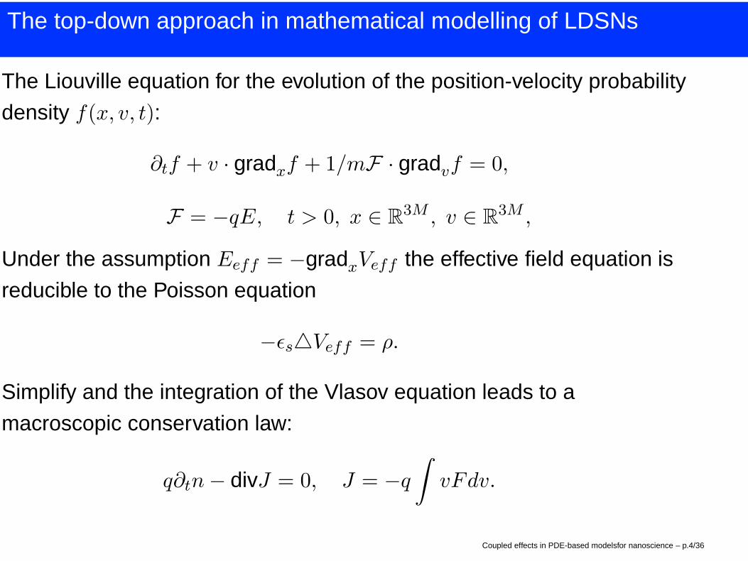
The top-down approach in mathematical modelling of LDSNs
The Liouville equation for the evolution of the position-velocity probability
density f(x, v, t):
∂tf + v · gradxf + 1/mF · gradvf = 0,
F = −qE, t > 0, x ∈ R3M , v ∈ R
3M ,
Under the assumption Eeff = −gradxVeff the effective field equation is
reducible to the Poisson equation
−ǫs△Veff = ρ.
Simplify and the integration of the Vlasov equation leads to a
macroscopic conservation law:
q∂tn− divJ = 0, J = −q
∫
vFdv.
Coupled effects in PDE-based modelsfor nanoscience – p.4/36
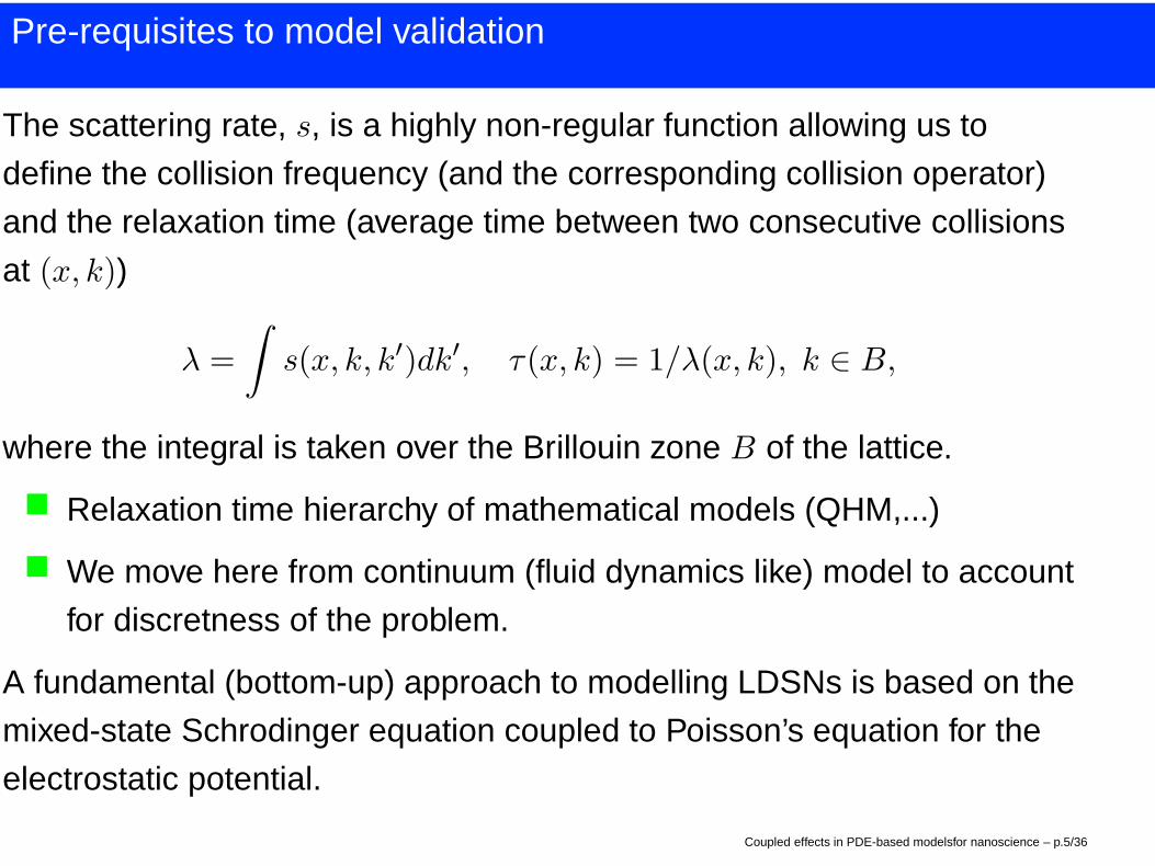
Pre-requisites to model validation
The scattering rate, s, is a highly non-regular function allowing us to
define the collision frequency (and the corresponding collision operator)
and the relaxation time (average time between two consecutive collisions
at (x, k))
λ =
∫
s(x, k, k′)dk′, τ(x, k) = 1/λ(x, k), k ∈ B,
where the integral is taken over the Brillouin zone B of the lattice.
� Relaxation time hierarchy of mathematical models (QHM,...)
� We move here from continuum (fluid dynamics like) model to account
for discretness of the problem.
A fundamental (bottom-up) approach to modelling LDSNs is based on the
mixed-state Schrodinger equation coupled to Poisson’s equation for the
electrostatic potential.
Coupled effects in PDE-based modelsfor nanoscience – p.5/36

Realities of the bottom-up approach: the process of QD formation
The formation of LDSNs (in particular quantum dots) is acompetition between the surface energy in the structure andstrain energy.
Technologically, all effective methodologies are basedon self-assembly where the final result is often many(dozens and even hundreds) self-assembled dots sitting on t hewetting layer and randomly distributed over it , having� different size,� shape, and, ultimately,� properties.
Coupled effects in PDE-based modelsfor nanoscience – p.6/36

Isolated QDs vs QD arrays
Figure 1: AFM image of quantum dots grown on Si substrate of 4.1
monolayers with optimized growth conditions [WB, PC Sharma].Coupled effects in PDE-based modelsfor nanoscience – p.7/36
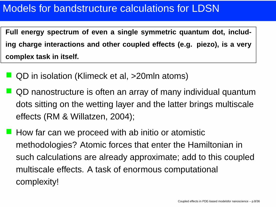
Models for bandstructure calculations for LDSN
Full energy spectrum of even a single symmetric quantum dot, includ-
ing charge interactions and other coupled effects (e.g. pie zo), is a very
complex task in itself.
� QD in isolation (Klimeck et al, >20mln atoms)
� QD nanostructure is often an array of many individual quantumdots sitting on the wetting layer and the latter brings multiscaleeffects (RM & Willatzen, 2004);
� How far can we proceed with ab initio or atomisticmethodologies? Atomic forces that enter the Hamiltonian insuch calculations are already approximate; add to this coupledmultiscale effects. A task of enormous computationalcomplexity!
Coupled effects in PDE-based modelsfor nanoscience – p.8/36

Averaging procedures
We need some averaging over atomic scales :
� empirical tight-binding,� pseudopotential, and� k · p approximations.
The k · p (envelope function) theory represents the electronicstructure in a continuum-like manner and is well suited forincorporating additional effects into the model such as str ainand piezoelectric and other coupled effects, including hig herorder nonlinear effects.
Coupled effects in PDE-based modelsfor nanoscience – p.9/36
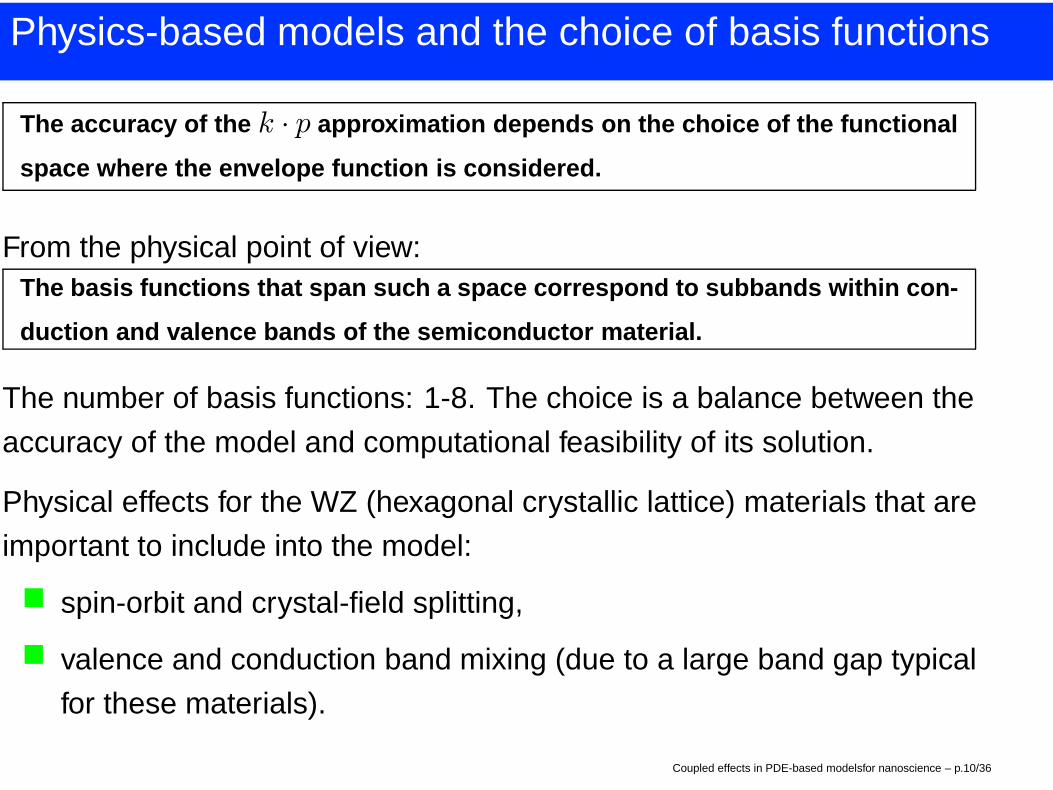
Physics-based models and the choice of basis functions
The accuracy of the k · p approximation depends on the choice of the functional
space where the envelope function is considered.
From the physical point of view:The basis functions that span such a space correspond to subb ands within con-
duction and valence bands of the semiconductor material.
The number of basis functions: 1-8. The choice is a balance between the
accuracy of the model and computational feasibility of its solution.
Physical effects for the WZ (hexagonal crystallic lattice) materials that are
important to include into the model:
� spin-orbit and crystal-field splitting,
� valence and conduction band mixing (due to a large band gap typical
for these materials).
Coupled effects in PDE-based modelsfor nanoscience – p.10/36

The model for the WZ materials
The model, in its general setting, is based on 6 valence subbands and 2
conduction subbands (accounting for spin up and down situations) and
we need to solve the following PDE eigenvalue problem with respect to
eigenpair (Ψ, E):
HΨ = EΨ, Ψ = (ψ↑S , ψ
↑X , ψ
↑Y , ψ
↑Z , ψ
↓S , ψ
↓X , ψ
↓Y , ψ
↓Z)
T (1)
where
� ψ↑X ≡ (|X > | ↑) denotes the wave function component that
corresponds to the X Bloch function of the valence band with the spin
function of the missing electron “up”,
� the subindex “S” denotes the wave function component of the
conduction band, etc,
� E is the electron/hole energy.
Coupled effects in PDE-based modelsfor nanoscience – p.11/36

Hamiltonians (LK and BF) and strain effects in LDSN
The Hamiltonian in (1) is taken here in the form of k · p theory
H ≡ H(α,β)(~r) = −~2
2m0∇iH
(α,β)ij (~r)∇j , (2)
where (α, β) denotes a basis for the wave function of the charge carrier
=⇒ an 8× 8 matrix Hamiltonian.
� Accounting for strain effects in this model provides a link between a
microscopic (quasi-atomistic) description of the system with the effects that are
pronounced at a larger-than-atomistic scale level as a result of interacting atoms.
� Atomic displacements collectively induce strain in our finite structure
and this happens at the stage of growing the quantum dot from the
crystal substrate wetting layer.
� This fact leads to a modification of the bandstructures obtainable for
idealized situations without accounting for strain effects.
Coupled effects in PDE-based modelsfor nanoscience – p.12/36

Finite LDSNs: geometric and material nonlinearities
All current models for bandstructure calculations we are aware of are
based on the original representation of [Bir1974] where strain is treated
on the basis of infinitesimal theory with Cauchy relationships between
strain and displacements.
Geometric irregularities make this approximation inadequ ate.
Material nonlinearities (stress-strain relationships): strain remains of
orders of magnitudes smaller of the elastic limits.
� Semiconductors are piezoelectrics and higher order effects may
become important (e.g., at the level of device simulation).
� Elastic and dielectric coefficients, being functions of the structure
geometry, are nonlinear, but the elasticity is treated by the
valence-force-field approaches.
Coupled effects in PDE-based modelsfor nanoscience – p.13/36

HeQuad Structure: A GaAs/InAs/InSb Quantum Dot
X
X
Y
Z
InAsGaSb
GaAs
35nm 14nm
180nm
200nm
100nm
80nm
40nm
Coupled effects in PDE-based modelsfor nanoscience – p.14/36

Coupled Effects
� Both deformational energy and piezoelectric field functionals should
be included consistently (RM2000 – WLVM2006).
� However, most results obtained so far in the context of bandstructure
calculations are pertinent to minimization of elastic energy only
([O’Reily2000], [Fonoberov2003],...)
Could be Ok for ZB materials (where the piezoelectric effect is relatively small),
but not for the WZ.
� We need to solve simultaneously equations the elasticity equations
and Maxwell equation.
� Even for the linear constitutive model, the coupling between the field
of deformation and the piezoelectric field is of fundamental
importance (Pan, Jogai2003, WLVM2006).
Coupled effects in PDE-based modelsfor nanoscience – p.15/36

Example: Piezoelectric effects in bandstructure models
For hexagonal WZ materials we have:
σxx = c11ǫxx + c12ǫyy + c13ǫzz − e13Ez,
σyy = c12ǫxx + c11ǫyy + c13ǫzz − e31Ez,
σzz = c13(ǫxx + ǫyy) + c33ǫzz − e33Ez,
σyz = c44ǫyz − e15Ey,
σzx = c44ǫzx − e15Ex,
σxy =1
2(c11 − c12)ǫxy. (3)
Plus the Maxwell equation for the piezoelectric potential (assuming the
external charge distribution, including ionic and free charges, negligible)
∇ ·D(r) = 0, (4)
where D is the vector of electric displacement.
Coupled effects in PDE-based modelsfor nanoscience – p.16/36

Piezoelectric and other effects
The system is coupled by the following constitutiverelationships for the WZ LDSN:
Dx = e15ǫzx + ε11Ex, Dy = e15ǫyz + ε11Ey, (5)
Dz = e31(ǫxx + ǫyy) + e33ǫzz + ε33Ez + Psp,
where� Psp is the spontaneous polarization,� E = −∇ϕ.
Note that electric enthalpy density H (D = −∇EH) is alsoa nonlinear function of both strain and the electric field, bu tonly the first order terms were taken in the current model.
Coupled effects in PDE-based modelsfor nanoscience – p.17/36

Variational formulations and coupling bandstructure and strain calculations
While on the atomic scale we are attempting to move directly to new
atomic positions of all particles after deformations, in our approach we
move from the variation in displacements to the variation of deformation
(as in the Hamilton principle):
δ
∫ t2
t1
(L+W )dt = 0, (6)
where
L =
∫
V
[
1
2
(
σT ǫ+ ETD)
− ρuT δu
]
dV +
∫
Sσ
F T1 uds+
∫
Sϕ
F T2 ϕds, (7)
where F1 and F2 are surface force and surface charge (with surface
areas, Sσ and Sϕ), respectively.
Coupled effects in PDE-based modelsfor nanoscience – p.18/36

Coupling with Schrodinger’s model
In our case, we couple this model to the the weak form of theSchrodinger equation equivalent to finding stationarity co n-ditions for the following functional:
Φ(Ψ) = −~2
2m0
∫
V
(∇Ψ)TH(α,β)∇Ψdv − E
∫
V
ΨTΨdv (8)
with respect to the wave function vector field Ψ defined in(1).
Coupled effects in PDE-based modelsfor nanoscience – p.19/36
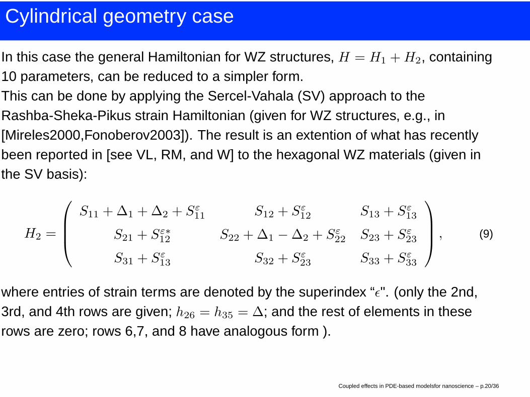
Cylindrical geometry case
In this case the general Hamiltonian for WZ structures, H = H1 +H2, containing10 parameters, can be reduced to a simpler form.This can be done by applying the Sercel-Vahala (SV) approach to theRashba-Sheka-Pikus strain Hamiltonian (given for WZ structures, e.g., in[Mireles2000,Fonoberov2003]). The result is an extention of what has recentlybeen reported in [see VL, RM, and W] to the hexagonal WZ materials (given inthe SV basis):
H2 =
S11 +∆1 +∆2 + Sε
11S12 + Sε
12S13 + Sε
13
S21 + Sε∗
12S22 +∆1 −∆2 + Sε
22S23 + Sε
23
S31 + Sε
13S32 + Sε
23S33 + Sε
33
, (9)
where entries of strain terms are denoted by the superindex “ǫ". (only the 2nd,3rd, and 4th rows are given; h26 = h35 = ∆; and the rest of elements in theserows are zero; rows 6,7, and 8 have analogous form ).
Coupled effects in PDE-based modelsfor nanoscience – p.20/36

Cylindrical geometry case
Operators Sij are second order differential operatorsobtained in a way similar to that described in [VLMW2004], for example
S22 = −~2
2m0
1
2
{
∂
∂ρ
(
(L1 +M1)∂
∂ρ
)
+(L1 +M1)
ρ
∂
∂ρ+
2∂
∂zM2
∂
∂z+
(Fz − J2)
ρ
∂
∂ρ(N1 −N ′
1)−
(Fz − J2)2
ρ2(L1 +M1)
}
, (10)
Based on such a reduced Hamiltonian it is convenientto model rods, cylindrical nanowires and superlattices.
Coupled effects in PDE-based modelsfor nanoscience – p.21/36

Coupling Physical Effects in Modelling QDs: I
Step 1. In order to compute properties of such quantum dot arrays, first wereduce the Maxwell equation to
∇(ǫ∇ϕ) = −ρ+∇ · (P s + P p) (11)
and solve it with equilibrium equations by using the finite element methodology:
∂σxx∂x
+∂σxy∂y
+∂σxz∂z
= 0, (12)
∂σxy∂x
+∂σyy∂y
+∂σyz∂z
= 0, (13)
∂σxz∂x
+∂σyz∂y
+∂σzz∂z
= 0. (14)
These equations are coupled by constitutive equations. In the above equationsP s and P p are spontaneous and strain-induced polarization, respectively.
Coupled effects in PDE-based modelsfor nanoscience – p.22/36

Coupling Physical Effects in Modelling QDs: II
Step 2. The outputs from this model allow us to definethe Hamiltonian of system (2) on the samecomputational grid.
Step 3. By solving the remaining eight coupled ellipticPDEs (1), we find both eigenfunctions and energiescorresponding to all subbands under consideration.
The procedure should be extended if we need toaccount for the carrier density and charge, in whichcase an additional coupling loop is necessary betweenSchrodinger and Poisson parts of the model.
Coupled effects in PDE-based modelsfor nanoscience – p.23/36

InAs/GaAs Pyramidal Quantum Dot: Model Verification
(Ref. Grundmann et al., Phys. Rev. B. 52(16), 11969-11981)
3nm
60nm
30nmY X30nm
30nm30nm
Z
Wetting layer
(a) (b)
Figure 2: (a) Geometry of InAs/GaAs Pyramidal quantum dot (b)biaxial strain distribution in the plane y = 0.
Coupled effects in PDE-based modelsfor nanoscience – p.24/36
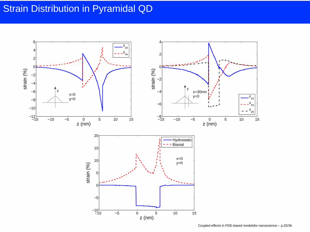
Strain Distribution in Pyramidal QD
−15 −10 −5 0 5 10 15−12
−10
−8
−6
−4
−2
0
2
4
6
z (nm)
stra
in (
%)
εzz
εxx
zx=0y=0
−15 −10 −5 0 5 10 15−8
−6
−4
−2
0
2
4
z (nm)
stra
in (
%)
εzz
εxx
εyy
zx=30nmy=0
−10 −5 0 5 10 15−10
−5
0
5
10
15
20
z (nm)
stra
in (
%)
HydrostaticBiaxial
x=0y=0
Coupled effects in PDE-based modelsfor nanoscience – p.25/36
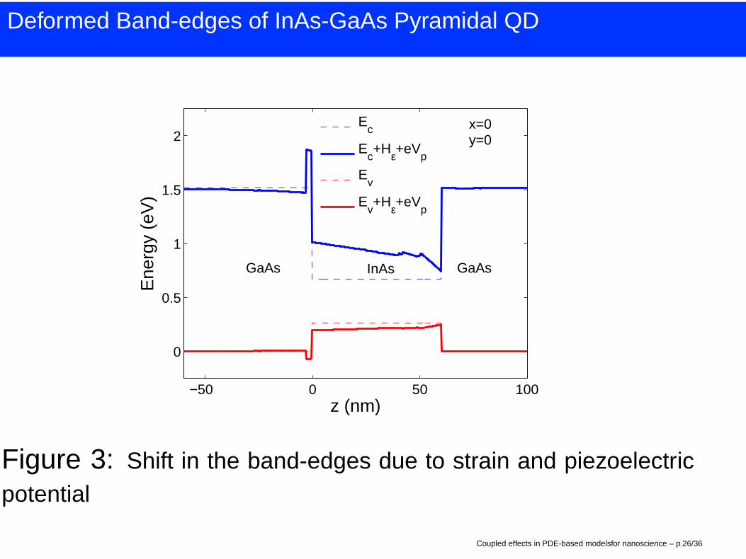
Deformed Band-edges of InAs-GaAs Pyramidal QD
−50 0 50 100
0
0.5
1
1.5
2
z (nm)
Ene
rgy
(eV
)
Ec
Ec+Hε+eV
p
Ev
Ev+Hε+eV
p
GaAs InAs GaAs
x=0y=0
Figure 3: Shift in the band-edges due to strain and piezoelectricpotential
Coupled effects in PDE-based modelsfor nanoscience – p.26/36

Excited states accounting for piezoeffect
Figure 4: Electronic confinement in the quantum dot
Coupled effects in PDE-based modelsfor nanoscience – p.27/36

Deformed Band-edges
−50 0 50 100 150−0.5
0
0.5
1
1.5
2
2.5
z (nm)
Ene
rgy
(eV
)
Ec
Ec+Hε+eV
p
Ev
Ev+Hε+eV
p
x=0y=0
GaAs InAsGaSb GaAs
X
X
Y
Z
InAsGaSb
GaAs
35nm 14nm
180nm
200nm
100nm
80nm
40nm
� Widening of the band-gap due to lattice misfit and piezo effects.
Coupled effects in PDE-based modelsfor nanoscience – p.28/36

Conduction Band Electron Confinement
Figure 5: Confinement for the lowest conduction band energystate with lattice misfit and without piezoelectricity.
Coupled effects in PDE-based modelsfor nanoscience – p.29/36

Effect of Piezoelectricity: Electron states
Ee (eV) (unstrained) Ee (eV) (lattice misfit) Ee (lattice misfit + piezo)
0.4124 0.6332 0.6323
0.4128 0.6339 0.6334
0.4130 0.6345 0.6336
0.4133 0.6364 0.6364
0.4135 0.6485 0.6476
0.4137 0.6486 0.6485
Coupled effects in PDE-based modelsfor nanoscience – p.30/36
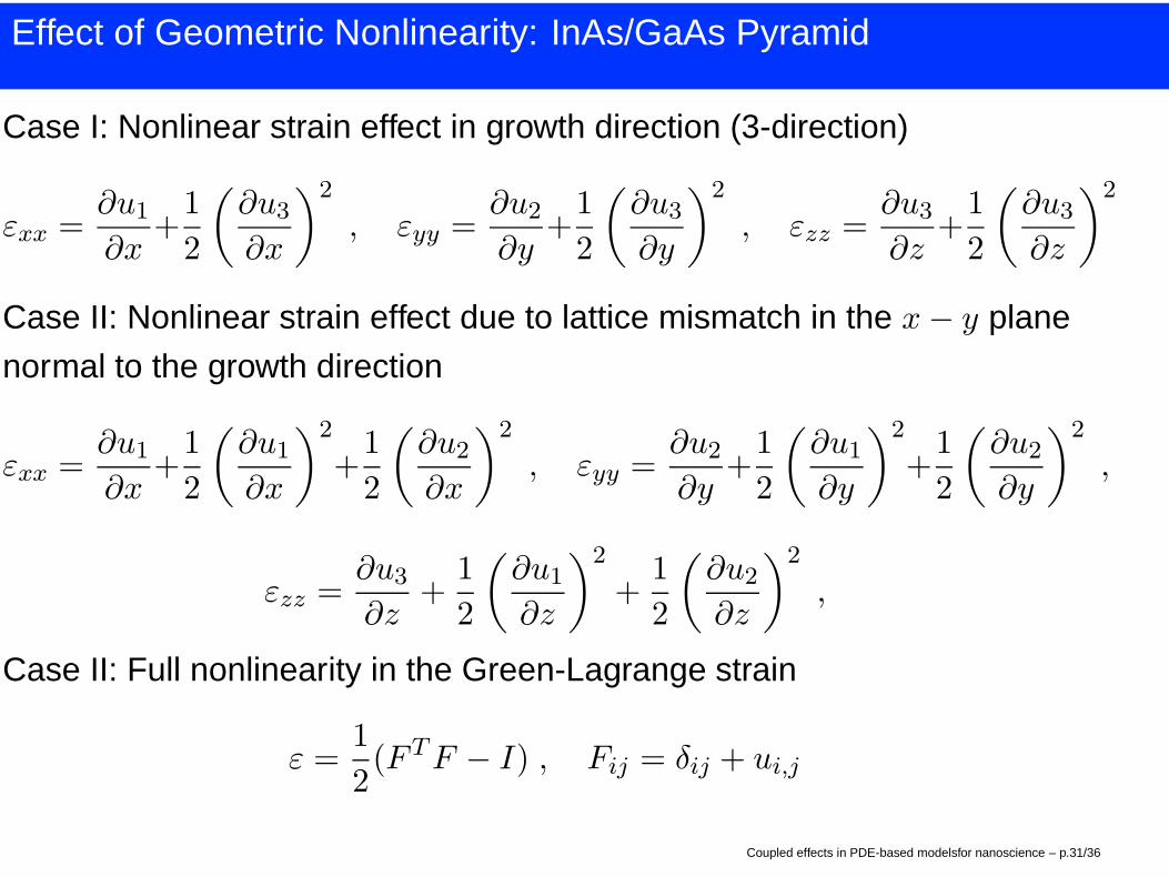
Effect of Geometric Nonlinearity: InAs/GaAs Pyramid
Case I: Nonlinear strain effect in growth direction (3-direction)
εxx =∂u1∂x
+1
2
(
∂u3∂x
)2
, εyy =∂u2∂y
+1
2
(
∂u3∂y
)2
, εzz =∂u3∂z
+1
2
(
∂u3∂z
)2
Case II: Nonlinear strain effect due to lattice mismatch in the x− y plane
normal to the growth direction
εxx =∂u1∂x
+1
2
(
∂u1∂x
)2
+1
2
(
∂u2∂x
)2
, εyy =∂u2∂y
+1
2
(
∂u1∂y
)2
+1
2
(
∂u2∂y
)2
,
εzz =∂u3∂z
+1
2
(
∂u1∂z
)2
+1
2
(
∂u2∂z
)2
,
Case II: Full nonlinearity in the Green-Lagrange strain
ε =1
2(F TF − I) , Fij = δij + ui,j
Coupled effects in PDE-based modelsfor nanoscience – p.31/36
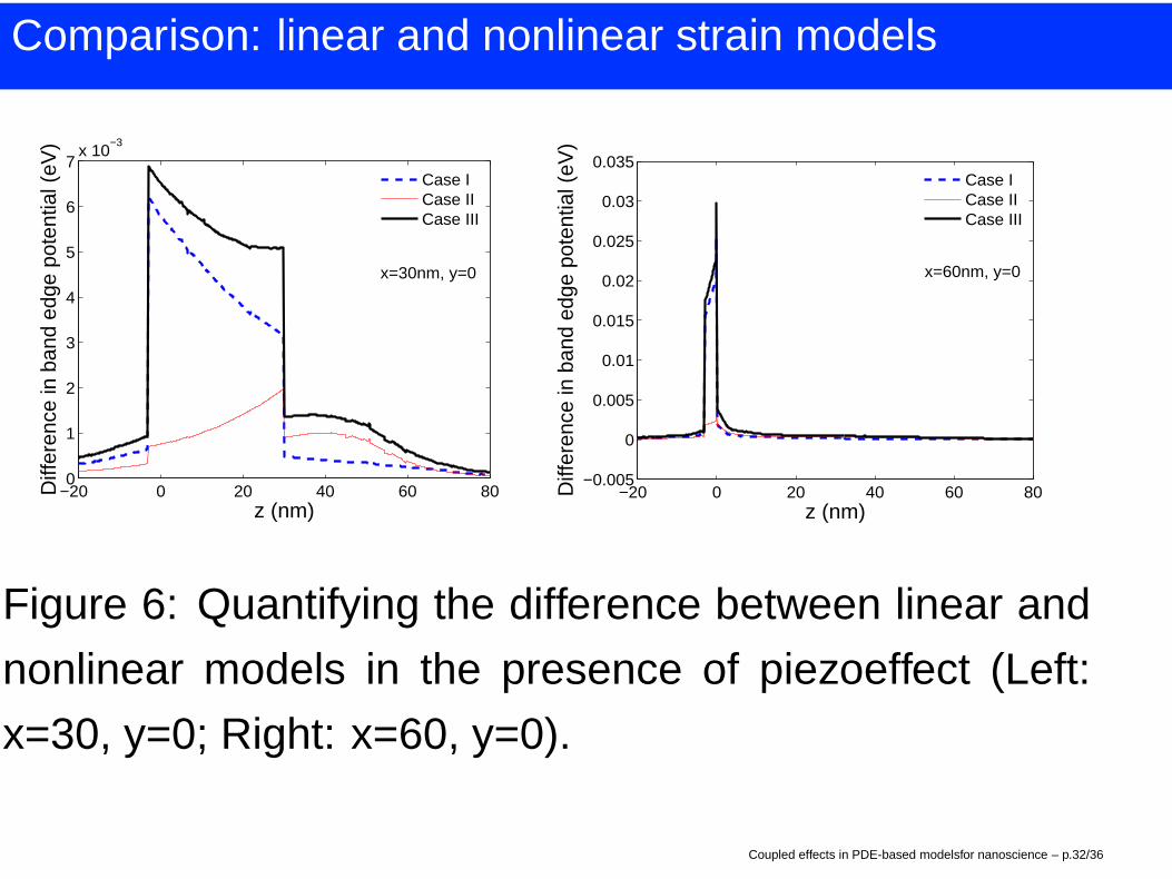
Comparison: linear and nonlinear strain models
−20 0 20 40 60 800
1
2
3
4
5
6
7x 10
−3
z (nm)
Diff
eren
ce in
ban
d ed
ge p
oten
tial (
eV)
Case ICase IICase III
x=30nm, y=0
−20 0 20 40 60 80−0.005
0
0.005
0.01
0.015
0.02
0.025
0.03
0.035
z (nm)
Diff
eren
ce in
ban
d ed
ge p
oten
tial (
eV)
Case ICase IICase III
x=60nm, y=0
Figure 6: Quantifying the difference between linear and
nonlinear models in the presence of piezoeffect (Left:
x=30, y=0; Right: x=60, y=0).
Coupled effects in PDE-based modelsfor nanoscience – p.32/36

Strain, piezo-, and nonlinear contributions
Eigenstate # Lin/strain Lin/strain+piezo Case I Case II Case III
1 0.7122 0.6968 0.6811 0.6913 0.6767
2 0.8345 0.8084 0.8008 0.8070 0.7994
3 0.8404 0.8115 0.8046 0.8095 0.8027
4 0.8511 0.8272 0.8248 0.8267 0.8244
5 0.8658 0.8350 0.8321 0.8345 0.8316
Table 1: The influence of strain, piezoeffects, and non-
linear contributions on eigenstates of the structure.
Coupled effects in PDE-based modelsfor nanoscience – p.33/36
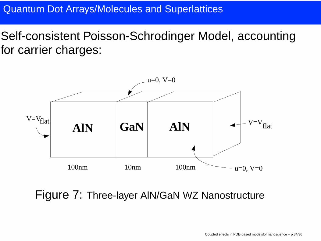
Quantum Dot Arrays/Molecules and Superlattices
Self-consistent Poisson-Schrodinger Model, accountingfor carrier charges:
100nm10nm100nm
AlN GaN AlN
u=0, V=0
V=Vflat
u=0, V=0
flatV=V
Figure 7: Three-layer AlN/GaN WZ Nanostructure
Coupled effects in PDE-based modelsfor nanoscience – p.34/36

Strain and Piezoelectric Potential Distributions
0 50 100 150 200−4
−3
−2
−1
0
1
2
3
4
z (nm)
ε zz (
%)
AlN AlNAlN GaN
0 50 100 150 200−0.4
−0.2
0
0.2
0.4
0.6
0.8
1
1.2
z (nm)
eVp (
eV)
Figure 8: CB electron confinement in strained AlN/GaN WZ QD,Vflat = 1.1eV applied at the AlN edges.
Coupled effects in PDE-based modelsfor nanoscience – p.35/36

Conduction Band Electron Confinement in AlN/GaN QD
Figure 9: States of CB Electron confinement
Coupled effects in PDE-based modelsfor nanoscience – p.36/36

Effect of thermal stresses in quantum dots and wires1,2,3,4
– Increase in the magnitude of the mechanical stress/strain; Decrease in the electric potential and the electric field
– Significantly higher influence on electro-mechanical properties in wurtzite nanostructures as compared to zinc blend
– Influences of the phase transformations and phase stability in nanostructures
– A significant reduction in electronic state energies due to thermal loadings has been observed.
1Patil S. R. and Melnik R. V. N. Nanotechnology Vol. 20, 125402, 2009.2Patil S. R. and Melnik R. V. N. physica status solidi (a), Vol. 206 960, 2009.3Moreira S G C, Silva E C da, Mansanares A M,Barbosa L C and Cesar C L Appl. Phys. Lett Vol. 91, 021101, 20074Wen B and Melnik R V N Appl. Phys. Lett. Vol. 92, 261911, 2008

Accounting for thermo-piezoelectricity
.
,)(
, ,
,
,2)(
3332211
3333331
22141115
1544
15441211
3333331313
2233131112
1131131211
Θ
Θ
Θ
Θ
Θ
Tzzzyyxx
spzzzzyyxxz
yzxyxyzx
yzxzx
xyzyzxyxy
zzzyyxxzz
zzzyyxxyy
zzzyyxxxx
aEpS
PpEeeD
EeDEeD
Eec
Eeccc
Eeccc
Eeccc
Eeccc
++++=
++∈+++=
∈+=∈+=
−=
−=−=
−−++=
−−++=
−−++=
εβεβεβ
εεε
εε
εσ
εσεσ
βεεεσ
βεεεσ
βεεεσ
Coupling of the balance equations is implemented through constitutive equations, derived using the Helmholtz free energyfunction, accounting for three independent variables, ε, E, and ,for the special case of wurtzite symmetry,
Θ
Here cij, eij and χij are elastic moduli, piezoelectric constants and dielectric constants respectively. Pisp is
the spontaneous polarization, pi and βij are thermo-electric and thermo-mechanical coupling constants, respectively and the ε, and E are strain tensor and electric field, respectively
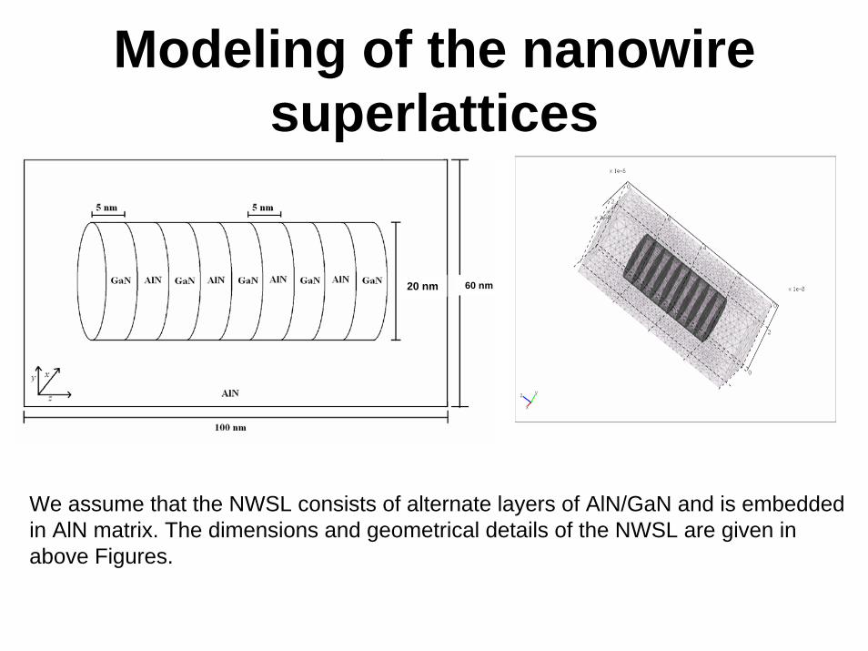
Modeling of the nanowire superlattices
We assume that the NWSL consists of alternate layers of AlN/GaN and is embedded in AlN matrix. The dimensions and geometrical details of the NWSL are given in above Figures.
20 nm 60 nm

Results: Mechanical field distributions I
a) x-component of strain b) y-component of strain c) shear component of strain
The GaN layers are under tensile strain however AlN layers are under compressive strain. The higher magnitudes of the strain-components are along the circumference and across the interfaces between AlN/GaN.

Results: Mechanical field distribution II
The higher (lower) magnitudes of the hydrostatic strains are along the circumference of the GaN(AlN) layers.
Without accounting for thermal stresses the magnitude of hydrostatic strain at the center of the NWSL is 0.019. However, when thermal stresses are accounted for, without external loadings, it increases to 0.0195 and increases even further on external loadings, 0.0205 at 1000K.
Since it is known that hydrostatic strain leads to a rigid shift in the band edges, even small changes caused by thermal stresses become important

Results: Electric field distributions
A giant built-in electric field is observed. Due to this internal electric field, GaN-based LDSNs require relatively higher carrier densities to generate optical gain. Relatively lower carrier densities to generate optical gain may be expected at higher temperatures as our results indicate a decrease in this internal electric field with an increase in temperature.
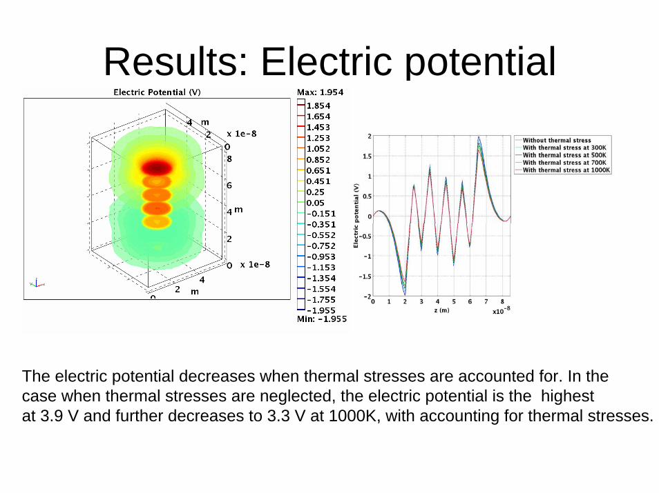
Results: Electric potential
The electric potential decreases when thermal stresses are accounted for. In the case when thermal stresses are neglected, the electric potential is the highest at 3.9 V and further decreases to 3.3 V at 1000K, with accounting for thermal stresses.

Results: Thermal Field distribution
The temperature relaxation is relatively small, however, its effects on electromechanical fieldsandelectronic properties are significant.
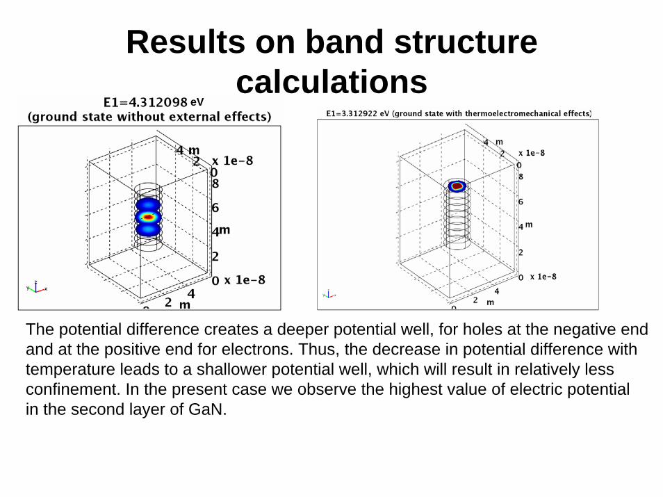
Results on band structure calculations
The potential difference creates a deeper potential well, for holes at the negative end and at the positive end for electrons. Thus, the decrease in potential difference with temperature leads to a shallower potential well, which will result in relatively less confinement. In the present case we observe the highest value of electric potential in the second layer of GaN.
eV

Higher Order Nonlinear Effects in GaN nanostructures
Use Gibbs thermodynamic potential to derive:
Tij = cEijlmSlm − eijnEn + 12c
EijlmpqSlmSpq
−12BijnrEnEr − γijlmnSlmEn
Dk = eklmSlm + ǫSknEn + 12γklmpqSlmSpq
+12ǫ
SknrEnEr +BklmnSlmEn + P sp
(1)
Figure 1: Wetting layer and nonlinear electromechanical field. – p.1/5

Effect of Electrostriction in GaN nanostructures
Figure 2: Wetting layer and nonlinear electromechanical field:electric field
. – p.2/5
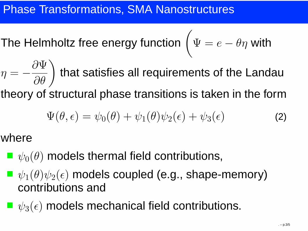
Phase Transformations, SMA Nanostructures
The Helmholtz free energy function(
Ψ = e− θη with
η = −∂Ψ
∂θ
)
that satisfies all requirements of the Landau
theory of structural phase transitions is taken in the form
Ψ(θ, ǫ) = ψ0(θ) + ψ1(θ)ψ2(ǫ) + ψ3(ǫ) (2)
where� ψ0(θ) models thermal field contributions,
� ψ1(θ)ψ2(ǫ) models coupled (e.g., shape-memory)contributions and
� ψ3(ǫ) models mechanical field contributions.. – p.3/5

Coexistence of Different Equilibrium Configurations
−0.2 −0.1 0 0.1 0.2−2780
−2775
−2770
−2765
−2760
Strain
Free
Ene
rgy
(a) Temperature is 200° K
−0.2 −0.1 0 0.1 0.2−3420
−3415
−3410
−3405
−3400
−3395
Strain
Free
Ene
rgy
(b) Temperature is 239° K
−0.2 −0.1 0 0.1 0.2−3522
−3521
−3520
−3519
−3518
−3517
Strain
Free
Ene
rgy
(c) Temperature is 245° K
−0.2 −0.1 0 0.1 0.2−4650
−4640
−4630
−4620
−4610
−4600
−4590
−4580
Strain
Free
Ene
rgy
(d) Temperature is 310° K
Figure 3: Free energy curves for different values of tem-
perature.
. – p.4/5
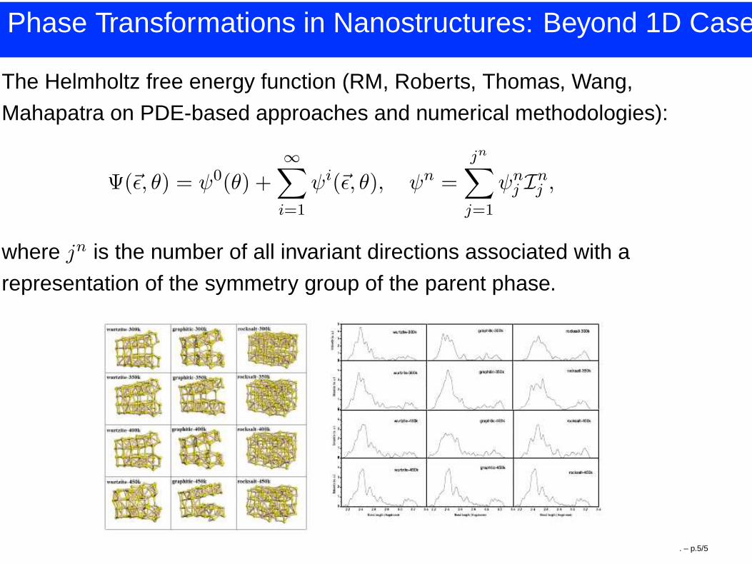
Phase Transformations in Nanostructures: Beyond 1D Case
The Helmholtz free energy function (RM, Roberts, Thomas, Wang,
Mahapatra on PDE-based approaches and numerical methodologies):
Ψ(~ǫ, θ) = ψ0(θ) +
∞∑
i=1
ψi(~ǫ, θ), ψn =
jn∑
j=1
ψnj I
nj ,
where jn is the number of all invariant directions associated with a
representation of the symmetry group of the parent phase.
. – p.5/5
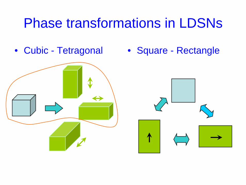
Phase transformations in LDSNs
• Cubic - Tetragonal • Square - Rectangle

For S – R Transformations
Deviatoric strain e2 is chosen the order parameter
At mesoscale :
⎟⎟⎠
⎞⎜⎜⎝
⎛∂∂
−∂∂
=yu
xue 21
2 21
⎟⎠⎞
⎜⎝⎛ −
−−
=c
cbc
cae2
12
aa
c
bb

Governing Equations
11211
21
2
fyxt
u+
∂∂
+∂∂
=∂∂ σσρ 2
221222
2
fyxt
u+
∂∂
+∂∂
=∂∂ σσρ
( )( )
( )( ) .22
2
,21
,22
2
2225
263
24221111
213312
2225
263
24221111
edeaeaeaea
ea
edeaeaeaea
yc
xc
∇+−+−−=
==
∇++−−+=
θθρσ
σρσ
θθρσ

Size Effect - Nanowire
(a)
(b)
(c)
(d)
Evolution of microstructure in FePd nanowire for length 2000 nm, x12 = 0 and width (a) 200 nm (b) 100 nm (c) 95 nm (d) 92 nm
(red and blue indicate martensite variants and green indicates austenite)

Size Effect - Nanowire
• The critical width scale exists below which twin martensite disappears and leads to austenite for the constrained nanowire geometry
• The critical width obtained is 92 nm for FePd nanowire.
• This critical width is higher as compared to uncoupled physics [1]
[1] Bouville, M., and Ahluwalia, R., 2008. “Microstructure and mechanical properties of constrained shape-memory alloy nanograins and nanowires”. Acta Materialia, 56(14), 08, pp. 3558–3567.
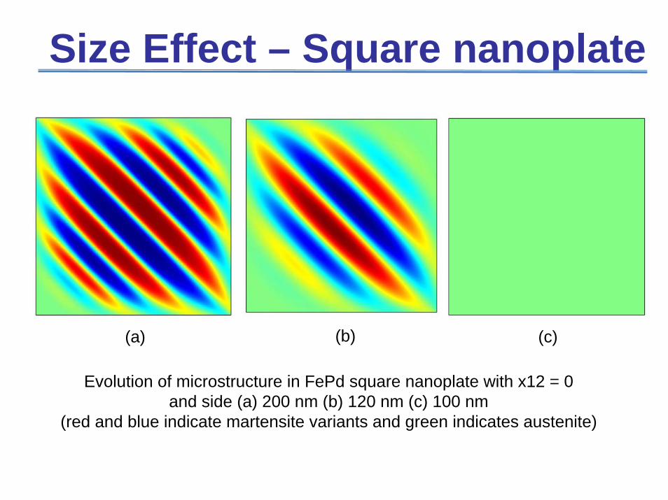
Size Effect – Square nanoplate
Evolution of microstructure in FePd square nanoplate with x12 = 0 and side (a) 200 nm (b) 120 nm (c) 100 nm
(red and blue indicate martensite variants and green indicates austenite)
(a) (b) (c)

Size Effect – Square nanoplate
• The critical size scale also exists below which twin martensite disappears and leads to austenite for the constrained square nanoplate geometry
• The number of twins decreases with decrease in geometry size
• The critical size is 100 nm for FePd square nanoplate.

•Localization of electron wave functions changes significantly from one QD to the other QD or it spreads out into both QDs with the variation of lateral distance between the QDs.
• The distance between the QDs can also provide an additional tuning parameter in the design of QDs-based system.
Coupled QDs and Magnetic Field
M2NeT Laboratoryhttp://www.m2netlab.wlu.ca (6)

Control of electron g-value:The Hamiltonian of the electron spin in presence of external magnetic field which can be added into the Hamiltonian of 8-band into the Bloch sphere which can be written as:
,
1001
3200
0
3000010000100003
340
0010
012
21
⎟⎟⎟⎟⎟⎟⎟⎟⎟⎟⎟
⎠
⎞
⎜⎜⎜⎜⎜⎜⎜⎜⎜⎜⎜
⎝
⎛
⎟⎟⎠
⎞⎜⎜⎝
⎛−
⎟⎟⎟⎟⎟
⎠
⎞
⎜⎜⎜⎜⎜
⎝
⎛
−−
⎟⎟⎠
⎞⎜⎜⎝
⎛−
= zBs BH μ
C. Pryor and M. Flatte, PRL 96, 026804 (2006)
M2NeT Laboratoryhttp://www.m2netlab.wlu.ca (8)
pk ⋅
where 2x2 is the Pauli matrix for spin ½ particle and 4x4 is the Pauli matrix for spin 3/2 particle along z-direction into the Bloch sphere.

E1=4.342221 ev E2=4.37723 ev
•Ground and first excited states of electron spin in AlN/GaN QD.•Found Krammer’s degeneracy in the absence of magnetic field.•Zeeman spin splitting is found at around 0.1 Tesla.
M2NeT Laboratoryhttp://www.m2netlab.wlu.ca (9)
Externally applied magnetic field can be used as a tuning parameter

0.0 0.5 1.0 1.5 2.0 2.5 3.0
4.342124.342164.342204.342244.342284.342324.342364.34240
Ener
gy (e
v)
Magnetic Field (T)
0.0 0.5 1.0 1.5 2.0 2.5 3.0
0.00
0.05
0.10
0.15
0.20
0.25
0.30
Magnetic Field (T)
• The Zeeman energy level splits into two spin-polarized Landau levels.- One with spin parallel to the quantized orbital angular momentum and the
other is antiparallel.• Energy difference of spin splitted ground state increases linearly as a
function of magnetic field.
Spin splitting energy along z-direction
Also see: Wang et al, APL,96, 062108 (2010)
Results cont.
M2NeT Laboratoryhttp://www.m2netlab.wlu.ca (10)
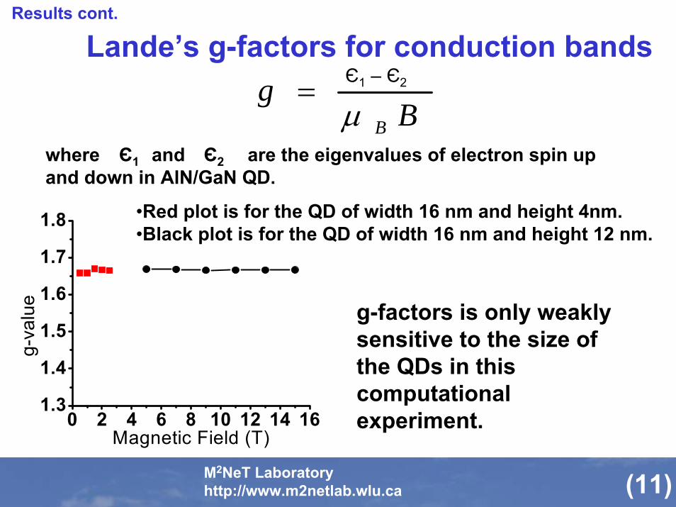
0 2 4 6 8 10 12 14 161.3
1.4
1.5
1.6
1.7
1.8
g-va
lue
Magnetic Field (T)
Lande’s g-factors for conduction bands
Bg
Bμ=
where and are the eigenvalues of electron spin up and down in AlN/GaN QD.
•Red plot is for the QD of width 16 nm and height 4nm.•Black plot is for the QD of width 16 nm and height 12 nm.
g-factors is only weakly sensitive to the size of the QDs in this computational experiment.
Results cont.
Є1 – Є2
Є1 Є2
M2NeT Laboratoryhttp://www.m2netlab.wlu.ca (11)

Modelling biological systems: RNA nanostructures
� Understanding of RNA led to the emergence of the"RNA architectonics" (a set of receipes for(self-)assembly of the RNA nanostructures ofarbitrary size and shape.
� Although better suited for nanoengineeringapplications and medicine, compared to the DNA,the RNA bring a number of additional challenges(one is much larger structural modularity anddiversity of the tertiary structural building blocks, e.g.200 vs 20 for DNA)
� To be successful in developing coarse-grained(mesoscopic) models, it is essential to have inputdata from full molecular dynamics simulations.
. – p.1/5

Getting started
Figure 1: A sample initial configuration from our MD simulations: (RNA hexaring + 165 Mg2+
ions + 88664 H2O). Top and side views of one simulation box (water is not shown).
. – p.2/5

Equilibration and properties
0 50 100 150 200020406080100120140160180200220240260280300320340360380400
0
20
40
60
80
100
120
140
160
180
200
330 Na + 664 NaCl 330 Na + 250 NaCl 330 Na only
N o
f Mg
(out
of 1
65 n
eede
d) a
nd C
l ion
s
N o
f Na
(out
of 3
30 n
eede
d) a
nd C
l ion
s
time, ns*0.01
Na and Mg ions near RNA at T=310K
165 Mg + 250 MgCl2
165 Mg only
0 50 100 150 200020406080100120140160180200220240260280300320340360380400
0
20
40
60
80
100
120
140
160
180
200
330 Na + 664 NaCl 330 Na + 250 NaCl 330 Na only
N o
f Mg
(out
of 1
65 n
eede
d) a
nd C
l ion
s
N o
f Na
(out
of 3
30 n
eede
d) a
nd C
l ion
s
time, ns*0.01
Na and Mg ions near RNA at T=510K
165 Mg + 250 MgCl2
165 Mg only
Figure 2: Number of ions within 5 Å of RNA versus time for two selected temperatures and fora number of concentrations of Na and Mg ions. The colour coding is explained in the body of figures.The scale of the y-axis for Mg2+ ions is set up twice smaller than that for the Na+ ions to allow somebetter visual comparison. The sets of the curves in the lower parts of the plots belong to the Cl ions,whose adsorbtion onto the nanoring is much lower.
. – p.3/5

Stability conditions under quenching
Figure 3: Side and top views of the RNA nanoring in the "physiological solution" of Na (580Na) after 4 ns equilibration at T = 510 K. Bottom snapshot: same for "barely neutralized" system (330Na), it depicts the break of the nanoring in the kissing loop area. Na atoms situated within 5Åof theRNA ring only are shown in green, together with the bound water molecules (red and white). Cl atomsare not shown.
. – p.4/5

New phenomena explanations with a hierarchy of MM
Figure 4: Top views of the RNA nanoring in the barely "neutralized" systems (165 Mg or 330Na) after 1 ns "quenched" equilibration at T = 310 K starting from high temperature configurations.Only those Mg and Na atoms that have been located within 5 Å of RNA nanoring in the beginning ofthe runs are shown (such represnetations allow to visualise the process of the evaporation of the ionsfrom the nanoring). Mg atoms are shown in green, Na atoms are shown in yellow. Waters that havebeen located in the first solvation spheres for Mg and Na in the beginning of the runs are shown in redand white. The phosphorus and two nonbridging oxygens atoms in each phosphate group are showas brown and red spheres. . – p.5/5

Concluding Remarks
� Based on fully coupled models, combinedcontributions of thermo-electromechanical effects tothe electronic properties of LDSNs have beenanalyzed.
� In assisting the design and optimization ofoptoelectronic systems by developing the modelspredicting their properties, it is essential to accountfor the coupled effects that may lead to wellpronounced modifications of QD properties (e.g., atheoretically predicted optical gain is reduced suchthat it can reduce or even prohibit lasing from theground state in some QDs.
. – p.1/4

Concluding Remarks
� Significant reductions and shifts in localizations inelectronic state energies due to thermal loadings areobserved.
� The observed phenomena emphasize theimportance of the fully coupled thermopiezoelectricmodels in studying the properties of LDSNs.
� A key to the validation success is kept at thematerial property level where atomistic details maybe important. This brings an increasing complexitynot only in the moving up to the top of the validationpyramid, but also in the moving to its basis inrevising our mathematical models by accounting fornew important phenomena.
. – p.2/4

Current collaborators on the projects discussed here
� Benny Lassen
� Roy Mahapatra
� Max Paliy
� Bin Wen
� Mehrdad Bahrami-Samani
� Morten Willatzen
� Lok Lew Yan Voon
� Bruce Shapiro
� Sunil Patil
� Sanjay Prabhakar
Support: NSERC, CRC, Sharcnet.. – p.3/4

Thank you
Further details can be found at our group webpage:http://www.m2netlab.wlu.ca
A few recent publications
� Thermoelectromechanical Effects in Quantum Dots, Patil, S. and
Melnik, R.V.N., Nanotechnology, 20, 125402, 2009.
� Molecular dynamics study of the RNA ring nanostructure: a
phenomenon of self-stabilization, Paliy, M., Melnik, R., and Shapiro,
B., Physical Biology, 6(4), 046003, 2009.
� Coarse Graining RNA Nanostructures with Beads, Paliy, M., Melnik,
R., and Shapiro, B., Physical Biology, 7, 036001, 2010.
and more at
http://www.m2netlab.wlu.ca/research/publications-index.html. – p.4/4