Embed Size (px)
Citation preview

Cost-Effective Flash MCU with EEPROM
HT66F302/HT66F303
Revision: V1.30 Date: ana 0 01ana 0 01

Rev. 1.30 ana 0 01 Rev. 1.30 3 ana 0 01
HT66F302/HT66F303Cost-Effective Flash MCU with EEPROM
HT66F302/HT66F303Cost-Effective Flash MCU with EEPROM
Table of Contents
Features ................................................................................................................ 6CPU Feates ..............................................................................................................................6Peipheal Feates ......................................................................................................................6
General Description ............................................................................................. 7Selection Table ..................................................................................................... 7Block Diagram ...................................................................................................... 7Pin Assignment .................................................................................................... 8Pin Description .................................................................................................... 9Absolute Maximum Ratings .............................................................................. 12D.C. Characteristics ........................................................................................... 13A.C. Characteristics ........................................................................................... 14ADC Electrical Characteristics ......................................................................... 15Power on Reset Electrical Characteristics ...................................................... 16System Architecture .......................................................................................... 16
Clocking and Pipelining ..............................................................................................................16Pogam Conte ........................................................................................................................17Stack ..........................................................................................................................................1Aithmetic and Logic Unit – ALU ................................................................................................1
Flash Program Memory ..................................................................................... 19Stcte .....................................................................................................................................19Special Vectos ..........................................................................................................................19Look-p Table .............................................................................................................................19Table Pogam Example .............................................................................................................0In Cicit Pogamming ..............................................................................................................1On-Chip Debg Sppot – OCDS ..............................................................................................1
RAM Data Memory ............................................................................................. 22Stcte .....................................................................................................................................Geneal Ppose Data Memo .................................................................................................Special Ppose Data Memo ..................................................................................................
Special Function Register Description ............................................................ 25Indiect Addessing Registes – IAR0 IAR1 ..............................................................................5Memo Pointes – MP0 MP1 ...................................................................................................5Bank Pointe – BP ......................................................................................................................6Accmlato – ACC ....................................................................................................................6Pogam Conte Low Registe – PCL .......................................................................................6Look-p Table Registes – TBLP TBLH .....................................................................................7Stats Registe – STATUS .........................................................................................................7
Rev. 1.30 ana 0 01 Rev. 1.30 3 ana 0 01
HT66F302/HT66F303Cost-Effective Flash MCU with EEPROM
HT66F302/HT66F303Cost-Effective Flash MCU with EEPROM
EEPROM Data Memory ...................................................................................... 28EEPROM Data Memo Stcte .............................................................................................EEPROM Registes ...................................................................................................................9Reading Data fom the EEPROM .............................................................................................31Witing Data to the EEPROM .....................................................................................................31Wite Potection ..........................................................................................................................31EEPROM Intept .....................................................................................................................31Pogamming Consideations .....................................................................................................3
Oscillators .......................................................................................................... 33Oscillato Oveview ....................................................................................................................33System Clock Configurations .....................................................................................................33Intenal RC Oscillato – HIRC ....................................................................................................34Intenal 3kHz Oscillato – LIRC ................................................................................................34Spplementa Oscillato ...........................................................................................................34
Operating Modes and System Clocks ............................................................. 34Sstem Clocks ...........................................................................................................................34Sstem Opeation Modes ...........................................................................................................35Contol Registe .........................................................................................................................37Opeating Mode Switching ........................................................................................................39Standb Cent Consideations ................................................................................................43Wake-p .....................................................................................................................................43
Watchdog Timer ................................................................................................. 44Watchdog Time Clock Soce ...................................................................................................44Watchdog Time Contol Registe ..............................................................................................44Watchdog Time Opeation ........................................................................................................45
Reset and Initialisation ...................................................................................... 46Reset Fnctions .........................................................................................................................46Reset Initial Conditions ..............................................................................................................50
Input/Output Ports ............................................................................................. 52Pll-high Resistos .....................................................................................................................53Pot A Wake-p ..........................................................................................................................54I/O Pot Contol Registes ..........................................................................................................54Pin-shaed Fnctions .................................................................................................................55Pin-shaed Registes ..................................................................................................................55I/O Pin Stctes .......................................................................................................................57Pogamming Consideations .....................................................................................................5

Rev. 1.30 4 ana 0 01 Rev. 1.30 5 ana 0 01
HT66F302/HT66F303Cost-Effective Flash MCU with EEPROM
HT66F302/HT66F303Cost-Effective Flash MCU with EEPROM
Timer Modules – TM .......................................................................................... 59Intodction ................................................................................................................................59TM Opeation .............................................................................................................................59TM Clock Soce ........................................................................................................................60TM Intepts ..............................................................................................................................60TM Extenal Pins ........................................................................................................................60TM Inpt/Otpt Pin Selection ...................................................................................................61Pogamming Consideations .....................................................................................................6
Standard Type TM – STM .................................................................................. 63Standad TM Opeation ..............................................................................................................63Standad Tpe TM Registe Desciption ....................................................................................63Standad Tpe TM Opeating Modes .........................................................................................6
Periodic Type TM – PTM .................................................................................... 78Peiodic TM Opeation ...............................................................................................................7Peiodic Tpe TM Registe Desciption ......................................................................................7Peiodic Tpe TM Opeating Modes ...........................................................................................3
Analog to Digital Converter – ADC ................................................................... 92A/D Oveview .............................................................................................................................9A/D Convete Registe Desciption ...........................................................................................93A/D Convete Data Registes – SADOL SADOH .....................................................................93A/D Convete Contol Registes – SADC0 SADC1 SADC PASR ........................................93A/D Opeation ............................................................................................................................96A/D Refeence Voltage ...............................................................................................................97A/D Convete Inpt Signal ........................................................................................................9Convesion Rate and Timing Diagam .......................................................................................9Smma of A/D Convesion Steps ............................................................................................99Pogamming Consideations ...................................................................................................100A/D Tansfe Fnction ..............................................................................................................100A/D Pogamming Examples ....................................................................................................101
Interrupts .......................................................................................................... 103Intept Registes ....................................................................................................................103Intept Opeation ...................................................................................................................106Extenal Intept ......................................................................................................................107Mlti-fnction Intept .............................................................................................................10A/D Convete Intept ............................................................................................................10Time Base Intepts ................................................................................................................10EEPROM Intept ...................................................................................................................109TM Intepts ............................................................................................................................ 110 Intept Wake-p Fnction ..................................................................................................... 110Pogamming Consideations ................................................................................................... 110
Configuration Option ....................................................................................... 111Application Circuits ......................................................................................... 111

Rev. 1.30 4 ana 0 01 Rev. 1.30 5 ana 0 01
HT66F302/HT66F303Cost-Effective Flash MCU with EEPROM
HT66F302/HT66F303Cost-Effective Flash MCU with EEPROM
Instruction Set .................................................................................................. 112Intodction .............................................................................................................................. 11Instction Timing ..................................................................................................................... 11Moving and Tansfeing Data .................................................................................................. 11Aithmetic Opeations ............................................................................................................... 11Logical and Rotate Opeation .................................................................................................. 113Banches and Contol Tansfe ................................................................................................ 113Bit Opeations .......................................................................................................................... 113Table Read Opeations ............................................................................................................ 113Othe Opeations ...................................................................................................................... 113
Instruction Set Summary ................................................................................ 114Table Conventions .................................................................................................................... 114
Instruction Definition ....................................................................................... 116Package Information ....................................................................................... 125
-pin SOP (150mil) Otline Dimensions ..................................................................................1610-pin SOP (150mil) Otline Dimensions ................................................................................1716-pin NSOP (150mil) Otline Dimensions ..............................................................................1
Rev. 1.30 6 ana 0 01 Rev. 1.30 7 ana 0 01
HT66F302/HT66F303Cost-Effective Flash MCU with EEPROM
HT66F302/HT66F303Cost-Effective Flash MCU with EEPROM
Features
CPU Features• OperatingVoltage
♦ fSYS=4MHz:1.8V~5.5V♦ fSYS=8MHz:1.8V~5.5V
• Upto0.5μsinstructioncyclewith8MHzsystemclockatVDD=5V
• Powerdownandwake-upfunctionstoreducepowerconsumption
• TwoOscillators♦ InternalRC–HIRC♦ Internal32kHz–LIRC
• Fullyintergratedinternal4/8MHzoscillatorrequiresnoexternalcomponents
• Multi-modeoperation:NORMAL,SLOW,IDLEandSLEEP
• Allinstructionsexecutedinoneortwoinstructioncycles
• Tablereadinstructions
• 63powerfulinstructions
• Upto2-levelsubroutinenesting
• Bitmanipulationinstruction
Peripheral Features• FlashProgramMemory:1K×14
• RAMDataMemory:64×8
• TrueEEPROMMemory:32×8
• WatchdogTimerfunction
• Upto14bidirectionalI/Olines
• Onepin-sharedexternalinterrupt
• MultipleTimerModulesfortimemeasure,comparematchoutput,captureinput,PWMoutput,singlepulseoutputfunctions
• DualTime-Basefunctionsforgenerationoffixedtimeinterruptsignals
• 4-channel12-bitresolutionA/Dconverter
• Lowvoltageresetfunction
• Packagetypes♦ HT66F303:16-pinNSOP♦ HT66F302:8-pinSOP,10-pinSOP

Rev. 1.30 6 ana 0 01 Rev. 1.30 7 ana 0 01
HT66F302/HT66F303Cost-Effective Flash MCU with EEPROM
HT66F302/HT66F303Cost-Effective Flash MCU with EEPROM
General DescriptionThedevicesareaFlashMemorytype8-bithighperformanceRISCarchitecturemicrocontroller.Offeringusers theconvenienceofFlashMemorymulti-programmingfeatures,Thedevicesalsoincludesawiderangeoffunctionsandfeatures.Othermemory includesanareaofRAMDataMemoryaswellasanareaoftrueEEPROMmemoryforstorageofnon-volatiledatasuchasserialnumbers,calibrationdataetc.
Analogfeatures includeamulti-channel12-bitA/Dconverterfunction.MultipleandextremelyflexibleTimerModulesprovidetiming,pulsegeneration,captureinput,comparematchoutputandPWMgenerationfunctions.ProtectivefeaturessuchasaninternalWatchdogTimer,LowVoltageResetcoupledwithexcellentnoiseimmunityandESDprotectionensurethatreliableoperationismaintainedinhostileelectricalenvironments.
Afullchoiceof internaloscillator functionsareprovided includinga fully integratedsystemoscillatorwhichrequiresnoexternalcomponentsforitsimplementation.
TheinclusionofflexibleI/Oprogrammingfeatures,Time-Basefunctionsalongwithmanyotherfeaturesensurethatthedeviceswillfindexcellentuseinapplicationssuchaselectronicmetering,environmentalmonitoring,handheldinstruments,householdappliances,electronicallycontrolledtools,motordrivinginadditiontomanyothers.
Selection TableMostfeaturesarecommontoalldevices.ThemainfeaturesdistinguishingthemareI/Ocountandpackagetypes.Thefollowingtablesummarisesthemainfeaturesofeachdevice.
Part No. Program Memory
Data Memory
Data EEPROM I/O A/D Timer
ModuleTime Base Stack Package
HT66F30 1K×14 64× 3× 1-bit×4 10-bit STM×110-bit PTM×1 /10SOP
HT66F303 1K×14 64× 3× 14 1-bit×4 10-bit STM×110-bit PTM×1 16NSOP
Block Diagram
8-bitRISCMCUCore
I/O
TimeBases
Low Voltage Reset
InterruptController
ResetCircuit
12-bit A/DConverter
RAM Data Memory
TimerModules
WatchdogTimer
Internal RCOscillators
Flash Program Memory
EEPROMData
Memory
Flash/EEPROM Programming Circuitry

Rev. 1.30 ana 0 01 Rev. 1.30 9 ana 0 01
HT66F302/HT66F303Cost-Effective Flash MCU with EEPROM
HT66F302/HT66F303Cost-Effective Flash MCU with EEPROM
Pin Assignment
HT66F3028 SOP-A
VDD/AVDD VSS/AVSSPA7/[PTCK]/[STPB]/RES
PA6/[PTCK]/STPI/[STP]PA5/[INT]/PTPI
PA0/[STPI]/AN0/ICPDAPA1/AN1/VREFIPA2/[INT]/[STCK]/AN2/ICPCK
1234
8765
HT66F30210 SOP-A
VDD/AVDD VSS/AVSS
PA6/[PTCK]/STPI/[STP]PA5/[INT]/PTPI
PA4/[INT]/PTCK/STP
PA0/[STPI]/AN0/ICPDAPA1/AN1/VREFIPA2/[INT]/[STCK]/AN2/ICPCKPA3/INT/STCK/AN3
109876
12345
PA7/[PTCK]/[STPB]/RES
HT66V30216 NSOP-A
VDD/AVDD VSS/AVSS
NCNC
OCDSCK
NCNCOCDSDA
PA7/[PTCK]/[STPB]/RESPA6/[PTCK]/STPI/[STP]
PA5/[INT]/PTPIPA4/[INT]/PTCK/STP
PA0/[STPI]/AN0/ICPDAPA1/AN1/VREFIPA2/[INT]/[STCK]/AN2/ICPCKPA3/INT/STCK/AN3
161514131211109
12345678
HT66F303/HT66V30316 NSOP-A
VSS/AVSSPA0/[STPI]/AN0/OCDSDA/ICPDA
PA1/AN1/VREFIPA2/[INT]/[STCK]/AN2/OCDSCK/ICPCK
PA3/INT/STCK/AN3
VDD/AVDD
PA6/[PTCK]/STPI/[STP]PA5/[INT]/PTPI
PA7/[PTCK]/[STPB]/RES
PA4/[INT]/PTCK/STP
PB2/PTPBPB1/[PTCK]/STPB
PB0/[PTPI]/VREFO
PB3/[PTP]
PB4/[PTPB]PB5/PTP
161514131211109
12345678
Note:1.Bracketedpinnamesindicatenon-defaultpinoutremappinglocations.2.Ifthepin-sharedpinfunctionshavemultipleoutputssimultaneously,thedesiredpin-sharedfunctionisdeterminedbythecorrespondingsoftwarecontrolbits.
3.AVDD&VDDmeans theVDDandAVDDare thedoublebonding.VSS&AVSSmeans theVSSandAVSSarethedoublebonding.
4.TheOCDSDAandOCDSCKpinsaretheOCDSdedicatedpins.TheHT66V303istheEVchipforthe16-pinNSOPpackagedevice,whiletheHT66V302istheEVchipforthe8-pinSOPand10-pinSOPpackagedevice.
5.Animportantpointtonoteisthattheportcontrolbitdenotedas“Dn”inthePBCregisterforHT66F302shouldbeclearedto“0”tosetthecorrespondingpinasanoutputafterpower-onreset.Thiscanpreventthedevicefromconsumingpowerduetoinputfloatingstatesforanyunbondedpins.

Rev. 1.30 ana 0 01 Rev. 1.30 9 ana 0 01
HT66F302/HT66F303Cost-Effective Flash MCU with EEPROM
HT66F302/HT66F303Cost-Effective Flash MCU with EEPROM
Pin DescriptionWiththeexceptionof thepowerpinsandsomerelevant transformercontrolpins,allpinsonthedevicecanbe referencedby theirPortname,e.g.PA0,PA1etc,whichrefer to thedigital I/Ofunctionofthepins.HoweverthesePortpinsarealsosharedwithotherfunctionsuchastheAnalogtoDigitalConverter,TimerModulepinsetc.Thefunctionofeachpinislistedinthefollowingtable,howeverthedetailsbehindhoweachpinisconfigurediscontainedinothersectionsofthedatasheet.
HT66F302Pin Name Function OPT I/T O/T Description
PA0/[STPI]/ AN0/ICPDA
PA0PAWUPAPUPASR
ST CMOS Geneal ppose I/O. Registe enabled pll-high and wake-p.
STPI PASRIFS0 ST — STM inpt
AN0 PASR AN — ADC inpt channel 0 ICPDA — ST CMOS ICP Addess/Data
PA1/AN1/VREFIPA1
PAWUPAPUPASR
ST CMOS Geneal ppose I/O. Registe enabled pll-high and wake-p.
AN1 PASR AN — ADC inpt channel 1 VREFI PASR AN — ADC VREF Inpt
PA/[INT]/[STCK]/ AN/ICPCK
PAPAWUPAPUPASR
ST CMOS Geneal ppose I/O. Registe enabled pll-high and wake-p
INT PASRIFS0 ST — Extenal intept inpt
STCK IFS0 ST — STM clock inptAN PASR AN — ADC inpt channel
ICPCK — ST — ICP Clock pin
PA3/INT/STCK/AN3
PA3PAWUPAPUPASR
ST CMOS Geneal ppose I/O. Registe enabled pll-high and wake-p.
INT PASRIFS0 ST — Extenal intept inpt
STCK IFS0 ST — STM clock inptAN3 PASR AN — ADC inpt channel 3
PA4/[INT]/PTCK/STP
PA4PAWUPAPUPASR
ST CMOS Geneal ppose I/O. Registe enabled pll-high and wake-p.
INT PASRIFS0 ST — Extenal intept inpt
PTCK PASRIFS0 ST — PTM clock inpt
STP PASR — CMOS STM otpt
PA5/[INT]/PTPIPA5 PAWU
PAPU ST CMOS Geneal ppose I/O. Registe enabled pll-high and wake-p.
INT IFS0 ST — Extenal intept inptPTPI IFS0 ST — PTM inpt

Rev. 1.30 10 ana 0 01 Rev. 1.30 11 ana 0 01
HT66F302/HT66F303Cost-Effective Flash MCU with EEPROM
HT66F302/HT66F303Cost-Effective Flash MCU with EEPROM
Pin Name Function OPT I/T O/T Description
PA6/[PTCK]/STPI/[STP]
PA6PAWUPAPUPASR
ST CMOS Geneal ppose I/O. Registe enabled pll-high and wake-p.
PTCK PASRIFS0 ST — PTM clock inpt
STPI PASRIFS0 ST — STM inpt
STP PASR — CMOS STM otpt
PA7/[PTCK]/[STPB]/RES
PA7PAWUPAPUPASR
ST CMOS Geneal ppose I/O. Registe enabled pll-high and wake-p.
PTCK PASRIFS0 — — PTM clock inpt
STPB PASR ST CMOS STM inveting otptRES RSTC ST — Extenal eset inpt
VDD VDD — PWR — Digital positive powe spplAVDD AVDD — PWR — Analog positive powe spplVSS VSS — PWR — Digital negative powe spplAVSS AVSS — PWR — Analog negative powe spplOCDSDA OCDSDA — ST CMOS OCDS Addess/Data fo EV chip onlOCDSCK OCDSCK — ST — OCDS Clock pin fo EV chip onl
HT66F303
Pin Name Function OPT I/T O/T Description
PA0/[STPI]/AN0/OCDSDA/ICPDA
PA0PAWUPAPUPASR
ST CMOS Geneal ppose I/O. Registe enabled pll-high and wake-p.
STPI PASRIFS0 ST — STM inpt
AN0 PASR AN — ADC inpt channel 0 OCDSDA — ST CMOS OCDS Addess/Data fo EV chip onl
ICPDA — ST CMOS ICP Addess/Data
PA1/AN1/VREFIPA1
PAWUPAPUPASR
ST CMOS Geneal ppose I/O. Registe enabled pll-high and wake-p.
AN1 PASR AN — ADC inpt channel 1 VREFI PASR AN — ADC VREF Inpt
PA/[INT]/[STCK]/AN/OCDSCK/ICPCK
PAPAWUPAPUPASR
ST CMOS Geneal ppose I/O. Registe enabled pll-high and wake-p
INT PASRIFS0 ST — Extenal intept inpt
STCK IFS0 ST — STM clock inptAN PASR AN — ADC inpt channel
OCDSCK — ST — OCDS Clock pin fo EV chip onlICPCK — ST — ICP Clock pin

Rev. 1.30 10 ana 0 01 Rev. 1.30 11 ana 0 01
HT66F302/HT66F303Cost-Effective Flash MCU with EEPROM
HT66F302/HT66F303Cost-Effective Flash MCU with EEPROM
Pin Name Function OPT I/T O/T Description
PA3/INT/STCK/AN3
PA3PAWUPAPUPASR
ST CMOS Geneal ppose I/O. Registe enabled pll-high and wake-p.
INT PASRIFS0 ST — Extenal intept inpt
STCK IFS0 ST — STM clock inptAN3 PASR AN — ADC inpt channel 3
PA4/[INT]/PTCK/STP
PA4PAWUPAPUPASR
ST CMOS Geneal ppose I/O. Registe enabled pll-high and wake-p.
INT PASRIFS0 ST — Extenal intept inpt
PTCK PASRIFS0 ST — PTM clock inpt
STP PASR — CMOS STM otpt
PA5/[INT]/PTPIPA5 PAWU
PAPU ST CMOS Geneal ppose I/O. Registe enabled pll-high and wake-p.
INT IFS0 ST — Extenal intept inptPTPI IFS0 ST — PTM inpt
PA6/[PTCK]/STPI/[STP]
PA6PAWUPAPUPASR
ST CMOS Geneal ppose I/O. Registe enabled pll-high and wake-p.
PTCK PASRIFS0 ST — PTM clock inpt
STPI PASRIFS0 ST — STM inpt
STP PASR — CMOS STM otpt
PA7/[PTCK]/[STPB]/RES
PA7PAWUPAPUPASR
ST CMOS Geneal ppose I/O. Registe enabled pll-high and wake-p.
PTCK PASRIFS0 ST — PTM clock inpt
STPB PASR — CMOS STM inveting otptRES RSTC ST — Extenal eset inpt
PB0/[PTPI]/VREFO
PB0 PBPUPBSR ST CMOS Geneal ppose I/O. Registe enabled pll-high
PTPI PBSRIFS0 ST — PTM inpt
VREFO PBSR — AN ADC efeence voltage otpt
PB1/[PTCK]/STPB
PB1 PBPUPBSR ST CMOS Geneal ppose I/O. Registe enabled pll-high
PTCK PBSRIFS0 — — PTM clock inpt
STPB PBSR ST CMOS STM inveting otpt
PB/PTPBPB PBPU
PBSR ST CMOS Geneal ppose I/O. Registe enabled pll-high
PTPB — ST CMOS PTM inveting otpt
PB3/[PTP]PB3 PBPU
PBSR ST CMOS Geneal ppose I/O. Registe enabled pll-high
PTP PBSR — CMOS PTM otpt
PB4/[PTPB]PB4 PBPU
PBSR ST CMOS Geneal ppose I/O. Registe enabled pll-high
PTPB PBSR — CMOS PTM inveting otpt

Rev. 1.30 1 ana 0 01 Rev. 1.30 13 ana 0 01
HT66F302/HT66F303Cost-Effective Flash MCU with EEPROM
HT66F302/HT66F303Cost-Effective Flash MCU with EEPROM
Pin Name Function OPT I/T O/T Description
PB5/PTPPB5 PBPU
PBSR ST CMOS Geneal ppose I/O. Registe enabled pll-high
PTP PBSR — CMOS PTM otptVDD VDD — PWR — Digital positive powe spplAVDD AVDD — PWR — Analog positive powe spplVSS VSS — PWR — Digital negative powe spplAVSS AVSS — PWR — Analog negative powe sppl
Legend:I/T:Inputtype; O/T:OutputtypeOP:OptionalbyregisteroptionPWR:Power; ST:SchmittTriggerinputCMOS:CMOSoutput; AN:AnalogsignalpinVDDis thedevicepowersupplywhileAVDDis theADCpowersupply.TheAVDDpin isbondedtogetherinternallywithVDD.VSSis thedevicegroundpinwhileAVSSis theADCgroundpin.TheAVSSpin isbondedtogetherinternallywithVSS.AsthePinDescriptionSummarytableappliestothepackagetypewiththemostpins,notalloftheabovelistedpinsmaybepresentonpackagetypeswithsmallernumbersofpins.
Absolute Maximum RatingsSupplyVoltage....................................................................................................VSS-0.3VtoVSS+6.0VInputVoltage......................................................................................................VSS-0.3VtoVDD+0.3VStorageTemperature..................................................................................................... -50°Cto125°COperatingTemperature....................................................................................................-40°Cto85°CIOLTotal........................................................................................................................................80mAIOHTotal....................................................................................................................................... -80mATotalPowerDissipation............................................................................................................500mW
Note:Theseare stress ratingsonly.Stressesexceeding the range specifiedunder“AbsoluteMaximumRatings”maycausesubstantialdamage to thedevice.Functionaloperationofthedevicesatotherconditionsbeyondthose listed in thespecification isnot impliedandprolongedexposuretoextremeconditionsmayaffectdevicereliability.

Rev. 1.30 1 ana 0 01 Rev. 1.30 13 ana 0 01
HT66F302/HT66F303Cost-Effective Flash MCU with EEPROM
HT66F302/HT66F303Cost-Effective Flash MCU with EEPROM
D.C. CharacteristicsTa=5°C
Symbol ParameterTest Conditions
Min. Typ. Max. UnitVDD Conditions
VDD Opeating Voltage (HIRC)— fSYS=fHIRC=4MHz 1. — 5.5 V
fSYS=fHIRC=MHz 1. — 5.5 V
IDD
Opeating Cent (HIRC)
3V No load all peipheals off fSYS=fHIRC=4MHz
— 0.5 1.0 mA5V — 1. 1. mA3V No load all peipheals off
fSYS=fHIRC=MHz— 1.0 .0 mA
5V — .0 3.0 mA
Opeating Cent (LIRC)3V No load all peipheals off
fSYS=fLIRC=3kHz— 0 30 μA
5V — 30 60 μA
ISTB
SLEEP0 Mode Standb Cent3V No load all peipheals off
WDT off— 0. 0. μA
5V — 0.5 1.0 μA
SLEEP1 Mode Standb Cent3V No load all peipheals off
WDT on— 1.3 5.0 μA
5V — . 10.0 μA
IDLE0 Mode Standb Cent3V No load all peipheals off
fSUB on— 1.3 3 μA
5V — 5 10 μA
IDLE1 Mode Standb Cent
3V No load all peipheals off fSUB on fSYS=fHIRC=4MHz
— 0.4 0. mA5V — 0.5 1.0 mA3V No load all peipheals off
fSUB on fSYS=fHIRC=MHz— 0. 1.6 mA
5V — 1.0 .0 mAVLVR Low Voltage Reset Voltage — LVR enable voltage select 1.7V - 5% 1.7 + 5% VVBG Bandgap Refeence Voltage 3V — -5% 1.0 +5% V
ILVR Additional Cent fo LVR Enable3V
LVR disable → LVR enable— 6
μA5V — 10 15
VIL
Inpt Low Voltage fo I/O Pots o Inpt Pins except RES Pin
5V — 0 — 1.5 V— — 0 — 0.VDD V
Inpt Low Voltage fo RES Pin — — 0 — 0.4VDD V
VIH
Inpt High Voltage fo I/O Pots o Inpt Pins except RES Pin
5V — 3.5 — 5 V— — 0.VDD — VDD V
Inpt High Voltage fo RES Pin — — 0.9VDD — VDD V
IOL I/O Pot Sink Cent1.V VOL=0.1VDD 7 14 mA3V VOL=0.1VDD 1 36 mA5V VOL=0.1VDD 40 0 mA
IOH I/O Pot Soce Cent3V VOH=0.9VDD -3 -6 mA5V VOH=0.9VDD -7 -14 mA
RPH Pll-high Resistance fo I/O Pots
3V LVPU=0 0 60 100 kΩ5V LVPU=0 10 30 50 kΩ3V LVPU=1 6.67 15 3 kΩ5V LVPU=1 3.5 7.5 1 kΩ

Rev. 1.30 14 ana 0 01 Rev. 1.30 15 ana 0 01
HT66F302/HT66F303Cost-Effective Flash MCU with EEPROM
HT66F302/HT66F303Cost-Effective Flash MCU with EEPROM
A.C. CharacteristicsTa=5°C
Symbol ParameterTest Conditions
Min. Typ. Max. UnitVDD Conditions
fSYSSstem Clock (HIRC)
1.V~5.5V — — 4 — MHz1.V~5.5V — — — MHz
Sstem Clock (LIRC) 1.V~5.5V — — 3 — kHz
fHIRC
4MHz Timmed HIRC Feqenc
3V/5VTa=5°C -1% 4 +1%
MHzTa=-40°C~5°C -% 4 +%
.V~5.5VTa=5°C -.5% 4 +.5%Ta=-40°C~5°C -3% -3%
1.V~5.5V Ta=-40°C~5°C -5% 4 +5%
MHz Timmed HIRC Feqenc
3V/5VTa=5°C -1% +1%
MHzTa=-40°C~5°C -% +%
.V~5.5VTa=5°C -.5% +.5%Ta=-40°C~5°C -3% -3%
1.V~5.5V Ta=-40°C~5°C -5% -5%fLIRC Sstem Clock (LIRC) 1.V~5.5V Ta=-40°C~5°C 3 50 kHztINT Extenal Intept Minimm Plse Width — — 0.3 μstTime xTCK xTPI Inpt Plse Width — — 0.3 μstRES Extenal Reset Low Plse Width — — 10 μstEERD EEPROM Read Time — — 4 tSYS
tEEWR EEPROM Wite Time — — 7.5 ms
tRSTD
Sstem Reset Dela Time(POR Reset LVR Hadwae Reset LVR Softwae Reset WDT Softwae Reset)
— — 5 50 150 ms
Sstem Reset Dela Time(Reset Pin Reset WDT Time-ot Hadwae Cold Reset)
— — .3 16.7 50 ms
tSST
Sstem Stat-p Time Peiod(Wake-p fom HALT fSYS Off at HALT Reset Pin Reset)
— fSYS=fH~fH / 64 fH=fHIRC
16 — — tHIRC
— fSYS=fSUB=fLIRC — — tLIRC
Sstem Stat-p Time Peiod(Wake-p fom HALT fSYS On at HALT State)
— fSYS=fH~fH / 64 fSYS=fHIRC
— — tH
— fSYS=fLIRC — — tSUB
Sstem Stat-p Time Peiod(WDT Time-ot Hadwae Cold Reset) — — 0 — — tH
tBGS VBG Tn on Stable Time — No load — — 150 μstLVR Minimm Low Voltage width to Reset — — 10 600 50 μs
Note:1.tSYS=1/fSYS
2.TomaintaintheaccuracyoftheinternalHIRCoscillatorfrequency,a0.1μFdecouplingcapacitorshouldbeconnectedbetweenVDDandVSSandlocatedasclosetothedeviceaspossible.

Rev. 1.30 14 ana 0 01 Rev. 1.30 15 ana 0 01
HT66F302/HT66F303Cost-Effective Flash MCU with EEPROM
HT66F302/HT66F303Cost-Effective Flash MCU with EEPROM
ADC Electrical CharacteristicsTa=5°C
Symbol ParameterTest Conditions
Min. Typ. Max. UnitVDD Conditions
VDD Opeating Voltage — — 1. — 5.5 VVADI Inpt Voltage — — 0 — VREF VVREF Refeence Voltage — — 1. — VDD V
DNL Diffeential Nonlineait1.V VREF=AVDD=VDD
tADCK=2.0μs-3 — +3 LSB3V VREF=AVDD=VDD
tADCK=0.5μs5V
INL Integal Nonlineait1.V VREF=AVDD=VDD
tADC=.0μs-4 — +4 LSB3V VREF=AVDD=VDD
tADC=0.5μs5V
IADC Additional Cent fo ADC Enable1.V
No load (tADCK=0.5μs)— 0. 1.0 mA
3V — 0. 0.4 mA5V — 0.3 0.6 mA
tADCK Clock Peiod —1.8V ≤ VDD ≤ 2.0V .0 — 10 μs2.0V ≤ VDD ≤ 5.5V 0.5 — 10 μs
tONST ADC on to ADC Stat — — 4 — — μs
tADCConvesion Time(Inclde ADC Sample and Hold Time) — — — 16 — tADCK
IPGA Additional Cent fo PGA Enable1.V No load — 160 50 μA3V No load — 10 300 μA5V No load — 50 350 μA
VCM PGA Common Mode Voltage Range
1.V — 1 — AVDD-0.4 V.V — 1 — AVDD-0.4 V3V — 1 — AVDD-0.4 V5V — 1 — AVDD-0.4 V
VOR PGA Maximm Otpt Voltage Range
1.V — VSS+0.1 — VDD–0.1 V.V — VSS+0.1 — VDD–0.1 V3V — VSS+0.1 — VDD–0.1 V5V — VSS+0.1 — VDD–0.1 V
Ga PGA Gain Accac — — -5 — +5 %

Rev. 1.30 16 ana 0 01 Rev. 1.30 17 ana 0 01
HT66F302/HT66F303Cost-Effective Flash MCU with EEPROM
HT66F302/HT66F303Cost-Effective Flash MCU with EEPROM
Power on Reset Electrical CharacteristicsTa=5°C
Symbol ParameterTest Conditions
Min. Typ. Max. UnitVDD Conditions
VPOR VDD stat voltage to ense powe-on eset — — — — 100 mVRRPOR VDD ising ate to ense powe-on eset — — 0.035 — — V/ms
tPORMinimm time fo VDD stas at VPOR to ense powe-on eset — — 1 — — ms
VDD
tPOR RRPOR
VPORTime
System ArchitectureAkeyfactorinthehigh-performancefeaturesoftheHoltekrangeofmicrocontrollersisattributedtotheirinternalsystemarchitecture.TherangeofdevicestakeadvantageoftheusualfeaturesfoundwithinRISCmicrocontrollersprovidingincreasedspeedofoperationandPeriodicperformance.Thepipeliningschemeisimplementedinsuchawaythatinstructionfetchingandinstructionexecutionareoverlapped,henceinstructionsareeffectivelyexecutedinonecycle,withtheexceptionofbranchorcall instructions.An8-bitwideALUisusedinpracticallyall instructionsetoperations,whichcarriesoutarithmeticoperations,logicoperations,rotation,increment,decrement,branchdecisions,etc.The internaldatapath issimplifiedbymovingdata throughtheAccumulatorandtheALU.Certain internalregistersare implemented in theDataMemoryandcanbedirectlyor indirectlyaddressed.Thesimpleaddressingmethodsof theseregistersalongwithadditionalarchitecturalfeaturesensurethataminimumofexternalcomponentsisrequiredtoprovideafunctionalI/OandA/Dcontrolsystemwithmaximumreliabilityandflexibility.Thismakesthedevicessuitableforlow-cost,high-volumeproductionforcontrollerapplications.
Clocking and PipeliningThemainsystemclock,derivedfromeitheraHIRCorLIRCoscillator issubdivided intofourinternallygeneratednon-overlappingclocks,T1~T4.TheProgramCounter is incrementedat thebeginningoftheT1clockduringwhichtimeanewinstructionisfetched.TheremainingT2~T4clockscarryoutthedecodingandexecutionfunctions.Inthisway,oneT1~T4clockcycleformsoneinstructioncycle.Althoughthefetchingandexecutionofinstructionstakesplaceinconsecutiveinstructioncycles, thepipeliningstructureof themicrocontrollerensures that instructionsareeffectivelyexecuted inone instructioncycle.Theexception to thisare instructionswhere thecontentsoftheProgramCounterarechanged,suchassubroutinecallsorjumps,inwhichcasetheinstructionwilltakeonemoreinstructioncycletoexecute.

Rev. 1.30 16 ana 0 01 Rev. 1.30 17 ana 0 01
HT66F302/HT66F303Cost-Effective Flash MCU with EEPROM
HT66F302/HT66F303Cost-Effective Flash MCU with EEPROM
Fetch Inst. (PC)
(Sstem Clock)fSYS
Phase Clock T1
Phase Clock T
Phase Clock T3
Phase Clock T4
Pogam Conte PC PC+1 PC+
PipeliningExecte Inst. (PC-1) Fetch Inst. (PC+1)
Execte Inst. (PC) Fetch Inst. (PC+)
Execte Inst. (PC+1)
System Clock and Pipelining
For instructions involvingbranches,suchas jumporcall instructions, twomachinecyclesarerequired tocomplete instructionexecution.Anextracycle is requiredas theprogramtakesonecycletofirstobtaintheactualjumporcalladdressandthenanothercycletoactuallyexecutethebranch.Therequirementforthisextracycleshouldbetakenintoaccountbyprogrammersintimingsensitiveapplications.
Fetch Inst. 11 MOV A[1H] CALL DELAY3 CPL [1H]4 :5 :6 DELAY: NOP
Execte Inst. 1 Fetch Inst. Execte Inst.
Fetch Inst. 3 Flsh PipelineFetch Inst. 6 Execte Inst. 6
Fetch Inst. 7
Instruction Fetching
Program CounterDuringprogramexecution, theProgramCounter isused tokeep trackof theaddressof thenext instruction tobeexecuted. It isautomatically incrementedbyoneeach timean instructionisexecutedexcept for instructions, suchas“JMP”or“CALL” thatdemanda jump toanon-consecutiveProgramMemoryaddress.Onlythelower8bits,knownastheProgramCounterLowRegister,aredirectlyaddressablebytheapplicationprogram.
Whenexecuting instructions requiring jumps tonon-consecutiveaddresses suchas a jumpinstruction,asubroutinecall, interruptorreset,etc., themicrocontrollermanagesprogramcontrolbyloadingtherequiredaddressintotheProgramCounter.Forconditionalskipinstructions,oncetheconditionhasbeenmet,thenextinstruction,whichhasalreadybeenfetchedduringthepresentinstructionexecution,isdiscardedandadummycycletakesitsplacewhilethecorrectinstructionisobtained.
Program CounterProgram Counter High byte PCL Register
PC9~PC PCL7~PCL0
The lowerbyteof theProgramCounter,knownas theProgramCounterLowregisterorPCL, isavailableforprogramcontrolandisareadableandwriteableregister.Bytransferringdatadirectlyintothisregister,ashortprogramjumpcanbeexecuteddirectly,however,asonlythis lowbyteisavailableformanipulation,thejumpsarelimitedtothepresentpageofmemory,thatis256locations.Whensuchprogramjumpsareexecuteditshouldalsobenotedthatadummycyclewillbeinserted.ManipulatingthePCLregistermaycauseprogrambranching,soanextracycleisneededtopre-fetch.

Rev. 1.30 1 ana 0 01 Rev. 1.30 19 ana 0 01
HT66F302/HT66F303Cost-Effective Flash MCU with EEPROM
HT66F302/HT66F303Cost-Effective Flash MCU with EEPROM
StackThis isaspecialpartof thememorywhichisusedtosavethecontentsof theProgramCounteronly.Thestackisneitherpartofthedatanorpartoftheprogramspace,andisneitherreadablenorwriteable.TheactivatedlevelisindexedbytheStackPointer,andisneitherreadablenorwriteable.Atasubroutinecallorinterruptacknowledgesignal,thecontentsoftheProgramCounterarepushedontothestack.Attheendofasubroutineoraninterruptroutine,signaledbyareturninstruction,RETorRETI,theProgramCounterisrestoredtoitspreviousvaluefromthestack.Afteradevicereset,theStackPointerwillpointtothetopofthestack.
Ifthestackisfullandanenabledinterrupttakesplace,theinterruptrequestflagwillberecordedbuttheacknowledgesignalwillbeinhibited.WhentheStackPointer isdecremented,byRETorRETI,theinterruptwillbeserviced.Thisfeaturepreventsstackoverflowallowingtheprogrammertousethestructuremoreeasily.However,whenthestackisfull,aCALLsubroutineinstructioncanstillbeexecutedwhichwillresult inastackoverflow.Precautionsshouldbetakentoavoidsuchcaseswhichmightcauseunpredictableprogrambranching.Ifthestackisoverflow,thefirstProgramCountersaveinthestackwillbelost.
Stack Pointe Stack Level
Stack Level 1
Pogam Memo
Pogam Conte
Bottom of Stack
Top of Stack
Arithmetic and Logic Unit – ALUThearithmetic-logicunitorALUisacriticalareaofthemicrocontrollerthatcarriesoutarithmeticandlogicoperationsoftheinstructionset.Connectedtothemainmicrocontrollerdatabus,theALUreceivesrelatedinstructioncodesandperformstherequiredarithmeticor logicaloperationsafterwhichtheresultwillbeplacedinthespecifiedregister.AstheseALUcalculationoroperationsmayresultincarry,borroworotherstatuschanges,thestatusregisterwillbecorrespondinglyupdatedtoreflectthesechanges.TheALUsupportsthefollowingfunctions:
• Arithmeticoperations:ADD,ADDM,ADC,ADCM,SUB,SUBM,SBC,SBCM,DAA
• Logicoperations:AND,OR,XOR,ANDM,ORM,XORM,CPL,CPLA
• Rotation:RRA,RR,RRCA,RRC,RLA,RL,RLCA,RLC
• IncrementandDecrement:INCA,INC,DECA,DEC
• Branchdecision:JMP,SZ,SZA,SNZ,SIZ,SDZ,SIZA,SDZA,CALL,RET,RETI

Rev. 1.30 1 ana 0 01 Rev. 1.30 19 ana 0 01
HT66F302/HT66F303Cost-Effective Flash MCU with EEPROM
HT66F302/HT66F303Cost-Effective Flash MCU with EEPROM
Flash Program MemoryTheProgramMemoryisthelocationwheretheusercodeorprogramisstored.ForthedevicetheProgramMemoryisFlashtype,whichmeansitcanbeprogrammedandre-programmeda largenumberoftimes,allowingtheusertheconvenienceofcodemodificationonthesamedevice.Byusingtheappropriateprogrammingtools,theFlashdeviceoffersuserstheflexibilitytoconvenientlydebuganddevelop their applicationswhilealsoofferingameansof fieldprogrammingandupdating.
StructureTheProgramMemoryhasacapacityof1K×14bits.TheProgramMemoryisaddressedby theProgramCounterandalsocontainsdata,tableinformationandinterruptentries.Tabledata,whichcanbesetupinanylocationwithintheProgramMemory,isaddressedbyaseparatetablepointerregister.
0000H
0004H
03FFH
Reset
Intept Vecto
14 bits
001H
001CH
Program Memory Structure
Special VectorsWithintheProgramMemory,certainlocationsarereservedfortheresetandinterrupts.Thelocation000His reserved foruseby thedevice reset forprograminitialisation.Afteradevice reset isinitiated,theprogramwilljumptothislocationandbeginexecution.
Look-up TableAnylocationwithintheProgramMemorycanbedefinedasalook-uptablewhereprogrammerscanstorefixeddata.Tousethelook-uptable,thetablepointermustfirstbesetupbyplacingtheaddressofthelookupdatatoberetrievedinthetablepointerregister,TBLP.Thisregisterdefinesthetotaladdressofthelook-uptable.
Aftersettingupthetablepointer,thetabledatacanberetrievedfromtheProgramMemoryusingthe“TABRD[m]”or“TABRDL[m]”instructions,respectively.Whentheinstructionisexecuted,the lowerorder tablebyte from theProgramMemorywillbe transferred to theuserdefinedDataMemoryregister[m]asspecified in the instruction.Thehigherorder tabledatabytefromtheProgramMemorywillbe transferred to theTBLHspecial register.Anyunusedbits in thistransferredhigherorderbytewillbereadas“0”.

Rev. 1.30 0 ana 0 01 Rev. 1.30 1 ana 0 01
HT66F302/HT66F303Cost-Effective Flash MCU with EEPROM
HT66F302/HT66F303Cost-Effective Flash MCU with EEPROM
Theaccompanyingdiagramillustratestheaddressingdataflowofthelook-uptable.
Table Program ExampleThefollowingexampleshowshowthetablepointerandtabledataisdefinedandretrievedfromthemicrocontroller.ThisexampleusesrawtabledatalocatedintheProgramMemorywhichisstoredthereusingtheORGstatement.ThevalueatthisORGstatementis“300H”whichreferstothestartaddressofthelastpagewithinthe1KwordsProgramMemoryofthedevice.Thetablepointerissetupheretohaveaninitialvalueof“06H”.ThiswillensurethatthefirstdatareadfromthedatatablewillbeattheProgramMemoryaddress“306H”or6locationsafterthestartofthelastpage.Notethatthevalueforthetablepointerisreferencedtothefirstaddressofthepresentpageifthe“TABRDC[m]”instructionisbeingused.ThehighbyteofthetabledatawhichinthiscaseisequaltozerowillbetransferredtotheTBLHregisterautomaticallywhenthe“TABRDL[m]”instructionisexecuted.
Because theTBLHregister isaread-onlyregisterandcannotberestored,careshouldbe takentoensure itsprotection ifboth themain routineand InterruptServiceRoutineuse table readinstructions. Ifusing the tableread instructions, theInterruptServiceRoutinesmaychange thevalueoftheTBLHandsubsequentlycauseerrorsifusedagainbythemainroutine.Asaruleitisrecommendedthatsimultaneoususeofthetablereadinstructionsshouldbeavoided.However, insituationswheresimultaneoususecannotbeavoided,theinterruptsshouldbedisabledpriortotheexecutionofanymainroutinetable-readinstructions.Notethatalltablerelatedinstructionsrequiretwoinstructioncyclestocompletetheiroperation.
Table Read Program Exampletempreg1 db ? ; temporary register #1tempreg2 db ? ; temporary register #2::mov a,06h ; initialise low table pointer - note that this address mov tblp,a ; is referenced::tabrdl tempreg1 ; transfers value in table referenced by table pointer data at program ; memory address “306H” transferred to tempreg1 and TBLHdec tblp ; reduce value of table pointer by onetabrdl tempreg2 ; transfers value in table referenced by table pointer data at program ; memory address “305H” transferred to tempreg2 and TBLH in this ; example the data “1AH” is transferred to tempreg1 and data “0FH” to ; register tempreg2::org 300h ; sets initial address of program memorydc 00Ah, 00Bh, 00Ch, 00Dh, 00Eh, 00Fh, 01Ah, 01Bh::

Rev. 1.30 0 ana 0 01 Rev. 1.30 1 ana 0 01
HT66F302/HT66F303Cost-Effective Flash MCU with EEPROM
HT66F302/HT66F303Cost-Effective Flash MCU with EEPROM
In Circuit ProgrammingTheprovisionofFlashtypeProgramMemoryprovidestheuserwithameansofconvenientandeasyupgradesandmodifications to theirprogramsonthesamedevice.Asanadditionalconvenience,Holtekhasprovidedameansofprogrammingthemicrocontrollerin-circuitusinga4-pininterface.Thisprovidesmanufacturerswiththepossibilityofmanufacturingtheircircuitboardscompletewithaprogrammedorun-programmedmicrocontroller,andthenprogrammingorupgradingtheprogramata laterstage.Thisenablesproductmanufacturers toeasilykeep theirmanufacturedproductssuppliedwiththelatestprogramreleaseswithoutremovalandre-insertionofthedevice.
Holtek Writer Pins MCU Programming Pins Pin DescriptionICPDA PA0 Pogamming Seial Data/AddessICPCK PA Pogamming ClockVDD VDD Powe SpplVSS VSS Gond
TheProgramMemoryandEEPROMdatamemorycanbothbeprogrammedseriallyin-circuitusingthis4-wireinterface.Dataisdownloadedanduploadedseriallyonasinglepinwithanadditionallinefortheclock.Twoadditionallinesarerequiredforthepowersupplyandground.Thetechnicaldetailsregardingthein-circuitprogrammingofthedevicearebeyondthescopeofthisdocumentandwillbesuppliedinsupplementaryliterature.
* *
Wite_VDD
ICPDA
ICPCK
Wite_VSS
To othe Cicit
VDD
PA0
PA
VSS
Wite Connecto Signals
MCU PogammingPins
Note:*mayberesistororcapacitor.Theresistanceof*mustbegreaterthan1kΩorthecapacitanceof*mustbelessthan1nF.
On-Chip Debug Support – OCDSThere isanEVchipwhich isused toemulate theHT66F302/HT66F303devices.ThisEVchipdevicealsoprovidesan“On-ChipDebug”functiontodebugthedeviceduringthedevelopmentprocess.TheEVchipandtheactualMCUdevicearealmostfunctionallycompatibleexceptforthe“On-ChipDebug”function.UserscanusetheEVchipdevicetoemulatetherealchipdevicebehaviorbyconnectingtheOCDSDAandOCDSCKpinstotheHoltekHT-IDEdevelopmenttools.TheOCDSDApinistheOCDSData/Addressinput/outputpinwhiletheOCDSCKpinistheOCDSclockinputpin.WhenusersusetheEVchipfordebugging,otherfunctionswhicharesharedwiththeOCDSDAandOCDSCKpins in theactualMCUdevicewillhavenoeffect in theEVchip.However,thetwoOCDSpinswhicharepin-sharedwiththeICPprogrammingpinsarestillusedastheFlashMemoryprogrammingpinsforICP.ForamoredetailedOCDSdescription,refertothecorrespondingdocumentnamed“Holteke-Linkfor8-bitMCUOCDSUser’sGuide”.
Holtek e-Link Pins EV Chip Pins Pin DescriptionOCDSDA OCDSDA On-chip Debg Sppot Data/Addess inpt/otptOCDSCK OCDSCK On-chip Debg Sppot Clock inpt
VDD VDD Powe SpplVSS VSS Gond

Rev. 1.30 ana 0 01 Rev. 1.30 3 ana 0 01
HT66F302/HT66F303Cost-Effective Flash MCU with EEPROM
HT66F302/HT66F303Cost-Effective Flash MCU with EEPROM
RAM Data MemoryTheDataMemoryisavolatileareaof8-bitwideRAMinternalmemoryandisthelocationwheretemporaryinformationisstored.
StructureDividedintotwosections,thefirstoftheseisanareaofRAM,knownastheSpecialFunctionDataMemory.Herearelocatedregisterswhicharenecessaryforcorrectoperationofthedevice.Manyoftheseregisterscanbereadfromandwrittentodirectlyunderprogramcontrol,however,someremainprotectedfromusermanipulation.ThesecondareaofDataMemoryisknownastheGeneralPurposeDataMemory,whichisreservedforgeneralpurposeuse.Alllocationswithinthisareaarereadandwriteaccessibleunderprogramcontrol.
TheoverallDataMemoryissubdividedintotwobanks.TheSpecialPurposeDataMemoryregistersareaccessibleinallbanks,withtheexceptionof theEECregisterataddress40H,whichisonlyaccessibleinBank1.SwitchingbetweenthedifferentDataMemorybanksisachievedbysettingtheBankPointertothecorrectvalue.ThestartaddressoftheDataMemoryforthedeviceistheaddress00H.
General Purpose Data MemoryThereis64bytesofgeneralpurposedatamemorywhicharearrangedinBank0.Allmicrocontrollerprogramsrequireanareaofread/writememorywheretemporarydatacanbestoredandretrievedforuselater.ItisthisareaofRAMmemorythatisknownasGeneralPurposeDataMemory.ThisareaofDataMemoryisfullyaccessiblebytheuserprogramingforbothreadingandwritingoperations.Byusingthebitoperation instructions individualbitscanbesetorresetunderprogramcontrolgivingtheuseralargerangeofflexibilityforbitmanipulationintheDataMemory.
Special Purpose Data MemoryThis area ofDataMemory iswhere registers, necessary for the correct operation of themicrocontroller,arestored.Mostof theregistersarebothreadableandwriteablebutsomeareprotectedandarereadableonly,thedetailsofwhicharelocatedundertherelevantSpecialFunctionRegistersection.Notethatforlocationsthatareunused,anyreadinstructiontotheseaddresseswillreturnthevalue“00H”.
Device Capacity Bank 0 Bank 1HT66F30/HT66F303 64× 40H~7FH 40H EEC egiste onl

Rev. 1.30 ana 0 01 Rev. 1.30 3 ana 0 01
HT66F302/HT66F303Cost-Effective Flash MCU with EEPROM
HT66F302/HT66F303Cost-Effective Flash MCU with EEPROM
00H IAR0
01H MP0
02H IAR1
03H MP1
04H
05H ACC
06H PCL
07H TBLP
08H TBLH
09H
INTC1
0AH STATUS
0BH
0CH
0DH
0EH
0FH
10H
SMOD
11H
EEA
12H
19H
18H
1BH
1AH
1DH
1CH
1FH
1EH
13H
14H
15H
16H
17H
INTEG
STMAL
PAPU
PAWU
20H
21H
22H
29H
28H
2BH
2AH
2DH
2CH
2EH
23H
24H
25H
26H
27H
BP
STMDL
STMC1
STMDH
PA
PAC
STMC0
INTC0
: Unused, read as “00”
EED
STMAH
LVPUC
MFI0
IFS0
WDTC
TBC
SMOD1
PASR
RSTC
SADC1
SADC0
SADC2
SADOL
SADOH
Bank 0~1
PTMAH
PTMDH
PTMDL
PTMAL
PTMC1
PTMRPL
33H
32H
35H
34H
37H
36H
38H
2FH
30H
31H
PTMRPH39H
PTMC0
3AH~
3FH
MFI1
Bank 0 Bank 1
LVRC
PBC
: Reserved, cannot be changed unless otherwise specified
Special Purpose Data Memory Structure – HT66F302

Rev. 1.30 4 ana 0 01 Rev. 1.30 5 ana 0 01
HT66F302/HT66F303Cost-Effective Flash MCU with EEPROM
HT66F302/HT66F303Cost-Effective Flash MCU with EEPROM
00H IAR001H MP002H IAR103H MP104H05H ACC06H PCL07H TBLP08H TBLH09H
INTC1
0AH STATUS0BH0CH0DH0EH0FH10H
SMOD
11H
EEA
12H
19H18H
1BH1AH
1DH1CH
1FH1EH
13H14H15H16H17H
INTEGSTMAL
PAPUPAWU
20H21H22H
29H28H
2BH2AH
2DH2CH
2EH
23H24H25H26H27H
BP
STMDLSTMC1
STMDH
PAPAC
STMC0
INTC0
: Unused, read as "00"
EED
STMAHLVPUC
MFI0
IFS0WDTC
TBCSMOD1
PASRRSTC
SADC1SADC0
SADC2
SADOLSADOH
Bank 0~1
PTMAH
PTMDHPTMDL
PTMAL
PTMC1
PTMRPL
PBPUPBCPB
33H32H
35H34H
37H36H
38H
2FH30H31H
PTMRPH39H
PTMC0
3AH~
3FH
MFI1
PBSR
Bank 0 Bank 1
LVRC
Special Purpose Data Memory Structure – HT66F303
Unsed
EEC
GenealPpose
Data Memo
40H
7FH
General Purpose Data Memory

Rev. 1.30 4 ana 0 01 Rev. 1.30 5 ana 0 01
HT66F302/HT66F303Cost-Effective Flash MCU with EEPROM
HT66F302/HT66F303Cost-Effective Flash MCU with EEPROM
Special Function Register DescriptionMostoftheSpecialFunctionRegisterdetailswillbedescribedintherelevantfunctionalsection,howeverseveralregistersrequireaseparatedescriptioninthissection.
Indirect Addressing Registers – IAR0, IAR1TheIndirectAddressingRegisters,IAR0andIAR1,althoughhavingtheirlocationsinnormalRAMregisterspace,donotactuallyphysicallyexistasnormalregisters.ThemethodofindirectaddressingforRAMdatamanipulationuses theseIndirectAddressingRegistersandMemoryPointers, incontrasttodirectmemoryaddressing,wheretheactualmemoryaddressisspecified.ActionsontheIAR0andIAR1registerswillresultinnoactualreadorwriteoperationtotheseregistersbutrathertothememorylocationspecifiedbytheircorrespondingMemoryPointers,MP0orMP1.Actingasapair,IAR0andMP0cantogetheraccessdatafromBank0whiletheIAR1andMP1registerpaircanaccessdatafromanybank.AstheIndirectAddressingRegistersarenotphysicallyimplemented,readingtheIndirectAddressingRegistersindirectlywillreturnaresultof“00H”andwritingtotheregistersindirectlywillresultinnooperation.
Memory Pointers – MP0, MP1TwoMemoryPointers, knownasMP0andMP1areprovided.TheseMemoryPointers arephysicallyimplementedintheDataMemoryandcanbemanipulatedinthesamewayasnormalregistersprovidingaconvenientwaywithwhichtoaddressandtrackdata.WhenanyoperationtotherelevantIndirectAddressingRegistersiscarriedout,theactualaddressthatthemicrocontrollerisdirectedtoistheaddressspecifiedbytherelatedMemoryPointer.MP0,togetherwithIndirectAddressingRegister,IAR0,areusedtoaccessdatafromBank0,whileMP1andIAR1areusedtoaccessdatafromallbanksaccordingtoBPregister.DirectAddressingcanonlybeusedwithBank0,allotherBanksmustbeaddressedindirectlyusingMP1andIAR1.
ThefollowingexampleshowshowtoclearasectionoffourDataMemorylocationsalreadydefinedaslocationsadres1toadres4.
Indirect Addressing Program Exampledata .section ´data´adres1 db ?adres2 db ?adres3 db ?adres4 db ?block db ? code .section at 0 code´org 00hstart: mov a,04h ; setup size of block mov block,a mova,offsetadres1 ;AccumulatorloadedwithfirstRAMaddress movmp0,a ;setupmemorypointerwithfirstRAMaddressloop: clrIAR0 ;clearthedataataddressdefinedbymp0 inc mp0 ; increment memory pointer sdz block ; check if last memory location has been cleared jmp loopcontinue:
Theimportantpointtonotehereisthatintheexampleshownabove,noreferenceismadetospecificDataMemoryaddresses.

Rev. 1.30 6 ana 0 01 Rev. 1.30 7 ana 0 01
HT66F302/HT66F303Cost-Effective Flash MCU with EEPROM
HT66F302/HT66F303Cost-Effective Flash MCU with EEPROM
Bank Pointer – BPFor thedevices, theDataMemory isdivided into twobanks,Bank0andBank1.Selecting therequiredDataMemoryareaisachievedusingtheBankPointer.Bit0oftheBankPointerisusedtoselectDataMemoryBanks0~1.
TheDataMemoryisinitialisedtoBank0afterareset,exceptforaWDTtime-outresetinthePowerDownMode,inwhichcase,theDataMemorybankremainsunaffected.ItshouldbenotedthattheSpecialFunctionDataMemoryisnotaffectedbythebankselection,whichmeansthattheSpecialFunctionRegisterscanbeaccessedfromwithinanybank.DirectlyaddressingtheDataMemorywillalwaysresultinBank0beingaccessedirrespectiveofthevalueoftheBankPointer.AccessingdatafromBank1mustbeimplementedusingIndirectAddressing.
BP Register
Bit 7 6 5 4 3 2 1 0Name — — — — — — — DMBP0R/W — — — — — — — R/WPOR — — — — — — — 0
Bit7~1 Unimplemented,readas“0”Bit0 DMBP0:SelectDataMemoryBanks
0:Bank01:Bank1
Accumulator – ACCTheAccumulator iscentral to theoperationofanymicrocontrollerand isclosely relatedwithoperationscarriedoutby theALU.TheAccumulator is theplacewhereall intermediateresultsfromtheALUarestored.Without theAccumulator itwouldbenecessary towrite theresultofeachcalculationorlogicaloperationsuchasaddition,subtraction,shift,etc., totheDataMemoryresultinginhigherprogrammingandtimingoverheads.Data transferoperationsusually involvethetemporarystoragefunctionoftheAccumulator;forexample,whentransferringdatabetweenoneuser-definedregisterandanother, it isnecessary todo thisbypassing thedata throughtheAccumulatorasnodirecttransferbetweentworegistersispermitted.
Program Counter Low Register – PCLToprovideadditionalprogramcontrolfunctions, the lowbyteof theProgramCounter ismadeaccessibletoprogrammersbylocatingitwithintheSpecialPurposeareaoftheDataMemory.Bymanipulatingthisregister,directjumpstootherprogramlocationsareeasilyimplemented.LoadingavaluedirectlyintothisPCLregisterwillcauseajumptothespecifiedProgramMemorylocation,however,astheregisterisonly8-bitwide,onlyjumpswithinthecurrentProgramMemorypagearepermitted.Whensuchoperationsareused,notethatadummycyclewillbeinserted.

Rev. 1.30 6 ana 0 01 Rev. 1.30 7 ana 0 01
HT66F302/HT66F303Cost-Effective Flash MCU with EEPROM
HT66F302/HT66F303Cost-Effective Flash MCU with EEPROM
Look-up Table Registers – TBLP, TBLHThese twospecial functionregistersareused tocontroloperationof the look-up tablewhich isstoredintheProgramMemory.TBLPisthetablepointerandindicatethelocationwherethetabledata is located. Itsvaluemustbesetupbeforeanytablereadcommandsareexecuted. Itsvaluecanbechanged,forexampleusingthe“INC”or“DEC”instructions,allowingforeasytabledatapointingandreading.TBLHis thelocationwherethehighorderbyteof thetabledata isstoredaftera tablereaddatainstructionhasbeenexecuted.Notethat thelowerordertabledatabyteistransferredtoauserdefinedlocation.
Status Register – STATUSThis8-bitregistercontainsthezeroflag(Z),carryflag(C),auxiliarycarryflag(AC),overflowflag(OV),powerdownflag(PDF),andwatchdogtime-outflag(TO).Thesearithmetic/logicaloperationandsystemmanagementflagsareusedtorecordthestatusandoperationofthemicrocontroller.
WiththeexceptionoftheTOandPDFflags,bitsinthestatusregistercanbealteredbyinstructionslikemostotherregisters.AnydatawrittenintothestatusregisterwillnotchangetheTOorPDFflag.Inaddition,operationsrelatedtothestatusregistermaygivedifferentresultsduetothedifferentinstructionoperations.TheTOflagcanbeaffectedonlybyasystempower-up,aWDTtime-outorbyexecutingthe“CLRWDT”or“HALT”instruction.ThePDFflagisaffectedonlybyexecutingthe“HALT”or“CLRWDT”instructionorduringasystempower-up.
TheZ,OV,ACandCflagsgenerallyreflectthestatusofthelatestoperations.
• Cissetifanoperationresultsinacarryduringanadditionoperationorifaborrowdoesnottakeplaceduringasubtractionoperation;otherwiseCiscleared.Cisalsoaffectedbyarotatethroughcarryinstruction.
• ACissetifanoperationresultsinacarryoutofthelownibblesinaddition,ornoborrowfromthehighnibbleintothelownibbleinsubtraction;otherwiseACiscleared.
• Zissetiftheresultofanarithmeticorlogicaloperationiszero;otherwiseZiscleared.
• OVisset ifanoperationresultsinacarryintothehighest-orderbitbutnotacarryoutofthehighest-orderbit,orviceversa;otherwiseOViscleared.
• PDFisclearedbyasystempower-uporexecutingthe“CLRWDT”instruction.PDFissetbyexecutingthe“HALT”instruction.
• TOisclearedbyasystempower-uporexecutingthe“CLRWDT”or“HALT”instruction.TOissetbyaWDTtime-out.
Inaddition,onenteringaninterruptsequenceorexecutingasubroutinecall,thestatusregisterwillnotbepushedontothestackautomatically.Ifthecontentsofthestatusregistersareimportantandifthesubroutinecancorruptthestatusregister,precautionsmustbetakentocorrectlysaveit.

Rev. 1.30 ana 0 01 Rev. 1.30 9 ana 0 01
HT66F302/HT66F303Cost-Effective Flash MCU with EEPROM
HT66F302/HT66F303Cost-Effective Flash MCU with EEPROM
STATUS Register
Bit 7 6 5 4 3 2 1 0Name — — TO PDF OV Z AC CR/W — — R R R/W R/W R/W R/WPOR — — 0 0 x x x x
"x" nknownBit7~6 Unimplemented,readas“0”Bit5 TO:WatchdogTime-Outflag
0:Afterpoweruporexecutingthe“CLRWDT”or“HALT”instruction1:Awatchdogtime-outoccurred.
Bit4 PDF:Powerdownflag0:Afterpoweruporexecutingthe“CLRWDT”instruction1:Byexecutingthe“HALT”instruction
Bit3 OV:Overflowflag0:Nooverflow1:Anoperationresultsinacarryintothehighest-orderbitbutnotacarryoutofthehighest-orderbitorviceversa.
Bit2 Z:Zeroflag0:Theresultofanarithmeticorlogicaloperationisnotzero1:Theresultofanarithmeticorlogicaloperationiszero
Bit1 AC:Auxiliaryflag0:Noauxiliarycarry1:Anoperationresultsinacarryoutofthelownibblesinaddition,ornoborrowfromthehighnibbleintothelownibbleinsubtraction
Bit0 C:Carryflag0:Nocarry-out1:Anoperationresultsinacarryduringanadditionoperationorifaborrowdoesnottakeplaceduringasubtractionoperation
Cisalsoaffectedbyarotatethroughcarryinstruction.
EEPROM Data MemoryThedevicescontainanareaof internalEEPROMDataMemory.EEPROM,whichstands forElectricallyErasableProgrammableReadOnlyMemory, isby itsnatureanon-volatileformofmemory,withdataretentionevenwhenitspowersupplyisremoved.Byincorporatingthiskindofdatamemory,awholenewhostofapplicationpossibilitiesaremadeavailabletothedesigner.TheavailabilityofEEPROMstorageallowsinformationsuchasproduct identificationnumbers,calibrationvalues,specificuserdata,systemsetupdataorotherproduct informationtobestoreddirectlywithintheproductmicrocontroller.TheprocessofreadingandwritingdatatotheEEPROMmemoryhasbeenreducedtoaverytrivialaffair.
EEPROM Data Memory StructureTheEEPROMDataMemorycapacity is32×8bitsfor thedevices.UnliketheProgramMemoryandRAMDataMemory, theEEPROMDataMemoryisnotdirectlymappedandisthereforenotdirectlyaccessibleinthesamewayastheothertypesofmemory.ReadandWriteoperationstotheEEPROMarecarriedoutinsinglebyteoperationsusingtwoaddressregistersandonedataregisterinBank0andasinglecontrolregisterinBank1.

Rev. 1.30 ana 0 01 Rev. 1.30 9 ana 0 01
HT66F302/HT66F303Cost-Effective Flash MCU with EEPROM
HT66F302/HT66F303Cost-Effective Flash MCU with EEPROM
EEPROM RegistersThreeregisterscontrol theoveralloperationof the internalEEPROMDataMemory.Thesearetheaddressregisters,EEA,thedataregister,EEDandasinglecontrolregister,EEC.AsboththeEEAandEEDregistersarelocatedinallbanks,theycanbedirectlyaccessedinthesamewayasanyotherSpecialFunctionRegister.TheEECregisterhowever,beinglocatedinBank1,cannotbedirectlyaddresseddirectlyandcanonlybereadfromorwrittentoindirectlyusingtheMP1MemoryPointerandIndirectAddressingRegister, IAR1.Because theEECcontrol register is locatedataddress40HinBank1,theMP1MemoryPointermustfirstbesettothevalue40HandtheBankPointerregister,BP,settothevalue,01H,beforeanyoperationsontheEECregisterareexecuted.
RegisterName
Bit
7 6 5 4 3 2 1 0EEA — — — D4 D3 D D1 D0EED D7 D6 D5 D4 D3 D D1 D0EEC — — — — WREN WR RDEN RD
EEPROM Control Registers List
EEA Register
Bit 7 6 5 4 3 2 1 0Name — — — D4 D3 D D1 D0R/W — — — R/W R/W R/W R/W R/WPOR — — — 0 0 0 0 0
Bit7~5 Unimplemented,readas“0”Bit4~0 D4~D0:DataEEPROMaddress
DataEEPROMaddressbit4~bit0
EED Register
Bit 7 6 5 4 3 2 1 0Name D7 D6 D5 D4 D3 D D1 D0R/W R/W R/W R/W R/W R/W R/W R/W R/WPOR 0 0 0 0 0 0 0 0
Bit7~0 D7~D0:DataEEPROMdataDataEEPROMdatabit7~bit0

Rev. 1.30 30 ana 0 01 Rev. 1.30 31 ana 0 01
HT66F302/HT66F303Cost-Effective Flash MCU with EEPROM
HT66F302/HT66F303Cost-Effective Flash MCU with EEPROM
EEC Register
Bit 7 6 5 4 3 2 1 0Name — — — — WREN WR RDEN RDR/W — — — — R/W R/W R/W R/WPOR — — — — 0 0 0 0
Bit7~4 Unimplemented,readas“0”Bit3 WREN:DataEEPROMWriteEnable
0:Disable1:Enable
This is theDataEEPROMWriteEnableBitwhichmustbesethighbeforeDataEEPROMwriteoperationsarecarriedout.Clearingthisbit tozerowill inhibitDataEEPROMwriteoperations.
Bit2 WR:EEPROMWriteControl0:Writecyclehasfinished1:Activateawritecycle
This is theDataEEPROMWriteControlBitandwhensethighbytheapplicationprogramwillactivateawritecycle.Thisbitwillbeautomaticallyresettozerobythehardwareafterthewritecyclehasfinished.SettingthisbithighwillhavenoeffectiftheWRENhasnotfirstbeensethigh.
Bit1 RDEN:DataEEPROMReadEnable0:Disable1:Enable
This is theDataEEPROMReadEnableBitwhichmustbesethighbeforeDataEEPROMreadoperationsarecarriedout.Clearingthisbit tozerowill inhibitDataEEPROMreadoperations.
Bit0 RD:EEPROMReadControl0:Readcyclehasfinished1:Activateareadcycle
This is theDataEEPROMReadControlBitandwhensethighbytheapplicationprogramwillactivateareadcycle.Thisbitwillbeautomaticallyresettozerobythehardwareafterthereadcyclehasfinished.SettingthisbithighwillhavenoeffectiftheRDENhasnotfirstbeensethigh.
Note:TheWREN,WR,RDENandRDcannotbesetto“1”atthesametimeinoneinstruction.TheWRandRDcannotbesetto“1”atthesametime.

Rev. 1.30 30 ana 0 01 Rev. 1.30 31 ana 0 01
HT66F302/HT66F303Cost-Effective Flash MCU with EEPROM
HT66F302/HT66F303Cost-Effective Flash MCU with EEPROM
Reading Data from the EEPROM ToreaddatafromtheEEPROM,thereadenablebit,RDEN,intheEECregistermustfirstbesethightoenablethereadfunction.TheEEPROMaddressofthedatatobereadmustthenbeplacedintheEEAregister.IftheRDbitintheEECregisterisnowsethigh,areadcyclewillbeinitiated.SettingtheRDbithighwillnotinitiateareadoperationif theRDENbithasnotbeenset.Whenthereadcycleterminates,theRDbitwillbeautomaticallyclearedtozero,afterwhichthedatacanbereadfromtheEEDregister.ThedatawillremainintheEEDregisteruntilanotherreadorwriteoperationisexecuted.Theapplicationprogramcanpoll theRDbit todeterminewhenthedataisvalidforreading.
Writing Data to the EEPROMTowritedatatotheEEPROM,theEEPROMaddressofthedatatobewrittenmustfirstbeplacedin theEEAregisterandthedataplacedin theEEDregister.Thenthewriteenablebit,WREN,in theEECregistermustfirstbesethightoenablethewritefunction.After this, theWRbit intheEECregistermustbe immediatelysethigh to initiateawritecycle.These twoinstructionsmustbeexecutedconsecutively.Theglobal interruptbitEMIshouldalsofirstbeclearedbeforeimplementinganywriteoperations,andthensetagainafterthewritecyclehasstarted.Notethatsetting theWRbithighwillnot initiateawritecycle if theWRENbithasnotbeenset.As theEEPROMwritecycle iscontrolledusingan internal timerwhoseoperation isasynchronous tomicrocontrollersystemclock,acertaintimewillelapsebeforethedatawillhavebeenwrittenintotheEEPROM.DetectingwhenthewritecyclehasfinishedcanbeimplementedeitherbypollingtheWRbitintheEECregisterorbyusingtheEEPROMinterrupt.Whenthewritecycleterminates,theWRbitwillbeautomaticallyclearedtozerobythemicrocontroller,informingtheuserthatthedatahasbeenwrittentotheEEPROM.Theapplicationprogramcanthereforepoll theWRbit todeterminewhenthewritecyclehasended.
Write ProtectionProtectionagainst inadvertentwriteoperation isprovided inseveralways.After thedevice ispowered-on theWriteEnablebit in thecontrol registerwillbeclearedpreventinganywriteoperations.Alsoatpower-ontheBankPointer,BP,willbereset tozero,whichmeansthatDataMemoryBank0willbeselected.AstheEEPROMcontrolregisterislocatedinBank1,thisaddsafurthermeasureofprotectionagainstspuriouswriteoperations.Duringnormalprogramoperation,ensuringthattheWriteEnablebitinthecontrolregisterisclearedwillsafeguardagainstincorrectwriteoperations.
EEPROM InterruptTheEEPROMwriteinterruptisgeneratedwhenanEEPROMwritecyclehasended.TheEEPROMinterruptmustfirstbeenabledbysettingtheDEEbit in therelevant interruptregister.WhenanEEPROMwritecycleends,theDEFrequestflagwillbeset.Iftheglobal,EEPROMInterruptareenabledandthestackisnotfull,asubroutinecalltotheEEPROMInterruptvector,willtakeplace.WhentheEEPROMInterruptisserviced,theEEPROMInterruptflagDEFwillbeautomaticallycleared.TheEMIbitwillalsobeautomaticallyclearedtodisableotherinterrupts.
Rev. 1.30 3 ana 0 01 Rev. 1.30 33 ana 0 01
HT66F302/HT66F303Cost-Effective Flash MCU with EEPROM
HT66F302/HT66F303Cost-Effective Flash MCU with EEPROM
Programming ConsiderationsCaremustbetakenthatdataisnotinadvertentlywrittentotheEEPROM.ProtectioncanbePeriodicbyensuringthattheWriteEnablebitisnormallyclearedtozerowhennotwriting.AlsotheBankPointercouldbenormallyclearedtozeroasthiswouldinhibitaccesstoBank1wheretheEEPROMcontrol register exist.Althoughcertainlynotnecessary, considerationmightbegiven in theapplicationprogramtothecheckingofthevalidityofnewwritedatabyasimplereadbackprocess.WhenwritingdatatheWRbitmustbesethighimmediatelyaftertheWRENbithasbeensethigh,toensurethewritecycleexecutescorrectly.Theglobal interruptbitEMIshouldalsobeclearedbeforeawritecycleisexecutedandthenre-enabledafterthewritecyclestarts.Notethatthedeviceshouldnotenter theIDLEorSLEEPmodeuntil theEEPROMreadorwriteoperationis totallycomplete.Otherwise,theEEPROMreadorwriteoperationwillfail.
Programming Examples
Reading data from the EEPROM – polling methodMOVA,EEPROM_ADRES ;userdefinedaddressMOVEEA,AMOVA,040H ;setupmemorypointerMP1MOVMP1,A ;MP1pointstoEECregisterMOVA,01H ;setupBankPointerMOVBP,ASETIAR1.1 ;setRDENbit,enablereadoperationsSETIAR1.0 ;startReadCycle-setRDbitBACK:SZIAR1.0 ;checkforreadcycleendJMPBACKCLRIAR1 ;disableEEPROMwriteCLRBPMOVA,EED ;movereaddatatoregisterMOVREAD_DATA,A
Writing Data to the EEPROM – polling methodMOVA,EEPROM_ADRES ;userdefinedaddressMOVEEA,AMOVA,EEPROM_DATA ;userdefineddataMOVEED,AMOVA,040H ;setupmemorypointerMP1MOVMP1,A ;MP1pointstoEECregisterMOVA,01H ;setupBankPointerMOVBP,ACLREMISETIAR1.3 ;setWRENbit,enablewriteoperationsSETIAR1.2 ;startWriteCycle-setWRbit–executedimmediatelyafter ;setWRENbitSETEMIBACK:SZIAR1.2 ;checkforwritecycleendJMPBACKCLRIAR1 ;disableEEPROMwriteCLRBP

Rev. 1.30 3 ana 0 01 Rev. 1.30 33 ana 0 01
HT66F302/HT66F303Cost-Effective Flash MCU with EEPROM
HT66F302/HT66F303Cost-Effective Flash MCU with EEPROM
OscillatorsVariousoscillatoroptionsoffer theuserawide rangeof functionsaccording to theirvariousapplication requirements.The flexible featuresof theoscillator functionsensure that thebestoptimisationcanbeachievedintermsofspeedandpowersaving.Oscillatorselectionsandoperationareselectedthroughacombinationofconfigurationoptionsandregisters.
Oscillator OverviewInadditiontobeingthesourceofthemainsystemclocktheoscillatorsalsoprovideclocksourcesfortheWatchdogTimerandTimeBaseInterrupts.Twofullyintegratedinternaloscillators,requiringnoexternalcomponents,areprovidedtoformawiderangeofbothfastandslowsystemoscillators.Thehigherfrequencyoscillatorprovideshigherperformancebutcarrywithit thedisadvantageofhigherpowerrequirements,whiletheoppositeisofcoursetrueforthelowerfrequencyoscillator.Withthecapabilityofdynamicallyswitchingbetweenfastandslowsystemclock,thedeviceshavetheflexibility tooptimize theperformance/powerratio,afeatureespecially important inpowersensitiveportableapplications.
Type Name Freq.Intenal High Speed RC HIRC 4 MHzIntenal Low Speed RC LIRC 3kHz
Oscillator Types
System Clock ConfigurationsThereare twomethodsofgeneratingthesystemclock,ahighspeedoscillatoranda lowspeedoscillator.Thehighspeedoscillator is the internal4MHz,8MHzRCoscillator.The lowspeedoscillator is theinternal32kHzRCoscillator.Selectingwhether theloworhighspeedoscillatorisusedasthesystemoscillatorisimplementedusingtheHLCLKbitandCKS2~CKS0bitsintheSMODregisterandasthesystemclockcanbedynamicallyselected.
HIRC PescalefH
LIRC
Low Speed Oscillato
fH/
fH/16
fH/64
fH/
fH/4
fH/3
HLCLKCKS~CKS0 bits
fSYS
fL
High Speed Oscillato
System Clock Configurations

Rev. 1.30 34 ana 0 01 Rev. 1.30 35 ana 0 01
HT66F302/HT66F303Cost-Effective Flash MCU with EEPROM
HT66F302/HT66F303Cost-Effective Flash MCU with EEPROM
Internal RC Oscillator – HIRCTheinternalRCoscillatorisafullyintegratedsystemoscillatorrequiringnoexternalcomponents.TheinternalRCoscillatorhastwofixedfrequencyof4MHz,8MHz.Devicetrimmingduringthemanufacturingprocessandtheinclusionof internalfrequencycompensationcircuitsareusedtoensurethat theinfluenceof thepowersupplyvoltage, temperatureandprocessvariationsontheoscillationfrequencyareminimised.Asaresult,atapowersupplyof5Vandattemperatureof25°Cdegrees,thefixedoscillationfrequencyoftheHIRCwillhaveatolerancewithin1%.
Internal 32kHz Oscillator – LIRCThe internal32kHzSystemOscillator is the lowfrequencyoscillator. It isa fully integratedRCoscillatorwitha typicalfrequencyof32kHzat5V,requiringnoexternalcomponentsfor itsimplementation.Devicetrimmingduringthemanufacturingprocessandtheinclusionof internalfrequencycompensationcircuitsareusedtoensurethattheinfluenceofthepowersupplyvoltage,temperatureandprocessvariationsontheoscillationfrequencyareminimised.
Supplementary OscillatorThelowspeedoscillator, inadditiontoprovidingasystemclocksource isalsousedtoprovideaclocksource to twootherdevicefunctions.Theseare theWatchdogTimerandtheTimeBaseInterrupts.
Operating Modes and System ClocksPresentdayapplicationsrequirethat theirmicrocontrollershavehighperformancebutoftenstilldemandthattheyconsumeaslittlepoweraspossible,conflictingrequirementsthatareespeciallytrueinbatterypoweredportableapplications.Thefastclocksrequiredforhighperformancewillbytheirnatureincreasecurrentconsumptionandofcoursevice-versa, lowerspeedclocksreducecurrentconsumption.AsHoltekhasprovidedthedevicewithbothhighandlowspeedclocksourcesandthemeanstoswitchbetweenthemdynamically, theusercanoptimisetheoperationof theirmicrocontrollertoachievethebestperformance/powerratio.
System ClocksThedeviceshavetwodifferentclocksourcesforboththeCPUandperipheralfunctionoperation.Byprovidingtheuserwithclockoptionsusingregisterprogramming,aclocksystemcanbeconfiguredtoobtainmaximumapplicationperformance.
Themainsystemclock,cancomefromeitherahighfrequency,fH,oralowfrequency,fL,andisselectedusingtheHLCLKbitandCKS2~CKS0bitsintheSMODregister.ThehighspeedsystemclockcanbesourcedfromHIRCoscillator.The lowspeedsystemclocksourcecanbesourcedfromtheinternalclockLIRC.Theotherchoice,whichisadividedversionofthehighspeedsystemoscillatorhasarangeoffH/2~fH/64.
Thereisoneadditionalinternalclockfortheperipheralcircuits, theTimeBaseclock,fTBC.fTBCissourcedfromtheLIRCoscillators.ThefTBCclockisusedasasourcefortheTimeBaseinterruptfunctionsandfortheTMs.

Rev. 1.30 34 ana 0 01 Rev. 1.30 35 ana 0 01
HT66F302/HT66F303Cost-Effective Flash MCU with EEPROM
HT66F302/HT66F303Cost-Effective Flash MCU with EEPROM
HIRC PescalefH
LIRC
Low Speed Oscillato
fH/
fH/16
fH/64
fH/
fH/4
fH/3
HLCLKCKS~CKS0 bits
fSYS
fLIRC
High Speed Oscillato
WDT
fSYS/4
fTBTime Base 0
Time Base 1
TBCK
fL
fTBC
IDLEN
System Clock Configurations
Note:WhenthesystemclocksourcefSYS isswitchedtofLfromfH, thehighspeedoscillationwillstoptoconservethepower.ThusthereisnofH~fH/64forperipheralcircuittouse.
System Operation ModesThere are six differentmodesof operation for themicrocontroller, eachonewith its ownspecial characteristics andwhichcanbe chosenaccording to the specificperformanceandpowerrequirementsof theapplication.Thereare twomodesallowingnormaloperationof themicrocontroller, theNORMALModeandSLOWMode.Theremainingfourmodes,theSLEEP0,SLEEP1, IDLE0andIDLE1modesareusedwhen themicrocontrollerCPUisswitchedoff toconservepower.
Operating ModeDescription
CPU fSYS fLIRC fTBC
NORMAL mode On fH~fH/64 On OnSLOW mode On fL On OnIDLE0 mode Off Off On OnIDLE1 mode Off On On OnSLEEP0 mode Off Off Off OffSLEEP1 mode Off Off On Off

Rev. 1.30 36 ana 0 01 Rev. 1.30 37 ana 0 01
HT66F302/HT66F303Cost-Effective Flash MCU with EEPROM
HT66F302/HT66F303Cost-Effective Flash MCU with EEPROM
NORMAL ModeAsthenamesuggests this isoneof themainoperatingmodeswhere themicrocontrollerhasallofitsfunctionsoperationalandwherethesystemclockisprovidedthehighspeedoscillator.ThismodeoperatesallowingthemicrocontrollertooperatenormallywithaclocksourcewillcomefromthehighspeedoscillatorHIRC.Thehighspeedoscillatorwillhoweverfirstbedividedbyaratiorangingfrom1to64,theactualratiobeingselectedbytheCKS2~CKS0andHLCLKbitsintheSMODregister.Althoughahighspeedoscillatorisused,runningthemicrocontrolleratadividedclockratioreducestheoperatingcurrent.
SLOW ModeThis isalsoamodewhere themicrocontrolleroperatesnormallyalthoughnowwithaslowerspeedclocksource.TheclocksourceusedwillbefromthelowspeedoscillatorLIRC.Runningthemicrocontrollerinthismodeallowsittorunwithmuchloweroperatingcurrents.IntheSLOWMode,thefHisoff.
SLEEP0 ModeTheSLEEPModeisenteredwhenanHALTinstructionisexecutedandwhentheIDLENbitintheSMODregisteris low.IntheSLEEP0modetheCPUwillbestopped,andthefLIRCclockwillbestoppedtoo,andtheWatchdogTimerfunctionisdisabled.
SLEEP1 ModeTheSLEEPModeisenteredwhenanHALTinstructionisexecutedandwhentheIDLENbitintheSMODregisterislow.IntheSLEEP1modetheCPUwillbestopped.HoweverthefLIRCclockswillcontinuetooperateiftheWatchdogTimerfunctionisenabled.
IDLE0 ModeTheIDLE0ModeisenteredwhenaHALTinstructionisexecutedandwhentheIDLENbitintheSMODregisterishighandtheFSYSONbitintheSMOD1registerislow.IntheIDLE0ModethesystemoscillatorwillbeinhibitedfromdrivingtheCPUbutsomeperipheralfunctionswillremainoperationalsuchastheWatchdogTimerandTMs.IntheIDLE0Mode,thesystemoscillatorwillbestopped.
IDLE1 ModeTheIDLE1ModeisenteredwhenaHALTinstructionisexecutedandwhentheIDLENbitintheSMODregisterishighandtheFSYSONbitintheSMOD1registerishigh.IntheIDLE1ModethesystemoscillatorwillbeinhibitedfromdrivingtheCPUbutmaycontinuetoprovideaclocksourcetokeepsomeperipheralfunctionsoperationalsuchastheWatchdogTimerandTMs.IntheIDLE1Mode,thesystemoscillatorwillcontinuetorun,andthissystemoscillatormaybehighspeedorlowspeedsystemoscillator.IntheIDLE1Mode,theWatchdogTimerclock,fLIRC,willbeon.

Rev. 1.30 36 ana 0 01 Rev. 1.30 37 ana 0 01
HT66F302/HT66F303Cost-Effective Flash MCU with EEPROM
HT66F302/HT66F303Cost-Effective Flash MCU with EEPROM
Control RegisterAsingleregister,SMODandSMOD1,isusedforoverallcontroloftheinternalclockswithinthedevice.
SMOD Register
Bit 7 6 5 4 3 2 1 0Name CKS CKS1 CKS0 — LTO HTO IDLEN HLCLKR/W R/W R/W R/W — R R R/W R/WPOR 0 0 0 — 0 0 1 1
Bit7~5 CKS2~CKS0:ThesystemclockselectionwhenHLCLKis“0”000:fL(fLIRC)001:fL(fLIRC)010:fH/64011:fH/32100:fH/16101:fH/8110:fH/4111:fH/2
Thesethreebitsareusedtoselectwhichclockisusedasthesystemclocksource.Inadditiontothesystemclocksource,whichcanbetheLIRC,adividedversionofthehighspeedsystemoscillatorcanalsobechosenasthesystemclocksource.
Bit4 Unimplemented,readas“0”Bit3 LTO:Lowspeedsystemoscillatorreadyflag
0:Notready1:Ready
Thisisthelowspeedsystemoscillatorreadyflagwhichindicateswhenthelowspeedsystemoscillator isstableafterpoweronresetorawake-uphasoccurred.TheflagwillbelowwhenintheSLEEP0mode,butafterawake-uphasoccurredtheflagwillchangetoahighlevelafter1~2cyclesiftheLIRCoscillatorisused.
Bit2 HTO:Highspeedsystemoscillatorreadyflag0:Notready1:Ready
Thisisthehighspeedsystemoscillatorreadyflagwhichindicateswhenthehighspeedsystemoscillatorisstable.Thisflagisclearedto“0”byhardwarewhenthedeviceispoweredonandthenchangestoahighlevelafterthehighspeedsystemoscillatorisstable.Thereforethisflagwillalwaysbereadas“1”bytheapplicationprogramafterdevicepower-on.
Bit1 IDLEN:IDLEModeControl0:Disable1:Enable
This is theIDLEModeControlbitanddetermineswhathappenswhentheHALTinstructionisexecuted.If thisbit ishigh,whenaHALTinstructionisexecutedthedevicewillenter theIDLEMode. In theIDLE1Mode theCPUwillstoprunningbut thesystemclockwillcontinue tokeep theperipheral functionsoperational, ifFSYSONbitishigh.IfFSYSONbitislow,theCPUandthesystemclockwillallstopinIDLE0mode.IfthebitislowthedevicewillentertheSLEEPModewhenaHALTinstructionisexecuted.
Bit0 HLCLK:SystemClockSelection0:fH/2~fH/64orfL1:fH
Thisbit isusedtoselect if thefHclockor thefH/2~fH/64orfLclockisusedas thesystemclock.When thebit ishigh the fH clockwillbe selectedand if low thefH/2~fH/64orfLclockwillbeselected.WhensystemclockswitchesfromthefHclocktothefLclockandthefHclockwillbeautomaticallyswitchedofftoconservepower.

Rev. 1.30 3 ana 0 01 Rev. 1.30 39 ana 0 01
HT66F302/HT66F303Cost-Effective Flash MCU with EEPROM
HT66F302/HT66F303Cost-Effective Flash MCU with EEPROM
SMOD1 Register
Bit 7 6 5 4 3 2 1 0Name FSYSON — — — RSTF LVRF LRF WRFR/W R/W — — — R/W R/W R/W R/WPOR 0 — — — 0 x 0 0
“x” nknownBit7 FSYSON:fSYSControlinIDLEMode
0:Disable1:Enable
Bit6~4 Unimplemented,readas“0”Bit3 RSTF:ResetcausedbyRSTCsetting
0:Notoccurr1:Occurred
Thisbitcanbeclear to“0”,butcannotset to“1”.If thisbit isset,onlyclearedbySoftwareorPORreset.
Bit2 LVRF:LVRfunctionresetflag0:Notoccurr1:Occurred
Thisbit isset to1whenaspecificLowVoltageResetsituationoccurs.Thisbitcanonlybeclearedto0bytheapplicationprogram.
Bit1 LRF:LVRControlregistersoftwareresetflag0:Notoccurr1:Occurred
Thisbitissetto1iftheLVRCregistercontainsanynondefinedLVRvoltageregistervalues.Thisineffectactslikeasoftware-resetfunction.Thisbitcanonlybeclearedto0bytheapplicationprogram.
Bit0 WRF:WDTControlregistersoftwareresetflag0:Notoccur1:Occurred
Thisbit isset to1by theWDTControlregistersoftwareresetandclearedby theapplicationprogram.Note that thisbitcanonlybecleared to0bytheapplication.program.

Rev. 1.30 3 ana 0 01 Rev. 1.30 39 ana 0 01
HT66F302/HT66F303Cost-Effective Flash MCU with EEPROM
HT66F302/HT66F303Cost-Effective Flash MCU with EEPROM
Operating Mode Switching Thedevicecanswitchbetweenoperatingmodesdynamicallyallowingtheusertoselect thebestperformance/powerratiofor thepresent taskinhand.Inthiswaymicrocontrolleroperationsthatdonotrequirehighperformancecanbeexecutedusingslowerclocksthusrequiringlessoperatingcurrentandprolongingbatterylifeinportableapplications.
Insimple terms,ModeSwitchingbetween theNORMALModeandSLOWMode isexecutedusingtheHLCLKbitandCKS2~CKS0bitsintheSMODregisterwhileModeSwitchingfromtheNORMAL/SLOWModestotheSLEEP/IDLEModesisexecutedviatheHALTinstruction.WhenaHALTinstructionisexecuted,whetherthedeviceenterstheIDLEModeortheSLEEPModeisdeterminedbytheconditionoftheIDLENbitintheSMODregisterandFSYSONintheSMOD1register.
WhentheHLCLKbitswitchestoalowlevel,whichimpliesthatclocksourceisswitchedfromthehighspeedclocksource,fH,totheclocksource,fH/2~fH/64orfL.IftheclockisfromthefL,thehighspeedclocksourcewillstoprunningtoconservepower.WhenthishappensitmustbenotedthatthefH/16andfH/64internalclocksourceswillalsostoprunning,whichmayaffecttheoperationofotherinternalfunctionssuchastheTMs.

Rev. 1.30 40 ana 0 01 Rev. 1.30 41 ana 0 01
HT66F302/HT66F303Cost-Effective Flash MCU with EEPROM
HT66F302/HT66F303Cost-Effective Flash MCU with EEPROM
NORMAL Mode to SLOW Mode SwitchingWhenrunningintheNORMALMode,whichusesthehighspeedsystemoscillator,andthereforeconsumesmorepower, thesystemclockcanswitch to run in theSLOWModebysetting theHLCLKbitto“0”andsettingtheCKS2~CKS0bitsto“000”or“001”intheSMODregister.Thiswillthenusethelowspeedsystemoscillatorwhichwillconsumelesspower.Usersmaydecidetodothisforcertainoperationswhichdonotrequirehighperformanceandcansubsequentlyreducepowerconsumption.
TheSLOWModeissourcedfromtheLIRCoscillatorandthereforerequires thisoscillator tobestablebeforefullmodeswitchingoccurs.ThisismonitoredusingtheLTObitintheSMODregister.

Rev. 1.30 40 ana 0 01 Rev. 1.30 41 ana 0 01
HT66F302/HT66F303Cost-Effective Flash MCU with EEPROM
HT66F302/HT66F303Cost-Effective Flash MCU with EEPROM
SLOW Mode to NORMAL Mode Switching InSLOWModethesystemusesLIRClowspeedsystemoscillator.ToswitchbacktotheNORMALMode,where thehighspeedsystemoscillator isused, theHLCLKbit shouldbeset to“1”orHLCLKbit is“0”,butCKS2~CKS0isset to“010”,“011”,“100”,“101”,“110”or“111”.Asacertainamountoftimewillberequiredforthehighfrequencyclocktostabilise,thestatusoftheHTObitischecked.
Entering the SLEEP0 ModeThereisonlyonewayforthedevicetoentertheSLEEP0Modeandthatistoexecutethe“HALT”instructionintheapplicationprogramwiththeIDLENbitinSMODregisterequalto“0”andtheWDToff.Whenthisinstructionisexecutedundertheconditionsdescribedabove,thefollowingwilloccur:
• Thesystemclock,WDTclockandTimeBaseclockwillbestoppedandtheapplicationprogramwillstopatthe“HALT”instruction.
• TheDataMemorycontentsandregisterswillmaintaintheirpresentcondition.
• TheWDTwillbeclearedandstopped.
• TheI/Oportswillmaintaintheirpresentconditions.
• Inthestatusregister,thePowerDownflag,PDF,willbesetandtheWatchdogtime-outflag,TO,willbecleared.

Rev. 1.30 4 ana 0 01 Rev. 1.30 43 ana 0 01
HT66F302/HT66F303Cost-Effective Flash MCU with EEPROM
HT66F302/HT66F303Cost-Effective Flash MCU with EEPROM
Entering the SLEEP1 ModeThereisonlyonewayforthedevicetoentertheSLEEP1Modeandthatistoexecutethe“HALT”instructionintheapplicationprogramwiththeIDLENbitinSMODregisterequalto“0”andtheWDTon.Whenthisinstructionisexecutedundertheconditionsdescribedabove,thefollowingwilloccur:
• ThesystemclockandTimeBaseclockwillbestoppedandtheapplicationprogramwillstopatthe“HALT”instruction,buttheWDTwillremainwiththeclocksourcecomingfromthefLIRCclock.
• TheDataMemorycontentsandregisterswillmaintaintheirpresentcondition.
• TheWDTwillbeclearedandresumecountingiftheWDTisenabled.
• TheI/Oportswillmaintaintheirpresentconditions.
• Inthestatusregister,thePowerDownflag,PDF,willbesetandtheWatchdogtime-outflag,TO,willbecleared.
Entering the IDLE0 ModeThereisonlyonewayforthedevicetoentertheIDLE0Modeandthatistoexecutethe“HALT”instructionintheapplicationprogramwiththeIDLENbitinSMODregisterequalto“1”andtheFSYSONbitinSMOD1registerequalto“0”.Whenthisinstructionisexecutedundertheconditionsdescribedabove,thefollowingwilloccur:
• The systemclockwill be stoppedand the applicationprogramwill stopat the “HALT”instruction,buttheTimeBaseclockwillbeon.
• TheDataMemorycontentsandregisterswillmaintaintheirpresentcondition.
• TheWDTwillbeclearedandresumecountingiftheWDTisenabled.
• TheI/Oportswillmaintaintheirpresentconditions.
• Inthestatusregister,thePowerDownflag,PDF,willbesetandtheWatchdogtime-outflag,TO,willbecleared.
Entering the IDLE1 ModeThereisonlyonewayforthedevicetoentertheIDLE1Modeandthatistoexecutethe“HALT”instructionintheapplicationprogramwiththeIDLENbitinSMODregisterequalto“1”andtheFSYSONbitinSMOD1registerequalto“1”.Whenthisinstructionisexecutedundertheconditionsdescribedabove,thefollowingwilloccur:
• ThesystemclockandTimeBaseclockwillbeonandtheapplicationprogramwillstopatthe“HALT”instruction.
• TheDataMemorycontentsandregisterswillmaintaintheirpresentcondition.
• TheWDTwillbeclearedandresumecountingiftheWDTisenabled.
• TheI/Oportswillmaintaintheirpresentconditions.
• Inthestatusregister,thePowerDownflag,PDF,willbesetandtheWatchdogtime-outflag,TO,willbecleared.

Rev. 1.30 4 ana 0 01 Rev. 1.30 43 ana 0 01
HT66F302/HT66F303Cost-Effective Flash MCU with EEPROM
HT66F302/HT66F303Cost-Effective Flash MCU with EEPROM
Standby Current ConsiderationsAsthemainreasonforenteringtheSLEEPorIDLEModeistokeepthecurrentconsumptionofthedevicetoaslowavalueaspossible,perhapsonlyintheorderofseveralmicro-ampsexceptintheIDLE1Mode,thereareotherconsiderationswhichmustalsobetakenintoaccountbythecircuitdesignerifthepowerconsumptionistobeminimised.SpecialattentionmustbemadetotheI/Opinsonthedevice.Allhigh-impedanceinputpinsmustbeconnectedtoeitherafixedhighorlowlevelasanyfloatinginputpinscouldcreateinternaloscillationsandresultinincreasedcurrentconsumption.Thisalsoappliestothedevicewhichhasdifferentpackagetypes,astheremaybeunbonbedpins.Thesemusteitherbesetupasoutputsorifsetupasinputsmusthavepull-highresistorsconnected.
Caremustalsobe takenwith the loads,whichareconnected to I/Opins,whichare setupasoutputs.Theseshouldbeplacedinaconditioninwhichminimumcurrent isdrawnorconnectedonlytoexternalcircuitsthatdonotdrawcurrent,suchasotherCMOSinputs.IntheIDLE1Modethesystemoscillator ison, if thesystemoscillator is fromthehighspeedsystemoscillator, theadditionalstandbycurrentwillalsobeperhapsintheorderofseveralhundredmicro-amps.
Wake-upAfterthesystementerstheSLEEPorIDLEMode,itcanbewokenupfromoneofvarioussourceslistedasfollows:
• Anexternalreset
• AnexternalfallingedgeonPortA
• Asysteminterrupt
• AWDToverflow
If thesystemiswokenupbyanexternal reset, thedevicewillexperiencea full systemreset,however,IfThedevicesarewokenupbyaWDToverflow,aWatchdogTimerresetwillbeinitiated.Althoughbothof thesewake-upmethodswill initiatearesetoperation, theactualsourceof thewake-upcanbedeterminedbyexaminingtheTOandPDFflags.ThePDFflag isclearedbyasystempower-uporexecutingtheclearWatchdogTimerinstructionsandissetwhenexecutingthe“HALT”instruction.TheTOflagissetifaWDTtime-outoccurs,andcausesawake-upthatonlyresetstheProgramCounterandStackPointer,theotherflagsremainintheiroriginalstatus.
EachpinonPortAcanbesetupusingthePAWUregistertopermitanegativetransitiononthepintowake-upthesystem.WhenaPortApinwake-upoccurs,theprogramwillresumeexecutionattheinstructionfollowingthe“HALT”instruction.If thesystemiswokenupbyaninterrupt, thentwopossiblesituationsmayoccur.Thefirstiswheretherelatedinterruptisdisabledortheinterruptisenabledbutthestackisfull,inwhichcasetheprogramwillresumeexecutionattheinstructionfollowingthe“HALT”instruction.Inthissituation,theinterruptwhichwoke-upthedevicewillnotbeimmediatelyserviced,butwillratherbeservicedlaterwhentherelatedinterruptisfinallyenabledorwhenastacklevelbecomesfree.Theothersituationiswheretherelatedinterruptisenabledandthestackisnotfull,inwhichcasetheregularinterruptresponsetakesplace.Ifaninterruptrequestflag issethighbeforeentering theSLEEPorIDLEMode, thewake-upfunctionof therelatedinterruptwillbedisabled.

Rev. 1.30 44 ana 0 01 Rev. 1.30 45 ana 0 01
HT66F302/HT66F303Cost-Effective Flash MCU with EEPROM
HT66F302/HT66F303Cost-Effective Flash MCU with EEPROM
Watchdog TimerTheWatchdogTimerisprovidedtopreventprogrammalfunctionsorsequencesfromjumpingtounknownlocations,duetocertainuncontrollableexternaleventssuchaselectricalnoise.
Watchdog Timer Clock SourceTheWatchdogTimerclocksourceisprovidedbytheinternalfLIRCclockwhichissuppliedbytheLIRCoscillator.TheWatchdogTimersourceclockisthensubdividedbyaratioof28to215togivelongertimeouts,theactualvaluebeingchosenusingtheWS2~WS0bitsintheWDTCregister.TheLIRCinternaloscillatorhasanapproximateperiodof32kHzatasupplyvoltageof5V.However,itshouldbenotedthatthisspecifiedinternalclockperiodcanvarywithVDD,temperatureandprocessvariations.TheWDTcanbeenabled/disabledusingtheWDTCregister.
Watchdog Timer Control RegisterAsingle register,WDTC,controls the required timeoutperiodaswell as theenable/disableoperation.TheWRFsoftwareresetflagwillbeindicatedintheSMOD1register.TheseregisterscontroltheoveralloperationoftheWatchdogTimer.
WDTC Register
Bit 7 6 5 4 3 2 1 0Name WE4 WE3 WE WE1 WE0 WS WS1 WS0R/W R/W R/W R/W R/W R/W R/W R/W R/WPOR 0 1 0 1 0 0 1 1
Bit7~3 WE4~WE0:WDTfunctionsoftwarecontrol10101:WDTdisable01010:WDTenableOthervalues:ResetMCU
Whenthesebitsarechangedtoanyothervaluesbytheenvironmentalnoisetoresetthemicrocontroller,theresetoperationwillbeactivatedafter2~3LIRCclockcyclesandtheWRFbitwillbesetto1toindicatetheresetsource.
Bit2~0 WS2~WS0:WDTTime-outperiodselection000:28/fLIRC001:29/fLIRC010:210/fLIRC011:211/fLIRC(default)100:212/fLIRC101:213/fLIRC110:214/fLIRC111:215/fLIRC
Thesethreebitsdeterminethedivisionratioof theWatchdogTimersourececlock,whichinturndeterminesthetimeoutperiod.

Rev. 1.30 44 ana 0 01 Rev. 1.30 45 ana 0 01
HT66F302/HT66F303Cost-Effective Flash MCU with EEPROM
HT66F302/HT66F303Cost-Effective Flash MCU with EEPROM
SMOD1 Register
Bit 7 6 5 4 3 2 1 0Name FSYSON — — — RSTF LVRF LRF WRFR/W R/W — — — R/W R/W R/W R/WPOR 0 — — — 0 x 0 0
“x” nknownBit7 FSYSON:fSYSControlinIDLEMode
DescribedelsewhereBit6~4 Unimplemented,readas“0”Bit3 RSTF:ResetcausedbyRSTCsetting
DescribedelsewhereBit2 LVRF:LVRfunctionresetflag
DescribedelsewhereBit1 LRF:LVRControlregistersoftwareresetflag
DescribedelsewhereBit0 WRF:WDTControlregistersoftwareresetflag
0:Notoccur1:Occurred
Thisbit isset to1by theWDTControlregistersoftwareresetandclearedby theapplicationprogram.Note that thisbitcanonlybecleared to0by theapplicationprogram.
Watchdog Timer OperationTheWatchdogTimeroperatesbyprovidingadeviceresetwhenits timeroverflows.ThismeansthatintheapplicationprogramandduringnormaloperationtheuserhastostrategicallycleartheWatchdogTimerbeforeitoverflowstopreventtheWatchdogTimerfromexecutingareset.Thisisdoneusingtheclearwatchdoginstructions.Iftheprogrammalfunctionsforwhateverreason,jumpstoanunknownlocation,orentersanendlessloop,theclearWDTinstructionswillnotbeexecutedinthecorrectmanner,inwhichcasetheWatchdogTimerwilloverflowandresetthedevice.WithregardtotheWatchdogTimerenable/disablefunction,therearefivebits,WE4~WE0,intheWDTCregistertoadditionalenable/disableandresetcontroloftheWatchdogTimer.
WE4~WE0 Bits WDT Function10101B Disable01010B Enable
An othe vale Reset MCU
Watchdog Timer Enable/Disable Control
Undernormalprogramoperation,aWatchdogTimertime-outwill initialiseadeviceresetandsetthestatusbitTO.However,ifthesystemisintheSLEEPorIDLEMode,whenaWatchdogTimertime-outoccurs,theTObitinthestatusregisterwillbesetandonlytheProgramCounterandStackPointerwillbereset.Fourmethodscanbeadoptedtoclear thecontentsof theWatchdogTimer.ThefirstisaWDTreset,whichmeansavalueotherthan01010Band10101BiswrittenintotheWE4~WE0bitlocations,thesecondisanexternalhardwarereset,whichmeansalowlevelontheexternalresetpin,thethirdisusingtheWatchdogTimersoftwareclearinstructionsandthefourthisviaaHALTinstruction.There isonlyonemethodofusingsoftware instruction toclear theWatchdogTimer.Thatistousethesingle“CLRWDT”instructiontocleartheWDT.
Themaximumtime-outperiod iswhenthe215divisionratio isselected.Asanexample,witha32kHzLIRCoscillatorasitssourceclock,thiswillgiveamaximumwatchdogperiodofaround1secondforthe215divisionratio,andaminimumtimeoutof7.8msforthe28divisionration.

Rev. 1.30 46 ana 0 01 Rev. 1.30 47 ana 0 01
HT66F302/HT66F303Cost-Effective Flash MCU with EEPROM
HT66F302/HT66F303Cost-Effective Flash MCU with EEPROM
“CLR WDT”Instruction
11-stage Divider
7-stage Divider
WE4~WE0 bitsWDTC Register Reset MCU
LIRCfLIRC
8-to-1 MUX
CLR
WS2~WS0(fLIRC/21 ~ fLIRC/211)
WDT Time-out(28/fLIRC ~ 215/fLIRC)
RES pin reset
“HALT”Instruction
Watchdog Timer
Reset and InitialisationAresetfunctionisafundamentalpartofanymicrocontrollerensuringthat thedevicecanbesettosomepredeterminedcondition irrespectiveofoutsideparameters.Themost important resetconditionisafterpowerisfirstappliedtothemicrocontroller.Inthiscase, internalcircuitrywillensure that themicrocontroller,afterashortdelay,willbe inawelldefinedstateandready toexecutethefirstprograminstruction.Afterthispower-onreset,certainimportantinternalregisterswillbesettodefinedstatesbeforetheprogramcommences.OneoftheseregistersistheProgramCounter,whichwillberesettozeroforcingthemicrocontrollertobeginprogramexecutionfromthelowestProgramMemoryaddress.
Inaddition to thepower-onreset,situationsmayarisewhere it isnecessary toforcefullyapplyaresetconditionwhenthemicrocontroller isrunning.Oneexampleof this iswhereafterpowerhasbeenappliedandthemicrocontrollerisalreadyrunning,theRESlineisforcefullypulledlow.Insuchacase,knownasanormaloperationreset,someof themicrocontrollerregistersremainunchangedallowing themicrocontroller toproceedwithnormaloperationafter thereset line isallowedtoreturnhigh.
Another typeofreset iswhentheWatchdogTimeroverflowsandresets themicrocontroller.Alltypesofresetoperationsresultindifferentregisterconditionsbeingsetup.AnotherresetexistsintheformofaLowVoltageReset,LVR,whereafullresetisimplementedinsituationswherethepowersupplyvoltagefallsbelowacertainthreshold.
Reset FunctionsThereare fiveways inwhichamicrocontroller resetcanoccur, througheventsoccurringbothinternallyandexternally.
Power-on ResetThemostfundamentalandunavoidablereset is theonethatoccursafterpowerisfirstappliedtothemicrocontroller.AswellasensuringthattheProgramMemorybeginsexecutionfromthefirstmemoryaddress,apower-onresetalsoensures thatcertainother registersarepreset toknownconditions.AlltheI/Oportandportcontrolregisterswillpowerupinahighconditionensuringthatallpinswillbefirstsettoinputs.

Rev. 1.30 46 ana 0 01 Rev. 1.30 47 ana 0 01
HT66F302/HT66F303Cost-Effective Flash MCU with EEPROM
HT66F302/HT66F303Cost-Effective Flash MCU with EEPROM
Note:tRSTDispower-ondelay,typicaltime=50msPower-On Reset Timing Chart
RES Pin ResetAlthoughthemicrocontrollerhasaninternalRCresetfunction,if theVDDpowersupplyrisetimeisnot fastenoughordoesnotstabilisequicklyatpower-on, the internal reset functionmaybeincapableofprovidingproperresetoperation.Forthisreasonit isrecommendedthatanexternalRCnetworkisconnectedtotheRESpin,whoseadditionaltimedelaywillensurethattheRESpinremainslowforanextendedperiodtoallowthepowersupplytostabilise.Duringthistimedelay,normaloperationof themicrocontrollerwillbe inhibited.After theRES line reachesacertainvoltagevalue,theresetdelaytimetRSTDisinvokedtoprovideanextradelaytimeafterwhichthemicrocontrollerwillbeginnormaloperation.TheabbreviationSSTinthefiguresstandsforSystemStart-upTimer.
FormostapplicationsaresistorconnectedbetweenVDDandtheRESpinandacapacitorconnectedbetweenVSSandtheRESpinwillprovideasuitableexternalresetcircuit.Anywiringconnectedto theRESpinshouldbekeptasshortaspossible tominimizeanystraynoise interference.Forapplicationsthatoperatewithinanenvironmentwheremorenoiseispresent theEnhancedResetCircuitshownisrecommended.
VDD
VDD
PA7/RES
10kΩ~100kΩ
0.01µF**
1N4148*
VSS
0.1µF~1µF300Ω*
Note:“*”ItisrecommendedthatthiscomponentisaddedforaddedESDprotection“**”Itisrecommendedthatthiscomponentisaddedinenvironmentswherepowerlinenoise
issignificant
External RES Circuit
MoreinformationregardingexternalresetcircuitsislocatedinApplicationNoteHA0075EontheHoltekwebsite.
PullingtheRESPinlowusingexternalhardwarewillalsoexecuteadevicereset.Inthiscase,asinthecaseofotherresets,theProgramCounterwillresettozeroandprogramexecutioninitiatedfromthispoint.
Note:tRSTDispower-ondelay,typicaltime=16.7msRES Reset Timing Chart

Rev. 1.30 4 ana 0 01 Rev. 1.30 49 ana 0 01
HT66F302/HT66F303Cost-Effective Flash MCU with EEPROM
HT66F302/HT66F303Cost-Effective Flash MCU with EEPROM
• RSTC Register
Bit 7 6 5 4 3 2 1 0Name RSTC7 RSTC6 RSTC5 RSTC4 RSTC3 RSTC RSTC1 RSTC0R/W R/W R/W R/W R/W R/W R/W R/W R/WPOR 0 1 0 1 0 1 0 1
Bit7~0 RSTC7~RSTC0:PA7/RESselect01010101B:PA7pinorotherfunctions10101010B:RESpinOtherValues:MCUreset(resetwillbeactiveafter2~3LIRCclockfordebouncetime)
AllresetwillresetthisregisterasPORvalueexceptWDTtimeoutHardwarewarmreset.
• SMOD1 Register
Bit 7 6 5 4 3 2 1 0Name FSYSON — — — RSTF LVRF LRF WRFR/W R/W — — — R/W R/W R/W R/WPOR 0 — — — 0 x 0 0
“x” nknownBit7 FSYSON:fSYSControlinIDLEMode
DescribedelsewhereBit6~4 Unimplemented,readas“0”Bit3 RSTF:ResetcausedbyRSTCsetting
0:Notoccur1:Occurred
Thisbitcanbeclear to“0”,butcannotset to“1”.If thisbit isset,onlyclearedbySoftwareorPORreset.
Bit2 LVRF:LVRfunctionresetflagDescribedelsewhere
Bit1 LRF:LVRControlregistersoftwareresetflagDescribedelsewhere
Bit0 WRF:WDTControlregistersoftwareresetflagDescribedelsewhere
Low Voltage Reset – LVRThemicrocontrollercontainsalowvoltageresetcircuitinordertomonitorthesupplyvoltageofthedeviceandprovideanMCUresetshouldthevaluefallbelowacertainpredefinedlevel.TheLVRfunctionisenabledordisabledbyconfiguringtheLVRCregisterduringthenormalandslowmodeswithaspecificLVRvoltageVLVR.Ifthesupplyvoltageofthedevicedropstowithinarangeof0.9V~VLVRsuchasmightoccurwhenchangingthebattery,theLVRwillautomaticallyresetthedeviceinternallyandtheLVRFbit in theSMOD1registerwillalsobeset to1.ForavalidLVRsignal,alowvoltage,i.e.,avoltageintherangebetween0.9V~VLVRmustexistforgreaterthanthevaluetLVRspecifiedintheA.C.characteristics.Ifthelowvoltagestatedoesnotexceedthisvalue,theLVRwillignorethelowsupplyvoltageandwillnotperformaresetfunction.TheactualVLVRis1.7V,theLVRwillresetthedeviceafter2~3LIRCclockcycles.NotethattheLVRfunctionwillbeautomaticallydisabledwhenthedeviceenterstheSLEEP/IDLEmode.
Note:tRSTDispower-ondelay,typicaltime=50msLow Voltage Reset Timing Chart

Rev. 1.30 4 ana 0 01 Rev. 1.30 49 ana 0 01
HT66F302/HT66F303Cost-Effective Flash MCU with EEPROM
HT66F302/HT66F303Cost-Effective Flash MCU with EEPROM
• LVRC Register
Bit 7 6 5 4 3 2 1 0Name LVS7 LVS6 LVS5 LVS4 LVS3 LVS LVS1 LVS0R/W R/W R/W R/W R/W R/W R/W R/W R/WPOR 0 1 0 1 1 0 1 0
Bit7~0 LVS7~LVS0:LVRvoltageselect01011010B:1.7V(default)10100101B:LVRdisableOtherValues:MCUreset(resetwillbeactiveafter2~3LIRCclockfordebouncetime)
Whenanactuallowvoltageconditionoccurs,asspecifiedbythedefinedLVRvoltagevalue,anMCUresetwillbegenerated. In thissituation theregistercontentswillremainthesameaftersucharesetoccurs.Anyregistervalue,otherthanthedefinedLVRvalue,willalsoresultinthegenerationofanMCUreset.Theresetoperationwillbeactivatedafter2~3LIRCclockcycles.HoweverinthissituationtheregistercontentswillberesettothePORvalue.
• SMOD1 Register
Bit 7 6 5 4 3 2 1 0Name FSYSON — — — RSTF LVRF LRF WRFR/W R/W — — — R/W R/W R/W R/WPOR 0 — — — 0 x 0 0
“x” nknownBit7 FSYSON:fSYSControlinIDLEMode
DescribedelsewhereBit6~4 Unimplemented,readas“0”Bit3 RSTF:ResetcausedbyRSTCsetting
DescribedelsewhereBit2 LVRF:LVRfunctionresetflag
0:Notoccurr1:Occurred
Thisbit isset to1whenaspecificLowVoltageResetsituationoccurs.Thisbitcanonlybeclearedto0bytheapplicationprogram.
Bit1 LRF:LVRControlregistersoftwareresetflag0:Notoccurr1:Occurred
Thisbitissetto1iftheLVRCregistercontainsanynondefinedLVRvoltageregistervalues.Thisineffectactslikeasoftware-resetfunction.Thisbitcanonlybeclearedto0bytheapplicationprogram.
Bit0 WRF:WDTControlregistersoftwareresetflagDescribedelsewhere
Watchdog Time-out Reset during Normal OperationTheWatchdogtime-outResetduringnormaloperationisthesameasanLVRresetexceptthattheWatchdogtime-outflagTOwillbesetto“1”.
Note:tRSTDispower-ondelay,typicaltime=16.7msWDT Time-out Reset during Normal Operation Timing Chart

Rev. 1.30 50 ana 0 01 Rev. 1.30 51 ana 0 01
HT66F302/HT66F303Cost-Effective Flash MCU with EEPROM
HT66F302/HT66F303Cost-Effective Flash MCU with EEPROM
Watchdog Time-out Reset during SLEEP or IDLE ModeTheWatchdogtime-outResetduringSLEEPorIDLEModeisa littledifferentfromotherkindsofreset.MostoftheconditionsremainunchangedexceptthattheProgramCounterandtheStackPointerwillbeclearedto“0”andtheTOflagwillbesetto“1”.RefertotheA.C.CharacteristicsfortSSTdetails.
WDT Time-out Reset during SLEEP or IDLE Timing Chart
Reset Initial ConditionsThedifferent typesofresetdescribedaffect theresetflagsindifferentways.Theseflags,knownasPDFandTOare located in thestatus registerandarecontrolledbyvariousmicrocontrolleroperations,suchas theSLEEPorIDLEModefunctionorWatchdogTimer.Thereset flagsareshowninthetable.
TO PDF RESET Conditions0 0 Powe-on eset RES LVR eset ding NORMAL o SLOW Mode opeation1 WDT time-ot eset ding NORMAL o SLOW Mode opeation1 1 WDT time-ot eset ding IDLE o SLEEP Mode opeation
Note: “” stands fo nchangedThefollowingtableindicatesthewayinwhichthevariouscomponentsofthemicrocontrollerareaffectedafterapower-onresetoccurs.
Item Condition After RESETPogam Conte Reset to zeoIntepts All intepts will be disabledWDT Clea afte eset WDT begins contingTime Modles Time Modles will be tned offInpt/Otpt Pots I/O pots will be setp as inpts Stack Pointe Stack Pointe will point to the top of the stack
Thedifferentkindsofresetsallaffecttheinternalregistersofthemicrocontrollerindifferentways.Toensurereliablecontinuationofnormalprogramexecutionafteraresetoccurs,itisimportanttoknowwhatconditionthemicrocontrolleris inafteraparticularresetoccurs.Thefollowingtabledescribeshoweachtypeofresetaffectseachof themicrocontroller internalregisters.Note thatwheremorethanonepackagetypeexiststhetablewillreflectthesituationforthelargerpackagetype.

Rev. 1.30 50 ana 0 01 Rev. 1.30 51 ana 0 01
HT66F302/HT66F303Cost-Effective Flash MCU with EEPROM
HT66F302/HT66F303Cost-Effective Flash MCU with EEPROM
Register
HT66F302
HT66F303
Reset (Power On) RES Reset LVR Reset WDT Time-out
(Normal Operation)WDT Time-out
(HALT)*
MP0 1 x x x x x x x 1 x x x x x x x 1 x x x x x x x 1 x x x x x x x 1 MP1 1 x x x x x x x 1 x x x x x x x 1 x x x x x x x 1 x x x x x x x 1 BP - - - - - - - 0 - - - - - - - 0 - - - - - - - 0 - - - - - - - 0 - - - - - - - ACC x x x x x x x x PCL 0 0 0 0 0 0 0 0 0 0 0 0 0 0 0 0 0 0 0 0 0 0 0 0 0 0 0 0 0 0 0 0 0 0 0 0 0 0 0 0TBLP x x x x x x x x TBLH - - x x x x x x - - - - - - - - STATUS - - 0 0 x x x x - - - - - - 1 - - 1 1 SMOD 0 0 0 - 0 0 11 0 0 0 - 0 0 11 0 0 0 - 0 0 11 0 0 0 - 0 0 11 - LVPUC - - - - 0 - - - - - - - 0 - - - - - - - 0 - - - - - - - 0 - - - - - - - - - -INTEG - - - - - - 0 0 - - - - - - 0 0 - - - - - - 0 0 - - - - - - 0 0 - - - - - - INTC0 - 0 0 0 0 0 0 0 - 0 0 0 0 0 0 0 - 0 0 0 0 0 0 0 - 0 0 0 0 0 0 0 - INTC1 0 0 0 0 0 0 0 0 0 0 0 0 0 0 0 0 0 0 0 0 0 0 0 0 0 0 0 0 0 0 0 0 MFI0 - - 0 0 - - 0 0 - - 0 0 - - 0 0 - - 0 0 - - 0 0 - - 0 0 - - 0 0 - - - - MFI1 - - 0 0 - - 0 0 - - 0 0 - - 0 0 - - 0 0 - - 0 0 - - 0 0 - - 0 0 - - - - PA 1 1 1 1 1 1 1 1 1 1 1 1 1 1 1 1 1 1 1 1 1 1 1 1 1 1 1 1 1 1 1 1 PAC 1 1 1 1 1 1 1 1 1 1 1 1 1 1 1 1 1 1 1 1 1 1 1 1 1 1 1 1 1 1 1 1 PAPU 0 0 0 0 0 0 0 0 0 0 0 0 0 0 0 0 0 0 0 0 0 0 0 0 0 0 0 0 0 0 0 0 PAWU 0 0 0 0 0 0 0 0 0 0 0 0 0 0 0 0 0 0 0 0 0 0 0 0 0 0 0 0 0 0 0 0 IFS0 0 0 0 0 0 - 0 0 0 0 0 0 0 - 0 0 0 0 0 0 0 - 0 0 0 0 0 0 0 - 0 0 - WDTC 0 1 0 1 0 0 11 0 1 0 1 0 0 11 0 1 0 1 0 0 11 0 1 0 1 0 0 11 TBC 0 0 1 1 - 1 1 1 0 0 1 1 - 1 1 1 0 0 1 1 - 1 1 1 0 0 1 1 - 1 1 1 – SMOD1 0 - - - 0 x 0 0 0 - - - 0 x 0 0 0 - - - 0 1 0 0 0 - - - 0 x 0 0 - - - LVRC 0 1 0 1 1 0 1 0 0 1 0 1 1 0 1 0 0 1 0 1 1 0 1 0 0 1 0 1 1 0 1 0 EEA - - - 0 0 0 0 0 - - - 0 0 0 0 0 - - - 0 0 0 0 0 - - - 0 0 0 0 0 - - - EED 0 0 0 0 0 0 0 0 0 0 0 0 0 0 0 0 0 0 0 0 0 0 0 0 0 0 0 0 0 0 0 0 SADOL(ADRFS=0) x x x x - - - - x x x x - - - - x x x x - - - - x x x x - - - - - - - -SADOL(ADRFS=1) x x x x x x x x x x x x x x x x x x x x x x x x x x x x x x x x SADOH(ADRFS=0) x x x x x x x x x x x x x x x x x x x x x x x x x x x x x x x x SADOH(ADRFS=1) - - - - x x x x - - - - x x x x - - - - x x x x - - - - x x x x - - - - SADC0 0 0 0 0 - - 0 0 0 0 0 0 - - 0 0 0 0 0 0 - - 0 0 0 0 0 0 - - 0 0 - - SADC1 0 0 0 - - 0 0 0 0 0 0 - - 0 0 0 0 0 0 - - 0 0 0 0 0 0 - - 0 0 0 - - SADC 0 0 0 0 0 0 0 0 0 0 0 0 0 0 0 0 0 0 0 0 0 0 0 0 0 0 0 0 0 0 0 0 RSTC 0 1 0 1 0 1 0 1 0 1 0 1 0 1 0 1 0 1 0 1 0 1 0 1 0 1 0 1 0 1 0 1 PASR 0 0 0 0 0 0 0 0 0 0 0 0 0 0 0 0 0 0 0 0 0 0 0 0 0 0 0 0 0 0 0 0 PBSR – - - 0 0 0 0 0 0 - - 0 0 0 0 0 0 - - 0 0 0 0 0 0 - - 0 0 0 0 0 0 - - STMC0 0 0 0 0 0 0 0 0 0 0 0 0 0 0 0 0 0 0 0 0 0 0 0 0 0 0 0 0 0 0 0 0 STMC1 0 0 0 0 0 0 0 0 0 0 0 0 0 0 0 0 0 0 0 0 0 0 0 0 0 0 0 0 0 0 0 0 STMDL 0 0 0 0 0 0 0 0 0 0 0 0 0 0 0 0 0 0 0 0 0 0 0 0 0 0 0 0 0 0 0 0 STMDH - - - - - - 0 0 - - - - - - 0 0 - - - - - - 0 0 - - - - - - 0 0 - - - - - - STMAL 0 0 0 0 0 0 0 0 0 0 0 0 0 0 0 0 0 0 0 0 0 0 0 0 0 0 0 0 0 0 0 0 STMAH - - - - - - 0 0 - - - - - - 0 0 - - - - - - 0 0 - - - - - - 0 0 - - - - - - PB – - - 1 1 1 1 1 1 - - 1 1 1 1 1 1 - - 1 1 1 1 1 1 - - 1 1 1 1 1 1 - - PBC - - 1 1 1 1 1 1 - - 1 1 1 1 1 1 - - 1 1 1 1 1 1 - - 1 1 1 1 1 1 - - PBPU – - - 0 0 0 0 0 0 - - 0 0 0 0 0 0 - - 0 0 0 0 0 0 - - 0 0 0 0 0 0 - -

Rev. 1.30 5 ana 0 01 Rev. 1.30 53 ana 0 01
HT66F302/HT66F303Cost-Effective Flash MCU with EEPROM
HT66F302/HT66F303Cost-Effective Flash MCU with EEPROM
Register
HT66F302
HT66F303
Reset (Power On) RES Reset LVR Reset WDT Time-out
(Normal Operation)WDT Time-out
(HALT)*
PTMC0 0 0 0 0 0 - - - 0 0 0 0 0 - - - 0 0 0 0 0 - - - 0 0 0 0 0 - - - - - -PTMC1 0 0 0 0 0 0 0 0 0 0 0 0 0 0 0 0 0 0 0 0 0 0 0 0 0 0 0 0 0 0 0 0 PTMDL 0 0 0 0 0 0 0 0 0 0 0 0 0 0 0 0 0 0 0 0 0 0 0 0 0 0 0 0 0 0 0 0 PTMDH - - - - - - 0 0 - - - - - - 0 0 - - - - - - 0 0 - - - - - - 0 0 - - - - - - PTMAL 0 0 0 0 0 0 0 0 0 0 0 0 0 0 0 0 0 0 0 0 0 0 0 0 0 0 0 0 0 0 0 0 PTMAH - - - - - - 0 0 - - - - - - 0 0 - - - - - - 0 0 - - - - - - 0 0 - - - - - - PTMRPL 0 0 0 0 0 0 0 0 0 0 0 0 0 0 0 0 0 0 0 0 0 0 0 0 0 0 0 0 0 0 0 0 PTMRPH - - - - - - 0 0 - - - - - - 0 0 - - - - - - 0 0 - - - - - - 0 0 - - - - - - EEC - - - - 0 0 0 0 - - - - 0 0 0 0 - - - - 0 0 0 0 - - - - 0 0 0 0 - - - -
Note:“*”standsforwarmreset“-”notimplement“u”standsfor“unchanged”“x”standsfor“unknown”
Input/Output PortsHoltekmicrocontrollersofferconsiderableflexibilityontheirI/Oports.Withtheinputoroutputdesignationofeverypinfullyunderuserprogramcontrol,pull-highselectionsforallportsandwake-upselectionsoncertainpins,theuserisprovidedwithanI/Ostructuretomeettheneedsofawiderangeofapplicationpossibilities.
Thedevicesprovidebidirectional input/output lines labeledwithportnamesPA~PB.TheseI/OportsaremappedtotheRAMDataMemorywithspecificaddressesasshownintheSpecialPurposeDataMemorytable.Allof theseI/Oportscanbeusedforinputandoutputoperations.Forinputoperation,theseportsarenon-latching,whichmeanstheinputsmustbereadyattheT2risingedgeofinstruction“MOVA,[m]”,wheremdenotestheportaddress.Foroutputoperation,allthedataislatchedandremainsunchangeduntiltheoutputlatchisrewritten.
RegisterName
Bit
7 6 5 4 3 2 1 0PA PA7 PA6 PA5 PA4 PA3 PA PA1 PA0
PAC PAC7 PAC6 PAC5 PAC4 PAC3 PAC PAC1 PAC0PAPU PAPU7 PAPU6 PAPU5 PAPU4 PAPU3 PAPU PAPU1 PAPU0PAWU PAWU7 PAWU6 PAWU5 PAWU4 PAWU3 PAWU PAWU1 PAWU0PBC — — D5 D4 D3 D D1 D0
I/O Control Register List – HT66F302
RegisterName
Bit
7 6 5 4 3 2 1 0PA PA7 PA6 PA5 PA4 PA3 PA PA1 PA0
PAC PAC7 PAC6 PAC5 PAC4 PAC3 PAC PAC1 PAC0PAPU PAPU7 PAPU6 PAPU5 PAPU4 PAPU3 PAPU PAPU1 PAPU0PAWU PAWU7 PAWU6 PAWU5 PAWU4 PAWU3 PAWU PAWU1 PAWU0
PB — — PB5 PB4 PB3 PB PB1 PB0PBC — — PBC5 PBC4 PBC3 PBC PBC1 PBC0
PBPU — — PBPU5 PBPU4 PBPU3 PBPU PBPU1 PBPU0
I/O Control Register List – HT66F303

Rev. 1.30 5 ana 0 01 Rev. 1.30 53 ana 0 01
HT66F302/HT66F303Cost-Effective Flash MCU with EEPROM
HT66F302/HT66F303Cost-Effective Flash MCU with EEPROM
Pull-high ResistorsManyproductapplicationsrequirepull-highresistorsfortheirswitchinputsusuallyrequiringtheuseofanexternalresistor.Toeliminate theneedfor theseexternalresistors,all I/Opins,whenconfiguredasaninputhavethecapabilityofbeingconnectedtoaninternalpull-highresistor.Thesepull-highresistorsareselectedusingregisterLVPUCandPAPU~PBPU,andareimplementedusingweakPMOStransistors.
Note that thepull-highresistorcanbecontrolledby therelevantpull-highcontrol registeronlywhenthepin-sharedfunctionalpinisselectedasaninputorNMOSoutput.Otherwise,thepull-highresistorscannotbeenabled.
LVPUC Register
Bit 7 6 5 4 3 2 1 0Name — — — — LVPU — — —R/W — — — — R/W — — —POR — — — — 0 — — —
Bit7~4 Unimplemented,readas“0”Bit3 LVPU:LowVoltagePull-HighresistorControl
0:allpinpullhighresistoris30kΩ@5V1:allpinpullhighresistoris7.5kΩ(10kΩ//30kΩ)@5V
Bit2~0 Unimplemented,readas“0”
PAPU Register
Bit 7 6 5 4 3 2 1 0Name PAPU7 PAPU6 PAPU5 PAPU4 PAPU3 PAPU PAPU1 PAPU0R/W R/W R/W R/W R/W R/W R/W R/W R/WPOR 0 0 0 0 0 0 0 0
Bit7~0 I/OPortAbit7~bit0Pull-HighControl0:Disable1:Enable
PBPU Register – HT66F303
Bit 7 6 5 4 3 2 1 0Name — — PBPU5 PBPU4 PBPU3 PBPU PBPU1 PBPU0R/W — — R/W R/W R/W R/W R/W R/WPOR — — 0 0 0 0 0 0
Bit7~6 Unimplemented,readas“0”Bit5~0 I/OPortBbit5~bit0Pull-HighControl
0:Disable1:Enable

Rev. 1.30 54 ana 0 01 Rev. 1.30 55 ana 0 01
HT66F302/HT66F303Cost-Effective Flash MCU with EEPROM
HT66F302/HT66F303Cost-Effective Flash MCU with EEPROM
Port A Wake-upTheHALTinstructionforcesthemicrocontrollerintotheSLEEPorIDLEModewhichpreservespower,afeature that is importantforbatteryandother low-powerapplications.Variousmethodsexisttowake-upthemicrocontroller,oneofwhichistochangethelogicconditionononeofthePortApinsfromhightolow.Thisfunctionisespeciallysuitableforapplicationsthatcanbewokenupviaexternalswitches.EachpinonPortAcanbeselectedindividuallytohavethiswake-upfeatureusingthePAWUregister.
Notethat thewake-upfunctioncanbecontrolledbythewake-upcontrolregistersonlywhenthepin-sharedfunctionalpinisselectedasgeneralpurposeinput/outputandtheMCUenterstheSLEEPorIDLEmode.
PAWU Register
Bit 7 6 5 4 3 2 1 0Name PAWU7 PAWU6 PAWU5 PAWU4 PAWU3 PAWU PAWU1 PAWU0R/W R/W R/W R/W R/W R/W R/W R/W R/WPOR 0 0 0 0 0 0 0 0
Bit7~0 I/OPortAbit7~bit0WakeUpControl0:Disable1:Enable
I/O Port Control RegistersEach I/Oporthas itsowncontrol registerknownasPAC~PBC, to control the input/outputconfiguration.With thesecontrol registers, eachCMOSoutputor inputcanbe reconfigureddynamicallyundersoftwarecontrol.Eachpinof theI/Oports isdirectlymappedtoabit in itsassociatedportcontrolregister.FortheI/Opintofunctionasaninput,thecorrespondingbitofthecontrolregistermustbewrittenasa“1”.Thiswillthenallowthelogicstateoftheinputpintobedirectlyreadbyinstructions.Whenthecorrespondingbitofthecontrolregisteriswrittenasa“0”,theI/OpinwillbesetupasaCMOSoutput.Ifthepiniscurrentlysetupasanoutput,instructionscanstillbeusedtoreadtheoutputregister.However,itshouldbenotedthattheprogramwillinfactonlyreadthestatusoftheoutputdatalatchandnottheactuallogicstatusoftheoutputpin.
PxC Register
Bit 7 6 5 4 3 2 1 0Name PxC7 PxC6 PxC5 PxC4 PxC3 PxC PxC1 PxC0R/W R/W R/W R/W R/W R/W R/W R/W R/WPOR 1 1 1 1 1 1 1 1
Bit7~0 PxCn:I/OPortxPintypeselection0:Output1:Input
ThePxCnbitisusedtocontrolthepintypeselection.Herethe“x”isthePortnamewhichcanbeAandB.However, theactualavailablebitsforeachI/OPortmaybedifferent.Animportantpointtonoteisthattheportcontrolbitdenotedas“Dn”the“Dn”inthePBCregisterforHT66F302shouldbeclearedto0tosetthecorrespondingpinasanoutputafterpower-onreset.Thiscanprevent thedevicefromconsumingpowerduetoinputfloatingstatesforanyunbondedpins.

Rev. 1.30 54 ana 0 01 Rev. 1.30 55 ana 0 01
HT66F302/HT66F303Cost-Effective Flash MCU with EEPROM
HT66F302/HT66F303Cost-Effective Flash MCU with EEPROM
Pin-shared FunctionsTheflexibilityofthemicrocontrollerrangeisgreatlyenhancedbytheuseofpinsthathavemorethanonefunction.Limitednumbersofpinscanforceseriousdesignconstraintsondesignersbutbysupplyingpinswithmulti-functions,manyofthesedifficultiescanbeovercome.Forthesepins,thedesiredfunctionofthemulti-functionI/Opinsisselectedbyaseriesofregistersviatheapplicationprogramcontrol.
Pin-shared RegistersThelimitednumberofsuppliedpinsinapackagecanimposerestrictionsontheamountoffunctionsacertaindevicecancontain.Howeverbyallowingthesamepinstoshareseveraldifferentfunctionsandprovidingameansoffunctionselection,awiderangeofdifferentfunctionscanbeincorporatedintoevenrelativelysmallpackagesizes.EachdeviceincludesPort“x”outputfunctionSelectionregister, labeledasPxSR,andInputFunctionSelectionregister, labeledasIFS0,whichcanselectthedesiredfunctionsofthemulti-functionpin-sharedpins.
When thepin-shared input function isselected tobeused, thecorresponding inputandoutputfunctionsselectionshouldbeproperlymanaged.However, if theexternal interrupt function isselectedtobeused,therelevantoutputpin-sharedfunctionshouldbeselectedasanI/Ofunctionandtheinterruptinputsignalshouldbeselected.
Themostimportantpoint tonoteis tomakesurethat thedesiredpin-sharedfunctionisproperlyselectedandalsodeselected.Toselect thedesiredpin-sharedfunction, thepin-sharedfunctionshouldfirstbecorrectlyselectedusingthecorrespondingpin-sharedcontrolregister.Afterthatthecorrespondingperipheralfunctionalsettingshouldbeconfiguredandthentheperipheralfunctioncanbeenabled.Tocorrectlydeselectthepin-sharedfunction,theperipheralfunctionshouldfirstbedisabledandthenthecorrespondingpin-sharedfunctioncontrolregistercanbemodifiedtoselectotherpin-sharedfunctions.
RegisterName
Bit
7 6 5 4 3 2 1 0PASR PAS7 PAS6 PAS5 PAS4 PAS3 PAS PAS1 PAS0IFS0 PTCKPS1 PTCKPS0 STCKPS STPIPS PTPIPS — INTPS1 INTPS0
Pin-shared Function Selection Registers List – HT66F302
RegisterName
Bit
7 6 5 4 3 2 1 0PASR PAS7 PAS6 PAS5 PAS4 PAS3 PAS PAS1 PAS0PBSR — — PBS5 PBS4 PBS3 PBS PBS1 PBS0IFS0 PTCKPS1 PTCKPS0 STCKPS STPIPS PTPIPS — INTPS1 INTPS0
Pin-shared Function Selection Registers List – HT66F303

Rev. 1.30 56 ana 0 01 Rev. 1.30 57 ana 0 01
HT66F302/HT66F303Cost-Effective Flash MCU with EEPROM
HT66F302/HT66F303Cost-Effective Flash MCU with EEPROM
PASR Register
Bit 7 6 5 4 3 2 1 0Name PAS7 PAS6 PAS5 PAS4 PAS3 PAS PAS1 PAS0R/W R/W R/W R/W R/W R/W R/W R/W R/WPOR 0 0 0 0 0 0 0 0
Bit7 PAS7:Pin-SharedControlBit0:PA7/PTCK1:STPB
Note:PAS7isvalidwhenRSTC=55HBit6 PAS6:Pin-SharedControlBit
0:PA6/PTCK/STPI1:STP
Bit5 PAS5:Pin-SharedControlBit0:PA4/INT/PTCK1:STP
Bit4 PAS4:Pin-SharedControlBit0:PA3/INT/STCK1:AN3
Bit3 PAS3:Pin-SharedControlBit0:PA2/INT/STCK1:AN2
Bit2~1 PAS2~PAS1:Pin-SharedControlBits0X:PA110:VREFI11:AN1
Bit0 PAS0:Pin-SharedControlBit0:PA0/STPI1:AN0
PBSR Register
Bit 7 6 5 4 3 2 1 0Name — — PBS5 PBS4 PBS3 PBS PBS1 PBS0R/W — — R/W R/W R/W R/W R/W R/WPOR — — 0 0 0 0 0 0
Bit7~6 Unimplemented,readas“0”Bit5 PBS5:PB5Pin-SharedControlBit
0:PB51:PTP
Bit4 PBS4:PB4Pin-SharedControlBit0:PB41:PTPB
Bit3 PBS3:PB3Pin-SharedControlBit0:PB31:PTP
Bit2 PBS2:PB2Pin-SharedControlBits0:PB21:PTPB
Bit1 PBS1:PB1Pin-SharedControlBits0:PB1/PTCK1:STPB
Bit0 PBS0:PB0Pin-SharedControlBit0:PB0/PTP1:VREFO

Rev. 1.30 56 ana 0 01 Rev. 1.30 57 ana 0 01
HT66F302/HT66F303Cost-Effective Flash MCU with EEPROM
HT66F302/HT66F303Cost-Effective Flash MCU with EEPROM
IFS0 Register
Bit 7 6 5 4 3 2 1 0Name PTCKPS1 PTCKPS0 STCKPS STPIPS PTPIPS — INTPS1 INTPS0R/W R/W R/W R/W R/W R/W — R/W R/WPOR 0 0 0 0 0 — 0 0
Bit7~6 PTCKPS1~PTCKPS0:PTCKPinRemappingControl00:PTCKonPA4(default)01:PTCKonPA610:PTCKonPA711:PTCKonPB1(HT66F303);Undefined(HT66F302)
Bit5 STCKPS:STCKPinRemappingControl0:STCKonPA3(default)1:STCKonPA2
Bit4 STPIPS:STPIPinRemappingControl0:STPIonPA6(default)1:STPIonPA0
Bit3 PTPIPS:PTPIPinRemappingControl0:PTPIonPA5(default)1:PTPIonPB0(HT66F303);Undefined(HT66F302)
Bit2 Unimplemented,readas“0”Bit1~0 INTPS1~INTPS0:INTPinRemappingControl
00:INTonPA3(default)01:INTonPA210:INTonPA411:INTonPA5
I/O Pin StructuresTheaccompanyingdiagrams illustrate the internalstructuresofsomegeneric I/Opin types.AstheexactlogicalconstructionoftheI/Opinwilldifferfromthesedrawings,theyaresuppliedasaguideonlytoassistwiththefunctionalunderstandingoftheI/Opins.Thewiderangeofpin-sharedstructuresdoesnotpermitalltypestobeshown.
Generic Input/Output Structure

Rev. 1.30 5 ana 0 01 Rev. 1.30 59 ana 0 01
HT66F302/HT66F303Cost-Effective Flash MCU with EEPROM
HT66F302/HT66F303Cost-Effective Flash MCU with EEPROM
A/D Input/Output Structure
Programming ConsiderationsWithintheuserprogram,oneof thefirst thingstoconsider isport initialisation.Afterareset,alloftheI/Odataandportcontrolregisterswillbesethigh.ThismeansthatallI/Opinswilldefaulttoan inputstate, the levelofwhichdependsontheotherconnectedcircuitryandwhetherpull-highselectionshavebeenchosen.Iftheportcontrolregistersarethenprogrammedtosetupsomepinsasoutputs, theseoutputpinswillhaveaninitialhighoutputvalueunlesstheassociatedportdataregistersarefirstprogrammed.Selectingwhichpinsareinputsandwhichareoutputscanbeachievedbyte-widebyloadingthecorrectvalues into theappropriateportcontrolregisterorbyprogrammingindividualbits in theportcontrolregisterusingthe“SET[m].i”and“CLR[m].i”instructions.Notethatwhenusingthesebitcontrolinstructions,aread-modify-writeoperationtakesplace.Themicrocontrollermustfirstreadinthedataontheentireport,modifyittotherequirednewbitvaluesandthenrewritethisdatabacktotheoutputports.
PortAhas theadditionalcapabilityofprovidingwake-upfunctions.When thedevice is in theSLEEPorIDLEMode,variousmethodsareavailabletowakethedeviceup.OneoftheseisahightolowtransitionofanyofthePortApins.SingleormultiplepinsonPortAcanbesetuptohavethisfunction.

Rev. 1.30 5 ana 0 01 Rev. 1.30 59 ana 0 01
HT66F302/HT66F303Cost-Effective Flash MCU with EEPROM
HT66F302/HT66F303Cost-Effective Flash MCU with EEPROM
Timer Modules – TMOneofthemostfundamentalfunctionsinanymicrocontrollerdeviceistheabilitytocontrolandmeasure time.To implement timerelatedfunctions thedevices includeseveralTimerModules,abbreviated to thenameTM.TheTMsaremulti-purpose timingunits and serve toprovideoperationssuchasTimer/Counter,InputCapture,CompareMatchOutputandSinglePulseOutputaswellasbeingthefunctionalunitforthegenerationofPWMsignals.EachoftheTMshastwoindividual interrupts.Theadditionof inputandoutputpins foreachTMensures thatusersareprovidedwithtimingunitswithawideandflexiblerangeoffeatures.
ThecommonfeaturesofthedifferentTMtypesaredescribedherewithmoredetailedinformationprovidedintheindividualStandardandPeriodicTMsections.
IntroductionThedevicescontain twoTMs.EachindividualTMcanbecategorisedasacertain type,namelyStandardTypeTMorPeriodicTypeTM.Althoughsimilarinnature,thedifferentTMtypesvaryintheirfeaturecomplexity.ThecommonfeaturestotheStandardandPeriodicTMswillbedescribedin thissectionandthedetailedoperationwillbedescribedincorrespondingsections.ThemainfeaturesanddifferencesbetweenthetwotypesofTMsaresummarisedintheaccompanyingtable.
Function STM PTMTime/Conte √ √I/P Capte √ √Compae Match Otpt √ √PWM Channels 1 1Single Plse Otpt 1 1PWM Alignment Edge EdgePWM Adjstment Peiod & Dt Dt o Peiod Dt o Peiod
TM Function Summary
Device STM PTMHT66F30/HT66F303 10-bit STM 10-bit PTM
TM Name/Type Reference
TM OperationThetwodifferent typesofTMofferadiverserangeoffunctions,fromsimpletimingoperationstoPWMsignalgeneration.ThekeytounderstandinghowtheTMoperatesistoseeitintermsofafreerunningcounterwhosevalueis thencomparedwiththevalueofpre-programmedinternalcomparators.Whenthefreerunningcounterhasthesamevalueasthepre-programmedcomparator,knownasacomparematchsituation,aTMinterruptsignalwillbegeneratedwhichcanclearthecounterandperhapsalsochangetheconditionoftheTMoutputpin.TheinternalTMcounter isdrivenbyauserselectableclocksource,whichcanbeaninternalclockoranexternalpin.

Rev. 1.30 60 ana 0 01 Rev. 1.30 61 ana 0 01
HT66F302/HT66F303Cost-Effective Flash MCU with EEPROM
HT66F302/HT66F303Cost-Effective Flash MCU with EEPROM
TM Clock SourceTheclocksourcewhichdrivesthemaincounterineachTMcanoriginatefromvarioussources.Theselectionof therequiredclocksourceis implementedusingthexTCK2~xTCK0bits inthexTMcontrolregisters.TheclocksourcecanbearatioofeitherthesystemclockfSYSortheinternalhighclockfH,thefTBCclocksourceortheexternalxTCKpin.ThexTCKpinclocksourceisusedtoallowanexternalsignaltodrivetheTMasanexternalclocksourceorforeventcounting.
TM InterruptsTheStandardandPeriodictypeTMseachhas twointernal interrupts, theinternalcomparatorAorcomparatorP,whichgenerateaTMinterruptwhenacomparematchconditionoccurs.WhenaTMinterruptisgenerated,itcanbeusedtoclearthecounterandalsotochangethestateoftheTMoutputpin.
TM External PinsEachof theTMs, irrespectiveofwhat type,has twoTMinputpins,with the labelxTCKandxTPI.TheTMinputpinxTCK,isessentiallyaclocksourcefortheTMandisselectedusingthexTCK2~xTCK0bits inthexTMC0register.ThisexternalTMinputpinallowsanexternalclocksourcetodrivetheinternalTM.ThisexternalTMinputpinissharedwithotherfunctionsbutwillbeconnectedtotheinternalTMifselectedusingthexTCK2~xTCK0bits.TheTMinputpincanbechosentohaveeitherarisingorfallingactiveedge.
TheotherTMinputpin,xTPI,isthecaptureinputwhoseactiveedgecanbearisingedge,afallingedgeorbothrisingandfallingedgesandtheactiveedgetransitiontypeisselectedusingthexTIO1andxTIO0bitsinthexTMC1register.
TheTMseachhavetwooutputpinswiththelabelxTPandxTPB.WhentheTMisintheCompareMatchOutputMode,thesepinscanbecontrolledbytheTMtoswitchtoahighorlowlevelortotogglewhenacomparematchsituationoccurs.TheexternalxTPoutputpinisalsothepinwheretheTMgeneratesthePWMoutputwaveform.AstheTMoutputpinsarepin-sharedwithotherfunction,theTMoutput functionmust firstbesetupusingregisters.Asinglebit inoneof the registersdeterminesifitsassociatedpinistobeusedasanexternalTMoutputpinorifitistohaveanotherfunction.ThenumberofoutputpinsforeachTMtypeisdifferent, thedetailsareprovidedintheaccompanyingtable.
DeviceSTM PTM
Input Output Input OutputHT66F30/HT66F303 STCK STPI STP STPB PTCK PTPI PTP PTPB
Note:FortheHT66F302,thePTPandPTPBpinsarenotbondedtoexternalpins.
TM Input/Output Pins

Rev. 1.30 60 ana 0 01 Rev. 1.30 61 ana 0 01
HT66F302/HT66F303Cost-Effective Flash MCU with EEPROM
HT66F302/HT66F303Cost-Effective Flash MCU with EEPROM
TM Input/Output Pin SelectionSelectingtohaveaTMinput/outputorwhethertoretainitsothersharedfunctionisimplementedusingtherelevantpin-sharedfunctionselectionregisters,withthecorrespondingselectionbits ineachpin-sharedfunctionregistercorrespondingtoaTMinput/outputpin.ConfiguringtheselectionbitscorrectlywillsetupthecorrespondingpinasaTMinput/output.Thedetailsofthepin-sharedfunctionselectionaredescribedinthepin-sharedfunctionsection.
STM
STP
STCK
Capte Inpt
TCK Inpt
Otpt
STPI
STPBInveting Otpt
STM Function Pin Control Block Diagram
PTM
PTP
PTCK
Capte Inpt
TCK Inpt
Otpt
PTPI
PTPBInveting Otpt
PTM Function Pin Control Block Diagram

Rev. 1.30 6 ana 0 01 Rev. 1.30 63 ana 0 01
HT66F302/HT66F303Cost-Effective Flash MCU with EEPROM
HT66F302/HT66F303Cost-Effective Flash MCU with EEPROM
Programming ConsiderationsTheTMCounterRegistersandtheCapture/CompareCCRAregister,andCCRPregisterpairforPeriodicTimerModule,allhavea lowandhighbytestructure.Thehighbytescanbedirectlyaccessed,butasthelowbytescanonlybeaccessedviaaninternal8-bitbuffer,readingorwritingtotheseregisterpairsmustbecarriedoutinaspecificway.Theimportantpointtonoteisthatdatatransfertoandfromthe8-bitbufferanditsrelatedlowbyteonlytakesplacewhenawriteorreadoperationtoitscorrespondinghighbyteisexecuted.
As theCCRAregisterandCCRPregistersare implemented in thewayshownin thefollowingdiagramandaccessing the register iscarriedoutCCRP lowbyte registerusing the followingaccessprocedures.AccessingtheCCRAorCCRPlowbyteregisterwithoutfollowingtheseaccessprocedureswillresultinunpredictablevalues.
DataBs
-bit Bffe
xTMDHxTMDL
xTMRPHxTMRPL
xTMAHxTMAL
xTM Conte Registe (Read onl)
xTM CCRA Registe (Read/Wite)
PTM CCRP Registe (Read/Wite)
Thefollowingstepsshowthereadandwriteprocedures:
• WritingDatatoCCRAorPTMCCRP♦ Step1.WritedatatoLowBytexTMALorPTMRPL
– notethatheredataisonlywrittentothe8-bitbuffer.♦ Step2.WritedatatoHighBytexTMAHorPTMRPH
– heredata iswrittendirectly to thehighbyteregistersandsimultaneouslydata is latchedfromthe8-bitbuffertotheLowByteregisters.
• ReadingDatafromtheCounterRegistersandCCRAorPTMCCRP♦ Step1.ReaddatafromtheHighBytexTMDH,xTMAHorPTMRPH
– heredataisreaddirectlyfromtheHighByteregistersandsimultaneouslydataislatchedfromtheLowByteregisterintothe8-bitbuffer.
♦ Step2.ReaddatafromtheLowBytexTMDL,xTMALorPTMRPL– thisstepreadsdatafromthe8-bitbuffer.

Rev. 1.30 6 ana 0 01 Rev. 1.30 63 ana 0 01
HT66F302/HT66F303Cost-Effective Flash MCU with EEPROM
HT66F302/HT66F303Cost-Effective Flash MCU with EEPROM
Standard Type TM – STMTheStandardTypeTMcontainsfiveoperatingmodes,whichareCompareMatchOutput,Timer/EventCounter,CaptureInput,SinglePulseOutputandPWMOutputmodes.TheStandardTMcanbecontrolledwithtwoexternalinputpinsandcandrivetwoexternaloutputpins.
Device TM Type TM Name TM Input Pin TM Output PinHT66F30/HT66F303 10-bit STM STM STCK STPI STP STPB
fSYS
fSYS/4
fH/64fH/16
fTBC
STCK
000001010011100101110111
STCK~STCK0
10-bit Cont-p Conte
3-bit Compaato P
CCRP
b7~b9
b0~b9
10-bit Compaato A
STONSTPAU
Compaato A Match
Compaato P Match
Conte Clea 01
OtptContol
Polait Contol
STP
STOC
STM1 STM0STIO1 STIO0
STMAF Intept
STMPF Intept
STPOL
CCRA
STCCLR
EdgeDetecto STPI
STIO1 STIO0
fTBC
PinContol
PASnPBSn
STPB
Standard Type TM Block Diagram
Standard TM OperationAtitscoreisa10-bitcount-upcounterwhichisdrivenbyauserselectableinternalclocksource.Therearealsotwointernalcomparatorswiththenames,ComparatorAandComparatorP.ThesecomparatorswillcomparethevalueinthecounterwithCCRPandCCRAregisters.TheCCRPis3-bitwidewhosevalueiscomparedwiththehighest3bitsinthecounterwhiletheCCRAisthe10bitsandthereforecompareswithallcounterbits.
Theonlywayofchangingthevalueofthe10-bitcounterusingtheapplicationprogram,istoclearthecounterbychangingtheSTONbitfromlowtohigh.Thecounterwillalsobeclearedautomaticallybyacounteroverfloworacomparematchwithoneof itsassociatedcomparators.When theseconditionsoccur,aTMinterruptsignalwillalsousuallybegenerated.TheStandardTypeTMcanoperateinanumberofdifferentoperationalmodes,canbedrivenbydifferentclocksourcesandcanalsocontrolanoutputpin.Alloperatingsetupconditionsareselectedusingrelevantinternalregisters.
Standard Type TM Register DescriptionOveralloperationof theStandardTMiscontrolledusingseriesofregisters.Areadonlyregisterpairexiststostoretheinternalcounter10-bitvalue,whilearead/writeregisterpairexiststostoretheinternal10-bitCCRAvalue.TheremainingtworegistersarecontrolregisterswhichsetupthedifferentoperatingandcontrolmodesaswellasthreeCCRPbits.
RegisterName
Bit
7 6 5 4 3 2 1 0STMC0 STPAU STCK STCK1 STCK0 STON STRP STRP1 STRP0STMC1 STM1 STM0 STIO1 STIO0 STOC STPOL STDPX STCCLRSTMDL D7 D6 D5 D4 D3 D D1 D0STMDH — — — — — — D9 DSTMAL D7 D6 D5 D4 D3 D D1 D0STMAH — — — — — — D9 D
10-bit Standard TM Register List

Rev. 1.30 64 ana 0 01 Rev. 1.30 65 ana 0 01
HT66F302/HT66F303Cost-Effective Flash MCU with EEPROM
HT66F302/HT66F303Cost-Effective Flash MCU with EEPROM
STMC0 Register
Bit 7 6 5 4 3 2 1 0Name STPAU STCK STCK1 STCK0 STON STRP STRP1 STRP0R/W R/W R/W R/W R/W R/W R/W R/W R/WPOR 0 0 0 0 0 0 0 0
Bit7 STPAU:STMCounterPauseControl0:Run1:Pause
Thecountercanbepausedbysettingthisbithigh.Clearingthebit tozerorestoresnormalcounteroperation.WheninaPauseconditiontheSTMwillremainpoweredupandcontinuetoconsumepower.Thecounterwillretainitsresidualvaluewhenthisbitchangesfromlowtohighandresumecountingfromthisvaluewhenthebitchangestoalowvalueagain.
Bit6~4 STCK2~STCK0:SelectSTMCounterclock000:fSYS/4001:fSYS
010:fH/16011:fH/64100:fTBC101:fTBC110:STCKrisingedgeclock111:STCKfallingedgeclock
ThesethreebitsareusedtoselecttheclocksourcefortheSTM.Theexternalpinclocksourcecanbechosentobeactiveontherisingorfallingedge.TheclocksourcefSYSisthesystemclock,whilefHandfTBCareotherinternalclocks,thedetailsofwhichcanbefoundintheoscillatorsection.
Bit3 STON:STMCounterOn/OffControl0:Off1:On
Thisbitcontrolstheoverallon/offfunctionoftheSTM.Settingthebithighenablesthecounter torun,clearingthebitdisables theSTM.Clearingthisbit tozerowillstop thecounterfromcountingand turnoff theSTMwhichwill reduce itspowerconsumption.Whenthebitchangesstatefromlowtohightheinternalcountervaluewillbereset tozero,howeverwhenthebitchangesfromhighto low, the internalcounterwillretainitsresidualvalueuntilthebitreturnshighagain.IftheSTMisintheCompareMatchOutputModeorthePWMoutputModeorSinglePulseOutputModethentheSTMoutputpinwillberesettoitsinitialcondition,asspecifiedbytheSTOCbit,whentheSTONbitchangesfromlowtohigh.
Bit2~0 STRP2~STRP0:STMCCRP3-bitregister,comparedwiththeSTMCounterbit9~bit7ComparatorPMatchPeriod000:1024STMclocks001:128STMclocks010:256STMclocks011:384STMclocks100:512STMclocks101:640STMclocks110:768STMclocks111:896STMclocks
ThesethreebitsareusedtosetupthevalueontheinternalCCRP3-bitregister,whichare thencomparedwith the internalcounter’shighest threebits.Theresultof thiscomparisoncanbeselectedtocleartheinternalcounterif theSTCCLRbit isset tozero.SettingtheSTCCLRbit tozeroensuresthatacomparematchwiththeCCRPvalueswillreset theinternalcounter.AstheCCRPbitsareonlycomparedwiththehighest threecounterbits, thecomparevaluesexist in128clockcyclemultiples.Clearingall threebits tozero is ineffectallowing thecounter tooverflowat itsmaximumvalue.

Rev. 1.30 64 ana 0 01 Rev. 1.30 65 ana 0 01
HT66F302/HT66F303Cost-Effective Flash MCU with EEPROM
HT66F302/HT66F303Cost-Effective Flash MCU with EEPROM
STMC1 Register
Bit 7 6 5 4 3 2 1 0Name STM1 STM0 STIO1 STIO0 STOC STPOL STDPX STCCLRR/W R/W R/W R/W R/W R/W R/W R/W R/WPOR 0 0 0 0 0 0 0 0
Bit7~6 STM1~STM0:SelectSTMOperatingMode00:CompareMatchOutputMode01:CaptureInputMode10:PWMoutputModeorSinglePulseOutputMode11:Timer/CounterMode
ThesebitssetuptherequiredoperatingmodefortheSTM.ToensurereliableoperationtheSTMshouldbeswitchedoffbeforeanychangesaremadetotheSTM1andSTM0bits.IntheTimer/CounterMode,theSTMoutputpinstateisundefined.
Bit5~4 STIO1~STIO0:SelectSTMfunctionCompareMatchOutputMode00:Nochange01:Outputlow10:Outputhigh11:Toggleoutput
PWMoutputMode/SinglePulseOutputMode00:PWMOutputinactivestate01:PWMOutputactivestate10:PWMoutput11:Singlepulseoutput
CaptureInputMode00:InputcaptureatrisingedgeofSTPI01:InputcaptureatfallingedgeofSTPI10:Inputcaptureatfalling/risingedgeofSTPI11:Inputcapturedisabled
Timer/counterModeUnused
ThesetwobitsareusedtodeterminehowtheTMoutputpinchangesstatewhenacertainconditionisreached.ThefunctionthatthesebitsselectdependsuponinwhichmodetheTMisrunning.IntheCompareMatchOutputMode,theSTIO1~STIO0bitsdeterminehowtheTMoutputpinchangesstatewhenacomparematchoccursfromtheComparatorA.TheTMoutputpincanbesetuptoswitchhigh,switchlowortotoggleitspresentstatewhenacomparematchoccursfromtheComparatorA.WhentheSTIO1~STIO0bitsarebothzero,thennochangewilltakeplaceontheoutput.TheinitialvalueoftheTMoutputpinshouldbesetupusingtheSTOCbit.NotethattheoutputlevelrequestedbytheSTIO1~STIO0bitsmustbedifferentfromtheinitialvaluesetupusingtheSTOCbitotherwisenochangewilloccuron theTMoutputpinwhenacomparematchoccurs.After theTMoutputpinchangesstate itcanbereset to its initial levelbychangingtheleveloftheSTONbitfromlowtohigh.In thePWMMode, theSTIO1andSTIO0bitsdeterminehowtheTMoutputpinchangesstatewhenacertaincomparematchconditionoccurs.ThePWMoutputfunctionismodifiedbychangingthesetwobits.It isnecessarytochangethevaluesoftheSTIO1andSTIO0bitsonlyaftertheTMhasbeenswitchedoff.UnpredictablePWMoutputswilloccurif theSTIO1andSTIO0bitsarechangedwhentheTMisrunning.

Rev. 1.30 66 ana 0 01 Rev. 1.30 67 ana 0 01
HT66F302/HT66F303Cost-Effective Flash MCU with EEPROM
HT66F302/HT66F303Cost-Effective Flash MCU with EEPROM
Bit3 STOC:STMOutputcontrolbitCompareMatchOutputMode0:Initiallow1:Initialhigh
PWMoutputMode/SinglePulseOutputMode0:Activelow1:Activehigh
This is theoutputcontrolbit for theSTMoutputpin. ItsoperationdependsuponwhetherSTMisbeingused in theCompareMatchOutputModeor in thePWMoutputMode/SinglePulseOutputMode.IthasnoeffectiftheSTMisintheTimer/CounterMode. In theCompareMatchOutputMode itdetermines the logic leveloftheSTMoutputpinbeforeacomparematchoccurs.InthePWMoutputModeitdeterminesifthePWMsignalisactivehighoractivelow.IntheSinglePulseOutputModeitdeterminesthelogicleveloftheSTMoutputpinwhentheSTONbitchangesfromlowtohigh.
Bit2 STPOL:STMOutputpolarityControl0:Non-invert1:Invert
ThisbitcontrolsthepolarityoftheSTMoutputpin.WhenthebitissethightheSTMoutputpinwillbeinvertedandnotinvertedwhenthebitiszero.IthasnoeffectiftheSTMisintheTimer/CounterMode.
Bit1 STDPX:STMPWMperiod/dutyControl0:CCRP-period;CCRA-duty1:CCRP-duty;CCRA-period
Thisbit,determineswhichoftheCCRAandCCRPregistersareusedforperiodanddutycontrolofthePWMwaveform.
Bit0 STCCLR:SelectSTMCounterclearcondition0:STMComparatorPmatch1:STMComparatorAmatch
Thisbit isused toselect themethodwhichclears thecounter.Remember that theStandardSTMcontainstwocomparators,ComparatorAandComparatorP,eitherofwhichcanbeselectedtoclear theinternalcounter.With theSTCCLRbitsethigh,thecounterwillbeclearedwhenacomparematchoccursfromtheComparatorA.Whenthebitislow,thecounterwillbeclearedwhenacomparematchoccursfromtheComparatorPorwithacounteroverflow.AcounteroverflowclearingmethodcanonlybeimplementediftheCCRPbitsareallclearedtozero.TheSTCCLRbitisnotusedinthePWMoutputmode,SinglePulseorInputCaptureMode.

Rev. 1.30 66 ana 0 01 Rev. 1.30 67 ana 0 01
HT66F302/HT66F303Cost-Effective Flash MCU with EEPROM
HT66F302/HT66F303Cost-Effective Flash MCU with EEPROM
STMDL Register
Bit 7 6 5 4 3 2 1 0Name D7 D6 D5 D4 D3 D D1 D0R/W R R R R R R R RPOR 0 0 0 0 0 0 0 0
Bit7~0 STMCounterLowByteRegisterbit7~bit0STM10-bitCounterbit7~bit0
STMDH Register
Bit 7 6 5 4 3 2 1 0Name — — — — — — D9 DR/W — — — — — — R RPOR — — — — — — 0 0
Bit7~2 Unimplemented,readas“0”Bit1~0 STMCounterHighByteRegisterbit1~bit0
STM10-bitCounterbit9~bit8
STMAL Register
Bit 7 6 5 4 3 2 1 0Name D7 D6 D5 D4 D3 D D1 D0R/W R/W R/W R/W R/W R/W R/W R/W R/WPOR 0 0 0 0 0 0 0 0
Bit7~0 STMCCRALowByteRegisterbit7~bit0STM10-bitCounterbit7~bit0
STMAH Register
Bit 7 6 5 4 3 2 1 0Name — — — — — — D9 DR/W — — — — — — R/W R/WPOR — — — — — — 0 0
Bit7~2 Unimplemented,readas“0”Bit1~0 STMCCRAHighByteRegisterbit1~bit0
STM10-bitCounterbit9~bit8

Rev. 1.30 6 ana 0 01 Rev. 1.30 69 ana 0 01
HT66F302/HT66F303Cost-Effective Flash MCU with EEPROM
HT66F302/HT66F303Cost-Effective Flash MCU with EEPROM
Standard Type TM Operating ModesTheStandardTypeTMcanoperateinoneoffiveoperatingmodes,CompareMatchOutputMode,PWMOutputMode,SinglePulseOutputMode,CaptureInputModeorTimer/CounterMode.TheoperatingmodeisselectedusingtheSTM1andSTM0bitsintheSTMC1register.
Compare Match Output ModeToselectthismode,bitsSTM1andSTM0intheSTMC1register,shouldbesetto00respectively.Inthismodeoncethecounterisenabledandrunningitcanbeclearedbythreemethods.Theseareacounteroverflow,acomparematchfromComparatorAandacomparematchfromComparatorP.WhentheSTCCLRbitislow,therearetwowaysinwhichthecountercanbecleared.OneiswhenacomparematchfromComparatorP,theotheriswhentheCCRPbitsareallzerowhichallowsthecountertooverflow.HerebothSTMAFandSTMPFinterruptrequestflagsforComparatorAandComparatorPrespectively,willbothbegenerated.
IftheSTCCLRbitintheSTMC1registerishighthenthecounterwillbeclearedwhenacomparematchoccursfromComparatorA.However,hereonlytheSTMAFinterruptrequestflagwillbegeneratedevenifthevalueoftheCCRPbitsislessthanthatoftheCCRAregisters.ThereforewhenSTCCLRishighnoSTMPFinterruptrequestflagwillbegenerated.IntheCompareMatchOutputMode,theCCRAcannotbesetto“0”.IftheCCRAbitsareallzero,thecounterwilloverflowwhenitsreachesitsmaximum10-bit,3FFHex,value,howeverheretheSTMAFinterruptrequestflagwillnotbegenerated.
Asthenameofthemodesuggests,afteracomparisonismade,theSTMoutputpin,willchangestate.TheSTMoutputpinconditionhoweveronlychangesstatewhenanSTMAFinterruptrequestflagisgeneratedafteracomparematchoccursfromComparatorA.TheSTMPFinterruptrequestflag,generatedfromacomparematchoccursfromComparatorP,willhavenoeffectontheSTMoutputpin.ThewayinwhichtheSTMoutputpinchangesstatearedeterminedbytheconditionoftheSTIO1andSTIO0bitsintheSTMC1register.TheSTMoutputpincanbeselectedusingtheSTIO1andSTIO0bitstogohigh,togolowortotogglefromitspresentconditionwhenacomparematchoccursfromComparatorA.TheinitialconditionoftheSTMoutputpin,whichissetupaftertheSTONbitchangesfromlowtohigh,issetupusingtheSTOCbit.Notethatif theSTIO1andSTIO0bitsarezerothennopinchangewilltakeplace.

Rev. 1.30 6 ana 0 01 Rev. 1.30 69 ana 0 01
HT66F302/HT66F303Cost-Effective Flash MCU with EEPROM
HT66F302/HT66F303Cost-Effective Flash MCU with EEPROM
Counter Value
0x3FF
CCRP
CCRA
STON
STPAU
STPOL
CCRP Int. flag STMPF
CCRA Int. flag STMAF
STM O/P Pin
Time
CCRP=0
CCRP > 0
Counter overflowCCRP > 0
Counter cleared by CCRP value
Pause
Resume
Stop
Counter Restart
STCCLR = 0; STM [1:0] = 00
Output pin set to initial Level Low if STOC=0
Output Toggle with STMAF flag
Note STIO [1:0] = 10 Active High Output selectHere STIO [1:0] = 11
Toggle Output select
Output not affected by STMAF flag. Remains High until reset by STON bit
Output PinReset to Initial value
Output controlled by other pin-shared function
Output Invertswhen STPOL is high
Compare Match Output Mode – STCCLR=0Note:1.WithSTCCLR=0aComparatorPmatchwillclearthecounter
2.TheTMoutputpincontrolledonlybytheSTMAFflag3.TheoutputpinresettoinitialstatebyaSTONbitrisingedge

Rev. 1.30 70 ana 0 01 Rev. 1.30 71 ana 0 01
HT66F302/HT66F303Cost-Effective Flash MCU with EEPROM
HT66F302/HT66F303Cost-Effective Flash MCU with EEPROM
Counter Value
0x3FF
CCRP
CCRA
STON
STPAU
STPOL
CCRP Int. flag STMPF
CCRA Int. flag STMAF
STM O/P Pin
Time
CCRA=0
CCRA = 0Counter overflowCCRA > 0 Counter cleared by CCRA value
Pause
Resume
Stop Counter Restart
STCCLR = 1; STM [1:0] = 00
Output pin set to initial Level Low if STOC=0
Output Toggle with STMAF flag
Note STIO [1:0] = 10 Active High Output selectHere STIO [1:0] = 11
Toggle Output select
Output not affected by STMAF flag. Remains High until reset by STON bit
Output PinReset to Initial value
Output controlled by other pin-shared function
Output Invertswhen STPOL is high
STMPF not generated
No STMAF flag generated on CCRA overflow
Output does not change
Compare Match Output Mode – STCCLR=1Note:1.WithSTCCLR=1aComparatorAmatchwillclearthecounter
2.TheTMoutputpincontrolledonlybytheSTMAFflag3.TheoutputpinresettoinitialstatebyaSTONrisingedge4.TheSTMPFflagisnotgeneratedwhenSTCCLR=1

Rev. 1.30 70 ana 0 01 Rev. 1.30 71 ana 0 01
HT66F302/HT66F303Cost-Effective Flash MCU with EEPROM
HT66F302/HT66F303Cost-Effective Flash MCU with EEPROM
Timer/Counter ModeToselectthismode,bitsSTM1andSTM0intheSTMC1registershouldbesetto11respectively.TheTimer/CounterModeoperates in an identicalway to theCompareMatchOutputModegenerating thesameinterrupt flags.Theexception is that in theTimer/CounterMode theSTMoutputpin isnotused.Therefore theabovedescriptionandTimingDiagramsfor theCompareMatchOutputModecanbeusedtounderstanditsfunction.AstheSTMoutputpinisnotusedinthismode,thepincanbeusedasanormalI/Opinorotherpin-sharedfunctionbysettingpin-sharefunctionregister.
PWM Output ModeToselectthismode,bitsSTM1andSTM0intheSTMC1registershouldbesetto10respectivelyandalso theSTIO1andSTIO0bitsshouldbeset to10respectively.ThePWMfunctionwithintheSTMisusefulforapplicationswhichrequirefunctionssuchasmotorcontrol,heatingcontrol,illuminationcontroletc.ByprovidingasignaloffixedfrequencybutofvaryingdutycycleontheSTMoutputpin,asquarewaveACwaveformcanbegeneratedwithvaryingequivalentDCRMSvalues.
AsboththeperiodanddutycycleofthePWMwaveformcanbecontrolled,thechoiceofgeneratedwaveformisextremelyflexible.In thePWMoutputmode, theSTCCLRbithasnoeffectas thePWMperiod.BothoftheCCRAandCCRPregistersareusedtogeneratethePWMwaveform,oneregisterisusedtocleartheinternalcounterandthuscontrolthePWMwaveformfrequency,whiletheotheroneisusedtocontrol thedutycycle.Whichregister isusedtocontroleitherfrequencyordutycycle isdeterminedusing theSTDPXbit in theSTMC1register.ThePWMwaveformfrequencyanddutycyclecanthereforebecontrolledbythevaluesintheCCRAandCCRPregisters.
Aninterruptflag,oneforeachoftheCCRAandCCRP,willbegeneratedwhenacomparematchoccursfromeitherComparatorAorComparatorP.TheSTOCbitintheSTMC1registerisusedtoselecttherequiredpolarityofthePWMwaveformwhilethetwoSTIO1andSTIO0bitsareusedtoenablethePWMoutputortoforcetheSTMoutputpintoafixedhighorlowlevel.TheSTPOLbitisusedtoreversethepolarityofthePWMoutputwaveform.
• 10-bit STM, PWM Output Mode, Edge-aligned Mode, STDPX=0
CCRP 001b 010b 011b 100b 101b 110b 111b 000bPeiod 1 56 34 51 640 76 96 104Dt CCRA
IffSYS=8MHz,TMclocksourceisfSYS/4,CCRP=100bandCCRA=128,
TheSTMPWMoutputfrequency=(fSYS/4)/512=fSYS/2048=3.90625kHz,duty=128/512=25%.
IftheDutyvaluedefinedbytheCCRAregisterisequaltoorgreaterthanthePeriodvalue,thenthePWMoutputdutyis100%.
• 10-bit STM, PWM Output Mode, Edge-aligned Mode, STDPX=1
CCRP 001b 010b 011b 100b 101b 110b 111b 000bPeiod CCRADt 1 56 34 51 640 76 96 104
ThePWMoutputperiodisdeterminedbytheCCRAregistervaluetogetherwiththeSTMclockwhilethePWMdutycycleisdefinedbytheCCRPregistervalue.

Rev. 1.30 7 ana 0 01 Rev. 1.30 73 ana 0 01
HT66F302/HT66F303Cost-Effective Flash MCU with EEPROM
HT66F302/HT66F303Cost-Effective Flash MCU with EEPROM
Conte Vale
CCRP
CCRA
STON
STPAU
STPOL
CCRP Int. flag STMPF
CCRA Int. flag STMAF
STM O/P Pin(STOC=1)
Time
Conte cleaed b CCRP
Pase Resme Conte Stop if STON bit low
Conte Reset when STON etns high
STDPX = 0; STM [1:0] = 10
PWM Dt Ccle set b CCRA
PWM esmes opeation
Otpt contolled b othe pin-shaed fnction Otpt Invets
when STPOL = 1PWM Peiod set b CCRP
STM O/P Pin(STOC=0)
PWM Output Mode – STDPX=0Note:1.HereSTDPX=0-CounterclearedbyCCRP
2.AcounterclearsetsPWMPeriod3.TheinternalPWMfunctioncontinuesrunningevenwhenSTIO[1:0]=00or014.TheSTCCLRbithasnoinfluenceonPWMoperation

Rev. 1.30 7 ana 0 01 Rev. 1.30 73 ana 0 01
HT66F302/HT66F303Cost-Effective Flash MCU with EEPROM
HT66F302/HT66F303Cost-Effective Flash MCU with EEPROM
Conte Vale
CCRP
CCRA
STON
STPAU
STPOL
CCRP Int. flag STMPF
CCRA Int. flag STMAF
STM O/P Pin (STOC=1)
Time
Conte cleaed b CCRA
Pase Resme Conte Stop if STON bit low
STDPX = 1; STM [1:0] = 10
PWM Dt Ccle set b CCRP
PWM esmes opeation
Otpt contolled b othe pin-shaed fnction Otpt Invets
when STPOL = 1PWM Peiod set b CCRA
STM O/P Pin (STOC=0)
Conte Reset when STON etns high
PWM Output Mode – STDPX=1Note:1.HereSTDPX=1-CounterclearedbyCCRA
2.AcounterclearsetsPWMPeriod3.TheinternalPWMfunctioncontinuesevenwhenSTIO[1:0]=00or014.TheSTCCLRbithasnoinfluenceonPWMoperation
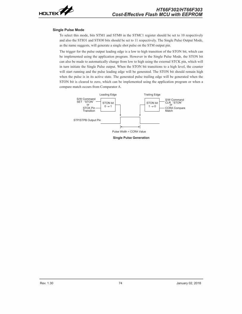
Rev. 1.30 74 ana 0 01 Rev. 1.30 75 ana 0 01
HT66F302/HT66F303Cost-Effective Flash MCU with EEPROM
HT66F302/HT66F303Cost-Effective Flash MCU with EEPROM
Single Pulse ModeToselectthismode,bitsSTM1andSTM0intheSTMC1registershouldbesetto10respectivelyandalsotheSTIO1andSTIO0bitsshouldbesetto11respectively.TheSinglePulseOutputMode,asthenamesuggests,willgenerateasingleshotpulseontheSTMoutputpin.
ThetriggerforthepulseoutputleadingedgeisalowtohightransitionoftheSTONbit,whichcanbeimplementedusingtheapplicationprogram.HoweverintheSinglePulseMode,theSTONbitcanalsobemadetoautomaticallychangefromlowtohighusingtheexternalSTCKpin,whichwillinturninitiatetheSinglePulseoutput.WhentheSTONbittransitionstoahighlevel,thecounterwillstartrunningandthepulseleadingedgewillbegenerated.TheSTONbitshouldremainhighwhenthepulseisinitsactivestate.ThegeneratedpulsetrailingedgewillbegeneratedwhentheSTONbit isclearedtozero,whichcanbeimplementedusingtheapplicationprogramorwhenacomparematchoccursfromComparatorA.
S/W Command SET“STON”
oSTCK Pin Tansition
Tailing Edge
S/W Command CLR“STON”
oCCRA Compae Match
STP/STPB Otpt Pin
Plse Width = CCRA Vale
Leading Edge
STON bit0 1
STON bit1 0
Single Pulse Generation

Rev. 1.30 74 ana 0 01 Rev. 1.30 75 ana 0 01
HT66F302/HT66F303Cost-Effective Flash MCU with EEPROM
HT66F302/HT66F303Cost-Effective Flash MCU with EEPROM
Conte Vale
CCRP
CCRA
STON
STPAU
STPOL
CCRP Int. Flag STMPF
CCRA Int. Flag STMAF
STM O/P Pin(STOC=1)
Time
Conte stopped b CCRA
PaseResme Conte Stops
b softwae
Conte Reset when STON etns high
STM [1:0] = 10 ; STIO [1:0] = 11
Plse Width set b CCRA
Otpt Invetswhen STPOL = 1
No CCRP Intepts geneated
STM O/P Pin(STOC=0)
STCK pin
Softwae Tigge
Cleaed b CCRA match
STCK pin Tigge
Ato. set b STCK pin
Softwae Tigge
Softwae Clea
Softwae TiggeSoftwae
Tigge
Single Pulse ModeNote:1.CounterstoppedbyCCRAmatch
2.CCRPisnotused3.ThepulseistriggeredbysettingtheSTONbithigh4.IntheSinglePulseMode,STIO[1:0]mustbesetto“11”andcannotbechanged.

Rev. 1.30 76 ana 0 01 Rev. 1.30 77 ana 0 01
HT66F302/HT66F303Cost-Effective Flash MCU with EEPROM
HT66F302/HT66F303Cost-Effective Flash MCU with EEPROM
HoweveracomparematchfromComparatorAwillalsoautomaticallycleartheSTONbitandthusgeneratetheSinglePulseoutputtrailingedge.InthiswaytheCCRAvaluecanbeusedtocontrolthepulsewidth.AcomparematchfromComparatorAwillalsogenerateaSTMinterrupt.Thecountercanonlyberesetback tozerowhen theSTONbitchangesfromlowtohighwhen thecounterrestarts.IntheSinglePulseModeCCRPisnotused.TheSTCCLRandSTDPXbitsarenotusedinthisMode.
Capture Input ModeToselectthismodebitsSTM1andSTM0intheSTMC1registershouldbesetto01respectively.Thismodeenablesexternalsignals tocaptureandstore thepresentvalueof theinternalcounterandcanthereforebeusedforapplicationssuchaspulsewidthmeasurements.TheexternalsignalissuppliedontheSTPI,whoseactiveedgecanbeeitherarisingedge,afallingedgeorbothrisingandfallingedges; theactiveedgetransitiontypeisselectedusingtheSTIO1andSTIO0bits intheSTMC1register.ThecounterisstartedwhentheSTONbitchangesfromlowtohighwhichisinitiatedusingtheapplicationprogram.
Whentherequirededge transitionappearson theSTPI thepresentvalue in thecounterwillbelatchedintotheCCRAregistersandaSTMinterruptgenerated.IrrespectiveofwhateventsoccurontheSTPIthecounterwillcontinuetofreerununtiltheSTONbitchangesfromhightolow.WhenaCCRPcomparematchoccursthecounterwillresetbacktozero;inthiswaytheCCRPvaluecanbeusedtocontrolthemaximumcountervalue.WhenaCCRPcomparematchoccursfromComparatorP,aSTMinterruptwillalsobegenerated.CountingthenumberofoverflowinterruptsignalsfromtheCCRPcanbeausefulmethodinmeasuringlongpulsewidths.TheSTIO1andSTIO0bitscanselect theactivetriggeredgeontheSTPItobearisingedge,fallingedgeorbothedgetypes.IftheSTIO1andSTIO0bitsarebothsethigh,thennocaptureoperationwilltakeplaceirrespectiveofwhathappensontheSTPI,howeveritmustbenotedthatthecounterwillcontinuetorun.TheSTCCLRandSTDPXbitsarenotusedinthisMode.

Rev. 1.30 76 ana 0 01 Rev. 1.30 77 ana 0 01
HT66F302/HT66F303Cost-Effective Flash MCU with EEPROM
HT66F302/HT66F303Cost-Effective Flash MCU with EEPROM
Counter Value
YY
CCRP
STON
STPAU
CCRP Int. Flag STMPF
CCRA Int. Flag STMAF
CCRA Value
Time
Counter cleared by CCRP
PauseResume
Counter Reset
STM [1:0] = 01
STM capture pin STPI
XX
Counter Stop
STIO [1:0] Value
XX YY XX YY
Active edge Active
edgeActive edge
00 – Rising edge 01 – Falling edge 10 – Both edges 11 – Disable Capture
Capture Input ModeNote:1.STM[1:0]=01andactiveedgesetbytheSTIO[1:0]bits
2.ATMCaptureinputpinactiveedgetransfersthecountervaluetoCCRA3.TheSTCCLRandSTDPXbitsarenotused4.Nooutputfunction–STOCandSTPOLbitsarenotused5.CCRPdeterminesthecountervalueandthecounterhasamaximumcountvaluewhenCCRPisequaltozero.

Rev. 1.30 7 ana 0 01 Rev. 1.30 79 ana 0 01
HT66F302/HT66F303Cost-Effective Flash MCU with EEPROM
HT66F302/HT66F303Cost-Effective Flash MCU with EEPROM
Periodic Type TM – PTMThePeriodicTypeTMcontainsfiveoperatingmodes,whichareCompareMatchOutput,Timer/EventCounter,CaptureInput,SinglePulseOutputandPWMOutputmodes.ThePeriodicTMcanalsobecontrolledwithtwoexternalinputpinsandcandrivetwoexternaloutputpins.
Device Name TM Input Pin TM Output PinHT66F30/HT66F303 10-bit PTM PTCK PTPI PTP PTPB
Note:FortheHT66F302,thePTPandPTPBpinsarenotbondedtoexternalpins.
Periodic TM OperationAtitscoreisa10-bitcount-upcounterwhichisdrivenbyauserselectableinternalorexternalclocksource.Therearetwointernalcomparatorswiththenames,ComparatorAandComparatorP.ThesecomparatorswillcomparethevalueinthecounterwiththeCCRAandCCRPregisters.
Theonlywayofchanging thevalueof the10-bitcounterusing theapplicationprogram, is toclear thecounterbychangingthePTONbit fromlowtohigh.Thecounterwillalsobeclearedautomaticallybyacounteroverfloworacomparematchwithoneof itsassociatedcomparators.Whentheseconditionsoccur,aTMinterruptsignalwillalsousuallybegenerated.ThePeriodicTypeTMcanoperateinanumberofdifferentoperationalmodes,canbedrivenbydifferentclocksourcesincludinganinputpinandcanalsocontroltheoutputpin.Alloperatingsetupconditionsareselectedusingrelevantinternalregisters.
fSYS
fSYS/4
fH/64fH/16
fTBC
PTCK
000001010011100101110111
PTCK~PTCK0
10-bit Cont-p Conte
10-bit Compaato P
CCRP
b0~b9
b0~b9
10-bit Compaato A
PTONPTPAU
Compaato A Match
Compaato P Match
Conte Clea 01
OtptContol
Polait Contol
PinContol
PTP
PTOC
PTM1 PTM0PTIO1 PTIO0
PTMAF Intept
PTMPF Intept
PTPOL PBSn
CCRA
PTCCLR
EdgeDetecto
PTPI
PTIO1 PTIO0
10
PTCKS
fTBC
PTPB
Periodic Type TM Block Diagram
Periodic Type TM Register DescriptionOveralloperationofthePeriodicTMiscontrolledusingaseriesofregisters.Areadonlyregisterpairexiststostoretheinternalcounter10-bitvalue,whiletworead/writeregisterpairsexisttostoretheinternal10-bitCCRAandCCRPvalue.Theremainingtworegistersarecontrolregisterswhichsetupthedifferentoperatingandcontrolmodes.
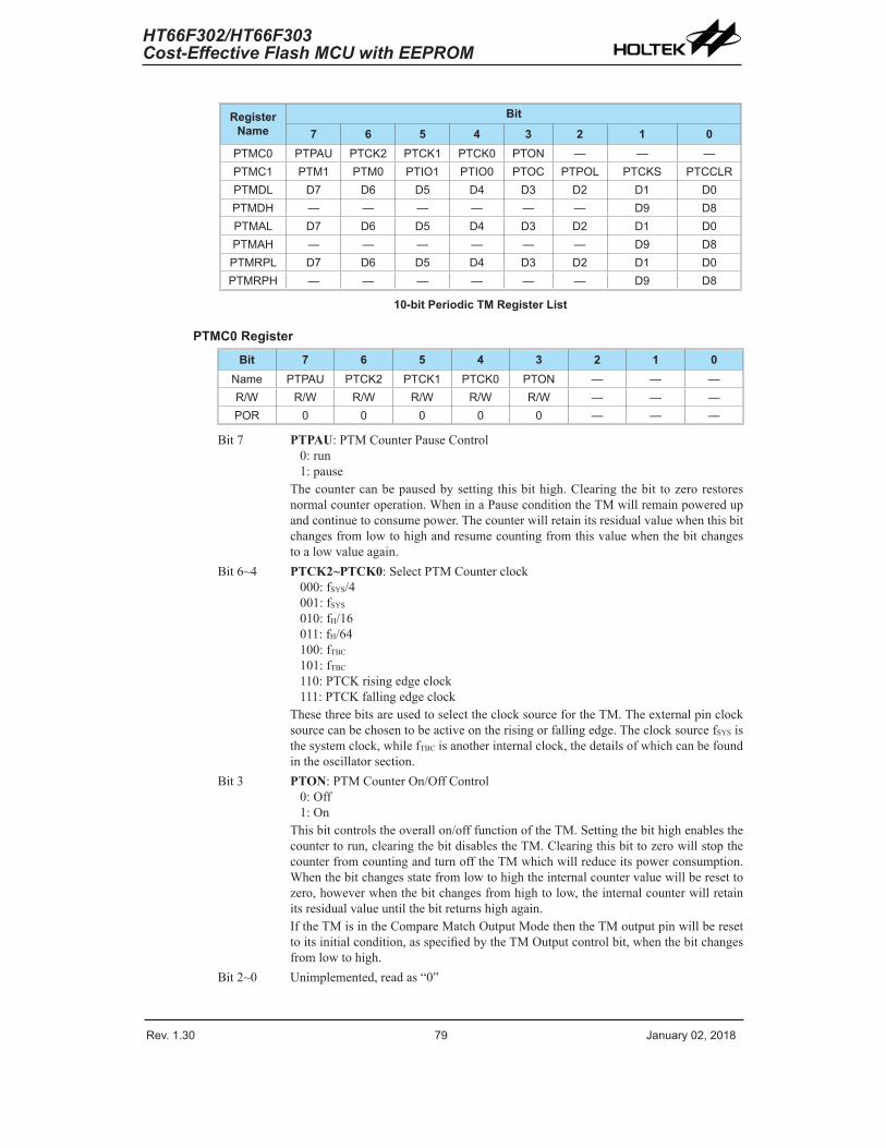
Rev. 1.30 7 ana 0 01 Rev. 1.30 79 ana 0 01
HT66F302/HT66F303Cost-Effective Flash MCU with EEPROM
HT66F302/HT66F303Cost-Effective Flash MCU with EEPROM
Register Name
Bit
7 6 5 4 3 2 1 0PTMC0 PTPAU PTCK PTCK1 PTCK0 PTON — — —PTMC1 PTM1 PTM0 PTIO1 PTIO0 PTOC PTPOL PTCKS PTCCLRPTMDL D7 D6 D5 D4 D3 D D1 D0PTMDH — — — — — — D9 DPTMAL D7 D6 D5 D4 D3 D D1 D0PTMAH — — — — — — D9 DPTMRPL D7 D6 D5 D4 D3 D D1 D0PTMRPH — — — — — — D9 D
10-bit Periodic TM Register List
PTMC0 Register
Bit 7 6 5 4 3 2 1 0Name PTPAU PTCK PTCK1 PTCK0 PTON — — —R/W R/W R/W R/W R/W R/W — — —POR 0 0 0 0 0 — — —
Bit7 PTPAU:PTMCounterPauseControl0:run1:pause
Thecountercanbepausedbysettingthisbithigh.Clearingthebit tozerorestoresnormalcounteroperation.WheninaPauseconditiontheTMwillremainpoweredupandcontinuetoconsumepower.Thecounterwillretainitsresidualvaluewhenthisbitchangesfromlowtohighandresumecountingfromthisvaluewhenthebitchangestoalowvalueagain.
Bit6~4 PTCK2~PTCK0:SelectPTMCounterclock000:fSYS/4001:fSYS
010:fH/16011:fH/64100:fTBC101:fTBC110:PTCKrisingedgeclock111:PTCKfallingedgeclock
ThesethreebitsareusedtoselecttheclocksourcefortheTM.Theexternalpinclocksourcecanbechosentobeactiveontherisingorfallingedge.TheclocksourcefSYSisthesystemclock,whilefTBCisanotherinternalclock,thedetailsofwhichcanbefoundintheoscillatorsection.
Bit3 PTON:PTMCounterOn/OffControl0:Off1:On
Thisbitcontrolstheoverallon/offfunctionoftheTM.Settingthebithighenablesthecountertorun,clearingthebitdisablestheTM.ClearingthisbittozerowillstopthecounterfromcountingandturnofftheTMwhichwillreduceitspowerconsumption.Whenthebitchangesstatefromlowtohightheinternalcountervaluewillberesettozero,howeverwhenthebitchangesfromhightolow,theinternalcounterwillretainitsresidualvalueuntilthebitreturnshighagain.IftheTMisintheCompareMatchOutputModethentheTMoutputpinwillberesettoitsinitialcondition,asspecifiedbytheTMOutputcontrolbit,whenthebitchangesfromlowtohigh.
Bit2~0 Unimplemented,readas“0”

Rev. 1.30 0 ana 0 01 Rev. 1.30 1 ana 0 01
HT66F302/HT66F303Cost-Effective Flash MCU with EEPROM
HT66F302/HT66F303Cost-Effective Flash MCU with EEPROM
PTMC1 Register
Bit 7 6 5 4 3 2 1 0Name PTM1 PTM0 PTIO1 PTIO0 PTOC PTPOL PTCKS PTCCLRR/W R/W R/W R/W R/W R/W R/W R/W R/WPOR 0 0 0 0 0 0 0 0
Bit7~6 PTM1~PTM0:SelectPTMOperationMode00:CompareMatchOutputMode01:CaptureInputMode10:PWMModeorSinglePulseOutputMode11:Timer/CounterMode
ThesebitssetuptherequiredoperatingmodefortheTM.ToensurereliableoperationtheTMshouldbeswitchedoffbeforeanychangesaremadetothePTM1andPTM0bits.IntheTimer/CounterMode,thePTMoutputpinstateisundefined.
Bit5~4 PTIO1~PTIO0:SelectPTMoutputfunctionCompareMatchOutputMode00:Nochange01:Outputlow10:Outputhigh11:Toggleoutput
PWMMode/SinglePulseOutputMode00:PWMOutputinactivestate01:PWMOutputactivestate10:PWMoutput11:Singlepulseoutput
CaptureInputMode00:InputcaptureatrisingedgeofPTPI01:InputcaptureatfallingedgeofPTPI10:Inputcaptureatfalling/risingedgeofPTPI11:Inputcapturedisabled
Timer/counterModeUnused
ThesetwobitsareusedtodeterminehowtheTMoutputpinchangesstatewhenacertainconditionisreached.ThefunctionthatthesebitsselectdependsuponinwhichmodetheTMisrunning.IntheCompareMatchOutputMode,thePTIO1andPTIO0bitsdeterminehowtheTMoutputpinchangesstatewhenacomparematchoccursfromtheComparatorA.TheTMoutputpincanbesetuptoswitchhigh,switchlowortotoggleitspresentstatewhenacomparematchoccursfromtheComparatorA.Whenthesebitsarebothzero,thennochangewill takeplaceontheoutput.TheinitialvalueoftheTMoutputpinshouldbesetupusingthePTOCbit.NotethattheoutputlevelrequestedbythePTIO1andPTIO0bitsmustbedifferent fromthe initialvaluesetupusing thePTOCbitotherwisenochangewilloccurontheTMoutputpinwhenacomparematchoccurs.AftertheTMoutputpinchangesstate,itcanberesettoitsinitiallevelbychangingthelevelofthePTONbitfromlowtohigh.In thePWMMode, thePTIO1andPTIO0bitsdeterminehowtheTMoutputpinchangesstatewhenacertaincomparematchconditionoccurs.ThePWMoutputfunctionismodifiedbychangingthesetwobits.It isnecessarytochangethevaluesofthePTIO1andPTIO0bitsonlyaftertheTMhasbeenswitchedoff.UnpredictablePWMoutputswilloccurif thePTIO1andPTIO0bitsarechangedwhentheTMisrunning.

Rev. 1.30 0 ana 0 01 Rev. 1.30 1 ana 0 01
HT66F302/HT66F303Cost-Effective Flash MCU with EEPROM
HT66F302/HT66F303Cost-Effective Flash MCU with EEPROM
Bit3 PTOC:PTP/PTPBOutputcontrolbitCompareMatchOutputMode0:Initiallow1:Initialhigh
PWMMode/SinglePulseOutputMode0:Activelow1:Activehigh
This is theoutputcontrolbit for theTMoutputpin. ItsoperationdependsuponwhetherTMisbeingusedintheCompareMatchOutputModeorinthePWMMode/SinglePulseOutputMode.IthasnoeffectiftheTMisintheTimer/CounterMode.IntheCompareMatchOutputModeitdeterminesthelogicleveloftheTMoutputpinbeforeacomparematchoccurs.InthePWMModeitdeterminesifthePWMsignalisactivehighoractivelow.
Bit2 PTPOL:PTP/PTPBOutputpolarityControl0:non-invert1:invert
ThisbitcontrolsthepolarityofthePTP/PTPBoutputpin.WhenthebitissethightheTMoutputpinwillbeinvertedandnotinvertedwhenthebitiszero.IthasnoeffectiftheTMisintheTimer/CounterMode.
Bit1 PTCKS:PTMcapturetriggersourceselect0:FromPTPI1:FromPTCKpin
Bit0 PTCCLR:SelectPTMCounterclearcondition0:PTMComparatrorPmatch1:PTMComparatrorAmatch
Thisbit isused toselect themethodwhichclears thecounter.Remember that thePeriodicTMcontains twocomparators,ComparatorAandComparatorP,eitherofwhichcanbeselectedtoclear theinternalcounter.With thePTCCLRbitsethigh,thecounterwillbeclearedwhenacomparematchoccursfromtheComparatorA.Whenthebitislow,thecounterwillbeclearedwhenacomparematchoccursfromtheComparatorPorwithacounteroverflow.AcounteroverflowclearingmethodcanonlybeimplementediftheCCRPbitsareallclearedtozero.ThePTCCLRbitisnotusedinthePWM,SinglePulseorInputCaptureMode.
PTMDL Register
Bit 7 6 5 4 3 2 1 0Name D7 D6 D5 D4 D3 D D1 D0R/W R R R R R R R RPOR 0 0 0 0 0 0 0 0
Bit7~0 PTMDL:PTMCounterLowByteRegisterbit7~bit0PTM10-bitCounterbit7~bit0
PTMDH Register
Bit 7 6 5 4 3 2 1 0Name — — — — — — D9 DR/W — — — — — — R RPOR — — — — — — 0 0
Bit7~2 Unimplemented,readas"0"Bit1~0 PTMDH:PTMCounterHighByteRegisterbit1~bit0
PTM10-bitCounterbit9~bit8

Rev. 1.30 ana 0 01 Rev. 1.30 3 ana 0 01
HT66F302/HT66F303Cost-Effective Flash MCU with EEPROM
HT66F302/HT66F303Cost-Effective Flash MCU with EEPROM
PTMAL Register
Bit 7 6 5 4 3 2 1 0Name D7 D6 D5 D4 D3 D D1 D0R/W R/W R/W R/W R/W R/W R/W R/W R/WPOR 0 0 0 0 0 0 0 0
Bit7~0 PTMAL:PTMCCRALowByteRegisterbit7~bit0PTM10-bitCCRAbit7~bit0
PTMAH Register
Bit 7 6 5 4 3 2 1 0Name — — — — — — D9 DR/W — — — — — — R/W R/WPOR — — — — — — 0 0
Bit7~2 Unimplemented,readas"0"Bit1~0 PTMAH:PTMCCRAHighByteRegisterbit1~bit0
PTM10-bitCCRAbit9~bit8
PTMRPL Register
Bit 7 6 5 4 3 2 1 0Name D7 D6 D5 D4 D3 D D1 D0R/W R/W R/W R/W R/W R/W R/W R/W R/WPOR 0 0 0 0 0 0 0 0
Bit7~0 PTMRPL:PTMCCRPLowByteRegisterbit7~bit0PTM10-bitCCRPbit7~bit0
PTMRPH Register
Bit 7 6 5 4 3 2 1 0Name — — — — — — D9 DR/W — — — — — — R/W R/WPOR — — — — — — 0 0
Bit7~2 Unimplemented,readas"0"Bit1~0 PTMRPH:PTMCCRPHighByteRegisterbit1~bit0
PTM10-bitCCRPbit9~bit8

Rev. 1.30 ana 0 01 Rev. 1.30 3 ana 0 01
HT66F302/HT66F303Cost-Effective Flash MCU with EEPROM
HT66F302/HT66F303Cost-Effective Flash MCU with EEPROM
Periodic Type TM Operating ModesThePeriodicTypeTMcanoperateinoneoffiveoperatingmodes,CompareMatchOutputMode,PWMOutputMode,SinglePulseOutputMode,CaptureInputModeorTimer/CounterMode.TheoperatingmodeisselectedusingthePTM1andPTM0bitsinthePTMC1register.
Compare Match Output ModeToselect thismode,bitsPTM1andPTM0in thePTMC1register, shouldbeallcleared to00respectively. In thismodeonce thecounter isenabledand running itcanbeclearedby threemethods.Theseareacounteroverflow,acomparematchfromComparatorAandacomparematchfromComparatorP.WhenthePTCCLRbit is low, thereare twoways inwhichthecountercanbecleared.OneiswhenacomparematchoccursfromComparatorP,theotheriswhentheCCRPbitsareallzerowhichallowsthecountertooverflow.HereboththePTMAFandPTMPFinterruptrequestflagsforComparatorAandComparatorPrespectively,willbothbegenerated.
IfthePTCCLRbitinthePTMC1registerishighthenthecounterwillbeclearedwhenacomparematchoccursfromComparatorA.However,hereonlythePTMAFinterruptrequestflagwillbegeneratedevenifthevalueoftheCCRPbitsislessthanthatoftheCCRAregisters.ThereforewhenPTCCLRishighnoPTMPFinterruptrequestflagwillbegenerated.IntheCompareMatchOutputMode,theCCRAcannotbesetto“0”.IftheCCRAbitsareallzero,thecounterwilloverflowwhenitsreachesitsmaximum10-bit,3FFHex,value,howeverherethePTMAFinterruptrequestflagwillnotbegenerated.
Asthenameofthemodesuggests,afteracomparisonismade,theTMoutputpin,willchangestate.TheTMoutputpinconditionhoweveronlychangesstatewhenaPTMAFinterruptrequestflagisgeneratedafteracomparematchoccursfromComparatorA.ThePTMPFinterruptrequestflag,generatedfromacomparematchfromComparatorP,willhavenoeffectontheTMoutputpin.ThewayinwhichtheTMoutputpinchangesstatearedeterminedbytheconditionofthePTIO1andPTIO0bitsinthePTMC1register.TheTMoutputpincanbeselectedusingthePTIO1andPTIO0bitstogohigh,togolowortotogglefromitspresentconditionwhenacomparematchoccursfromComparatorA.TheinitialconditionoftheTMoutputpin,whichissetupafterthePTONbitchangesfromlowtohigh,issetupusingthePTOCbit.NotethatifthePTIO1,PTIO0bitsarezerothennopinchangewilltakeplace.

Rev. 1.30 4 ana 0 01 Rev. 1.30 5 ana 0 01
HT66F302/HT66F303Cost-Effective Flash MCU with EEPROM
HT66F302/HT66F303Cost-Effective Flash MCU with EEPROM
Conte Vale
0x3FF
CCRP
CCRA
PTON
PTPAU
PTPOL
CCRP Int. Flag PTMPF
CCRA Int. Flag PTMAF
PTM O/P Pin
Time
CCRP=0
CCRP > 0
Conte oveflowCCRP > 0Conte cleaed b CCRP vale
Pase
Resme
Stop
Conte Restat
Otpt pin set to initial Level Low if PTOC=0
Otpt Toggle with PTMAF flag
Note PTIO [1:0] = 10 Active High Otpt select
Hee PTIO [1:0] = 11 Toggle Otpt select
Otpt not affected b PTMAF flag. Remains High ntil eset b PTON bit
Otpt PinReset to Initial vale
Otpt contolled b othe pin-shaed fnction
Otpt Invetswhen PTPOL is high
PTCCLR = 0; PTM [1:0] = 00
Compare Match Output Mode – PTCCLR=0Note:1.WithPTCCLR=0–aComparatorPmatchwillclearthecounter
2.TheTMoutputpiniscontrolledonlybythePTMAFflag3.TheoutputpinisresettoinitialstatebyaPTONbitrisingedge

Rev. 1.30 4 ana 0 01 Rev. 1.30 5 ana 0 01
HT66F302/HT66F303Cost-Effective Flash MCU with EEPROM
HT66F302/HT66F303Cost-Effective Flash MCU with EEPROM
Conte Vale
0x3FF
CCRP
CCRA
PTON
PTPAU
PTPOL
CCRP Int. Flag PTMPF
CCRA Int. Flag PTMAF
PTM O/P Pin
Time
CCRA=0
CCRA = 0Conte oveflowCCRA > 0 Conte cleaed b CCRA vale
Pase
Resme
Stop Conte Restat
Otpt pin set to initial Level Low if PTOC=0
Otpt Toggle with PTMAF flag
Note PTIO [1:0] = 10 Active High Otpt select
Hee PTIO [1:0] = 11 Toggle Otpt select
Otpt not affected b PTMAF flag. Remains High ntil eset b PTON bit
Otpt PinReset to Initial vale
Otpt contolled b othe pin-shaed fnction
Otpt Invetswhen PTPOL is high
PTMPF not geneated
No PTMAF flag geneated on CCRA oveflow
Otpt does not change
PTCCLR = 1; PTM [1:0] = 00
Compare Match Output Mode – PTCCLR=1Note:1.WithPTCCLR=1–aComparatorAmatchwillclearthecounter
2.TheTMoutputpiniscontrolledonlybythePTMAFflag3.TheoutputpinisresettoinitialstatebyaPTONrisingedge4.ThePTMPFflagisnotgeneratedwhenPTCCLR=1

Rev. 1.30 6 ana 0 01 Rev. 1.30 7 ana 0 01
HT66F302/HT66F303Cost-Effective Flash MCU with EEPROM
HT66F302/HT66F303Cost-Effective Flash MCU with EEPROM
Timer/Counter ModeToselectthismode,bitsPTM1andPTM0inthePTMC1registershouldallbesetto11respectively.TheTimer/CounterModeoperates in an identicalway to theCompareMatchOutputModegeneratingthesameinterruptflags.TheexceptionisthatintheTimer/CounterModetheTMoutputpin isnotused.Therefore theabovedescriptionandTimingDiagramsfor theCompareMatchOutputModecanbeusedtounderstanditsfunction.AstheTMoutputpinisnotusedinthismode,thepincanbeusedasanormalI/Opinorotherpin-sharedfunction.
PWM Output ModeToselectthismode,bitsPTM1andPTM0inthePTMC1registershouldbesetto10respectivelyandalso thePTIO1andPTIO0bitsshouldbeset to10respectively.ThePWMfunctionwithintheTMisusefulforapplicationswhichrequirefunctionssuchasmotorcontrol,heatingcontrol,illuminationcontroletc.ByprovidingasignaloffixedfrequencybutofvaryingdutycycleontheTMoutputpin,asquarewaveACwaveformcanbegeneratedwithvaryingequivalentDCRMSvalues.
AsboththeperiodanddutycycleofthePWMwaveformcanbecontrolled,thechoiceofgeneratedwaveformisextremelyflexible.In thePWMmode, thePTCCLRbithasnoeffectas thePWMperiod.BothoftheCCRPandCCRAregistersareusedtogeneratethePWMwaveform,oneregisterisusedtocleartheinternalcounterandthuscontrolthePWMwaveformfrequency,whiletheotheroneisusedtocontrolthedutycycle.ThePWMwaveformfrequencyanddutycyclecanthereforebecontrolledbythevaluesintheCCRAandCCRPregisters.
Aninterruptflag,oneforeachoftheCCRAandCCRP,willbegeneratedwhenacomparematchoccursfromeitherComparatorAorComparatorP.ThePTOCbitinthePTMC1registerisusedtoselecttherequiredpolarityofthePWMwaveformwhilethetwoPTIO1andPTIO0bitsareusedtoenablethePWMoutputortoforcetheTMoutputpintoafixedhighorlowlevel.ThePTPOLbitisusedtoreversethepolarityofthePWMoutputwaveform.
• 10-bit PWM Mode, PWM Mode
CCRP 1~1023 0Peiod 1~103 104Dt CCRA
IffSYS=8MHz,TMclocksourceselectfSYS/4,CCRP=512andCCRA=128,
ThePTMPWMoutputfrequency=(fSYS/4)/(2×256)=fSYS/2048=3.90625kHz,duty=128/512=25%,
IftheDutyvaluedefinedbytheCCRAregisterisequaltoorgreaterthanthePeriodvalue,thenthePWMoutputdutyis100%.

Rev. 1.30 6 ana 0 01 Rev. 1.30 7 ana 0 01
HT66F302/HT66F303Cost-Effective Flash MCU with EEPROM
HT66F302/HT66F303Cost-Effective Flash MCU with EEPROM
Conte Vale
CCRP
CCRA
PTON
PTPAU
PTPOL
CCRP Int. Flag PTMPF
CCRA Int. Flag PTMAF
PTM O/P Pin(PTOC=1)
Time
Conte cleaed b CCRP
Pase Resme Conte Stop if PTON bit low
Conte Reset when PTON etns high
PWM Dt Ccle set b CCRA
PWM esmes opeation
Otpt contolled b othe pin-shaed fnction Otpt Invets
When PTPOL = 1PWM Peiod set b CCRP
PTM O/P Pin(PTOC=0)
PTM [1:0] = 10
PWM Output ModeNote:1.HereCounterclearedbyCCRP
2.AcounterclearsetsthePWMPeriod3.TheinternalPWMfunctioncontinuesrunningevenwhenPTIO[1:0]=00or014.ThePTCCLRbithasnoinfluenceonPWMoperation

Rev. 1.30 ana 0 01 Rev. 1.30 9 ana 0 01
HT66F302/HT66F303Cost-Effective Flash MCU with EEPROM
HT66F302/HT66F303Cost-Effective Flash MCU with EEPROM
Single Pulse Output ModeToselectthismode,therequiredbitpairs,PTM1andPTM0shouldbesetto10respectivelyandalsothecorrespondingPTIO1andPTIO0bitsshouldbeset to11respectively.TheSinglePulseOutputMode,asthenamesuggests,willgenerateasingleshotpulseontheTMoutputpin.
ThetriggerforthepulseoutputleadingedgeisalowtohightransitionofthePTONbit,whichcanbeimplementedusingtheapplicationprogram.HoweverintheSinglePulseMode,thePTONbitcanalsobemadetoautomaticallychangefromlowtohighusingtheexternalPTCKpin,whichwillinturninitiatetheSinglePulseoutput.WhenthePTONbittransitionstoahighlevel,thecounterwillstartrunningandthepulseleadingedgewillbegenerated.ThePTONbitshouldremainhighwhenthepulseisinitsactivestate.ThegeneratedpulsetrailingedgewillbegeneratedwhenthePTONbit isclearedtozero,whichcanbeimplementedusingtheapplicationprogramorwhenacomparematchoccursfromComparatorA.
HoweveracomparematchfromComparatorAwillalsoautomaticallyclearthePTONbitandthusgeneratetheSinglePulseoutputtrailingedge.InthiswaytheCCRAvaluecanbeusedtocontrolthepulsewidth.AcomparematchfromComparatorAwillalsogenerateTMinterrupts.ThecountercanonlyberesetbacktozerowhenthePTONbitchangesfromlowtohighwhenthecounterrestarts.IntheSinglePulseModeCCRPisnotused.ThePTCCLRbitisalsonotused.
S/W Command SET“PTON”
oPTCK Pin Tansition
Tailing Edge
S/W Command CLR“PTON”
oCCRA Compae Match
PTP/PTPB Otpt Pin
Plse Width = CCRA Vale
Leading Edge
PTON bit0 → 1
PTON bit1 → 0
Single Pulse Generation

Rev. 1.30 ana 0 01 Rev. 1.30 9 ana 0 01
HT66F302/HT66F303Cost-Effective Flash MCU with EEPROM
HT66F302/HT66F303Cost-Effective Flash MCU with EEPROM
Conte Vale
CCRP
CCRA
PTON
PTPAU
PTPOL
CCRP Int. Flag PTMPF
CCRA Int. Flag PTMAF
PTM O/P Pin(PTOC=1)
Time
Conte stopped b CCRA
PaseResme Conte Stops
b softwae
Conte Reset when PTON etns high
Plse Width set b CCRA
Otpt Invetswhen PTPOL = 1
No CCRP Intepts geneated
PTM O/P Pin(PTOC=0)
PTCK pin
Softwae Tigge
Cleaed b CCRA match
PTCK pin Tigge
Ato. set b PTCK pin
Softwae Tigge
Softwae Clea
Softwae TiggeSoftwae
Tigge
PTM [1:0] = 10 ; PTIO [1:0] = 11
Single Pulse ModeNote:1.CounterstoppedbyCCRA
2.CCRPisnotused3.ThepulseistriggeredbythePTCKpinorbysettingthePTONbithigh4.APTCKpinactiveedgewillautomaticallysetthePTONbithigh5.IntheSinglePulseMode,PTIO[1:0]mustbesetto“11”andcannotbechanged.

Rev. 1.30 90 ana 0 01 Rev. 1.30 91 ana 0 01
HT66F302/HT66F303Cost-Effective Flash MCU with EEPROM
HT66F302/HT66F303Cost-Effective Flash MCU with EEPROM
Capture Input ModeToselectthismodebitsPTM1andPTM0inthePTMC1registershouldbesetto01respectively.Thismodeenablesexternalsignals tocaptureandstore thepresentvalueof theinternalcounterandcanthereforebeusedforapplicationssuchaspulsewidthmeasurements.TheexternalsignalissuppliedonthePTPIorPTCKpin,selectedbythePTCKSbitinthePTMC1register.Theinputpinactiveedgecanbeeitherarisingedge,afallingedgeorbothrisingandfallingedges;theactiveedgetransitiontypeisselectedusingthePTIO1andPTIO0bitsinthePTMC1register.ThecounterisstartedwhenthePTONbitchangesfromlowtohighwhich is initiatedusing theapplicationprogram.
WhentherequirededgetransitionappearsonthePTPIorPTCKpinthepresentvalueinthecounterwillbelatchedintotheCCRAregisterandaTMinterruptgenerated.IrrespectiveofwhateventsoccuronthePTPIorPTCKpinthecounterwillcontinuetofreerununtil thePTONbitchangesfromhightolow.WhenaCCRPcomparematchoccursthecounterwillresetbacktozero;inthiswaytheCCRPvaluecanbeusedtocontrolthemaximumcountervalue.WhenaCCRPcomparematchoccursfromComparatorP,aTMinterruptwillalsobegenerated.CountingthenumberofoverflowinterruptsignalsfromtheCCRPcanbeausefulmethodinmeasuringlongpulsewidths.ThePTIO1andPTIO0bitscanselecttheactivetriggeredgeonthePTPIorPTCKpintobearisingedge,fallingedgeorbothedgetypes.IfthePTIO1andPTIO0bitsarebothsethigh,thennocaptureoperationwilltakeplaceirrespectiveofwhathappensonthePTPIorPTCKpin,howeveritmustbenotedthatthecounterwillcontinuetorun.
AsthePTPIorPTCKpinispinsharedwithotherfunctions,caremustbetakenifthePTMisintheCaptureInputMode.Thisisbecauseifthepinissetupasanoutput,thenanytransitionsonthispinmaycauseaninputcaptureoperationtobeexecuted.ThePTCCLR,PTOCandPTPOLbitsarenotusedinthisMode.

Rev. 1.30 90 ana 0 01 Rev. 1.30 91 ana 0 01
HT66F302/HT66F303Cost-Effective Flash MCU with EEPROM
HT66F302/HT66F303Cost-Effective Flash MCU with EEPROM
Conte Vale
YY
CCRP
PTON
PTPAU
CCRP Int. Flag PTMPF
CCRA Int. Flag PTMAF
CCRA Vale
Time
Conte cleaed b CCRP
PaseResme
Conte Reset
PTM [1:0] = 01
PTM capte pinPTPI o PTCK
XX
Conte Stop
PTIO [1:0] Vale
XX YY XX YY
Active edge Active
edgeActive edge
00 – Rising edge 01 – Falling edge 10 – Both edges 11 – Disable Capte
Capture Input ModeNote:1.PTM[1:0]=01andactiveedgesetbythePTIO[1:0]bits
2.ATMCaptureinputpinactiveedgetransferscountervaluetoCCRA3.ThePTCCLRbitisnotused4.Nooutputfunction–PTOCandPTPOLbitsarenotused5.CCRPdeterminesthecountervalueandthecounterhasamaximumcountvaluewhenCCRPisequaltozero

Rev. 1.30 9 ana 0 01 Rev. 1.30 93 ana 0 01
HT66F302/HT66F303Cost-Effective Flash MCU with EEPROM
HT66F302/HT66F303Cost-Effective Flash MCU with EEPROM
Analog to Digital Converter – ADCTheneedtointerfacetorealworldanalogsignals isacommonrequirementformanyelectronicsystems.However, toproperlyprocess these signalsbyamicrocontroller, theymust firstbeconverted intodigitalsignalsbyA/Dconverters.By integrating theA/Dconversionelectroniccircuitryintothemicrocontroller,theneedforexternalcomponentsisreducedsignificantlywiththecorrespondingfollow-onbenefitsoflowercostsandreducedcomponentspacerequirements.
A/D OverviewThedevicescontainamulti-channelanalog todigital converterwhichcandirectly interfacetoexternalanalogsignals, suchas that fromsensorsorothercontrolsignalsandconvert thesesignalsdirectlyintoa12-bitdigitalvalue.Theexternalor internalanalogsignal tobeconvertedisdeterminedby theSAINSandSACSbit fields.Note thatwhen the internalanalogsignal istobeconverted, theselectedexternal inputchannelwillautomaticallybedisconnected toavoidmalfunction.Moredetailed informationabout theA/D input signal isdescribed in the“A/DConverterControlRegisters”and“A/DConverterInputSignal”sectionsrespectively.
Device Input Channels A/D Channel Select Bits Input Pins
HT66F30/HT66F303 4 SAINS~SAINS0SACS1~SACS0 AN0~AN3
TheaccompanyingblockdiagramshowstheoverallinternalstructureoftheA/Dconverter,togetherwithitsassociatedregisters.
Pin-shared selection SACS1~SACS0
SAINS2~SAINS0
A/D Converter
START ADBZ ENADC
AVSS
A/D Clock
÷ 2N
(N=0~7)
fSYS
SACKS2~SACKS0
AVDD
ENADC
SADOL
SADOH
AN0
AN1
AN3 A/D Reference Voltage
A/D DataRegisters
AVDD
AVDD/2
AVDD/4
ADRFS
OPA(Gain=1~4)
VRI
VREFI
VBG (1.0V)
SAVRS3~SAVRS0
ENOPA
VREFO
VR
AVDD
VREFO
VREFI
A/D Converter Structure

Rev. 1.30 9 ana 0 01 Rev. 1.30 93 ana 0 01
HT66F302/HT66F303Cost-Effective Flash MCU with EEPROM
HT66F302/HT66F303Cost-Effective Flash MCU with EEPROM
A/D Converter Register DescriptionOveralloperationof theA/Dconverteriscontrolledusingsixregisters.AreadonlyregisterpairexiststostoretheADCdata12-bitvalue.TheremainingfourregistersarecontrolregisterswhichsetuptheoperatingandcontrolfunctionoftheA/Dconverter.
Register NameBit
7 6 5 4 3 2 1 0SADOL(ADRFS=0) D3 D D1 D0 — — — —SADOL(ADRFS=1) D7 D6 D5 D4 D3 D D1 D0SADOH(ADRFS=0) D11 D10 D9 D D7 D6 D5 D4SADOH(ADRFS=1) — — — — D11 D10 D9 DSADC0 START ADBZ ENADC ADRFS — — SACS1 SACS0SADC1 SAINS SAINS1 SAINS0 — — SACKS SACKS1 SACKS0SADC ENOPA VBGEN VREFI VREFO SAVRS3 SAVRS SAVRS1 SAVRS0PASR PAS7 PAS6 PAS5 PAS4 PAS3 PAS PAS1 PAS0
A/D Converter Register List
A/D Converter Data Registers – SADOL, SADOHAsthedevicescontainaninternal12-bitA/Dconverter, itrequirestwodataregisterstostoretheconvertedvalue.Theseareahighbyteregister,knownasSADOH,andalowbyteregister,knownasSADOL.After theconversionprocess takesplace, theseregisterscanbedirectlyreadbythemicrocontrollertoobtainthedigitisedconversionvalue.Asonly12bitsofthe16-bitregisterspaceisutilised, theformat inwhichthedata isstorediscontrolledbytheADRFSbit in theSADC0registerasshownintheaccompanyingtable.D0~D11aretheA/Dconversionresultdatabits.Anyunusedbitswillbereadaszero.NotethattheA/DconverterdataregistercontentswillbeclearedtozeroiftheA/Dconverterisdisabled.
ADRFSSADOH SADOL
7 6 5 4 3 2 1 0 7 6 5 4 3 2 1 00 D11 D10 D9 D D7 D6 D5 D4 D3 D D1 D0 0 0 0 01 0 0 0 0 D11 D10 D9 D D7 D6 D5 D4 D3 D D1 D0
A/D Data Registers
A/D Converter Control Registers – SADC0, SADC1, SADC2, PASRTocontrol thefunctionandoperationof theA/Dconverter,severalcontrol registersknownasSADC0,SADC1andSADC2areprovided.These8-bit registersdefine functionssuchas theselectionofwhichanalogchannel isconnected to the internalA/Dconverter, thedigitiseddataformat, theA/Dclocksourceaswellascontrolling thestart functionandmonitoring theA/Dconverterbusystatus.Asthedevicescontainonlyoneactualanalogtodigitalconverterhardwarecircuit, eachof theexternaland internalanalogsignalsmustbe routed to theconverter.TheSACS1~SACS0bitsintheSADC0registerareusedtodeterminewhichexternalchannelinputisselectedtobeconverted.TheSAINS2~SAINS0bitsintheSADC1registerareusedtodeterminethat theanalogsignal tobeconvertedcomesfromthe internalanalogsignalorexternalanalogchannelinput.IftheSAINS2~SAINS0bitsaresetto“000”or“100”,theexternalanalogchannelinputisselectedtobeconvertedandtheSACS1~SACS0bitscandeterminewhichexternalchannelisselectedtobeconverted.IftheSAINS2~SAINS0bitsaresettoanyothervaluesexcept“000”and“100”,oneoftheinternalanalogsignalsisselectedtobeconverted.TheinternalanalogsignalscanbederivedfromtheA/Dconvertersupplypower,AVDD,withaspecificratioof1,1/2or1/4.Iftheinternalanalogsignalisselectedtobeconverted,theexternalchannelsignalinputwillautomaticallybeswitchedofftoavoidthesignalcontention.

Rev. 1.30 94 ana 0 01 Rev. 1.30 95 ana 0 01
HT66F302/HT66F303Cost-Effective Flash MCU with EEPROM
HT66F302/HT66F303Cost-Effective Flash MCU with EEPROM
Thepin-shared functioncontrol registernamedPASR,contains thecorrespondingpin-sharedselectionbitswhichdeterminewhichpinsonPortAareusedasanaloginputsfortheA/DconverterinputandwhichpinsarenottobeusedastheA/Dconverterinput.WhenthepinisselectedtobeanA/Dinput,itsoriginalfunctionwhetheritisanI/Oorotherpin-sharedfunctionwillberemoved.Inaddition,anyinternalpull-highresistorsconnectedtothesepinswillbeautomaticallyremovedifthepinisselectedtobeanA/Dinput.
SAINS [2:0] SACS [1:0] Input Signals Description000 100 00~11 AN0~AN3 Extenal channel analog inpt
001 xxx VDD A/D convete powe sppl voltage010 xxx VDD/ A/D convete powe sppl voltage/011 xxx VDD/4 A/D convete powe sppl voltage/4
A/D Converter Input Signal Selection
SADC0 Register
Bit 7 6 5 4 3 2 1 0Name START ADBZ ENADC ADRFS SACS1 SACS0R/W R/W R R/W R/W R/W R/WPOR 0 0 0 0 0 0
Bit7 START:StarttheA/Dconversion0→1→0:StartA/Dconversion0→1:ResettheA/DconverterandsetADBZto01→0:StartA/DconversionandsetADBZto1
ThisbitisusedtoinitiateanA/Dconversionprocess.Thebitisnormallylowbutifsethighandthenclearedlowagain,theA/Dconverterwillinitiateaconversionprocess.
Bit6 ADBZ:A/DConverterbusyflag0:NoA/Dconversionisinprogress1:A/Dconversionisinprogress
ThisreadonlyflagisusedtoindicatewhethertheA/Dconversionis inprogressornot.WhentheSTARTbitissetfromlowtohighandthentolowagain,theADBZflagwillbesethightoindicatethattheA/Dconversionisinitiated.TheADBZflagwillbeclearedtozeroaftertheA/Dconversioniscomplete.
Bit5 ENADC:A/DConverterfunctionenablecontrol0:Disable1:Enable
ThisbitcontrolstheA/Dinternalfunction.ThisbitshouldbesethightoenabletheA/Dconverter.Ifthebitissetlow,thentheA/Dconverterwillbeswitchedoffreducingthedevicepowerconsumption.When theA/Dconverter function isdisabled, thecontentsoftheA/Ddataregisterpair,SADOHandSADOL,willbeclearedtozero.
Bit4 ADRFS:A/DConverterdataformatcontrol0:ADCoutputdataformat→SADOH=D[11:4];SADOL=D[3:0]1:ADCoutputdataformat→SADOH=D[11:8];SADOL=D[7:0]
Thisbitcontrols theformatof the12-bitconvertedA/Dvaluein thetwoA/Ddataregisters.DetailsareprovidedintheA/Dconverterdataregistersection.
Bit3~2 Unimplemented,readas“0”Bit1~0 SACS1~SACS0:A/Dconverterexternalanaloginputchannelselection
00:AN001:AN110:AN211:AN3

Rev. 1.30 94 ana 0 01 Rev. 1.30 95 ana 0 01
HT66F302/HT66F303Cost-Effective Flash MCU with EEPROM
HT66F302/HT66F303Cost-Effective Flash MCU with EEPROM
SADC1 Register
Bit 7 6 5 4 3 2 1 0Name SAINS SAINS1 SAINS0 SACKS SACKS1 SACKS0R/W R/W R/W R/W R/W R/W R/WPOR 0 0 0 0 0 0
Bit7~5 SAINS2~SAINS0:A/Dconverterinputsignalselection000,100:Externalsignal–Externalanalogchannelinput001:Internalsignal–InternalA/DconverterpowersupplyvoltageAVDD
010:Internalsignal–InternalA/DconverterpowersupplyvoltageAVDD/2011:Internalsignal–InternalA/DconverterpowersupplyvoltageAVDD/4101,110,111:Reserved
Whentheinternalanalogsignalisselectedtobeconverted,theexternalchannelinputsignalwillautomaticallybeswitchedoffregardlessof theSACS1~SACS0bitfieldvalue.
Bit4~3 Unimplemented,readas“0”Bit2~0 SACKS2~SACKS0:A/Dconversionclocksourceselection
000:fSYS
001:fSYS/2010:fSYS/4011:fSYS/8100:fSYS/16101:fSYS/32110:fSYS/64111:fSYS/128
SADC2 Register
Bit 7 6 5 4 3 2 1 0Name ENOPA VBGEN VREFI VREFO SAVRS3 SAVRS SAVRS1 SAVRS0R/W R/W R/W R/W R/W R/W R/W R/W R/WPOR 0 0 0 0 0 0 0 0
Bit7 ENOPA:A/DconverterOPAenable/disablecontrol0:Disable1:Enable
Thisbitcontrols theinternalOPAfunctiontoprovidevariousreferencevoltagefortheA/Dconverter.Whenthebitissethigh,theinternalreferencevoltage,VR,canbeusedastheinternalconvertersignalorreferencevoltagebytheA/Dconverter.Iftheinternalreferencevoltage isnotusedbytheA/Dconverter, thentheOPAfunctionshouldbeproperlyconfiguredtoconservepower.
Bit6 VBGEN:InternalBandgapreferencevoltageenablecontrol0:Disable1:Enable
This iscontrols the internalBandgapcircuiton/off function to theA/Dconverter.When thebit is sethigh, theBandgap referencevoltagecanbeusedby theA/Dconverter.IftheBandgapreferencevoltageisnotusedbytheA/DconverterandtheLVRfunctionisdisabled, thenthebandgapreferencecircuitwillbeautomaticallyswitchedofftoconservepower.WhentheBandgapreferencevoltageisswitchedonforusebytheA/Dconverter,atime,tBGS,shouldbeallowedfortheBandgapcircuittostabilisebeforeimplementinganA/Dconversion.

Rev. 1.30 96 ana 0 01 Rev. 1.30 97 ana 0 01
HT66F302/HT66F303Cost-Effective Flash MCU with EEPROM
HT66F302/HT66F303Cost-Effective Flash MCU with EEPROM
Bit5 VREFI:VREFIinputcontrol0:Disable1:Enable
Bit4 VREFO:VREFOoutputcontrol0:Disable1:Enable
Bit3~0 SAVRS3~SAVRS0:A/Dconverterreferencevoltageselection0000:AVDD
0001:VREFI
0010:VREFI×20011:VREFI×30100:VREFI×41001:Inhibittouse1010:VBG×21011:VBG×31100:VBG×4Others:AVDD
When theA/Dconverter referencevoltagesource is selected toderive from theinternalVBGvoltage,thereferencevoltagewhichcomesfromtheAVDDorVREFIpinwillbeautomaticallyswitchedoff.
A/D OperationTheSTARTbitisusedtostartandresettheA/Dconverter.Whenthemicrocontrollersetsthisbitfromlowtohighandthenlowagain,ananalogtodigitalconversioncyclewillbeinitiated.WhentheSTARTbitisbroughtfromlowtohighbutnotlowagain,theADBZbitintheSADC0registerwillbeclearedtozeroandtheanalogtodigitalconverterwillbereset.ItistheSTARTbitthatisusedtocontroltheoverallstartoperationoftheinternalanalogtodigitalconverter.
TheADBZbit intheSADC0registerisusedtoindicatewhethertheanalogtodigitalconversionprocessis inprocessornot.WhentheA/Dconverter isresetbysettingtheSTARTbitfromlowtohigh, theADBZflagwillbecleared to“0”.Thisbitwillbeautomaticallyset to“1”by themicrocontrollerafteranA/Dconversion issuccessfully initiated.When theA/Dconversion iscomplete,theADBZwillbeclearedto“0”.Inaddition,thecorrespondingA/Dinterruptrequestflagwillbesetintheinterruptcontrolregister,andiftheinterruptsareenabled,anappropriateinternalinterruptsignalwillbegenerated.ThisA/DinternalinterruptsignalwilldirecttheprogramflowtotheassociatedA/Dinternalinterruptaddressforprocessing.IftheA/Dinternalinterruptisdisabled,themicrocontrollercanbeusedtopolltheADBZbitintheSADC0registertocheckwhetherithasbeenclearedasanalternativemethodofdetectingtheendofanA/Dconversioncycle.
TheclocksourcefortheA/Dconverter,whichoriginatesfromthesystemclockfSYS,canbechosentobeeither fSYSorasubdividedversionof fSYS.Thedivisionratiovalue isdeterminedby theSACKS2~SACKS0bits intheSADC1register.AlthoughtheA/DclocksourceisdeterminedbythesystemclockfSYS,andbybitsSACKS2~SACKS0,therearesomelimitationsonthemaximumA/Dclocksourcespeedthatcanbeselected.AstherecommendedvalueofpermissibleA/Dclockperiod,tADCK,isfrom0.5μsto10μs,caremustbetakenforsystemclockfrequencies.Forexample,ifthesystemclockoperatesatafrequencyof4MHz,theSACKS2~SACKS0bitsshouldnotbesetto“000”,“110”or“111”.DoingsowillgiveA/DclockperiodsthatarelessthantheminimumA/Dclockperiodorgreater thanthemaximumA/Dclockperiodwhichmayresult ininaccurateA/Dconversionvalues.Refertothefollowingtableforexamples,wherevaluesmarkedwithanasterisk*showwhere,dependinguponthedevice,specialcaremustbetaken.

Rev. 1.30 96 ana 0 01 Rev. 1.30 97 ana 0 01
HT66F302/HT66F303Cost-Effective Flash MCU with EEPROM
HT66F302/HT66F303Cost-Effective Flash MCU with EEPROM
fSYS
A/D Clock Period (tADCK)SACKS2,SACKS1,SACKS0
=000(fSYS)
SACKS2,SACKS1,SACKS0
=001(fSYS/2)
SACKS2,SACKS1, SACKS0
=010(fSYS/4)
SACKS2,SACKS1, SACKS0
=011(fSYS/8)
SACKS2,SACKS1,SACKS0
=100(fSYS/16)
SACKS2,SACKS1,SACKS0
=101(fSYS/32)
SACKS2,SACKS1,SACKS0
=110(fSYS/64)
SACKS2,SACKS1,SACKS0
=111(fSYS/128)
1MHz 1μs 2μs 4μs 8μs 16μs* 32μs* 64μs* 128μs*MHz 500ns 1μs 2μs 4μs 8μs 16μs* 32μs* 64μs*4MHz 50ns* 500ns 1μs 2μs 4μs 8μs 16μs* 32μs*MHz 15ns* 50ns* 500ns 1μs 2μs 4μs 8μs 16μs*
A/D Clock Period Examples
Controlling thepoweron/off functionof theA/Dconvertercircuitry is implementedusing theENADCbitintheSADC0register.ThisbitmustbesethightopowerontheA/Dconverter.WhentheENADCbit issethigh topoweron theA/Dconverter internalcircuitryacertaindelay,asindicatedin the timingdiagram,mustbeallowedbeforeanA/Dconversionis initiated.EvenifnopinsareselectedforuseasA/Dinputsbyconfiguringthecorrespondingpincontrolbits,iftheENADCbitishighthensomepowerwillstillbeconsumed.Inpowerconsciousapplicationsit isthereforerecommendedthat theENADCisset lowtoreducepowerconsumptionwhentheA/Dconverterfunctionisnotbeingused.
A/D Reference VoltageThereferencevoltagesupplytotheA/DConvertercanbesuppliedfromthepositivepowersupplypin,AVDD,anexternalreferencesourcesuppliedonpinVREFIoran internalreferencesourcederivedfromtheBandgapcircuit.Then theselectedreferencevoltagesourcecanbeamplifiedthroughanoperationalamplifierexcepttheonesourcedfromAVDD.TheOPAgaincanbeequalto1,2,3or4.ThedesiredselectionismadeusingtheSAVRS3~SAVRS0bitsintheSADC2registerandrelevantpinfunctioncontrolbits.NotethatthedesiredselectedreferencevoltagewillbeoutputontheVREFOpinwhichispin-sharedwithotherfunctions.AstheVREFIandVREFOpinsbotharepin-sharedwithotherfunctions,whentheVREFIorVREFOpinisselectedas thereferencevoltagesupplypin,thepinfunctioncontrolbitVREFIorVREFOshouldbesethightodisableotherpin-sharedfunctions.WhenVREFIorVBGisselectedbyADCreferencevoltage, theOPAneedstobeenabledbysettingtheENOPAbitto“1”.Inaddition,if theprogramsselectexternalreferencevoltageVREFIandtheinternalreferencevoltageVBGasADCreferencevoltage, thenthehardwarewillonlychoosetheinternalreferencevoltageVBGasanADCreferencevoltageinput.
SAVRS[3:0] Reference Description0000/othes AVDD ADC Refeence Voltage comes fom AVDD
0001 VREF ADC Refeence Voltage comes fom Extenal VREFI
0010 VREF× ADC Refeence Voltage comes fom Extenal VREFI×0011 VREF×3 ADC Refeence Voltage comes fom Extenal VREFI×30100 VREF×4 ADC Refeence Voltage comes fom Extenal VREFI×41010 VBG× ADC Refeence Voltage comes fom VBG×1011 VBG×3 ADC Refeence Voltage comes fom VBG×31100 VBG×4 ADC Refeence Voltage comes fom VBG×4
A/D Converter Reference Voltage Selection

Rev. 1.30 9 ana 0 01 Rev. 1.30 99 ana 0 01
HT66F302/HT66F303Cost-Effective Flash MCU with EEPROM
HT66F302/HT66F303Cost-Effective Flash MCU with EEPROM
A/D Converter Input SignalAlloftheA/Danaloginputpinsarepin-sharedwiththeI/OpinsonPortAaswellasotherfunctions.ThecorredpondingselectionbitsforeachI/OpininthePASRregister,determinewhethertheinputpinsaresetupasA/Dconverteranaloginputsorwhethertheyhaveotherfunctions.Ifthepin-sharedfunctioncontrolbitsconfigureitscorrespondingpinasanA/Danalogchannelinput, thepinwillbesetuptobeanA/Dconverterexternalchannelinputandtheoriginalpinfunctionsdisabled.Inthisway,pinscanbechangedunderprogramcontroltochangetheirfunctionbetweenA/Dinputsandotherfunctions.Allpull-highresistors,whicharesetupthroughregisterprogramming,willbeautomaticallydisconnectedifthepinsaresetupasA/Dinputs.NotethatitisnotnecessarytofirstsetuptheA/DpinasaninputinthePACportcontrolregistertoenabletheA/Dinputaswhenthepin-sharedfunctioncontrolbitsenableanA/Dinput,thestatusoftheportcontrolregisterwillbeoverridden.
TheA/Dconverterhasitsownreferencevoltagepin,VREFI.HoweverthereferencevoltagecanalsobesuppliedfromthepowersupplypinoraninternalBandgapcircuit,achoicewhichismadethroughtheSAVRS3~SAVRS0bitsintheSADC2register.TheselectedA/DreferencevoltagecanbeoutputontheVREFOpin.TheanaloginputvaluesmustnotbeallowedtoexceedthevalueofVREFI.
Conversion Rate and Timing DiagramAcompleteA/Dconversioncontains twoparts,data samplinganddataconversion.ThedatasamplingwhichisdefinedastADStakes4A/Dclockcyclesandthedataconversiontakes12A/Dclockcycles.Thereforeatotalof16A/DclockcyclesforanA/DconversionwhichisdefinedastADCarenecessary.
MaximumsingleA/Dconversionrate=A/Dclockperiod/16
Theaccompanyingdiagramshowsgraphicallythevariousstagesinvolvedinananalogtodigitalconversionprocessanditsassociatedtiming.AfteranA/Dconversionprocesshasbeeninitiatedby theapplicationprogram, themicrocontroller internalhardwarewillbegin tocarryout theconversion,duringwhichtimetheprogramcancontinuewithotherfunctions.ThetimetakenfortheA/Dconversionis16tADCKclockcycleswheretADCKisequaltotheA/Dclockperiod.
ENADC
START
ADBZ
SACS[1:0]
off on off on
tON2ST
tADS
A/D sampling timetADS
A/D sampling time
Start of A/D conversion Start of A/D conversion Start of A/D conversion
End of A/D conversion
End of A/D conversion
tADC
A/D conversion timetADC
A/D conversion timetADC
A/D conversion time
11B 10B 00B 01B
A/D channel switch
A/D Conversion Timing

Rev. 1.30 9 ana 0 01 Rev. 1.30 99 ana 0 01
HT66F302/HT66F303Cost-Effective Flash MCU with EEPROM
HT66F302/HT66F303Cost-Effective Flash MCU with EEPROM
Summary of A/D Conversion StepsThefollowingsummarisestheindividualstepsthatshouldbeexecutedinordertoimplementanA/Dconversionprocess.
• Step1SelecttherequiredA/DconversionclockbyproperlyprogrammingtheSACKS2~SACKS0bitsintheSADC1register.
• Step2EnabletheA/DconverterbysettingtheENADCbitintheSADC0registerto“1”.
• Step3SelectwhichsignalistobeconnectedtotheinternalA/DconverterbycorrectlyconfiguringtheSAINS2~SAINS0bits.Selecttheexternalchannelinputtobeconverted,gotoStep4.Selecttheinternalanalogsignaltobeconverted,gotoStep5.
• Step4IftheA/DinputsignalcomesfromtheexternalchannelinputselectingbyconfiguringtheSAINSbitfield,thecorrespondingpinshouldfirstbeconfiguredasA/Dinputfunctionbyconfiguringpin-sharedfunctioncontrolbitsinthePASRregister.ThedesiredanalogchannelthenshouldbeselectedbyconfiguringtheSACSbitfield.Afterthisstep,gotoStep6.
• Step5BeforetheA/DinputsignalisselectedtocomefromtheinternalanalogsignalbyconfiguringtheSAINSbitfield,therelevantcontrolbitmustbefirstclearedtozerotodisabletheexternalchannelinput.ThedesiredinternalanalogsignalthencanbeselectedbyconfiguringtheSAINSbitfield.Afterthisstep,gotoStep6.
• Step6SelectthereferencevoltagesourcebyconfiguringtheSAVRS3~SAVRS0bits.Note:IfselectVREFIasreferencevoltage,theVREFIbitmustbesethigh.
• Step7SelectA/DconverteroutputdataformatbyconfiguringtheADRFSbit.
• Step8IfA/Dconversioninterruptisused,theinterruptcontrolregistersmustbecorrectlyconfiguredtoensuretheA/Dinterruptfunctionisactive.Themasterinterruptcontrolbit,EMI,andtheA/Dconverterinterruptbits,ADE,mustbothsethighinadvance.
• Step9TheA/DconversionprocedurecannowbeinitialisedbysettingtheSTARTbitfromlowtohighandthenlowagain.
• Step10IfA/Dconversion is inprogress, theADBZflagwillbesethigh.After theA/Dconversionprocess iscompleted, theADBZflagwillgo lowandthenoutputdatacanbereadfromtheSADOHandSADOLregisters.IftheADCinterruptisenabledandthestackisnotfull,datacanbeacquiredbyinterruptserviceprogram.
Note:Whencheckingfortheendoftheconversionprocess,ifthemethodofpollingtheADBZbitintheSADC0registerisused,theinterruptenablestepabovecanbeomitted.

Rev. 1.30 100 ana 0 01 Rev. 1.30 101 ana 0 01
HT66F302/HT66F303Cost-Effective Flash MCU with EEPROM
HT66F302/HT66F303Cost-Effective Flash MCU with EEPROM
Programming ConsiderationsDuringmicrocontrolleroperationswhere theA/Dconverter isnotbeingused, theA/Dinternalcircuitrycanbeswitchedoff to reducepowerconsumption,byclearing theENADCbit in theSADC0register.Whenthishappens, theinternalA/Dconvertercircuitswillnotconsumepowerirrespectiveofwhatanalogvoltageisappliedtotheirinputlines.IftheA/DconverterinputlinesareusedasnormalI/Os,thencaremustbetakenasiftheinputvoltageisnotatavalidlogiclevel,thenthismayleadtosomeincreaseinpowerconsumption.
A/D Transfer FunctionAsthedevicescontaina12-bitA/Dconverter, itsfull-scaleconverteddigitisedvalueisequal toFFFH.Sincethefull-scaleanaloginputvalueisequaltotheactualA/Dconverterreferencevoltage,VREFO,thisgivesasinglebitanaloginputvalueofVREFOdividedby4096.
1LSB=VREFO/4096
TheA/DConverterinputvoltagevaluecanbecalculatedusingthefollowingequation:
A/Dinputvoltage=A/Doutputdigitalvalue×VREFO/4096
Thediagramshowsthe ideal transferfunctionbetweentheanaloginputvalueandthedigitisedoutputvaluefor theA/Dconverter.Exceptfor thedigitisedzerovalue, thesubsequentdigitisedvalueswillchangeatapoint0.5LSBbelowwheretheywouldchangewithouttheoffset,andthelastfullscaledigitisedvaluewillchangeatapoint1.5LSBbelowtheVREFOlevel.NotethatheretheVREFOvoltageistheactualA/DconverterreferencevoltagedeterminedbytheSAVRSfield.
Ideal A/D Transfer Function

Rev. 1.30 100 ana 0 01 Rev. 1.30 101 ana 0 01
HT66F302/HT66F303Cost-Effective Flash MCU with EEPROM
HT66F302/HT66F303Cost-Effective Flash MCU with EEPROM
A/D Programming ExamplesThefollowingtwoprogrammingexamplesillustratehowtosetupandimplementanA/Dconversion.Inthefirstexample, themethodofpollingtheADBZbit intheSADC0registerisusedtodetectwhentheconversioncycleiscomplete,whereasinthesecondexample,theA/Dinterruptisusedtodeterminewhentheconversioniscomplete.
Example: using an ADBZ polling method to detect the end of conversionclr ADE ; disable ADC interruptmov a,03Hmov SADC1,a ;selectfSYS/8 as A/D clock set ENADCmov a,01h ;setupPASRtoconfigurepinAN0mov PASR,amov a,20hmov SADC0,a ;enableandconnectAN0channeltoA/Dconverter:start_conversion:clr START ;highpulseonstartbittoinitiateconversionset START ;resetA/Dclr START ;startA/Dpolling_EOC:sz ADBZ ;polltheSADC0registerADBZbittodetectendofA/Dconversionjmp polling_EOC ;continuepollingmov a,SADOL ;readlowbyteconversionresultvaluemov SADOL_buffer,a ;saveresulttouserdefinedregistermov a,SADOH ;readhighbyteconversionresultvaluemov SADOH_buffer,a ;saveresulttouserdefinedregister:jmp start_conversion ;startnextA/Dconversion

Rev. 1.30 10 ana 0 01 Rev. 1.30 103 ana 0 01
HT66F302/HT66F303Cost-Effective Flash MCU with EEPROM
HT66F302/HT66F303Cost-Effective Flash MCU with EEPROM
Example: using the interrupt method to detect the end of conversionclr ADE ; disable ADC interruptmov a,03Hmov SADC1,a ;selectfSYS/8 as A/D clock set ENADCmov a,01h ;setupPASRtoconfigurepinAN0mov PASR,amov a,20hmov SADC0,a ;enableandconnectAN0channeltoA/DconverterStart_conversion:clr START ;highpulseonSTARTbittoinitiateconversionset START ;resetA/Dclr START ;startA/Dclr ADF ;clearADCinterruptrequestflagset ADE ; enable ADC interruptset EMI ;enableglobalinterrupt:: ; ADC interrupt service routineADC_ISR:mov acc_stack,a ;saveACCtouserdefinedmemorymov a,STATUSmov status_stack,a ;saveSTATUStouserdefinedmemory::mov a,SADOL ;readlowbyteconversionresultvaluemov SADOL_buffer,a ;saveresulttouserdefinedregistermov a,SADOH ;readhighbyteconversionresultvaluemov SADOH_buffer,a ;saveresulttouserdefinedregister::EXIT_INT_ISR:mov a,status_stackmov STATUS,a ;restoreSTATUSfromuserdefinedmemorymov a,acc_stack ;restoreACCfromuserdefinedmemoryreti

Rev. 1.30 10 ana 0 01 Rev. 1.30 103 ana 0 01
HT66F302/HT66F303Cost-Effective Flash MCU with EEPROM
HT66F302/HT66F303Cost-Effective Flash MCU with EEPROM
InterruptsInterruptsarean importantpartofanymicrocontroller system.WhenanexternaleventoraninternalfunctionsuchasaTimerModuleoranA/Dconverterrequiresmicrocontrollerattention,theircorrespondinginterruptwillenforceatemporarysuspensionofthemainprogramallowingthemicrocontroller todirectattentiontotheirrespectiveneeds.Thedevicescontainseveralexternalinterruptandinternalinterruptsfunctions.TheexternalinterruptisgeneratedbytheactionoftheexternalINTpin,whiletheinternalinterruptsaregeneratedbyvariousinternalfunctionssuchastheTMs,TimeBase,EEPROMandtheA/Dconverter.
Interrupt RegistersOverall interrupt control,whichbasicallymeans the settingof request flagswhen certainmicrocontrollerconditionsoccurandthesettingofinterruptenablebitsbytheapplicationprogram,iscontrolledbyaseriesofregisters,locatedintheSpecialPurposeDataMemory,asshownintheaccompanyingtable.Thenumberofregistersdependsuponthedevicechosenbutfall intothreecategories.ThefirstistheINTC0~INTC1registerswhichsetuptheprimaryinterrupts,thesecondistheMFI0~MFI1registerswhichsetuptheMulti-functioninterrupts.FinallythereisanINTEGregistertosetuptheexternalinterrupttriggeredgetype.
Eachregistercontainsanumberofenablebitstoenableordisableindividualregistersaswellasinterrupt flags to indicate thepresenceofan interrupt request.Thenamingconventionof thesefollowsaspecificpattern.Firstislistedanabbreviatedinterrupttype,thenthe(optional)numberofthatinterruptfollowedbyeitheran“E”forenable/disablebitor“F”forrequestflag.
Function Enable Bit Request Flag NotesGlobal EMI — —INT Pin INTE INTF —A/D Convete ADE ADF —Mlti-fnction MFnE MFnF n=0 o 1Time Base TBnE TBnF n=0 o 1EEPROM DEE DEF —
TM
STMAE STMAF
—STMPE STMPFPTMAE PTMAFPTMPE PTMPF
Interrupt Register Bit Naming Conventions
RegisterName
Bit
7 6 5 4 3 2 1 0INTEG — — — — — — INTS1 INTS0INTC0 — TB1F TB0F INTF TB1E TB0E INTE EMIINTC1 MF1F ADF DEF MF0F MF1E ADE DEE MF0EMFI0 — — STMAF STMPF — — STMAE STMPEMFI1 — — PTMAF PTMPF — — PTMAE PTMPE
Interrupt Registers List

Rev. 1.30 104 ana 0 01 Rev. 1.30 105 ana 0 01
HT66F302/HT66F303Cost-Effective Flash MCU with EEPROM
HT66F302/HT66F303Cost-Effective Flash MCU with EEPROM
INTEG Register
Bit 7 6 5 4 3 2 1 0Name — — — — — — INTS1 INTS0R/W — — — — — — R/W R/WPOR — — — — — — 0 0
Bit7~2 Unimplemented,readas"0"Bit1~0 INTS1, INTS0:interruptedgecontrolforINTpin
00:DisableInterrupt01:RisingEdgeInterrupt10:FallingEdgeInterrupt11:DualEdgeInterrupt
INTC0 Register
Bit 7 6 5 4 3 2 1 0Name — TB1F TB0F INTF TB1E TB0E INTE EMIR/W — R/W R/W R/W R/W R/W R/W R/WPOR — 0 0 0 0 0 0 0
Bit7 Unimplemented,readas"0"Bit6 TB1F :TimeBase1InterruptRequestFlag
0:Norequest1:Interruptrequest
Bit5 TB0F:TimeBase0InterruptRequestFlag0:Norequest1:Interruptrequest
Bit4 INTF:INTInterruptRequestFlag0:Norequest1:Interruptrequest
Bit3 TB1E :TimeBase1InterruptControl0:Disable1:Enable
Bit2 TB0E:TimeBase0InterruptControl0:Disable1:Enable
Bit1 INTE:INTInterruptControl0:Disable1:Enable
Bit0 EMI:GlobalInterruptControl0:Disable1:Enable

Rev. 1.30 104 ana 0 01 Rev. 1.30 105 ana 0 01
HT66F302/HT66F303Cost-Effective Flash MCU with EEPROM
HT66F302/HT66F303Cost-Effective Flash MCU with EEPROM
INTC1 Register
Bit 7 6 5 4 3 2 1 0Name MF1F ADF DEF MF0F MF1E ADE DEE MF0ER/W R/W R/W R/W R/W R/W R/W R/W R/WPOR 0 0 0 0 0 0 0 0
Bit7 MF1F:Multi-function1InterruptRequestFlag0:Norequest1:Interruptrequest
Bit6 ADF:A/DConverterInterruptRequestFlag0:Norequest1:Interruptrequest
Bit5 DEF:DataEEPROMInterruptRequestFlag0:Norequest1:Interruptrequest
Bit4 MF0F:Multi-function0InterruptRequestFlag0:Norequest1:Interruptrequest
Bit3 MF1E:Multi-function1InterruptControl0:Disable1:Enable
Bit2 ADE:A/DConverterInterruptControl0:Disable1:Enable
Bit1 DEE:DataEEPROMInterruptControl0:Disable1:Enable
Bit0 MF0E:Multi-function0InterruptControl0:Disable1:Enable
MFI0 Register
Bit 7 6 5 4 3 2 1 0Name — — STMAF STMPF — — STMAE STMPER/W — — R/W R/W — — R/W R/WPOR — — 0 0 — — 0 0
Bit7~6 Unimplemented,readas"0"Bit5 STMAF:STMComparatorAmatchinterruptrequestflag
0:Norequest1:Interruptrequest
Bit4 STMPF:STMComparatorPmatchinterruptrequestflag0:Norequest1:Interruptrequest
Bit3~2 Unimplemented,readas"0"Bit1 STMAE:STMComparatorAmatchinterruptcontrol
0:Disable1:Enable
Bit0 STMPE:STMComparatorPmatchinterruptcontrol0:Disable1:Enable

Rev. 1.30 106 ana 0 01 Rev. 1.30 107 ana 0 01
HT66F302/HT66F303Cost-Effective Flash MCU with EEPROM
HT66F302/HT66F303Cost-Effective Flash MCU with EEPROM
MFI1 Register
Bit 7 6 5 4 3 2 1 0Name — — PTMAF PTMPF — — PTMAE PTMPER/W — — R/W R/W — — R/W R/WPOR — — 0 0 — — 0 0
Bit7~6 Unimplemented,readas"0"Bit5 PTMAF:PTMComparatorAmatchinterruptrequestflag
0:Norequest1:Interruptrequest
Bit4 PTMPF:PTMComparatorPmatchinterruptrequestflag0:Norequest1:Interruptrequest
Bit3~2 Unimplemented,readas“0”Bit1 PTMAE:PTMComparatorAmatchinterruptcontrol
0:Disable1:Enable
Bit0 PTMPE:PTMComparatorPmatchinterruptcontrol0:Disable1:Enable
Interrupt OperationWhentheconditionsforaninterrupteventoccur,suchasaTMComparatorPorComparatorAmatchorA/Dconversioncompletionetc, therelevant interruptrequestflagwillbeset.Whethertherequestflagactuallygeneratesaprogramjumptotherelevantinterruptvectorisdeterminedbytheconditionoftheinterruptenablebit.Iftheenablebitissethighthentheprogramwilljumptoitsrelevantvector;iftheenablebitiszerothenalthoughtheinterruptrequestflagissetanactualinterruptwillnotbegeneratedandtheprogramwillnotjumptotherelevantinterruptvector.Theglobalinterruptenablebit,ifclearedtozero,willdisableallinterrupts.
Whenaninterruptisgenerated,theProgramCounter,whichstorestheaddressofthenextinstructiontobeexecuted,willbetransferredontothestack.TheProgramCounterwillthenbeloadedwithanewaddresswhichwillbethevalueofthecorrespondinginterruptvector.Themicrocontrollerwillthenfetchitsnextinstructionfromthisinterruptvector.Theinstructionatthisvectorwillusuallybea“JMP”whichwilljumptoanothersectionofprogramwhichisknownastheinterruptserviceroutine.Hereislocatedthecodetocontroltheappropriateinterrupt.Theinterruptserviceroutinemustbe terminatedwitha“RETI”,whichretrieves theoriginalProgramCounteraddressfromthestackandallowsthemicrocontrollertocontinuewithnormalexecutionatthepointwheretheinterruptoccurred.
Thevarious interruptenablebits, togetherwith theirassociatedrequest flags,areshownin theaccompanyingdiagramswith theirorderofpriority.Some interrupt sourceshave theirownindividualvectorwhileothersshare thesamemulti-function interruptvector.Oncean interruptsubroutineisserviced,all theother interruptswillbeblocked,as theglobal interruptenablebit,EMIbitwillbeclearedautomatically.Thiswillpreventanyfurtherinterruptnestingfromoccurring.However, ifother interruptrequestsoccurduringthis interval,althoughtheinterruptwillnotbeimmediatelyserviced,therequestflagwillstillberecorded.

Rev. 1.30 106 ana 0 01 Rev. 1.30 107 ana 0 01
HT66F302/HT66F303Cost-Effective Flash MCU with EEPROM
HT66F302/HT66F303Cost-Effective Flash MCU with EEPROM
Ifaninterruptrequiresimmediateservicingwhiletheprogramisalreadyinanotherinterruptserviceroutine,theEMIbitshouldbesetafterenteringtheroutine,toallowinterruptnesting.Ifthestackisfull,theinterruptrequestwillnotbeacknowledged,eveniftherelatedinterruptisenabled,untiltheStackPointerisdecremented.Ifimmediateserviceisdesired,thestackmustbepreventedfrombecomingfull.Incaseofsimultaneousrequests,theaccompanyingdiagramshowstheprioritythatisapplied.Alloftheinterruptrequestflagswhensetwillwake-upthedeviceifit isinSLEEPorIDLEMode,however topreventawake-upfromoccurringthecorrespondingflagshouldbesetbeforethedeviceisinSLEEPorIDLEMode.
INT Pin
Time Base 0
INTF
TB0F
INTE
TB0E
EMI 04H
EMI 0H
EEPROM DEF DEE
0CH
10H
14H
1H
1CH
Intept Name
Reqest Flags
Enable Bits
Maste Enable Vector
EMI ato disabled in ISR
PioitHigh
LowM. Fnct. 1 MF1F MF1E
Intepts contained within Mlti-Fnction Intepts
xxE Enable Bits
xxF Reqest Flag ato eset in ISR
LegendxxF Reqest Flag no ato eset in ISR
EMI
EMI
EMI
STM P STMPF STMPE
STM A STMAF STMAEEMI
EMITime Base 1 TB1F TB1E
M. Fnct. 0 MF0F MF0E
A/D ADF ADE
PTM P PTMPF PTMPE
PTM A PTMAF PTMAE
InteptName
ReqestFlags
EnableBits
Interrupt Structure
External InterruptTheexternal interrupt iscontrolledbysignal transitionson the INTpin.Anexternal interruptrequestwilltakeplace.whentheexternalinterruptrequestflag,INTF,isset,whichwilloccurwhenatransition,whosetypeischosenbytheedgeselectbits,appearsontheexternalinterruptpin.Toallowtheprogramtobranchtotheinterruptvectoraddress,theglobalinterruptenablebit,EMI,andtheexternalinterruptenablebit,INTE,mustfirstbeset.AdditionallythecorrectinterruptedgetypemustbeselectedusingtheINTEGregistertoenabletheexternalinterruptfunctionandtochoosethetriggeredgetype.Astheexternalinterruptpinispin-sharedwithI/Opin,itcanonlybeconfiguredasanexternalinterruptpinbysettingthepin-sharedregisterPASR.Thepinmustalsobesetupasaninputbysettingthecorrespondingbitintheportcontrolregister.Whentheinterruptisenabled,thestackisnotfullandthecorrecttransitiontypeappearsontheexternalinterruptpin,asubroutinecalltotheexternalinterruptvector,willtakeplace.Whentheinterruptisserviced,theexternalinterruptrequestflag,INTF,willbeautomaticallyresetandtheEMIbitwillbeautomaticallyclearedtodisableotherinterrupts.Notethatthepull-highresistorselectionontheexternalinterruptpinwillremainvalidevenifthepinisusedasanexternalinterruptinput.
TheINTEGregisterisusedtoselectthetypeofactiveedgethatwilltriggertheexternalinterrupt.Achoiceofeitherrisingorfallingorbothedgetypescanbechosentotriggeranexternalinterrupt.NotethattheINTEGregistercanalsobeusedtodisabletheexternalinterruptfunction.

Rev. 1.30 10 ana 0 01 Rev. 1.30 109 ana 0 01
HT66F302/HT66F303Cost-Effective Flash MCU with EEPROM
HT66F302/HT66F303Cost-Effective Flash MCU with EEPROM
Multi-function InterruptWithin thedevice thereareup to twoMulti-function interrupts.Unlike theother independentinterrupts, theseinterruptshavenoindependentsource,butratherareformedfromotherexistinginterruptsources,namelytheTMInterrupts.
AMulti-functioninterruptrequestwilltakeplacewhenanyoftheMulti-functioninterruptrequestflags,MF0F~MF1Fareset.TheMulti-functioninterruptflagswillbesetwhenanyoftheirincludedfunctionsgenerateaninterruptrequestflag.Toallowtheprogramtobranchtoitsrespectiveinterruptvectoraddress,whentheMulti-functioninterruptisenabledandthestackisnotfull,andeitheroneoftheinterruptscontainedwithineachofMulti-functioninterruptoccurs,asubroutinecalltooneoftheMulti-functioninterruptvectorswilltakeplace.Whentheinterruptisserviced,therelatedMulti-Functionrequestflag,willbeautomaticallyresetandtheEMIbitwillbeautomaticallyclearedtodisableotherinterrupts.
However, itmustbenotedthat,althoughtheMulti-functionInterruptflagswillbeautomaticallyresetwhentheinterruptisserviced,therequestflagsfromtheoriginalsourceoftheMulti-functioninterrupts,namelytheTMInterrupts,willnotbeautomaticallyresetandmustbemanuallyresetbytheapplicationprogram.
A/D Converter InterruptThedevicescontainanA/Dconverterwhichhasitsownindependentinterrupt.TheA/DConverterInterruptiscontrolledbytheterminationofanA/Dconversionprocess.AnA/DConverterInterruptrequestwill takeplacewhentheA/DConverterInterruptrequestflag,ADF, isset,whichoccurswhentheA/Dconversionprocessfinishes.Toallowtheprogramtobranchtoitsrespectiveinterruptvectoraddress,theglobalinterruptenablebit,EMI,andA/DInterruptenablebit,ADE,mustfirstbeset.Whentheinterruptisenabled,thestackisnotfullandtheA/Dconversionprocesshasended,asubroutinecalltotheA/DConverterInterruptvector,willtakeplace.Whentheinterruptisserviced,theA/DConverterInterruptflag,ADF,willbeautomaticallycleared.TheEMIbitwillalsobeautomaticallyclearedtodisableotherinterrupts.
Time Base InterruptsThefunctionoftheTimeBaseInterruptsistoprovideregulartimesignalintheformofaninternalinterrupt.Theyarecontrolledbytheoverflowsignalsfromtheirrespectivetimerfunctions.Whenthesehappens their respective interrupt request flags,TB0ForTB1Fwillbeset.Toallowtheprogramtobranchtotheirrespectiveinterruptvectoraddresses,theglobalinterruptenablebit,EMIandTimeBaseenablebits,TB0EorTB1E,mustfirstbeset.Whentheinterruptisenabled,thestackisnotfullandtheTimeBaseoverflows,asubroutinecall totheirrespectivevectorlocationswilltakeplace.Whentheinterruptisserviced,therespectiveinterruptrequestflag,TB0ForTB1F,willbeautomaticallyresetandtheEMIbitwillbeclearedtodisableotherinterrupts.
ThepurposeoftheTimeBaseInterruptistoprovideaninterruptsignalatfixedtimeperiods.TheirclocksourcesoriginatefromtheinternalclocksourcefTB.ThisfTB inputclockpasses throughadivider, thedivisionratioofwhich isselectedbyprogrammingtheappropriatebits in theTBCregistertoobtainlongerinterruptperiodswhosevalueranges.TheclocksourcethatgeneratesfTB,whichinturncontrolstheTimeBaseinterruptperiod,canoriginatefromseveraldifferentsources,asshownintheSystemOperatingModesection.

Rev. 1.30 10 ana 0 01 Rev. 1.30 109 ana 0 01
HT66F302/HT66F303Cost-Effective Flash MCU with EEPROM
HT66F302/HT66F303Cost-Effective Flash MCU with EEPROM
TBC Register
Bit 7 6 5 4 3 2 1 0Name TBON TBCK TB11 TB10 — TB0 TB01 TB00R/W R/W R/W R/W R/W — R/W R/W R/WPOR 0 0 1 1 — 1 1 1
Bit7 TBON:TB0andTB1Controlbit0:Disable1:Enable
Bit6 TBCK:SelectfTBClock0:fTBC1:fSYS/4
Bit5~4 TB11~TB10:SelectTimeBase1Time-outPeriod00:4096/fTB
01:8192/fTB
10:16384/fTB
11:32768/fTB
Bit3 Unimplemented,readas“0”Bit2~0 TB02~TB00:SelectTimeBase0Time-outPeriod
000:256/fTB
001:512/fTB
010:1024/fTB
011:2048/fTB
100:4096/fTB
101:8192/fTB
110:16384/fTB
111:32768/fTB
Time Base Interrupt
EEPROM InterruptAnEEPROMInterruptrequestwilltakeplacewhentheEEPROMInterruptrequestflag,DEF,isset,whichoccurswhenanEEPROMWritecycleends.Toallowtheprogramtobranchtoitsrespectiveinterruptvectoraddress, theglobal interruptenablebit,EMI,andEEPROMInterruptenablebit,DEE,mustfirstbeset.Whentheinterruptisenabled,thestackisnotfullandanEEPROMWritecycleends,asubroutinecalltotherespectiveEEPROMInterruptvector,willtakeplace.WhentheEEPROMInterruptisserviced,theEMIbitwillbeautomaticallyclearedtodisableotherinterrupts,andtheEEPROMinterruptrequestflag,DEF,willalsobeautomaticallycleared.

Rev. 1.30 110 ana 0 01 Rev. 1.30 111 ana 0 01
HT66F302/HT66F303Cost-Effective Flash MCU with EEPROM
HT66F302/HT66F303Cost-Effective Flash MCU with EEPROM
TM InterruptsTheTMseachhastwointerrupts.AlloftheTMinterruptsarecontainedwithintheMulti-functionInterrupts.ForeachoftheTMstherearetwointerruptrequestflagsxTMPFandxTMAFandtwoenablebitsxTMPEandxTMAE.ATMinterruptrequestwilltakeplacewhenanyoftheTMrequestflagsareset,asituationwhichoccurswhenaTMcomparatorPorcomparatorAmatchsituationhappens.
Toallowtheprogramtobranchtoitsrespectiveinterruptvectoraddress,theglobalinterruptenablebit,EMI,andtherespectiveTMInterruptenablebit,andassociatedMulti-functioninterruptenablebit,MFnF,mustfirstbeset.Whentheinterruptisenabled,thestackisnotfullandaTMcomparatormatchsituationoccurs,asubroutinecall to therelevantTMInterruptvector locations,will takeplace.WhentheTMinterruptisserviced,theEMIbitwillbeautomaticallyclearedtodisableotherinterrupts,howeveronlytherelatedMFnFflagwillbeautomaticallycleared.AstheTMinterruptrequestflagswillnotbeautomaticallycleared,theyhavetobeclearedbytheapplicationprogram.
Interrupt Wake-up FunctionEachof the interruptfunctionshas thecapabilityofwakingupthemicrocontrollerwhenin theSLEEPorIDLEMode.Awake-upisgeneratedwhenaninterruptrequestflagchangesfromlowtohighandisindependentofwhethertheinterruptisenabledornot.Therefore,eventhoughthedeviceisintheSLEEPorIDLEModeanditssystemoscillatorstopped,situationssuchasexternaledgetransitionsontheexternalinterruptpin,alowpowersupplyvoltageorcomparatorinputchangemaycausetheirrespectiveinterruptflagtobesethighandconsequentlygenerateaninterrupt.Caremustthereforebetakenifspuriouswake-upsituationsaretobeavoided.Ifaninterruptwake-upfunctionistobedisabledthenthecorrespondinginterruptrequestflagshouldbesethighbeforethedeviceenterstheSLEEPorIDLEMode.Theinterruptenablebitshavenoeffectontheinterruptwake-upfunction.
Programming ConsiderationsBydisablingtherelevantinterruptenablebits,arequestedinterruptcanbepreventedfrombeingserviced,however,oncean interrupt request flag is set, itwill remain in thiscondition in theinterruptregisteruntilthecorrespondinginterruptisservicedoruntiltherequestflagisclearedbytheapplicationprogram.
Whereacertain interrupt iscontainedwithinaMulti-function interrupt, thenwhenthe interruptserviceroutineisexecuted,asonlytheMulti-functioninterruptrequestflags,MF0F~MF1F,willbeautomaticallycleared, the individualrequestflagfor thefunctionneeds tobeclearedbytheapplicationprogram.
It isrecommendedthatprogramsdonotusethe“CALL”instructionwithintheinterruptservicesubroutine.Interruptsoftenoccurinanunpredictablemannerorneedtobeservicedimmediately.Ifonlyonestackisleftandtheinterruptisnotwellcontrolled,theoriginalcontrolsequencewillbedamagedonceaCALLsubroutineisexecutedintheinterruptsubroutine.
Everyinterrupthasthecapabilityofwakingupthemicrocontrollerwhenit isinSLEEPorIDLEMode,thewakeupbeinggeneratedwhentheinterruptrequestflagchangesfromlowtohigh.IfitisrequiredtopreventacertaininterruptfromwakingupthemicrocontrollerthenitsrespectiverequestflagshouldbefirstsethighbeforeenterSLEEPorIDLEMode.
AsonlytheProgramCounter ispushedontothestack, thenwhentheinterrupt isserviced, if thecontentsof theaccumulator,statusregisterorotherregistersarealteredbythe interruptserviceprogram,theircontentsshouldbesavedto thememoryat thebeginningof the interruptserviceroutine.
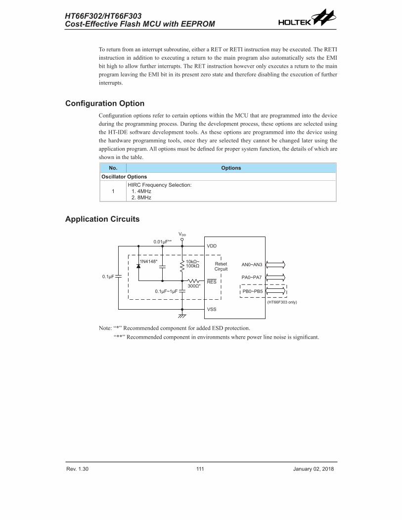
Rev. 1.30 110 ana 0 01 Rev. 1.30 111 ana 0 01
HT66F302/HT66F303Cost-Effective Flash MCU with EEPROM
HT66F302/HT66F303Cost-Effective Flash MCU with EEPROM
Toreturnfromaninterruptsubroutine,eitheraRETorRETIinstructionmaybeexecuted.TheRETIinstructioninadditiontoexecutingareturntothemainprogramalsoautomaticallysetstheEMIbithightoallowfurtherinterrupts.TheRETinstructionhoweveronlyexecutesareturntothemainprogramleavingtheEMIbitinitspresentzerostateandthereforedisablingtheexecutionoffurtherinterrupts.
Configuration OptionConfigurationoptionsrefertocertainoptionswithintheMCUthatareprogrammedintothedeviceduringtheprogrammingprocess.Duringthedevelopmentprocess,theseoptionsareselectedusingtheHT-IDEsoftwaredevelopment tools.Astheseoptionsareprogrammedintothedeviceusingthehardwareprogrammingtools,once theyareselectedtheycannotbechangedlaterusingtheapplicationprogram.Alloptionsmustbedefinedforpropersystemfunction,thedetailsofwhichareshowninthetable.
No. OptionsOscillator Options
1HIRC Feqenc Selection:
1. 4MHz. MHz
Application Circuits
VDD
VDD
RES
10kΩ~100kΩ
0.01µF**
1N4148*
VSS
0.1µF~1µF300Ω*
0.1µF
AN0~AN3
PA0~PA7
Reset Circuit
PB0~PB5
(HT66F303 only)
Note:“*”RecommendedcomponentforaddedESDprotection.“**”Recommendedcomponentinenvironmentswherepowerlinenoiseissignificant.

Rev. 1.30 11 ana 0 01 Rev. 1.30 113 ana 0 01
HT66F302/HT66F303Cost-Effective Flash MCU with EEPROM
HT66F302/HT66F303Cost-Effective Flash MCU with EEPROM
Instruction Set
IntroductionCentral to thesuccessfuloperationofanymicrocontroller is its instructionset,whichisasetofprograminstructioncodesthatdirectsthemicrocontrollertoperformcertainoperations.InthecaseofHoltekmicrocontroller,acomprehensiveandflexiblesetofover60instructionsisprovidedtoenableprogrammerstoimplementtheirapplicationwiththeminimumofprogrammingoverheads.
Foreasierunderstandingofthevariousinstructioncodes, theyhavebeensubdividedintoseveralfunctionalgroupings.
Instruction TimingMostinstructionsareimplementedwithinoneinstructioncycle.Theexceptionstothisarebranch,call,or tablereadinstructionswheretwoinstructioncyclesarerequired.Oneinstructioncycleisequalto4systemclockcycles,thereforeinthecaseofan8MHzsystemoscillator,mostinstructionswouldbeimplementedwithin0.5μsandbranchorcall instructionswouldbeimplementedwithin1μs.Although instructionswhichrequireonemorecycle to implementaregenerally limited totheJMP,CALL,RET,RETIandtablereadinstructions, it is important torealize thatanyotherinstructionswhichinvolvemanipulationoftheProgramCounterLowregisterorPCLwillalsotakeonemorecycletoimplement.AsinstructionswhichchangethecontentsofthePCLwill implyadirect jumptothatnewaddress,onemorecyclewillberequired.Examplesofsuchinstructionswouldbe“CLRPCL”or“MOVPCL,A”.Forthecaseofskipinstructions,itmustbenotedthatiftheresultofthecomparisoninvolvesaskipoperationthenthiswillalsotakeonemorecycle,ifnoskipisinvolvedthenonlyonecycleisrequired.
Moving and Transferring DataThe transferofdatawithin themicrocontrollerprogram isoneof themost frequentlyusedoperations.MakinguseofseveralkindsofMOVinstructions,datacanbetransferredfromregisterstotheAccumulatorandvice-versaaswellasbeingabletomovespecificimmediatedatadirectlyintotheAccumulator.Oneofthemostimportantdatatransferapplicationsistoreceivedatafromtheinputportsandtransferdatatotheoutputports.
Arithmetic OperationsTheabilitytoperformcertainarithmeticoperationsanddatamanipulationisanecessaryfeatureofmostmicrocontrollerapplications.WithintheHoltekmicrocontrollerinstructionsetarearangeofaddandsubtract instructionmnemonicstoenablethenecessaryarithmetictobecarriedout.Caremustbe taken toensurecorrecthandlingofcarryandborrowdatawhenresultsexceed255foradditionandless than0forsubtraction.Theincrementanddecrement instructionssuchasINC,INCA,DECandDECAprovideasimplemeansofincreasingordecreasingbyavalueofoneofthevaluesinthedestinationspecified.

Rev. 1.30 11 ana 0 01 Rev. 1.30 113 ana 0 01
HT66F302/HT66F303Cost-Effective Flash MCU with EEPROM
HT66F302/HT66F303Cost-Effective Flash MCU with EEPROM
Logical and Rotate OperationThestandardlogicaloperationssuchasAND,OR,XORandCPLallhavetheirowninstructionwithintheHoltekmicrocontroller instructionset.Aswiththecaseofmost instructionsinvolvingdatamanipulation, datamust pass through theAccumulatorwhichmay involve additionalprogrammingsteps. Inall logicaldataoperations, thezero flagmaybeset if the resultof theoperationiszero.AnotherformoflogicaldatamanipulationcomesfromtherotateinstructionssuchasRR,RL,RRCandRLCwhichprovideasimplemeansofrotatingonebitrightorleft.Differentrotateinstructionsexistdependingonprogramrequirements.Rotateinstructionsareusefulforserialportprogrammingapplicationswheredatacanberotatedfromaninternalregister intotheCarrybitfromwhereitcanbeexaminedandthenecessaryserialbitsethighorlow.Anotherapplicationwhichrotatedataoperationsareusedistoimplementmultiplicationanddivisioncalculations.
Branches and Control TransferProgrambranchingtakestheformofeitherjumpstospecifiedlocationsusingtheJMPinstructionor toa subroutineusing theCALL instruction.Theydiffer in the sense that in thecaseofasubroutinecall, theprogrammustreturn to the instruction immediatelywhenthesubroutinehasbeencarriedout.Thisisdonebyplacingareturninstruction“RET”inthesubroutinewhichwillcausetheprogramtojumpbacktotheaddressrightaftertheCALLinstruction.InthecaseofaJMPinstruction,theprogramsimplyjumpstothedesiredlocation.ThereisnorequirementtojumpbacktotheoriginaljumpingoffpointasinthecaseoftheCALLinstruction.Onespecialandextremelyusefulsetofbranchinstructionsaretheconditionalbranches.Hereadecisionisfirstmaderegardingtheconditionofacertaindatamemoryor individualbits.Dependingupon theconditions, theprogramwillcontinuewiththenextinstructionorskipoveritandjumptothefollowinginstruction.These instructionsare thekey todecisionmakingandbranchingwithin theprogramperhapsdeterminedbytheconditionofcertaininputswitchesorbytheconditionofinternaldatabits.
Bit OperationsTheabilitytoprovidesinglebitoperationsonDataMemoryisanextremelyflexiblefeatureofallHoltekmicrocontrollers.Thisfeature isespeciallyusefulforoutputportbitprogrammingwhereindividualbitsorportpinscanbedirectlysethighorlowusingeitherthe“SET[m].i”or“CLR[m].i”instructionsrespectively.Thefeatureremovestheneedforprogrammerstofirstreadthe8-bitoutputport,manipulatetheinputdatatoensurethatotherbitsarenotchangedandthenoutputtheportwiththecorrectnewdata.Thisread-modify-writeprocessistakencareofautomaticallywhenthesebitoperationinstructionsareused.
Table Read OperationsDatastorage isnormally implementedbyusing registers.However,whenworkingwith largeamountsoffixeddata, thevolumeinvolvedoftenmakesit inconvenienttostorethefixeddataintheDataMemory.Toovercomethisproblem,HoltekmicrocontrollersallowanareaofProgramMemorytobesetupasatablewheredatacanbedirectlystored.Asetofeasytouseinstructionsprovides themeansbywhich this fixeddatacanbereferencedandretrievedfromtheProgramMemory.
Other OperationsInaddition to theabovefunctional instructions,a rangeofother instructionsalsoexistsuchasthe“HALT”instructionforPower-downoperationsand instructions tocontrol theoperationoftheWatchdogTimerfor reliableprogramoperationsunderextremeelectricorelectromagneticenvironments.Fortheirrelevantoperations,refertothefunctionalrelatedsections.
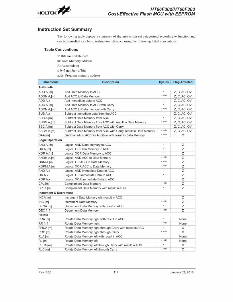
Rev. 1.30 114 ana 0 01 Rev. 1.30 115 ana 0 01
HT66F302/HT66F303Cost-Effective Flash MCU with EEPROM
HT66F302/HT66F303Cost-Effective Flash MCU with EEPROM
Instruction Set SummaryThefollowingtabledepictsasummaryoftheinstructionsetcategorisedaccordingtofunctionandcanbeconsultedasabasicinstructionreferenceusingthefollowinglistedconventions.
Table Conventionsx:Bitsimmediatedatam:DataMemoryaddressA:Accumulatori:0~7numberofbitsaddr:Programmemoryaddress
Mnemonic Description Cycles Flag AffectedArithmeticADD A[m] Add Data Memo to ACC 1 Z C AC OVADDM A[m] Add ACC to Data Memo 1Note Z C AC OVADD Ax Add immediate data to ACC 1 Z C AC OVADC A[m] Add Data Memo to ACC with Ca 1 Z C AC OVADCM A[m] Add ACC to Data memo with Ca 1Note Z C AC OVSUB Ax Sbtact immediate data fom the ACC 1 Z C AC OVSUB A[m] Sbtact Data Memo fom ACC 1 Z C AC OVSUBM A[m] Sbtact Data Memo fom ACC with eslt in Data Memo 1Note Z C AC OVSBC A[m] Sbtact Data Memo fom ACC with Ca 1 Z C AC OVSBCM A[m] Sbtact Data Memo fom ACC with Ca eslt in Data Memo 1Note Z C AC OVDAA [m] Decimal adjst ACC fo Addition with eslt in Data Memo 1Note CLogic OperationAND A[m] Logical AND Data Memo to ACC 1 ZOR A[m] Logical OR Data Memo to ACC 1 ZXOR A[m] Logical XOR Data Memo to ACC 1 ZANDM A[m] Logical AND ACC to Data Memo 1Note ZORM A[m] Logical OR ACC to Data Memo 1Note ZXORM A[m] Logical XOR ACC to Data Memo 1Note ZAND Ax Logical AND immediate Data to ACC 1 ZOR Ax Logical OR immediate Data to ACC 1 ZXOR Ax Logical XOR immediate Data to ACC 1 ZCPL [m] Complement Data Memo 1Note ZCPLA [m] Complement Data Memo with eslt in ACC 1 ZIncrement & DecrementINCA [m] Incement Data Memo with eslt in ACC 1 ZINC [m] Incement Data Memo 1Note ZDECA [m] Decement Data Memo with eslt in ACC 1 ZDEC [m] Decement Data Memo 1Note ZRotateRRA [m] Rotate Data Memo ight with eslt in ACC 1 NoneRR [m] Rotate Data Memo ight 1Note NoneRRCA [m] Rotate Data Memo ight thogh Ca with eslt in ACC 1 CRRC [m] Rotate Data Memo ight thogh Ca 1Note CRLA [m] Rotate Data Memo left with eslt in ACC 1 NoneRL [m] Rotate Data Memo left 1Note NoneRLCA [m] Rotate Data Memo left thogh Ca with eslt in ACC 1 CRLC [m] Rotate Data Memo left thogh Ca 1Note C
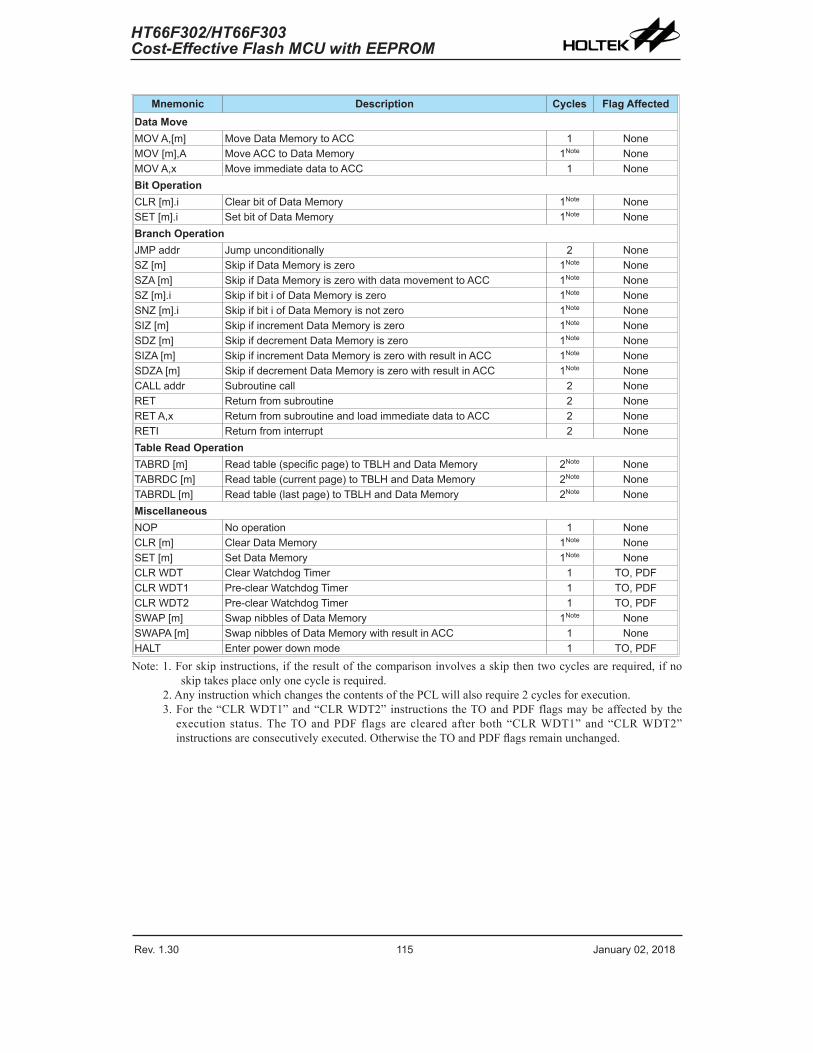
Rev. 1.30 114 ana 0 01 Rev. 1.30 115 ana 0 01
HT66F302/HT66F303Cost-Effective Flash MCU with EEPROM
HT66F302/HT66F303Cost-Effective Flash MCU with EEPROM
Mnemonic Description Cycles Flag AffectedData MoveMOV A[m] Move Data Memo to ACC 1 NoneMOV [m]A Move ACC to Data Memo 1Note NoneMOV Ax Move immediate data to ACC 1 NoneBit OperationCLR [m].i Clea bit of Data Memo 1Note NoneSET [m].i Set bit of Data Memo 1Note NoneBranch OperationMP add mp nconditionall NoneSZ [m] Skip if Data Memo is zeo 1Note NoneSZA [m] Skip if Data Memo is zeo with data movement to ACC 1Note NoneSZ [m].i Skip if bit i of Data Memo is zeo 1Note NoneSNZ [m].i Skip if bit i of Data Memo is not zeo 1Note NoneSIZ [m] Skip if incement Data Memo is zeo 1Note NoneSDZ [m] Skip if decement Data Memo is zeo 1Note NoneSIZA [m] Skip if incement Data Memo is zeo with eslt in ACC 1Note NoneSDZA [m] Skip if decement Data Memo is zeo with eslt in ACC 1Note NoneCALL add Sbotine call NoneRET Retn fom sbotine NoneRET Ax Retn fom sbotine and load immediate data to ACC NoneRETI Retn fom intept NoneTable Read OperationTABRD [m] Read table (specific page) to TBLH and Data Memory Note NoneTABRDC [m] Read table (cent page) to TBLH and Data Memo Note NoneTABRDL [m] Read table (last page) to TBLH and Data Memo Note NoneMiscellaneousNOP No opeation 1 NoneCLR [m] Clea Data Memo 1Note NoneSET [m] Set Data Memo 1Note NoneCLR WDT Clea Watchdog Time 1 TO PDFCLR WDT1 Pe-clea Watchdog Time 1 TO PDFCLR WDT Pe-clea Watchdog Time 1 TO PDFSWAP [m] Swap nibbles of Data Memo 1Note NoneSWAPA [m] Swap nibbles of Data Memo with eslt in ACC 1 NoneHALT Ente powe down mode 1 TO PDF
Note:1.Forskipinstructions,iftheresultofthecomparisoninvolvesaskipthentwocyclesarerequired,ifnoskiptakesplaceonlyonecycleisrequired.
2.AnyinstructionwhichchangesthecontentsofthePCLwillalsorequire2cyclesforexecution.3.For the“CLRWDT1”and“CLRWDT2”instructionstheTOandPDFflagsmaybeaffectedbytheexecution status.TheTOandPDFflagsareclearedafterboth“CLRWDT1”and“CLRWDT2”instructionsareconsecutivelyexecuted.OtherwisetheTOandPDFflagsremainunchanged.

Rev. 1.30 116 ana 0 01 Rev. 1.30 117 ana 0 01
HT66F302/HT66F303Cost-Effective Flash MCU with EEPROM
HT66F302/HT66F303Cost-Effective Flash MCU with EEPROM
Instruction Definition
ADC A,[m] AddDataMemorytoACCwithCarryDescription ThecontentsofthespecifiedDataMemory,Accumulatorandthecarryflagareadded. TheresultisstoredintheAccumulator.Operation ACC←ACC+[m]+CAffectedflag(s) OV,Z,AC,C
ADCM A,[m] AddACCtoDataMemorywithCarryDescription ThecontentsofthespecifiedDataMemory,Accumulatorandthecarryflagareadded. TheresultisstoredinthespecifiedDataMemory.Operation [m]←ACC+[m]+CAffectedflag(s) OV,Z,AC,C
ADD A,[m] AddDataMemorytoACCDescription ThecontentsofthespecifiedDataMemoryandtheAccumulatorareadded. TheresultisstoredintheAccumulator.Operation ACC←ACC+[m]Affectedflag(s) OV,Z,AC,C
ADD A,x AddimmediatedatatoACCDescription ThecontentsoftheAccumulatorandthespecifiedimmediatedataareadded. TheresultisstoredintheAccumulator.Operation ACC←ACC+xAffectedflag(s) OV,Z,AC,C
ADDM A,[m] AddACCtoDataMemoryDescription ThecontentsofthespecifiedDataMemoryandtheAccumulatorareadded. TheresultisstoredinthespecifiedDataMemory.Operation [m]←ACC+[m]Affectedflag(s) OV,Z,AC,C
AND A,[m] LogicalANDDataMemorytoACCDescription DataintheAccumulatorandthespecifiedDataMemoryperformabitwiselogicalAND operation.TheresultisstoredintheAccumulator.Operation ACC←ACC″AND″[m]Affectedflag(s) Z
AND A,x LogicalANDimmediatedatatoACCDescription DataintheAccumulatorandthespecifiedimmediatedataperformabitwiselogicalAND operation.TheresultisstoredintheAccumulator.Operation ACC←ACC″AND″xAffectedflag(s) Z
ANDM A,[m] LogicalANDACCtoDataMemoryDescription DatainthespecifiedDataMemoryandtheAccumulatorperformabitwiselogicalAND operation.TheresultisstoredintheDataMemory.Operation [m]←ACC″AND″[m]Affectedflag(s) Z

Rev. 1.30 116 ana 0 01 Rev. 1.30 117 ana 0 01
HT66F302/HT66F303Cost-Effective Flash MCU with EEPROM
HT66F302/HT66F303Cost-Effective Flash MCU with EEPROM
CALL addr SubroutinecallDescription Unconditionallycallsasubroutineatthespecifiedaddress.TheProgramCounterthen incrementsby1toobtaintheaddressofthenextinstructionwhichisthenpushedontothe stack.Thespecifiedaddressisthenloadedandtheprogramcontinuesexecutionfromthis newaddress.Asthisinstructionrequiresanadditionaloperation,itisatwocycleinstruction.Operation Stack←ProgramCounter+1 ProgramCounter←addrAffectedflag(s) None
CLR [m] ClearDataMemoryDescription EachbitofthespecifiedDataMemoryisclearedto0.Operation [m]←00HAffectedflag(s) None
CLR [m].i ClearbitofDataMemoryDescription BitiofthespecifiedDataMemoryisclearedto0.Operation [m].i←0Affectedflag(s) None
CLR WDT ClearWatchdogTimerDescription TheTO,PDFflagsandtheWDTareallcleared.Operation WDTcleared TO←0 PDF←0Affectedflag(s) TO,PDF
CLR WDT1 Pre-clearWatchdogTimerDescription TheTO,PDFflagsandtheWDTareallcleared.Notethatthisinstructionworksin conjunctionwithCLRWDT2andmustbeexecutedalternatelywithCLRWDT2tohave effect.RepetitivelyexecutingthisinstructionwithoutalternatelyexecutingCLRWDT2will havenoeffect.Operation WDTcleared TO←0 PDF←0Affectedflag(s) TO,PDF
CLR WDT2 Pre-clearWatchdogTimerDescription TheTO,PDFflagsandtheWDTareallcleared.Notethatthisinstructionworksinconjunction withCLRWDT1andmustbeexecutedalternatelywithCLRWDT1tohaveeffect. RepetitivelyexecutingthisinstructionwithoutalternatelyexecutingCLRWDT1willhaveno effect.Operation WDTcleared TO←0 PDF←0Affectedflag(s) TO,PDF
CPL [m] ComplementDataMemoryDescription EachbitofthespecifiedDataMemoryislogicallycomplemented(1′scomplement).Bitswhich previouslycontaineda1arechangedto0andviceversa.Operation [m]←[m]Affectedflag(s) Z

Rev. 1.30 11 ana 0 01 Rev. 1.30 119 ana 0 01
HT66F302/HT66F303Cost-Effective Flash MCU with EEPROM
HT66F302/HT66F303Cost-Effective Flash MCU with EEPROM
CPLA [m] ComplementDataMemorywithresultinACCDescription EachbitofthespecifiedDataMemoryislogicallycomplemented(1′scomplement).Bitswhich previouslycontaineda1arechangedto0andviceversa.Thecomplementedresultisstoredin theAccumulatorandthecontentsoftheDataMemoryremainunchanged.Operation ACC←[m]Affectedflag(s) Z
DAA [m] Decimal-AdjustACCforadditionwithresultinDataMemoryDescription ConvertthecontentsoftheAccumulatorvaluetoaBCD(BinaryCodedDecimal)value resultingfromthepreviousadditionoftwoBCDvariables.Ifthelownibbleisgreaterthan9 orifACflagisset,thenavalueof6willbeaddedtothelownibble.Otherwisethelownibble remainsunchanged.Ifthehighnibbleisgreaterthan9oriftheCflagisset,thenavalueof6 willbeaddedtothehighnibble.Essentially,thedecimalconversionisperformedbyadding 00H,06H,60Hor66HdependingontheAccumulatorandflagconditions.OnlytheCflag maybeaffectedbythisinstructionwhichindicatesthatiftheoriginalBCDsumisgreaterthan 100,itallowsmultipleprecisiondecimaladdition.Operation [m]←ACC+00Hor [m]←ACC+06Hor [m]←ACC+60Hor [m]←ACC+66HAffectedflag(s) C
DEC [m] DecrementDataMemoryDescription DatainthespecifiedDataMemoryisdecrementedby1.Operation [m]←[m]−1Affectedflag(s) Z
DECA [m] DecrementDataMemorywithresultinACCDescription DatainthespecifiedDataMemoryisdecrementedby1.Theresultisstoredinthe Accumulator.ThecontentsoftheDataMemoryremainunchanged.Operation ACC←[m]−1Affectedflag(s) Z
HALT EnterpowerdownmodeDescription Thisinstructionstopstheprogramexecutionandturnsoffthesystemclock.Thecontentsof theDataMemoryandregistersareretained.TheWDTandprescalerarecleared.Thepower downflagPDFissetandtheWDTtime-outflagTOiscleared.Operation TO←0 PDF←1Affectedflag(s) TO,PDF
INC [m] IncrementDataMemoryDescription DatainthespecifiedDataMemoryisincrementedby1.Operation [m]←[m]+1Affectedflag(s) Z
INCA [m] IncrementDataMemorywithresultinACCDescription DatainthespecifiedDataMemoryisincrementedby1.TheresultisstoredintheAccumulator. ThecontentsoftheDataMemoryremainunchanged.Operation ACC←[m]+1Affectedflag(s) Z

Rev. 1.30 11 ana 0 01 Rev. 1.30 119 ana 0 01
HT66F302/HT66F303Cost-Effective Flash MCU with EEPROM
HT66F302/HT66F303Cost-Effective Flash MCU with EEPROM
JMP addr JumpunconditionallyDescription ThecontentsoftheProgramCounterarereplacedwiththespecifiedaddress.Program executionthencontinuesfromthisnewaddress.Asthisrequirestheinsertionofadummy instructionwhilethenewaddressisloaded,itisatwocycleinstruction.Operation ProgramCounter←addrAffectedflag(s) None
MOV A,[m] MoveDataMemorytoACCDescription ThecontentsofthespecifiedDataMemoryarecopiedtotheAccumulator.Operation ACC←[m]Affectedflag(s) None
MOV A,x MoveimmediatedatatoACCDescription TheimmediatedataspecifiedisloadedintotheAccumulator.Operation ACC←xAffectedflag(s) None
MOV [m],A MoveACCtoDataMemoryDescription ThecontentsoftheAccumulatorarecopiedtothespecifiedDataMemory.Operation [m]←ACCAffectedflag(s) None
NOP NooperationDescription Nooperationisperformed.Executioncontinueswiththenextinstruction.Operation NooperationAffectedflag(s) None
OR A,[m] LogicalORDataMemorytoACCDescription DataintheAccumulatorandthespecifiedDataMemoryperformabitwise logicalORoperation.TheresultisstoredintheAccumulator.Operation ACC←ACC″OR″[m]Affectedflag(s) Z
OR A,x LogicalORimmediatedatatoACCDescription DataintheAccumulatorandthespecifiedimmediatedataperformabitwiselogicalOR operation.TheresultisstoredintheAccumulator.Operation ACC←ACC″OR″xAffectedflag(s) Z
ORM A,[m] LogicalORACCtoDataMemoryDescription DatainthespecifiedDataMemoryandtheAccumulatorperformabitwiselogicalOR operation.TheresultisstoredintheDataMemory.Operation [m]←ACC″OR″[m]Affectedflag(s) Z
RET ReturnfromsubroutineDescription TheProgramCounterisrestoredfromthestack.Programexecutioncontinuesattherestored address.Operation ProgramCounter←StackAffectedflag(s) None

Rev. 1.30 10 ana 0 01 Rev. 1.30 11 ana 0 01
HT66F302/HT66F303Cost-Effective Flash MCU with EEPROM
HT66F302/HT66F303Cost-Effective Flash MCU with EEPROM
RET A,x ReturnfromsubroutineandloadimmediatedatatoACCDescription TheProgramCounterisrestoredfromthestackandtheAccumulatorloadedwiththespecified immediatedata.Programexecutioncontinuesattherestoredaddress.Operation ProgramCounter←Stack ACC←xAffectedflag(s) None
RETI ReturnfrominterruptDescription TheProgramCounterisrestoredfromthestackandtheinterruptsarere-enabledbysettingthe EMIbit.EMIisthemasterinterruptglobalenablebit.Ifaninterruptwaspendingwhenthe RETIinstructionisexecuted,thependingInterruptroutinewillbeprocessedbeforereturning tothemainprogram.Operation ProgramCounter←Stack EMI←1Affectedflag(s) None
RL [m] RotateDataMemoryleftDescription ThecontentsofthespecifiedDataMemoryarerotatedleftby1bitwithbit7rotatedintobit0.Operation [m].(i+1)←[m].i;(i=0~6) [m].0←[m].7Affectedflag(s) None
RLA [m] RotateDataMemoryleftwithresultinACCDescription ThecontentsofthespecifiedDataMemoryarerotatedleftby1bitwithbit7rotatedintobit0. TherotatedresultisstoredintheAccumulatorandthecontentsoftheDataMemoryremain unchanged.Operation ACC.(i+1)←[m].i;(i=0~6) ACC.0←[m].7Affectedflag(s) None
RLC [m] RotateDataMemoryleftthroughCarryDescription ThecontentsofthespecifiedDataMemoryandthecarryflagarerotatedleftby1bit.Bit7 replacestheCarrybitandtheoriginalcarryflagisrotatedintobit0.Operation [m].(i+1)←[m].i;(i=0~6) [m].0←C C←[m].7Affectedflag(s) C
RLCA [m] RotateDataMemoryleftthroughCarrywithresultinACCDescription DatainthespecifiedDataMemoryandthecarryflagarerotatedleftby1bit.Bit7replacesthe Carrybitandtheoriginalcarryflagisrotatedintothebit0.Therotatedresultisstoredinthe AccumulatorandthecontentsoftheDataMemoryremainunchanged.Operation ACC.(i+1)←[m].i;(i=0~6) ACC.0←C C←[m].7Affectedflag(s) C
RR [m] RotateDataMemoryrightDescription ThecontentsofthespecifiedDataMemoryarerotatedrightby1bitwithbit0rotatedintobit7.Operation [m].i←[m].(i+1);(i=0~6) [m].7←[m].0Affectedflag(s) None

Rev. 1.30 10 ana 0 01 Rev. 1.30 11 ana 0 01
HT66F302/HT66F303Cost-Effective Flash MCU with EEPROM
HT66F302/HT66F303Cost-Effective Flash MCU with EEPROM
RRA [m] RotateDataMemoryrightwithresultinACCDescription DatainthespecifiedDataMemoryisrotatedrightby1bitwithbit0rotatedintobit7. TherotatedresultisstoredintheAccumulatorandthecontentsofthe DataMemoryremainunchanged.Operation ACC.i←[m].(i+1);(i=0~6) ACC.7←[m].0Affectedflag(s) None
RRC [m] RotateDataMemoryrightthroughCarryDescription ThecontentsofthespecifiedDataMemoryandthecarryflagarerotatedrightby1bit.Bit0 replacestheCarrybitandtheoriginalcarryflagisrotatedintobit7.Operation [m].i←[m].(i+1);(i=0~6) [m].7←C C←[m].0Affectedflag(s) C
RRCA [m] RotateDataMemoryrightthroughCarrywithresultinACCDescription DatainthespecifiedDataMemoryandthecarryflagarerotatedrightby1bit.Bit0replaces theCarrybitandtheoriginalcarryflagisrotatedintobit7.Therotatedresultisstoredinthe AccumulatorandthecontentsoftheDataMemoryremainunchanged.Operation ACC.i←[m].(i+1);(i=0~6) ACC.7←C C←[m].0Affectedflag(s) C
SBC A,[m] SubtractDataMemoryfromACCwithCarryDescription ThecontentsofthespecifiedDataMemoryandthecomplementofthecarryflagare subtractedfromtheAccumulator.TheresultisstoredintheAccumulator.Notethatifthe resultofsubtractionisnegative,theCflagwillbeclearedto0,otherwiseiftheresultis positiveorzero,theCflagwillbesetto1.Operation ACC←ACC−[m]−CAffectedflag(s) OV,Z,AC,C
SBCM A,[m] SubtractDataMemoryfromACCwithCarryandresultinDataMemoryDescription ThecontentsofthespecifiedDataMemoryandthecomplementofthecarryflagare subtractedfromtheAccumulator.TheresultisstoredintheDataMemory.Notethatifthe resultofsubtractionisnegative,theCflagwillbeclearedto0,otherwiseiftheresultis positiveorzero,theCflagwillbesetto1.Operation [m]←ACC−[m]−CAffectedflag(s) OV,Z,AC,C
SDZ [m] SkipifdecrementDataMemoryis0Description ThecontentsofthespecifiedDataMemoryarefirstdecrementedby1.Iftheresultis0the followinginstructionisskipped.Asthisrequirestheinsertionofadummyinstructionwhile thenextinstructionisfetched,itisatwocycleinstruction.Iftheresultisnot0theprogram proceedswiththefollowinginstruction.Operation [m]←[m]−1 Skipif[m]=0Affectedflag(s) None

Rev. 1.30 1 ana 0 01 Rev. 1.30 13 ana 0 01
HT66F302/HT66F303Cost-Effective Flash MCU with EEPROM
HT66F302/HT66F303Cost-Effective Flash MCU with EEPROM
SDZA [m] SkipifdecrementDataMemoryiszerowithresultinACCDescription ThecontentsofthespecifiedDataMemoryarefirstdecrementedby1.Iftheresultis0,the followinginstructionisskipped.TheresultisstoredintheAccumulatorbutthespecified DataMemorycontentsremainunchanged.Asthisrequirestheinsertionofadummy instructionwhilethenextinstructionisfetched,itisatwocycleinstruction.Iftheresultisnot0, theprogramproceedswiththefollowinginstruction.Operation ACC←[m]−1 SkipifACC=0Affectedflag(s) None
SET [m] SetDataMemoryDescription EachbitofthespecifiedDataMemoryissetto1.Operation [m]←FFHAffectedflag(s) None
SET [m].i SetbitofDataMemoryDescription BitiofthespecifiedDataMemoryissetto1.Operation [m].i←1Affectedflag(s) None
SIZ [m] SkipifincrementDataMemoryis0Description ThecontentsofthespecifiedDataMemoryarefirstincrementedby1.Iftheresultis0,the followinginstructionisskipped.Asthisrequirestheinsertionofadummyinstructionwhile thenextinstructionisfetched,itisatwocycleinstruction.Iftheresultisnot0theprogram proceedswiththefollowinginstruction.Operation [m]←[m]+1 Skipif[m]=0Affectedflag(s) None
SIZA [m] SkipifincrementDataMemoryiszerowithresultinACCDescription ThecontentsofthespecifiedDataMemoryarefirstincrementedby1.Iftheresultis0,the followinginstructionisskipped.TheresultisstoredintheAccumulatorbutthespecified DataMemorycontentsremainunchanged.Asthisrequirestheinsertionofadummy instructionwhilethenextinstructionisfetched,itisatwocycleinstruction.Iftheresultisnot 0theprogramproceedswiththefollowinginstruction.Operation ACC←[m]+1 SkipifACC=0Affectedflag(s) None
SNZ [m].i SkipifbitiofDataMemoryisnot0Description IfbitiofthespecifiedDataMemoryisnot0,thefollowinginstructionisskipped.Asthis requirestheinsertionofadummyinstructionwhilethenextinstructionisfetched,itisatwo cycleinstruction.Iftheresultis0theprogramproceedswiththefollowinginstruction.Operation Skipif[m].i≠0Affectedflag(s) None
SUB A,[m] SubtractDataMemoryfromACCDescription ThespecifiedDataMemoryissubtractedfromthecontentsoftheAccumulator.Theresultis storedintheAccumulator.Notethatiftheresultofsubtractionisnegative,theCflagwillbe clearedto0,otherwiseiftheresultispositiveorzero,theCflagwillbesetto1.Operation ACC←ACC−[m]Affectedflag(s) OV,Z,AC,C

Rev. 1.30 1 ana 0 01 Rev. 1.30 13 ana 0 01
HT66F302/HT66F303Cost-Effective Flash MCU with EEPROM
HT66F302/HT66F303Cost-Effective Flash MCU with EEPROM
SUBM A,[m] SubtractDataMemoryfromACCwithresultinDataMemoryDescription ThespecifiedDataMemoryissubtractedfromthecontentsoftheAccumulator.Theresultis storedintheDataMemory.Notethatiftheresultofsubtractionisnegative,theCflagwillbe clearedto0,otherwiseiftheresultispositiveorzero,theCflagwillbesetto1.Operation [m]←ACC−[m]Affectedflag(s) OV,Z,AC,C
SUB A,x SubtractimmediatedatafromACCDescription TheimmediatedataspecifiedbythecodeissubtractedfromthecontentsoftheAccumulator. TheresultisstoredintheAccumulator.Notethatiftheresultofsubtractionisnegative,theC flagwillbeclearedto0,otherwiseiftheresultispositiveorzero,theCflagwillbesetto1.Operation ACC←ACC−xAffectedflag(s) OV,Z,AC,C
SWAP [m] SwapnibblesofDataMemoryDescription Thelow-orderandhigh-ordernibblesofthespecifiedDataMemoryareinterchanged.Operation [m].3~[m].0↔[m].7~[m].4Affectedflag(s) None
SWAPA [m] SwapnibblesofDataMemorywithresultinACCDescription Thelow-orderandhigh-ordernibblesofthespecifiedDataMemoryareinterchanged.The resultisstoredintheAccumulator.ThecontentsoftheDataMemoryremainunchanged.Operation ACC.3~ACC.0←[m].7~[m].4 ACC.7~ACC.4←[m].3~[m].0Affectedflag(s) None
SZ [m] SkipifDataMemoryis0Description IfthecontentsofthespecifiedDataMemoryis0,thefollowinginstructionisskipped.Asthis requirestheinsertionofadummyinstructionwhilethenextinstructionisfetched,itisatwo cycleinstruction.Iftheresultisnot0theprogramproceedswiththefollowinginstruction.Operation Skipif[m]=0Affectedflag(s) None
SZA [m] SkipifDataMemoryis0withdatamovementtoACCDescription ThecontentsofthespecifiedDataMemoryarecopiedtotheAccumulator.Ifthevalueiszero, thefollowinginstructionisskipped.Asthisrequirestheinsertionofadummyinstruction whilethenextinstructionisfetched,itisatwocycleinstruction.Iftheresultisnot0the programproceedswiththefollowinginstruction.Operation ACC←[m] Skipif[m]=0Affectedflag(s) None
SZ [m].i SkipifbitiofDataMemoryis0Description IfbitiofthespecifiedDataMemoryis0,thefollowinginstructionisskipped.Asthisrequires theinsertionofadummyinstructionwhilethenextinstructionisfetched,itisatwocycle instruction.Iftheresultisnot0,theprogramproceedswiththefollowinginstruction.Operation Skipif[m].i=0Affectedflag(s) None

Rev. 1.30 14 ana 0 01 Rev. 1.30 15 ana 0 01
HT66F302/HT66F303Cost-Effective Flash MCU with EEPROM
HT66F302/HT66F303Cost-Effective Flash MCU with EEPROM
TABRD [m] Readtable(specificpage)toTBLHandDataMemoryDescription Thelowbyteoftheprogramcode(specificpage)addressedbythetablepointerpair (TBHPandTBLP)ismovedtothespecifiedDataMemoryandthehighbytemovedtoTBLH.Operation [m]←programcode(lowbyte) TBLH←programcode(highbyte)Affectedflag(s) None
TABRDC [m] Readtable(currentpage)toTBLHandDataMemoryDescription Thelowbyteoftheprogramcode(currentpage)addressedbythetablepointer(TBLP)is movedtothespecifiedDataMemoryandthehighbytemovedtoTBLH.Operation [m]←programcode(lowbyte) TBLH←programcode(highbyte)Affectedflag(s) None
TABRDL [m] Readtable(lastpage)toTBLHandDataMemoryDescription Thelowbyteoftheprogramcode(lastpage)addressedbythetablepointer(TBLP)ismoved tothespecifiedDataMemoryandthehighbytemovedtoTBLH.Operation [m]←programcode(lowbyte) TBLH←programcode(highbyte)Affectedflag(s) None
XOR A,[m] LogicalXORDataMemorytoACCDescription DataintheAccumulatorandthespecifiedDataMemoryperformabitwiselogicalXOR operation.TheresultisstoredintheAccumulator.Operation ACC←ACC″XOR″[m]Affectedflag(s) Z
XORM A,[m] LogicalXORACCtoDataMemoryDescription DatainthespecifiedDataMemoryandtheAccumulatorperformabitwiselogicalXOR operation.TheresultisstoredintheDataMemory.Operation [m]←ACC″XOR″[m]Affectedflag(s) Z
XOR A,x LogicalXORimmediatedatatoACCDescription DataintheAccumulatorandthespecifiedimmediatedataperformabitwiselogicalXOR operation.TheresultisstoredintheAccumulator.Operation ACC←ACC″XOR″xAffectedflag(s) Z

Rev. 1.30 14 ana 0 01 Rev. 1.30 15 ana 0 01
HT66F302/HT66F303Cost-Effective Flash MCU with EEPROM
HT66F302/HT66F303Cost-Effective Flash MCU with EEPROM
Package Information
Note that thepackage informationprovidedhere is for consultationpurposesonly.As thisinformationmaybeupdatedatregularintervalsusersareremindedtoconsulttheHoltekwebsiteforthelatestversionofthePackage/CartonInformation.
Additionalsupplementaryinformationwithregardtopackagingislistedbelow.Clickontherelevantsectiontobetransferredtotherelevantwebsitepage.
• FurtherPackageInformation(includeOutlineDimensions,ProductTapeandReelSpecifications)
• PackingMeterialsInformation
• Cartoninformation

Rev. 1.30 16 ana 0 01 Rev. 1.30 17 ana 0 01
HT66F302/HT66F303Cost-Effective Flash MCU with EEPROM
HT66F302/HT66F303Cost-Effective Flash MCU with EEPROM
8-pin SOP (150mil) Outline Dimensions
SymbolDimensions in inch
Min. Nom. Max.A — 0.36 BSC —B — 0.154 BSC —C 0.01 — 0.00C′ — 0.193 BSC —D — — 0.069E — 0.050 BSC —F 0.004 — 0.010G 0.016 — 0.050H 0.004 — 0.010α 0° — °
SymbolDimensions in mm
Min. Nom. Max.A — 6.00 BSC —B — 3.90 BSC —C 0.31 — 0.51C′ — 4.90 BSC —D — — 1.75E — 1.7 BSC —F 0.10 — 0.5G 0.40 — 1.7H 0.10 — 0.5α 0° — °

Rev. 1.30 16 ana 0 01 Rev. 1.30 17 ana 0 01
HT66F302/HT66F303Cost-Effective Flash MCU with EEPROM
HT66F302/HT66F303Cost-Effective Flash MCU with EEPROM
10-pin SOP (150mil) Outline Dimensions
SymbolDimensions in inch
Min. Nom. Max.A — 0.36 BSC —B — 0.154 BSC —C 0.01 — 0.01C′ — 0.193 BSC —D — — 0.069E — 0.039 BSC —F 0.004 — 0.010G 0.016 — 0.050H 0.004 — 0.010α 0° — °
SymbolDimensions in mm
Min. Nom. Max.A —F 6.00 BSC —B — 3.90 BSC —C 0.30 — 0.45C′ — 4.90 BSC —D — — 1.75E — 1.00 BSC —F 0.10 — 0.5G 0.40 — 1.7H 0.10 — 0.5α 0° — °

Rev. 1.30 1 ana 0 01 Rev. 1.30 19 ana 0 01
HT66F302/HT66F303Cost-Effective Flash MCU with EEPROM
HT66F302/HT66F303Cost-Effective Flash MCU with EEPROM
16-pin NSOP (150mil) Outline Dimensions
SymbolDimensions in inch
Min. Nom. Max.A — 0.36 BSC —B — 0.154 BSC —C 0.01 — 0.00C’ — 0.390 BSC —D — — 0.069E — 0.050 BSC —F 0.004 — 0.010G 0.016 — 0.050H 0.004 — 0.010α 0° — °
SymbolDimensions in mm
Min. Nom. Max.A — 6.0 BSC —B — 3.9 BSC —C 0.31 — 0.51C’ — 9.9 BSC —D — — 1.75E — 1.7 BSC —F 0.10 — 0.5G 0.40 — 1.7H 0.10 — 0.5α 0° — °

Rev. 1.30 1 ana 0 01 Rev. 1.30 19 ana 0 01
HT66F302/HT66F303Cost-Effective Flash MCU with EEPROM
HT66F302/HT66F303Cost-Effective Flash MCU with EEPROM
Copight© 01 b HOLTEK SEMICONDUCTOR INC.
The infomation appeaing in this Data Sheet is believed to be accate at the time of pblication. Howeve Holtek assmes no esponsibilit aising fom the se of the specifications described. The applications mentioned herein are used solely fo the ppose of illstation and Holtek makes no waant o epesentation that sch applications will be sitable withot fthe modification no ecommends the se of its podcts fo application that ma pesent a isk to hman life de to malfnction o othewise. Holtek's podcts ae not athoized fo se as citical components in life sppot devices o sstems. Holtek eseves the ight to alte its products without prior notification. For the most up-to-date information, please visit o web site at http://www.holtek.com.tw.


![How to RESET I-PIN (Internet Pin) in CRA-NSDL · NPS SOP to reset PASSWORD [I-PIN (Internet Pin)] in CRA-NSDL website NPS Section, DAT Phone: 0413 - 2213313. Ext – 227 Email: DATNPS.PON@NIC.IN](https://img.dokumen.tips/doc/110x75/5e73a1e47b4cd459b11a6d0d/how-to-reset-i-pin-internet-pin-in-cra-nsdl-nps-sop-to-reset-password-i-pin-internet.jpg)

