Embed Size (px)
Citation preview

NASA / TM--2000-208876
Correlation Between Material Properties of
Ferroelectric Thin Films and Design Parameters
for Microwave Device Appl.ications: Modeling
Examples and Experimental Verification
F61ix A. Miranda and Fred W. Van Keuls
Glenn Research Center, Cleveland, Ohio
Guru Subramanyam
University of Dayton, Dayton, Ohio
Carl H. Mueller and Robert R. Romanofsky
Glenn Research Center, Cleveland, Ohio
Gerardo Rosado
University of Puerto Rico, Humacao, Puerto Rico
April 2000
https://ntrs.nasa.gov/search.jsp?R=20000053481 2018-06-08T10:17:55+00:00Z

The NASA STI Program Office... in Profile
Since its founding, NASA has been dedicated to
the advancement of aeronautics and spacescience. The NASA Scientific and Technical
Information (STI) Program Office plays a key partin helping NASA maintain this important role.
The NASA STI Program Office is operated byLangley Research Center, the Lead Center forNASA's scientific and technical information. The
NASA STI Program Office provides access to the
NASA STI Database, the largest collection ofaeronautical and space science STI in the world.The Program Office is also NASA's institutional
mechanism for disseminating the results of its
research and development activities. These results
are published by NASA in the NASA STI Report
Series, which includes the following report types:
TECHNICAL PUBLICATION. Reports of
completed research or a major significantphase of research that present the results ofNASA programs and include extensive data
or theoretical analysis. Includes compilationsof significant scientific and technical data and
information deemed to be of continuing
reference value. NASA's counterpart of peer-reviewed formal professional papers but
has less stringent limitations on manuscriptlength and extent of graphic presentations.
TECHNICAL MEMORANDUM. Scientific
and technical findings that are preliminary orof specialized interest, e.g., quick release
reports, working papers, and bibliographiesthat contain minimal annotation. Does not
contain extensive analysis.
CONTRACTOR REPORT. Scientific and
technical findings by NASA-sponsoredcontractors and grantees.
CONFERENCE PUBLICATION. Collected
papers from scientific and technical
conferences, symposia, seminars, or other
meetings sponsored or cosponsored byNASA.
SPECIAL PUBLICATION. Scientific,technical, or historical information from
NASA programs, projects, and missions,
often concerned with subjects havingsubstantial public interest.
TECHNICAL TRANSLATION. English-language translations of foreign scientificand technical material pertinent to NASA'smission.
Specialized services that complement the STI
Program Office's diverse offerings includecreating custom thesauri, building customized
data bases, organizing and publishing researchresults.., even providing videos.
For more information about the NASA STI
Program Office, see the following:
Access the NASA STI Program Home Pageat http'.//www.sti.nasa.gov
E-mail your question via the Internet [email protected]
Fax your question to the NASA AccessHelp Desk at (301) 621-0134
Telephone the NASA Access Help Desk at(301) 621-0390
Write to:
NASA Access Help Desk
NASA Center for AeroSpace Information7121 Standard Drive
Hanover, MD 21076
NASA / TM--2000-208876
Correlation Between Material Properties of
Ferroelectric Thin Films and Design Parameters
for Microwave Device Applications: Modeling
Examples and Experimental Verification
Fdlix A. Miranda and Fred W. Van Keuls
Glenn Research Center, Cleveland, Ohio
Guru Subramanyam
University of Dayton, Dayton, Ohio
Carl H. Mueller and Robert R. RomanofskyGlenn Research Center, Cleveland, Ohio
Gerardo Rosado
University of Puerto Rico, Humacao, Puerto Rico
Prepared for the
11th International Symposium on Integrated Ferroelectrics
cosponsored by the Gordon and Breach Science Publishers and
the University of Colorado
Colorado Springs, Colorado, March 7-10, 1999
National Aeronautics and
Space Administration
Glenn Research Center
April 2000

Trade names or manufacturers' names are used in this report foridentification only. This usage does not constitute an official
endorsement, either expressed or implied, by the National
Aeronautics and Space Administration.
NASA Center for Aerospace Information7121 Standard Drive
Hanover, MD 21076Price Code: A03
Available from
National Technical Information Service
5285 Port Royal RoadSpringfield, VA 22100
Price Code: A03

CORRELATION BETWEEN MATERIAL PROPERTIES OF
FERROELECTRIC THIN FILMS AND DESIGN
PARAMETERS FOR MICROWAVE DEVICE
APPLICATIONS: MODELING EXAMPLES
AND EXPERIMENTAL VERIFICATION
FElix A. Miranda and Fred W. Van Keuls
Glenn Research Center
Cleveland, Ohio 44135
Guru Subramanyam
University of Dayton
Dayton, Ohio 45469
Carl H. Mueller and Robert R. Romanofsky
Glenn Research Center
Cleveland, Ohio 44135
Gerardo Rosado
University of Puerto Rico,
Humacao, Puerto Rico 00791
The application of thin ferroelectric films for frequency and phase agile
components is the topic of interest of many research groups worldwide.
Consequently, proof-of-concepts (POC) of different tunable microwave
components using either (HTS, metal)/ferroelectric thin film/dielectric
heterostructures or (thick, thin) film "flip-chip" technology have been
reported. Either as ferroelectric thin film characterization tools or from the
point of view of circuit implementation approach, both configurations
have their respective advantages and limitations. However, we believe
that because of the progress made so far using the heterostructure (i.e.,
multilayer) approach, and due to its intrinsic features such as planar con-
figuration and monolithic integration, a study on the correlation of cir-
cuit geometry aspects and ferroelectric material properties could
NASA/TM--2000-208876 1

acceleratethe insertionof this technologyinto workingsystems.In thispaper,wewill discussourstudyperformedoncircuitsbasedonmicrostriplines at frequenciesabove10GHz,wherethemultilayer configurationoffers greatereaseof insertiondueto circuit's sizereduction.Modeledresultsof relevantcircuit parameterssuchasthe characteristicimped-ance,effective dielectric constant,and attenuationas a function offerroelectricfilm's dielectricconstant,tanS,andthickness,will bepre-sentedfor SrTiO3 andBaxSrl_xTiO3 ferroelectricfilms. A comparisonbetweenthe modeledandexperimentaldatafor someof theseparam-eterswill bepresented.
I. INTRODUCTION
The prospects of using ferroelectric thin films for the fabrication and
development of frequency and phase agile microwave circuits have
increased in recent years due to improvements in film deposition and
processing techniques, as well as innovative circuit designs. For example,
thin films of SrTiO 3, henceforth STO, deposited by laser ablation have
shown relative dielectric constant (er) ranging from 5000 to 300, at zero
bias and 9×10⁴ V/cm, respectively, at 5 GHz, and 77 K. [1] Likewise,
films of BaxSrl_xTiO 3 (Ba:Sr;60:40), henceforth BSTO, have been
deposited using laser ablation and exhibit Er ~730-310 (undoped) and
Er - 1820-800 ( 1% Mn-doped) at 10 GHz and 300 K, at zero applied field
and 5x 10⁴ V/cm, respectively.[ 2] Reported tan_5 values for STO films are
within the 0.05 to 0.001 range, while values of 0.040 and 0.017 (undoped)
and 0.006 and 0.002 (1% Mn doped) have been measured for BSTO at
no field and 5x10⁴ V/cm, respectively.
In the area of applications, proof-of-concept (POC) of microwave com-
ponents such as tunable resonators, filters, local oscillators, and phase
shifters have been already demonstrated at Ku-and K-band fre-
quencies. [2-6] Despite their prototypical nature, the performance of these
devices has been comparable, and in some occasions superior, to those
of their conventional technology counterparts.
Relevant to the rapid insertion of this technology into working micro-
wave systems, ought to be the realization that specific applications
demand particular characteristics (i.e., nonuniversal features) regarding
the material properties of the ferroelectric films, the circuit design, and
the application of the external dc field. For example, Synowczynski, et al., [7]
NASA/TM--2000-208876 2

and Van Keuls, et al., [3l have shown that there exists different material,
circuit, and biasing requirements for a circuit intended for small tuning
but high Q (i.e., small losses) as compared to those intended for broad
tuning and high Q, etc. There are also different material specifications
depending on the temperature range of operation of a given component.
For low temperature applications it is advantageous to use STO since one
can exploit its low temperature tunability with the added benefit of low elec-
trical loss by using high temperature superconducting (HTS) thin film as
the conducting electrodes. [8] On the other hand, using BSTO for appli-
cations near room temperature is more convenient since its material prop-
erties can be tailored to show large tunabilities at this temperature.
In this paper, we will discuss modeled results of relevant circuit
parameters such as the characteristic impedance (Zo), effective dielec-
tric constant (Eeff), and attenuation (IL) as a function of circuit geometry
(i.e., transmission line width (W), spacing between the top conductor
and ground plane (H)) and ferroelectric film's properties such as relative
dielectric constant (er), loss tangent (tanS), and thickness (t). The mod-
eled data will be based on SrTiO 3 and BaxSr l_xTiO3 ferroelectric films.
The level of correlation between modeled and experimental data will be
discussed for some specific circuits.
II. DESIGN AND MODELING
This paper deals with the microstrip transmission line configuration. On
one hand, this type of transmission line is rather ubiquitous in almost all
the aforementioned devices. On the other, the number of parameters to
be correlated within the context of the microstrip transmission line is large
enough, preventing consideration of other types of transmission lines
such as a stripline or a coplanar waveguide (CPW) in the same paper. Both
stripline and CPW will be dealt with in a future study. In this effort our
objective was to study the trade-offs between attaining tunability and the
effects that a ferroelectric layer embedded between the dielectric sub-
strate and the microstrip line would have upon the overall transmission
line heterostructure. These effects will be evaluated in terms of the changes
in the following critical design parameters for the tunable circuits:
( 1) Characteristic impedance and effective dielectric constant of the micro-
strip, (2) Electric field dependent tunable range of E r and tan8 of the
ferroelectric thin film, and (3) biasing method (e.g., unipolar and bipolar).
NASA/TM--2000-208876 3

The cross section of the multilayered microstrip structure modeled is
shown in Fig. 1. The multilayered microstrip structure consists of a LAO
dielectric substrate, typically 254 _tm thick, a ferroelectric thin film layer
(its thickness varying from 300 to 2000 nm for various applications), a
gold or HTS thin film (2 _tm thick or 350 nm thick, respectively) for the
top conductor, and a 2 _tm thick gold ground plane. Important geometri-
cal dimensions controlling the microstrip parameters are the width-to-
height ratio (W/H), thickness of the ferroelectric film (t), and the thickness
of the substrate (h); these dimensions are indicated in Fig. 1. The geom-
etry of the multilayered microstrip was simulated using Sonnet em® and
the Zeland's IE3D software [9] to model the behavior of Z o, eel f, and IL as
a function of frequency, W/H, and ferroelectric thin film's parameters such
as t, er, and tank. Modeling was performed for microstrip lines with Zo'Sof 25, 50, and 75 _, as determined in the absence of a ferroelectric film.
The tunable range OferF E was chosen to be between 5000 at zero-field to
300 at high field and 77 K for the STO film, and 2000 at zero-field to 500
at high field at room temperature for the BSTO thin film based on the data
obtained from low frequency capacitance measurements on test struc-
tures.[1,2, and 5] It is important to mention that spatial variations of the
relative dielectric constant of the ferroelectric film (ErFE) are neglected
in our modeling. The erFE varies spatially, going from fully biased under
the microstrip to unbiased far away from the microstrip line, for a single
microstrip. The variation is more complicated in a coupled microstrip,
coupled ring resonator, filter or other more complex structure. Also, all
of the circuits were modeled with a ferroelectric thin film layer present
throughout the sample.
I----w---q
STO, BSTO
LaAIO 3
Au
350 nm (HTS), 2000 nm (Au)
300-2000 nm I t
lh = 254 gm
2_0nm
FIGURE 1 Schematic of a conductor/ferroelectric/dielectric microstripline configuration.
NASA/TM--2000-208876 4

III. EXPERIMENTAL
The fabrication and testing of the tunable microwave devices have been
discussed elsewhere. [3-61 Briefly, the ferroelectric films considered here
have been deposited by laser ablation on 254 Jam thick lanthanum alumi-
nate (LaAIO 3) and have thicknesses within the 0.3 to 2.0 _tm range. The
gold (Au) metallization was done using electron beam evaporation. The
microwave testing of the devices was performed under a vacuum of less
than 1 mTorr, with the samples mounted on the cold finger of a helium
gas closed-cycle refrigerator via a custom made test fixture. The micro-
wave characterization was performed using an HP-8510-C Automatic
Network Analyzer to measure the reflection and transmission scattering
parameters (Sll and $21, respectively). Application of dc voltages to the
microstrip transmission lines was achieved through the SMA launchers
using custom made bias tees designed to withstand up to 500 V dc at
K-band frequencies.[l°l
IV. RESULTS
A. Modeled Results:
Our study was based on microstrip lines deposited on LaA10 3 (LAO)
substrates 254 iam thick. The first step in a microstrip circuit design is to
determine the W/H ratio required for a chosen characteristic impedance.
Figure 2 shows Z o versus W/H characteristics applicable to K-band
microstrip circuit design on LAO substrates, in the absence of a ferro-
electric tuning layer. For Z o = 25, 50, 75 £2, the required W/H values are
1.63, 0.345, and 0.08, respectively. When a ferroelectric thin film layer
is inserted, as shown in Fig. 1, the effective dielectric constant (_eff) of
the structure and the characteristic impedance (Z o) of the microstrip aretunable between a minimum and a maximum value for each due to the
bias dependent change in the ErF E. The change in Z o and Eeff of microstrips
corresponding to 25, 50, and 75 f2 were plotted within the tunable range
of the ErF E, for a fixed thickness of the ferroelectric film and a fixed
frequency of interest in the K-band. Figures 3 to 6 show the variations of
Z o and eeff at 20 GHz for W/H = 0.345 and W/H = 1.63 (i.e., Z o = 50 and
Z o = 25 fL respectively) and three different thicknesses of the ferroelec-
tric tuning layer. As is evident from these figures, the tunability in Z o and
eeff are higher for the smaller W/H, i.e., higher characteristic impedance.
NASA/TM--2000-208876 5

80 --A
6o -¢1"o
(3.
"-- 40 -- []
Q)
20 --
¢-o
00
[]
[]
[]i I I Y i1 2 3 4 5 6
Width to height ratio
FIGURE 2 Modeled data of characteristic impedance(Zo) versus W/H for a Au/STO/LAO microstrip lineat 10 GHz.
55
• 300 nm
• 900 nm
5O
• 2000 nm
o 30
!
25 i i i c
0 500 10_00 1500 20'00 2500 3000 3500 4000
Relative dielectric constant of the ferroelectric film
FIGURE 3 Modeled data for characteristic impedance(Zo) of a 50 _. line versus the relative dielectric con-
stant of the ferroelectric film (ErFE)for three differentthicknesses of the ferroelectric film at 20 GHz andtan_ = 0.01.
NASA/TM--2000-208876 6

50
t = 300nm45
t = g00nm-B--
i _ t = 2000n_
4O
8 3s
N
_ 25
_. 2ow
15
10 I
0 1000 2000 3000 4000 5000 6000
Relative dielectric constant of the ferroelectric film
FIGURE 4 Modeled data for effective dielectric con-
stant (Eeff) of a 50 _ line versus relative dielectric
constant of the ferroelectric film (CrFE)for three dif-ferent thicknesses of the ferroelectric film at 20 GHz
and tan_ = 0.01.
28
A 26
24
20
le
o eooo
t = 2000nm
[ I | I I
1000 2000 3000 4000 5000
Relative dielectric constant of the ferroelectric film
FIGURE 5 Modeled data for characteristic impedance
(Zo) of a 25 _ line versus the relative dielectric con-
stant of the ferroelectric film (_rFE) for three differentthicknesses of the ferroelectric film at 20 GHz and
tan6 = 0.01.
NASA/TM--2000-208876 7

l --e- t = 300nm _j_-B- t = 900nm 7"
_ 24
22
2OW
18
16I I I I I
0 1000 2000 3000 4000 5000 6000
Relative dielectric constant of the ferroelectric film
FIGURE 6 Modeled data for effective dielectric con-
stant (_eff) of a 25 _ line versus relative dielectric
constant of the ferroelectric film (_rFE) for threedifferent thicknesses of the ferroelectric film at20 GHz and tan_ = 0.01.
Percentage change in Z o and Eeff is higher for the 50 _ compared to the
25 _ microstripline, however it is the highest for the 75 _ microstripline. Table I summarizes these results for 20 GHz.
This trend prevails also at frequencies of 10 and 15 GHz. This is an
important result, as one can choose higher characteristic impedance for
obtaining larger frequency tunability since it is directly related to the
percentage change in Z o and eeff.
From Figs. 5, 7 and 8, one can see that Z o increases with increasing
frequency and decreases with film thickness; this was observed for all
the W/H values. The high dielectric constant of the ferroelectric film
with respect to that of the LAO (er ~ 24) introduce the deviation in Z o.Obviously, this effect becomes more prominent as the thickness of the
STO increases. This trend is only dependent on the real part of the per-
mittivity, which explains the fact that for a given frequency, Z o versus
tSTO was the same for tan5 values of 0.1, 0.01, and 0.005. The behavior
of Eel f is also consistent with the skin depth effect as it increases as a
function of frequency and film thickness. Also as expected it is
independent of the value of tan&
NASA/TM--2000-208876 8

TABLEI ModeledpercentagechangeinZoandeefffor25,50,and75_ microstriplinesversus8rwat20GHzforthreedifferentthicknessesof theferroelectricfilm;tanfi= 0.01
Thicknessof 25_ 25f_ 50f2 50_ 75f2 75FE film,
nm Zo Eeff Zo Eel f Z o Eef f
300 5 l0 11 26 17 46
900 10 23 19 54 26 822000 18 40 27 87 33 124
% change Zo = [((Zo for 8r_.E= 3000)-(Zo for _rF'E=
300))/(Zo for (_rvE= 300)]X 100.
% change (_eff=[((Ec. for _:_FE=3000)-(Eeff for 8,FE =
300))/l(_eff for (_r_E=300)]x 100.
_" 2s
_'2, -I
'g 21 "1
=
"]18 _ _ _ _ ,
0 1000 2o00 3000 4000 5000 e0o0Relative dielectric constant of the ferroelectric film
FIGURE 7 Modeled data for characteristic impedance
(Zo) of a 25 _ line versus the relative dielectric con-stant of the ferroelectric film (8rFF_.) for three differentthicknesses of the ferroelectric film at 10 GHz and
tan8 = 0.01.
NASA/TM--2000-208876 9

26
2S
24
2s
go_ 2_.g_ 2o
18
17
t- 2000nm
I I I I I
0 1_0 20_ _00 4_0 5_0 CO00
Relative dielectric constant of the ferroelectric film
FIGURE 8 Modeled data for characteristic impedance
(Zo) of a 25 _ line versus the relative dielectric con-
stant of the ferroelectric film (_rFE) for three differentthicknesses of the ferroelectric film at 15 GHz andtan6 = 0.01.
Figures 9 to 12 show plots for attenuation (dB/cm) versus the thick-
ness of the ferroelectric at 15 GHz, for a one centimeter long microstrip
which in the absence of STO will exhibit a Z o = 50 fL The attenuation is
plotted for erFE = 300, 1650, and 3000, with tan_5 values typical of STO
and BSTO ferroelectric thin films (i.e., 0.1, 0.01, and 0.005, which rep-
resent different levels of film quality). From the aforementioned figures
one can make the following observations. For a given value of tan_5, the
attenuation becomes larger at higher frequencies, and for a given fre-
quency it becomes larger as the value of tan5 increases. Note also that
for a given frequency and tan_5 value, the attenuation increases with film
thickness. Because of the skin depth effect, more RF field is concen-
trated in the ferroelectric film at higher frequencies resulting in larger
insertion loss. Also, as the value of the grF E increases, the attenuation
also increases. This is a consequence of mismatches resulting from the
decrease in Z o and the increase in eeff with increasing e r. Note also that
as the dielectric losses of the ferroelectric film worsen (i.e., tan5 = 0.1)
the attenuation increases dramatically, with respect to those correspond-
ing to tan5 = 0.01 and 0.005.
NASA/TM--2000-208876 10

20
10
!;_ 05
00
FIGURE 9
I
/t8 t ll_JI _11
-0- freq=10 GHz
i _ freq=15 GHz
1 -z_ freq=20 GHzI
I t I I I
500 750 1000 1250 1500 1750 2000
Thickness of STO (nm)
Modeled data for the attenuation versus STO
thickness for a 50 D line, ErSTO -- 300, tan8 = 0.1, and
three different frequencies.
_
4
,¢
1
--IF- s,(STO)=300
-II-- _,(STO)=1650 ,,_
--_-- E,(STO)=3000
1
0 I _ 1 f I I
300 600 900 1200 1500 1800 2100
Thickness of STO (nm)
FIGURE 10 Modeled data for the attenuation versus
STO thickness for a 50 _ line, tan5 = 0.1, 15 GHz,
and five different values of ErSTO.
NASA/TM--2000-208876 11

1.50
A
E 1.25
1.00
0.75
"_ 0.50P
0.25
0.00
300
FIGURE 11
-!1- _,(ST0)=1650 )_i/
--ZY-- _,(STO)=3000 / t"
/_ Z_ .41.- /
I I I I I
800 900 1200 1500 1800 2000
Thickness of STO (nm)
Modeled data for the attenuation versus
STO thickness for a 50 _z line, tan_ = 0.01, 15 GHz,
and three different values of ErSTO-
¢,(STO)=300
--B-- _r(STO)=1650
3 _ _:r(STO)=3000
g2
0 4 I I !' t 1 I
300 600 900 1200 1500 1800 2100
Thickness of STO (nm)
FIGURE 12 Modeled data for the attenuation versus
STO thickness for a 50 _ line, tan_ = 0.005, 15 GHz,
and four different values of _rSTO-
NASA/TM--2000-208876 12
B. Experimental Results:Correlation between modeled and measured effective dielectric
constant.
Let us consider data from ring resonators which were designed for
operation at the n = 3 resonance and fabricated with Au/STO/LAO
thin film multilayered structures. [3l These resonances satisfy the condi-
tion 7zd = 3_g (d is the mean diameter of the ring and _g is the guidedwavelength). Knowing the resonant frequency (f3) of the resonators, one
can determine the effective dielectric constant (_eff) of the resonant
structure; i.e.,
Eeff = ([c/(_d)][3/rc]) 2 : 0.91189[c/(f3d)] 2 (1)
We fabricated two types of ring resonators with characteristic imped-
ance (Z o) of 25 and 50 f2. The mean diameter (d) of these rings are
d - 3388 gm and 3670/am for the 25 and 50 f2, respectively. Therefore,
the eeff for the two types of rings are given by,
t;eff(25_)=7.15xlO21/f_ and t_eff(5Of2)=6.09xlO21/f 3 (2)
Table II shows experimental data for several ring resonators, includ-
ing the corresponding range of variation for eel f.
Consider first the 25 fl ring resonators at room temperature. The
experimental and simulated values of eel f for the circuits with no ferro-
electric film agree within 0.4%. For rings 3, 5, and 6, the experimental
room temperature eef f values correspond to simulated values using ErSTO
values of 275 to 325. These values agree with reported measurements
of ErSTO. Ring no. 4 has a resonant frequency corresponding to an
ErSTO = 150. As the rings are cooled to 77 K and below, the dielectric
constant of the LAO drops slightly, causing a drop of 0.33 in eel f for the
bare LAO ring. After adjusting for this LAO change, a comparison of
experimental data and simulations for the 2 ktm thick STO rings indicates
a range of ErSTO from 2900 to 1540 for biases of 10 V to 458 V for
sample 5. For sample 6, the measured range corresponds to ErSYO'S of
3300 to 1700 for biases from 10 to 491 V. The initial 10 V applied to the
sample, causes the ring to go from over-coupled to under-coupled, greatly
sharpening and shifting the resonance. The resonant frequencies obtained
NASA/TM--2000-208876 13

TABLEII FrequencyandeffectivedielectricconstanttuningrangeofAu/SrTiO3/LaA103ringresonatorsversustemperatureandbias
Sample Designand t"3atroom T, Maximum f3range,no. STOthicknesstemperatureK VR, GHz
V
Eeff range
1
1
2
0
3
3
4
5
6
Au 50 f2 ring,300 nm
Au 50 _ nng,300 nm
Au 25 _ ring,no STO
Au 25 f_ ring,no STO
Au 25 f2 nng,300 nm
Au 25 _ ring,300 nm
Au 25 _ nng,1 ]am
Au 25 f_ rmg,2 ktmAu 25 f_ ring,2 _tm partiallyetched
19.152 40 300 14.6-16.2 28.57-23.21
19.152 77 350 15.1-16.8 26.71-21.57
20.275 40 Na 20.48 17.05
20.275 77 Na 20.47 17.06
19.350 40 450 19.0-20.0 19.81-17.88
19.350 77 350 19.3-19.9 19.20-18.06
19.762 52 250 17.0-18.1 24.74-21.8
19.435 77 458 15.75-17.64 28.82-22.98
19.420 77 491 15.27-17.26 30.63-24.00
above 10 V are believed to be more accurate for this purpose. The upper
dielectric constant values are close to those measured at 1 MHz using
interdigital capacitors on similar samples. These rings are not expected
to be fully tuned to ErSTO - 300 under the voltages given here. The rel-
evant electric field is that between the ring and the ground plane of the
ring resonator. For samples 5 and 6, the maximum electric fields are 1.93
and 1.80×10⁴ V/cm. Using Au/STO/LAO interdigital capacitors at
1 MHz, we have found that upon applying such a field, erSTO reach valuesnear 1300 at 77 K.
We observe that for sample 3 of Table II, which has a thinner STO film,
eef f of 17.88 under a ring bias of 450 V and at 40 K. Note also, that the
experimental value obtained for the effective dielectric constant of the
same ring measured at 77 K under a bias of 350 V is 18.06 which is
within 5.7% of the modeled value for ErSTO = 1000, which is 19.092 at
20 GHz. Consider now sample 4 of Table II, which corresponds to a
1 lam STO thin film; it shows eeff= 21.8 under a 250 V dc bias and at
52 K. For this structure, the total electric field between the ring and the
NASA/TM--2000-208876 14

ground plane for the above bias is approximately 1×10⁴ V/cm. Using the
same capacitor technique, we have found that upon applying such a field,
£rSTO reach values near 1700 at 50 K. Thus, if one compares the mod-
eled data for eeff corresponding to £rSTO = 1500 at 20 GHz (which is the
closest modeled value available) with the experimental data we observe
that the modeled value Of Eeff= 21.327 differs from 21.8 by 2.2 % which
represents an acceptable correspondence between the modeled and the
experimental data. Note that in general, the modeled data agree very
well with the experimental data. The major reasons for discrepancies
arise from the fact that experimentally only the STO almost directly under
the ring is influenced by the electric field in contrast to the simulations
where it tunes everywhere. Also, there is some variation in ErSTO between
films without any simple way to measure it at these frequencies.
Discrepancies between the actual and expected thickness of the films,
due primarily to fabrication tolerances, could also exist. Nevertheless,
from Table II we can see that the films presented here are very tunable
and of high quality. The good agreement between the modeled and experi-mental data discussed above demonstrate the usefulness of the modeled
plot in selecting geometrical and film thickness parameters for a targeted
application.
Considering the 50 if2 ring (sample 1 of Table II), it shows an effective
dielectric constant of 23.21 at40 K and 16 GHz under a dc bias of 300 V.
This bias translates into a field of 1.2×10⁴ V/cm. At 40 K, this bias results
in an experimental ErSTO = 1700. Thus, the modeled eeff corresponding
to this dielectric constant ErSTO = 1500 (closest modeled data available
to 1700) at 15 GHz is 18.031, which represents a 22% discrepancy. How-
ever, when we use the part of Eq. (2) corresponding to 50 f2 and the 39_g
frequency of resonance for this ring resonator at room temperature
(19.152 GHz) we obtain eeff = 16.6. Reported values for ErSTO at room
temperature falls between 275 and 325. Thus, when comparing the
experimental value with the modeled effective dielectric constant of
Eeff = 16.356 corresponding to ErSTO "- 300, we find that they agree within
1.5%. It is possible that the narrower fines have a greater discrepancy
between experiment and simulation because of the larger extent of the
microwave fringing fields away from the lines in regions where the dc bias
is not effecting the film as strongly in actuality as it does in the model.
More measurements of this type of structures at low temperature are
underway.
NASA/TM--2000-208876 15

Correlation between experimental and modeled attenuation
Figure t 3 shows the magnitude of the transmission scattering parameter
($21) for 1 cm long, 50 f2 Au/STO/LAO microstripline, with a 2 _tmSTO thin film. The data were obtained at 77 K in the 10 to 20 GHz
frequency range. Observe that at no bias and at 16.5 GHz, the insertion
loss (IL) = 4.68 dB. These experimental data are not de-embedded, mean-
ing that any contribution from the SMA launchers used for the measure-ment to the overall insertion loss has not been subtracted from the data.
In any case, we estimate this launcher contribution to be not higher than
0.2 dB. [l l] Since no bias is applied and we are operating at 77 K, it is
reasonable to consider 13rSTO to be somewhere in the range of 3000 to
5000. Figure 14 shows modeled data at 15 GHz for a Au/STO/LAO line
with a 2 lam STO film for ErSTO "- 5000 and tanS= 0.01, resulting in anattenuation of 2.67 dB, which is within a factor of 2 of the measured
result. When modeling for this line is done for tan8 = 0.05 and 0.1, the
attenuation becomes 4.21 and 6.22 dB, respectively. Similar data are
shown in Fig. 15, for another Au/STO (2 _m thick)/LAO, 1 cm thru line.
At 16.6 GHz the insertion loss is 4.71 dB which again is consistent with
the modeled data for tanS= 0.05. In both cases, the modeled data corre-
sponding to tan_5 = 0.05 is within 11% of the values measured experi-
mentally. Other sources, such as conductor loss and mismatches, may
also contribute to the observed discrepancy between experimental and
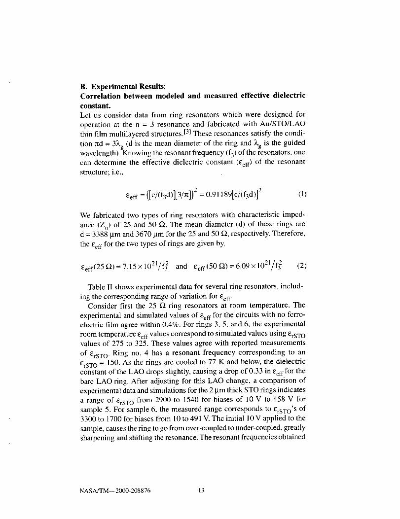
modeled data. Figure 16 shows a YBCO/STO (2 lam thick)/LAO
microstrip line at 77 K. Note that at 15 GHz and 400 V dc, the attenua-
tion is approximately 4 dB, which is also consistent with tan5 = 0.05.
0 J,L--3 ./ahlL
ip'1'_ -12
i-"+ /' I-2"I
10 12
FIGURE 13
I,-- 0 V Marker 1
13.725 GHz^_"_1- -5.8916 dB
/
'_v'_[J !50 V Marker 3-- 19.0 GHz
i -6.9285 dB
18 20
//
/,,, \III
14 16
Frequency (GHz)
Marker 2
16.5 GHz
-4.6807 dB
Experimental data for the attenuation versus frequency for a 1 cm
long, 50 _ Au/STO/LAO microstripline with a 2 I_m thick STO film at 77 K.
NASA/TM--2000-208876 16

4
A3-
_2-
0
0
FIGURE 14
I I I I I
1000 2000 3000 4000 5000 6000
Dielectric constant (_rSTO)
Modeled data at 15 GHz for the
attenuation of a Au/STO/LAO line with a 2 _m
STO film versus £rSTO for tan8 = 0.01.
E-6
.O"O
-9e'-
._om -12
-15
-18
0
-3 I ilL4 Marker 1
_ ,_ __ /; 100"13.725GHz_ -5.9026dB[ h;l_ "v '_ _ _ Marker 2
i " v,0 .z, -4.708 dB
t Marker 3
19.0 GHz
--6.9934 dB
-2110 2 14 16 18 20
Frequency (GHz)
FIGURE 15 Experimental data for the attenuation versus frequency for a I cmlong, 50 _ Au/STO/LAO microstripline with a 2 I_m thick STO film at 77 K (not
the same sample as in Fig. 13).
NASA/TM--2000-208876 17
A
E -5
eel
t-O
e-ID
<= -10
O 13.73 GHzA 15.0 GHz+ 19.0 GHz
I i i i I '
-15 i i i I i , i I , , I I , i I
-400 -200 0 200 400
Bias voltage (V)
FIGURE 16 Experimental data for the attenuation versus frequency for a
1 cm long, 50 _ YBCO/STO/LAO micrsotripline with a 2 IJm thick STO
film at 77 K.
These examples also show that the modeled data are helpful in assessing
the expected losses of a thin film ferroelectric-based tunable circuit.
C. Biasing Effects:
Before finishing this manuscript we would like to discuss briefly the
biasing effects on microstrip line-based ferroelectric circuits that are more
complicated than a single microstrip. When several adjacent microstrips
are employed, the dc biasing effects not only each line but also the
coupling between lines. One can bias different sections of the circuit dif-
ferently in order to optimize each section and/or the coupling between
sections. The effect of the applied dc electric field (primarily responsible
for tunability in these planar components) on the parameters such as the
insertion loss, center frequency, the return loss, and the bandwidth of the
microstrip resonators and bandpass filters have been studied experimen-
tally. [3] In the resonators, choosing the right biasing scheme, one can
optimize the coupling and sharpen the resonance while maintaining large
tunabilities.13] In the bandpass filters, one can reduce the insertion loss
of the pass-band, or maintain the passband relatively unchanged over a
tunable frequency range depending on the biasing scheme employed. U2]
Three different biasing schemes have been studied to date: (1) unipolar
NASA/TM--2000-208876 18
bias (UPB) where alternate nodes were biased positive, and ground,
(2) partial bipolar bias (PBB) where input and output lines were grounded,
and the resonator sections biased positive and negative alternatively,
(3) Full bipolar bias (FBB) where alternate sections (including the input
and output lines) were biased positive and negative. For a schematic rep-
resentation of the above biasing schemes we would like to refer the reader
to Fig. 1 of Ref. 12. It is important to note that the effective dielectric
constant of the microstrip structure depends upon the electric field
between the biased microstrip lines as well as the perpendicular field
between the top conductor and the ground plane. In general, the FBB
configuration gives the largest frequency tunability due to higher elec-
tric fields that can be applied in this configuration, and the PBB gave the
lowest insertion loss in the passband in the ferroelectric tunable microstrip
filters. Large tunability does not necessarily give the lowest insertion
loss for the filters. An important finding was that the percentage tunability
remained essentially the same for a specific applied electric field,
irrespective of the biasing scheme employed.[ 12l
V. CONCLUSIONS
A study on the correlation between the material properties and relevant
circuit parameters for ferroelectric thin film-based tunable microwave
components has been presented. The study considered structures based
on microstrip line configuration at frequencies from 10 to 20 GHz. Mod-
eled results of circuit parameters such as the characteristic impedance,
effective dielectric constant, and the attenuation in terms of ferroelectric
film's dielectric properties and thickness were presented. It was observed
that for a given substrate and ferroelectric thickness, smaller line width
results in higher tunability of the characteristic impedance and effective
dielectric constant. This implies that one can choose higher characteris-
tic impedance for obtaining larger frequency tunability as it is directly
related to the percentage change in Z o and eeff" The reliability of the
modeled data was tested against experimental data corresponding to two
specific types of components: ring resonators and microstrip transmis-
sion lines. In general, the modeled value for the effective dielectric
constant agreed reasonably well (i.e., within less than 6%) with those
measured experimentally. On the other hand, the deviation between mod-
eled and experimental data for the attenuation was of the order of 10%.
NASA/TM--2000-208876 19

This discrepancy may be attributed to other sources of losses present in
real circuits such as impedance mismatches originating from tempera-
ture or bias-induced variations of the ferroelectric's dielectric constant,
and conductor losses, which becomes more relevant at high frequencies. In
reality the problem is more complicated since it is known that there are
spatial variations of the dielectric constant of the ferroelectric film, either
intrinsic or bias induced, which were not taken into account in this study.
Nevertheless, the information presented here should facilitate selection
of appropriate electrical and geometrical parameters for practical appli-
cations of ferroelectric tunable microwaye components and circuits.
References
[1.] D.M. Dalbert, R.E. Stauber, J.C. Price, C.T. Rogers, and D. Gait,
Appl. Phys. Lett., 72, 507 (1998).
[2.] H-D. Wu and F.S. Barnes, Integrated Ferroelectrics 22, 291(1998).
[3.] F.W. Van Keuls, R.R. Romanofsky, D.Y. Bohman, and F.A.
Miranda, hTtegrated Ferroelectrics 22, 883 (1998).
[4.] G. Subramanyam, F.W. Van Keuls, and F.A. Miranda, IEEE
MTT-S Digest, 1011 (1998).
[5.] R.R. Romanofsky, F. W. Van Keuls, and F. A. Miranda, Journal de
Physique IV 8, 171 (1998).
[6.] EW. Van Keuls, R.R. Romanofsky, and EA. Miranda, Integrated
Ferroelectrics 22, 893 (1998).
[7.] J. Synowczynski, L.C. Sengupta, and L.H. Chu, Integrated Ferro-
electrics, 22, 861 (t998).
[8.] F.A. Miranda, C.H. Mueller, C.D. Cubbage, K.B. Bhasin, R.K.
Singh, and S.D. Harkness, IEEE Trans. on Appl. Supercond. 5,
3191 (1995).
Sonnet Software, Inc., Liverpool, NY, CA.; Zeland Software, Inc.,
Fremont, CA.
R.R. Romanofsky, "500 V X/K-Band Bias Tee" (unpublished).
M. Mejia, A.S. Creason, S.S. Toncich, B.T. Ebihara, and F.A.
Miranda, Advances in C_ogenic Engineering, 41, 1731 (1996).
G. Subramanyam, F.W. Van Keuls, F.A. Miranda, C.L. Canedy, S.
Aggarwal, T. Venkatesan, and R. Ramesh, Correlation of Electric
Field and Critical Design Parameters for Ferroelectric Tunable
Microwave Filters. Presented at the 11 th International Symposium
on Integrated Ferroelectrics, March 7-10, 1999, Colorado Springs,CO.
[9.]
[lO.][11.]
[12.]
NASA/TM--2000-208876 20


REPORT DOCUMENTATION PAGE I Form Approved
I OMB No. 0704-0188
Public reporting burden for this ¢ol)ection of information is estimated to average 1 hour per response, including the time for reviewing instructions, searching existing data sources,
gathering and maintaining the data needed, and completing and reviewing the collection of information. Send comments regarding this burden estimate or any other aspect of this
collection of information, including suggestions for reducing this burden, to Washington Headquarters Services, Directorate for Information Operations and Reports, 1215 Jefferson
Davis Highway, Suite 1204, Arlington, VA 22202-4302, and to the Office of Management and Budget, Paperwork Reduction Project (0704-0188), Washington, DC 20503,
1. AGENCY USE ONLY (Leave blank) 2. REPORT DATE 3. REPORT TYPE AND DATES COVERED
April 2000 Technical Memorandum
5. FUNDING NUMBERS4. TITLE AND SUBTITLE
Correlation Between Material Properties of Ferroelectric Thin Films and
Design Parameters for Microwave Device Applications: Modeling Examples
and Experimental Verification
6. AUTHOR(S)
F61ix A. Miranda, Fred W. Van Keuls, Guru Subramanyam, Carl H. Mueller,
Robert R. Romanofsky, and Gerardo Rosado
7. PERFORMING ORGANIZATION NAME(S) AND ADDRESS(ES)
National Aeronautics and Space Administration
John H. Glenn Research Center at Lewis Field
Cleveland, Ohio 44135- 3191
9. SPONSORING/MONITORING AGENCY NAME(S) AND ADDRESS(ES)
National Aeronautics and Space Administration
Washington, DC 20546-0001
WU- 632-6E-51--00
8. PERFORMING ORGANIZATIONREPORT NUMBER
E-11586
10. SPONSORING/MONITORINGAGENCY REPORT NUMBER
NASA TM--2000-208876
11. SUPPLEMENTARY NOTES
Prepared for the 1 lth International Symposium on Integrated Ferroelectrics cosponsored by the Gordon and Breach Science Publishers.
and the Univeristy of Colorado, Colorado Springs, Colorado, March 7-10, 1999. F61ix A. Miranda, Fred W. Van Keuls, Carl H. Mueller
and Robert R. Romanofsky, NASA Glenn Research Center; Guru Subramanyam, University of Dayton, 300 College Park, Dayton. Ohio
45469: Gerardo Rosado, University of Puerto Rico, Humacao, Puerto Rico 00791. Responsible person, F61ix A. Miranda, organization
code 5620, (216) 433-6589.
12a. DISTRIBUTION/AVAILABILITY STATEMENT
Unclassified - Unlimited
Subject Category: 33 Distribution: Nonstandard
This publication is available from the NASA Center for AeroSpace Information, (301) 621-0390.
12b. DISTRIBUTION CODE
13. ABSTRACT (Maximum 200 words)
The application of thin ferroelectric films for frequency and phase agile components is the topic of interest of many
research groups worldwide. Consequently, proof-of-concepts (POC) of different tunable microwave components using
either (HTS, metal)/ferroelectric thin film/dielectric heterostructures or (thick, thin) film "flip-chip" technology have been
reported. Either as ferroelectric thin film characterization tools or from the point of view of circuit implementation
approach, both configurations have their respective advantages and limitations. However, we believe that because of the
progress made so far using the heterostructure (i.e., multilayer) approach, and due to its intrinsic features such as planar
configuration and monolithic integration, a study on the correlation of circuit geometry aspects and ferroelectric material
properties could accelerate the insertion of this technology into working systems. In this paper, we will discuss our study
performed on circuits based on microstrip lines at frequencies above l0 GHz, where the multilayer configuration offers
greater ease of insertion due to circuit's size reduction. Modeled results of relevant circuit parameters such as the charac-
teristic impedance, effective dielectric constant, and attenuation as a function of ferroelectric film's dielectric constant,
tank, and thickness, will be presented for SrTiO 3 and BaxSrl_xTiO3 ferroelectric films. A comparison between the
modeled and experimental data for some of these parameters will be presented.
14. SUBJECT TERMS
Ferroelectric films: Tunable microwave components; Microstripline configuration: Characteristic
impedance: Effective dielectric constant: Attenuation: SrTiO3:BaxSrl_xTiO3; LaAIO3:10-20 GHz
17. SECURITY CLASSIFICATIONOF REPORT
Unclassified
18. SECURITY CLASSIFICATIONOF THIS PAGE
Unclassified
19. SECURITY CLASSIFICATIONOF ABSTRACT
Unclassified
15. NUMBER OF PAGES26
16. PRICE CODE
A0320. LIMITATION OF ABSTRACT
NSN 7540-01-280-5500 Standard Form 298 (Rev. 2-89)Prescribedby ANSI Std. Z39-18298-102

![689 ' # '5& *#6 & 7 · Ferroelectrics Material Aspects 364 properties of ferroelectric thin films [13-16]. Change of film strain field, either tensile or compressive, will elongate](https://img.dokumen.tips/doc/110x75/5fa8f203bb4f2c76533550ca/689-5-6-7-ferroelectrics-material-aspects-364-properties-of-ferroelectric.jpg)