Embed Size (px)
Citation preview
7/28/2019 corg
http://slidepdf.com/reader/full/corg 1/62
BITS Pilani, Pilani Campus
Components of a Computer
Input (mouse, keyboard, …)
Output (display, printer, …)
Memory
–main (DRAM), cache (SRAM)
– secondary (disk,
CD, DVD, …)
Datapath
Control
Input
Processor
Control
Datapath
Output
Memory10010100101100000010100101010001
1111011101100110
1001010010110000
1001010010110000
1001010010110000
Processor
(CPU)

7/28/2019 corg
http://slidepdf.com/reader/full/corg 2/62
BITS Pilani, Pilani Campus
Von Neumann architecture
Single bank of memory which processor accesses through
a single set of address and data lines.
Processor core
Address bus
Memory
Data bus
7/28/2019 corg
http://slidepdf.com/reader/full/corg 3/62
BITS Pilani, Pilani Campus
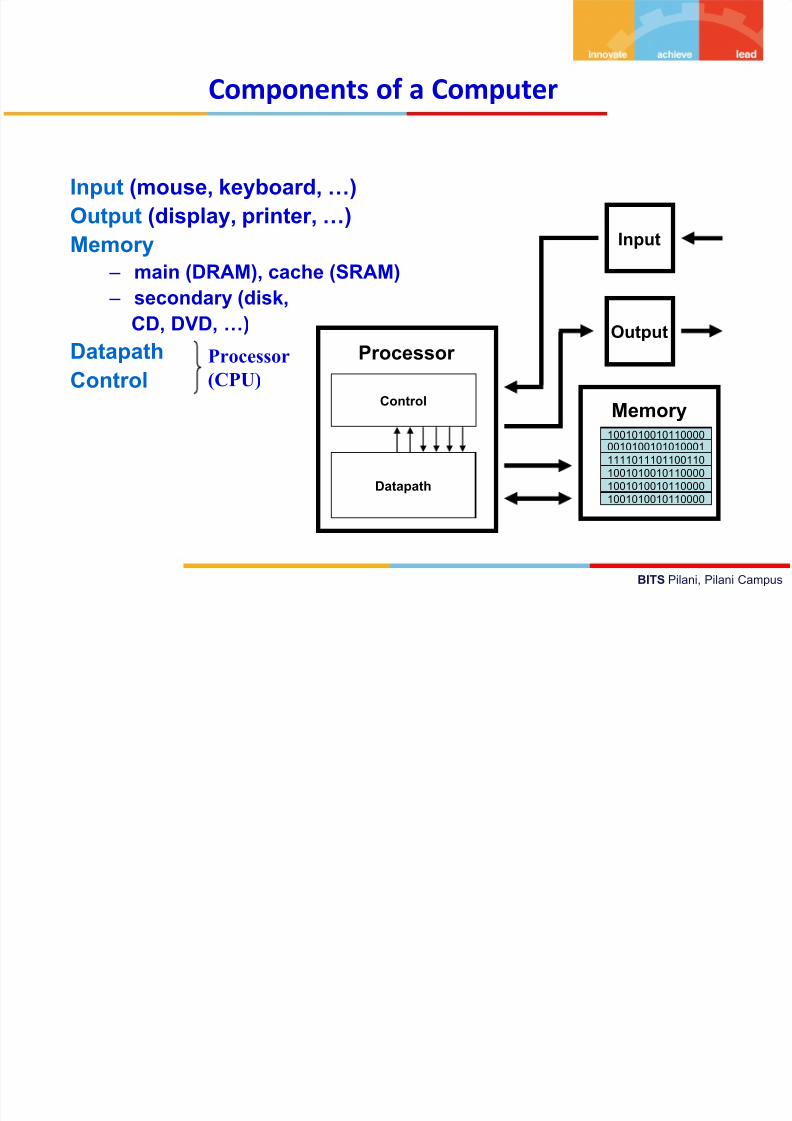
Harvard Architecture
Processor connected to two independent memory banks
via two independent set of buses.
Program bank and Data bank
Program bank will hold program instructions and data
bank with data.

7/28/2019 corg
http://slidepdf.com/reader/full/corg 4/62
BITS Pilani, Pilani Campus
A CISC Architecture
Larger instructions with variable formats
(16-64 bits/ instruction)
Larger Addressing Modes (12- 24)
Few Registers
Most Microcoded with control Memory
Close to high level language
7/28/2019 corg
http://slidepdf.com/reader/full/corg 5/62
BITS Pilani, Pilani Campus
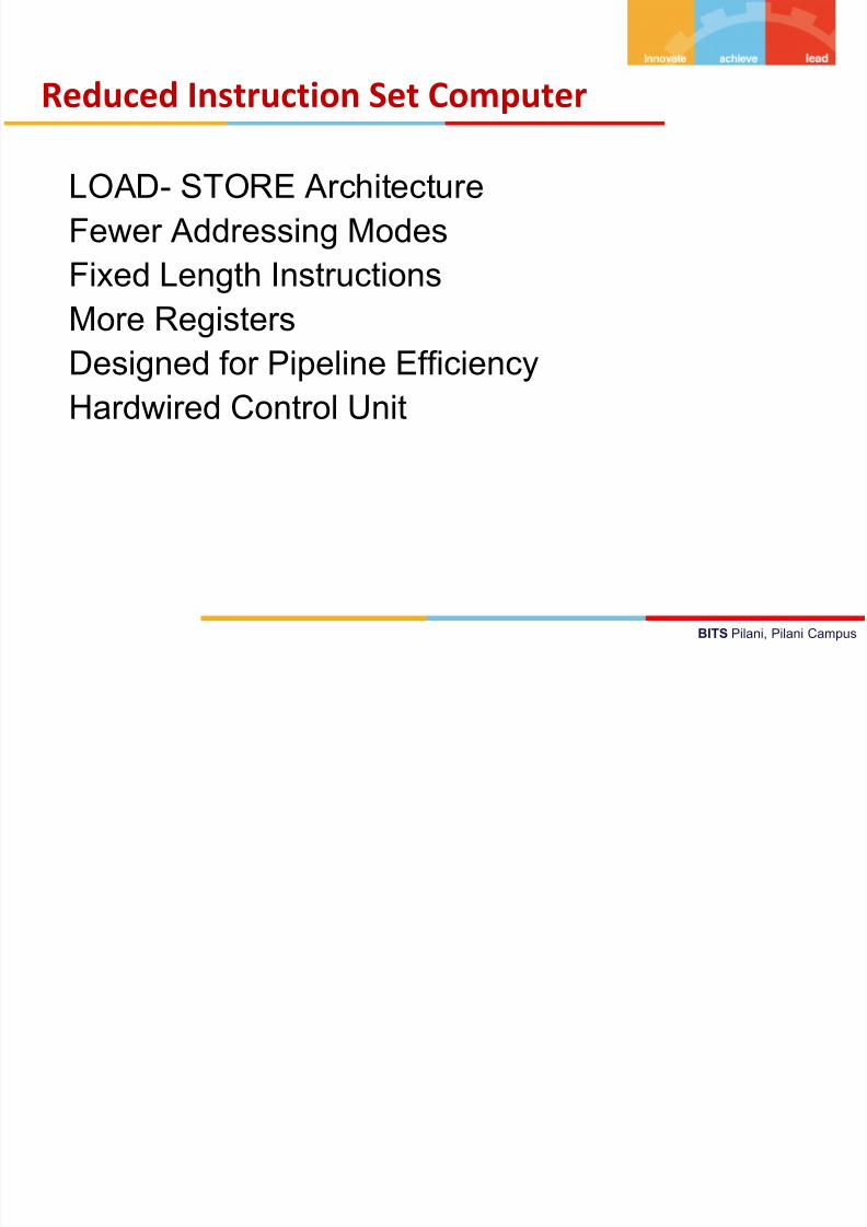
Reduced Instruction Set Computer
LOAD- STORE Architecture
Fewer Addressing Modes
Fixed Length Instructions
More Registers
Designed for Pipeline Efficiency
Hardwired Control Unit
7/28/2019 corg
http://slidepdf.com/reader/full/corg 6/62
BITS Pilani, Pilani Campus
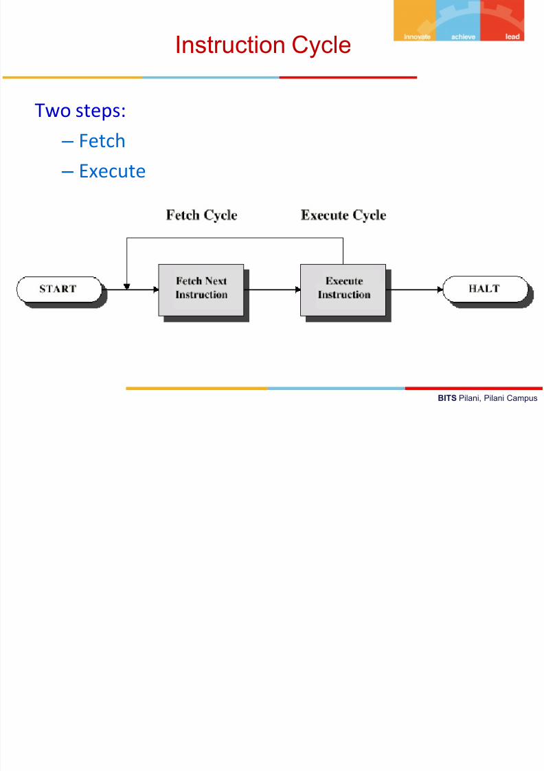
Instruction Cycle
Two steps:
– Fetch
– Execute
7/28/2019 corg
http://slidepdf.com/reader/full/corg 7/62BITS Pilani, Pilani Campus
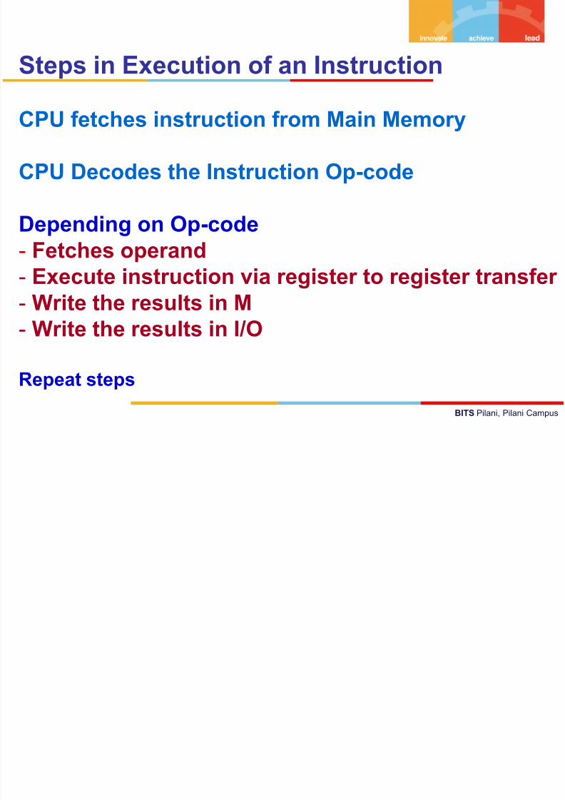
Steps in Execution of an Instruction
CPU fetches instruction from Main Memory
CPU Decodes the Instruction Op-code
Depending on Op-code
- Fetches operand
- Execute instruction via register to register transfer
- Write the results in M- Write the results in I/O
Repeat steps
7/28/2019 corg
http://slidepdf.com/reader/full/corg 8/62BITS Pilani, Pilani Campus
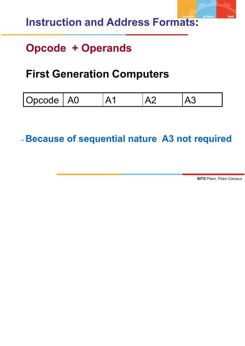
Instruction and Address Formats:
Opcode + Operands
First Generation Computers
Opcode A0 A1 A2 A3
- Because of sequential nature A3 not required
7/28/2019 corg
http://slidepdf.com/reader/full/corg 9/62BITS Pilani, Pilani Campus
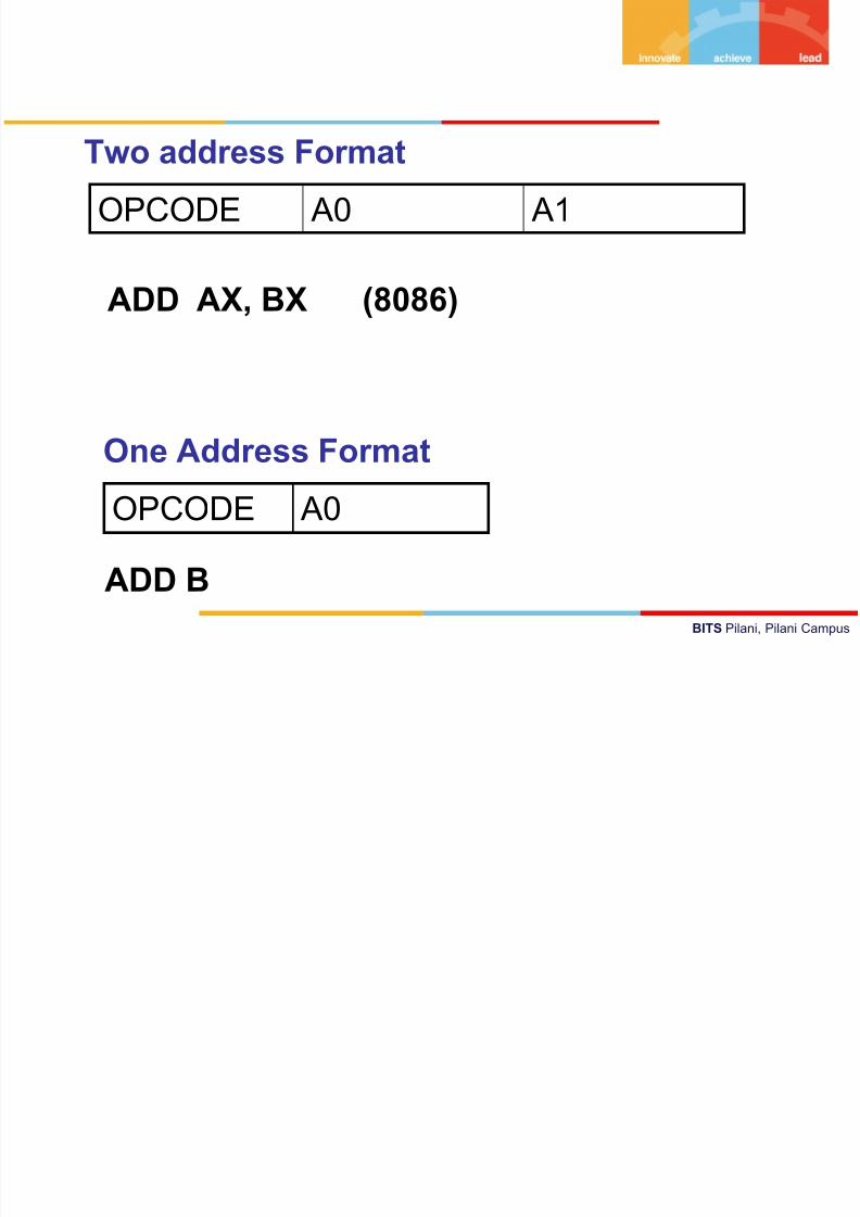
Two address Format
OPCODE A0 A1
ADD AX, BX (8086)
One Address Format
OPCODE A0
ADD B

7/28/2019 corg
http://slidepdf.com/reader/full/corg 10/62BITS Pilani, Pilani Campus
Zero address Machines:
(Stack Machines)
ADD
Ex:
X = A*B + C*D

7/28/2019 corg
http://slidepdf.com/reader/full/corg 11/62BITS Pilani, Pilani Campus
REG SET
ALU
CLU
CENTRAL PROCESSING UNIT

7/28/2019 corg
http://slidepdf.com/reader/full/corg 12/62BITS Pilani, Pilani Campus
Clock Generator Bus Controller
Processor Controller
Execution Unit
A SINGLE CHIP MICROPROCESSOR
Control Part
Data Part

7/28/2019 corg
http://slidepdf.com/reader/full/corg 13/62BITS Pilani, Pilani Campus
EXECUTION UNIT
Programmers Register set
Additional registers ( IR, PC , Temp Reg)
ALU and any special function units
Internal Data paths
All connected through a interconnect network
usually comprised of one/more buses
7/28/2019 corg
http://slidepdf.com/reader/full/corg 14/62BITS Pilani, Pilani Campus
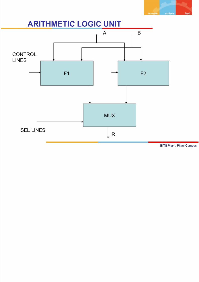
ARITHMETIC LOGIC UNIT
F1 F2
MUX
A B
SEL LINES
CONTROL
LINES
R
7/28/2019 corg
http://slidepdf.com/reader/full/corg 15/62BITS Pilani, Pilani Campus
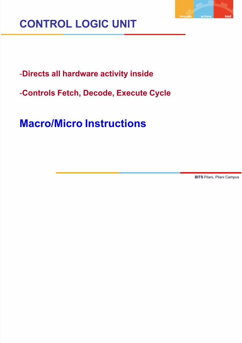
CONTROL LOGIC UNIT
-Directs all hardware activity inside
-Controls Fetch, Decode, Execute Cycle
Macro/Micro Instructions
7/28/2019 corg
http://slidepdf.com/reader/full/corg 16/62BITS Pilani, Pilani Campus
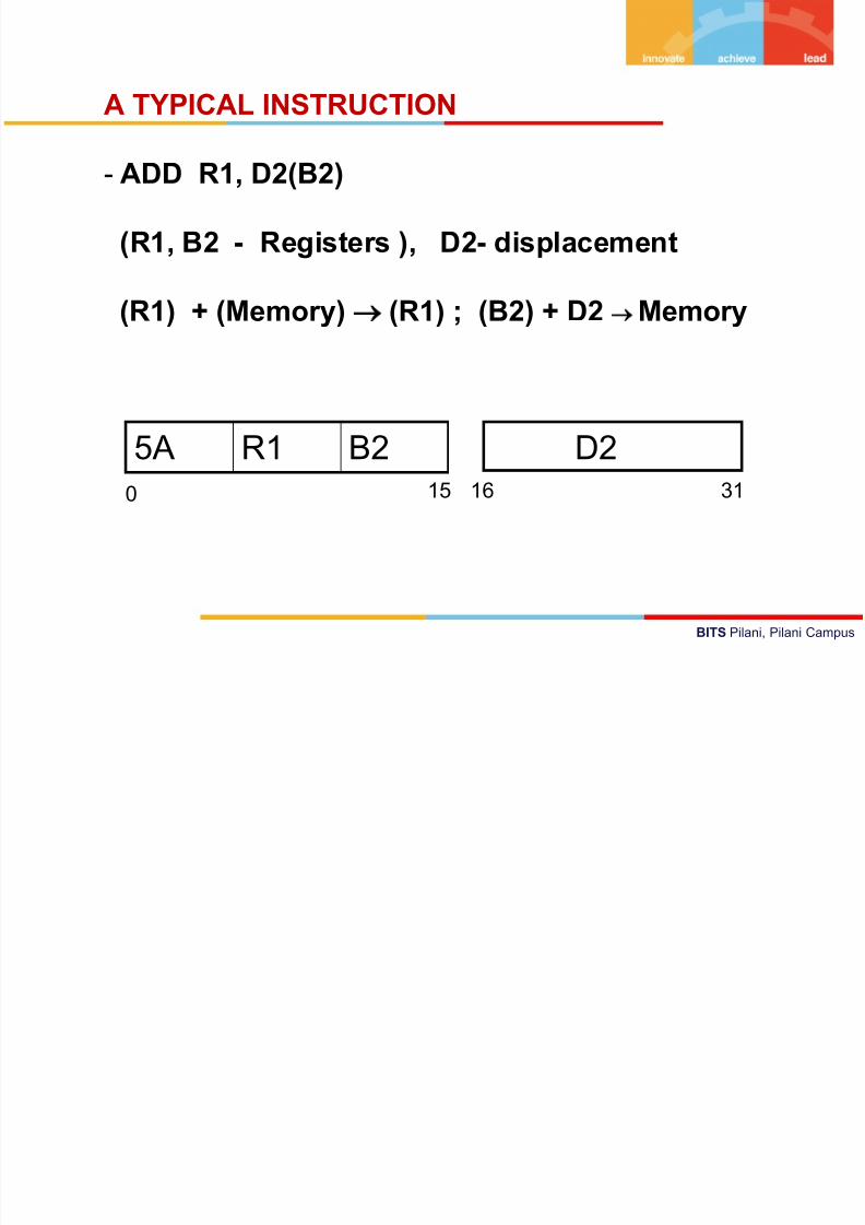
A TYPICAL INSTRUCTION
- ADD R1, D2(B2)
(R1, B2 - Registers ), D2- displacement
(R1) + (Memory) (R1) ; (B2) + D2 Memory
5A R1 B2 D20 15 16 31

7/28/2019 corg
http://slidepdf.com/reader/full/corg 17/62BITS Pilani, Pilani Campus
CPU Operations
Fetch a word from Memory
Store a word into memory
Reg Transfers
Performing an ALU function

7/28/2019 corg
http://slidepdf.com/reader/full/corg 18/62BITS Pilani, Pilani Campus
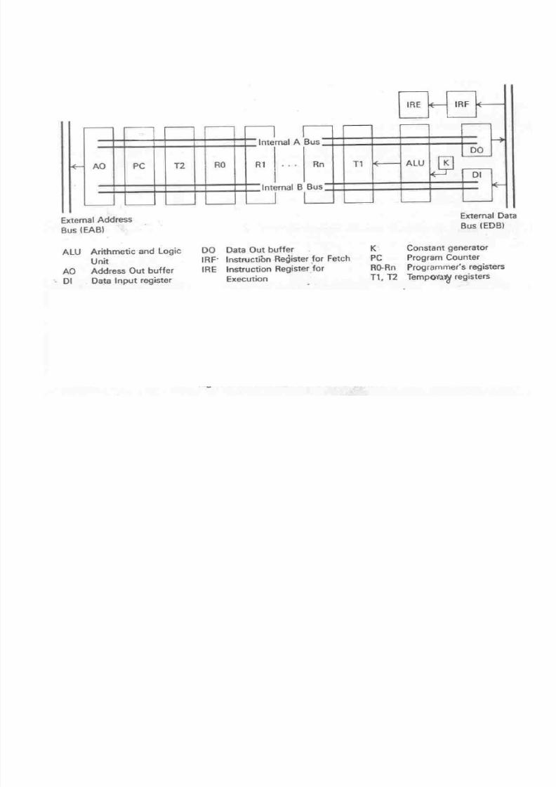
Instruction Decoder
IR
PC
MAR
MDR
R0
Rn-1
Y
ALU
Z
Address Bus
Data Bus
C P U B
u s
A BControl Lines
Clear Y
7/28/2019 corg
http://slidepdf.com/reader/full/corg 19/62BITS Pilani, Pilani Campus
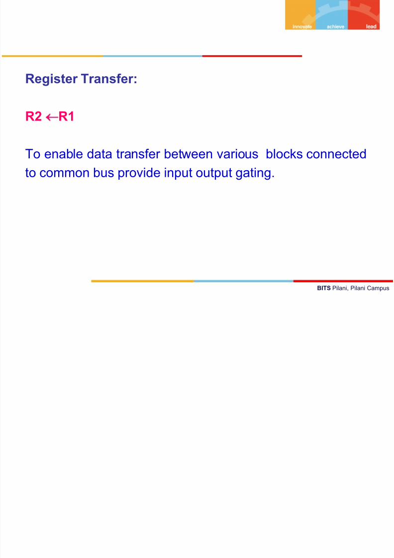
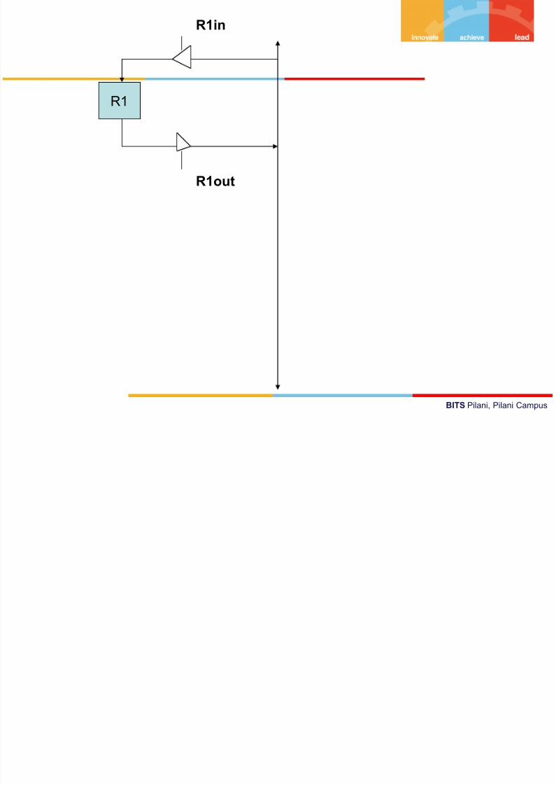
Register Transfer:
R2R1
To enable data transfer between various blocks connected
to common bus provide input output gating.
7/28/2019 corg
http://slidepdf.com/reader/full/corg 20/62BITS Pilani, Pilani Campus
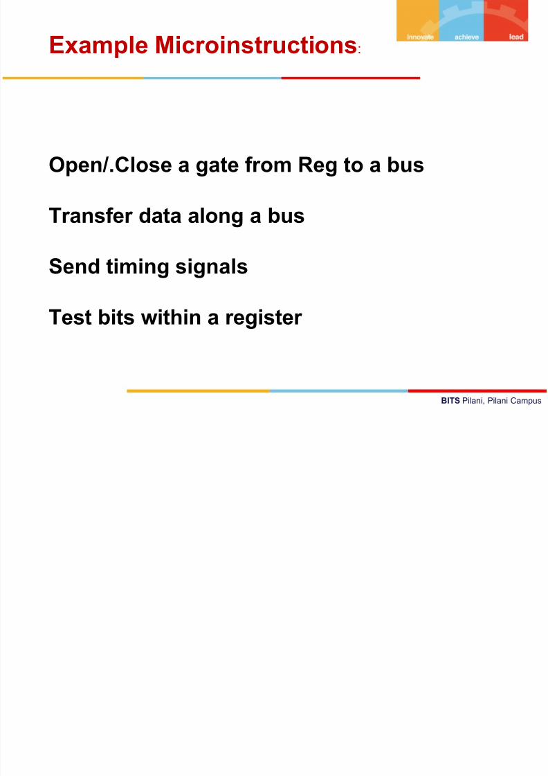
Example Microinstructions:
Open/.Close a gate from Reg to a bus
Transfer data along a bus
Send timing signals
Test bits within a register
7/28/2019 corg
http://slidepdf.com/reader/full/corg 21/62BITS Pilani, Pilani Campus
R1
R1in
R1out
7/28/2019 corg
http://slidepdf.com/reader/full/corg 22/62BITS Pilani, Pilani Campus
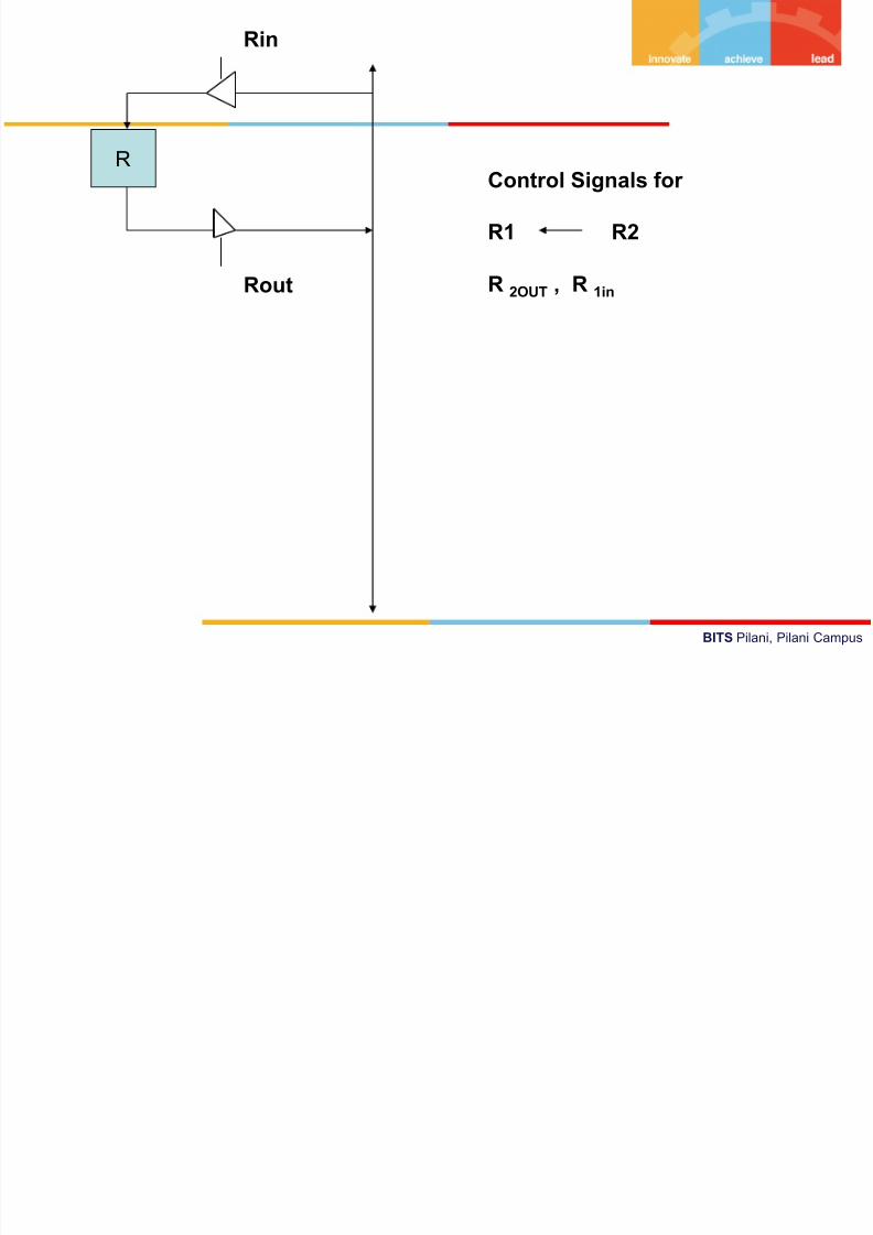
R
Rin
Rout
Control Signals for
R1 R2
R 2OUT , R 1in

7/28/2019 corg
http://slidepdf.com/reader/full/corg 23/62
BITS Pilani, Pilani Campus
Fetching a word from memory:
i. MAR (R1)
ii. Read Signal
iii. Wait for Memory-function-complete
(MFC) signaliv. R2(MDR)

7/28/2019 corg
http://slidepdf.com/reader/full/corg 24/62
BITS Pilani, Pilani Campus
Storing a word into Memory:
i. MAR (R1)
ii. MDR (R2)
iii. Memory write signal
iv. Wait for MFC
7/28/2019 corg
http://slidepdf.com/reader/full/corg 25/62
BITS Pilani, Pilani Campus
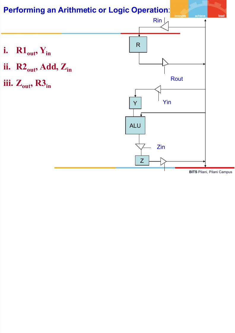
Performing an Arithmetic or Logic Operation:
i. R1out, Yin
ii. R2out, Add, Zin
iii. Zout, R3in
R
Rin
Rout
ALU
Y
Z
Zin
Yin

7/28/2019 corg
http://slidepdf.com/reader/full/corg 26/62
BITS Pilani, Pilani Campus
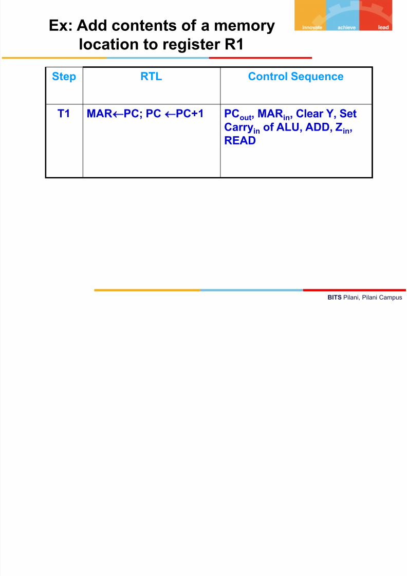
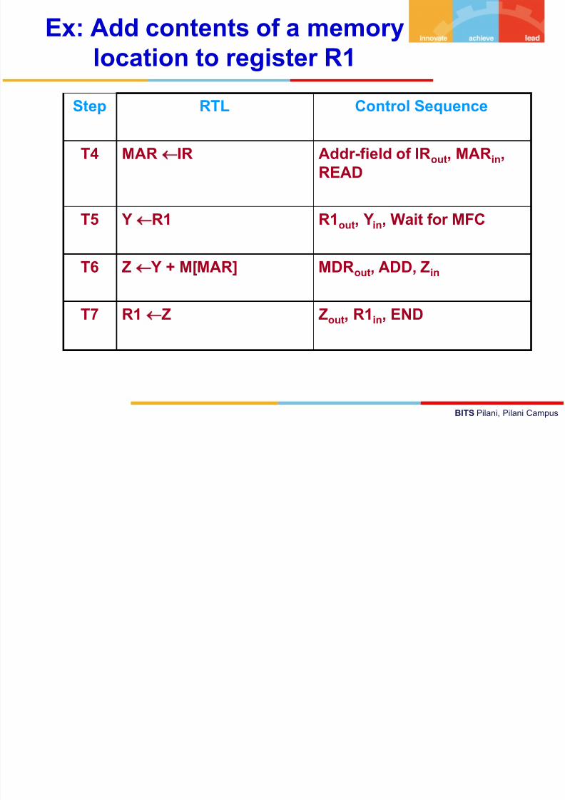
Ex: Add contents of a memory
location to register R1
(Address of Memory location is in part of
the instruction )
7/28/2019 corg
http://slidepdf.com/reader/full/corg 27/62
BITS Pilani, Pilani Campus
Step RTL Control Sequence
T1 MARPC; PCPC+1 PCout, MARin, Clear Y, Set
Carryin of ALU, ADD, Zin,
READ
Ex: Add contents of a memory
location to register R1
7/28/2019 corg
http://slidepdf.com/reader/full/corg 28/62
BITS Pilani, Pilani Campus
Step RTL Control Sequence
T1 MARPC; PCPC+1 PCout, MARin, Clear Y, Set
Carryin of ALU, ADD, Zin,
READ
T2 Wait Zout, PCin, Wait for MFC
T3 IRMDR MDRout, IRin
Ex: Add contents of a memory
location to register R1
- Instruction Fetch
7/28/2019 corg
http://slidepdf.com/reader/full/corg 29/62
BITS Pilani, Pilani Campus
Step RTL Control Sequence
T4 MARIR Addr-field of IRout, MARin,
READ
T5 YR1 R1out, Yin, Wait for MFC
T6 Z Y + M[MAR] MDRout, ADD, Zin
T7 R1Z Zout, R1in, END
Ex: Add contents of a memory
location to register R1
7/28/2019 corg
http://slidepdf.com/reader/full/corg 30/62
BITS Pilani, Pilani Campus
Step RTL Control Sequence
T1 MARPC; PCPC+1 PCout, MARin, Clear Y, Set
Carryin of ALU, ADD, Zin,
READ
T2 Wait Zout, PCin, Wait for MFC
T3 IRMDR MDRout, IRin
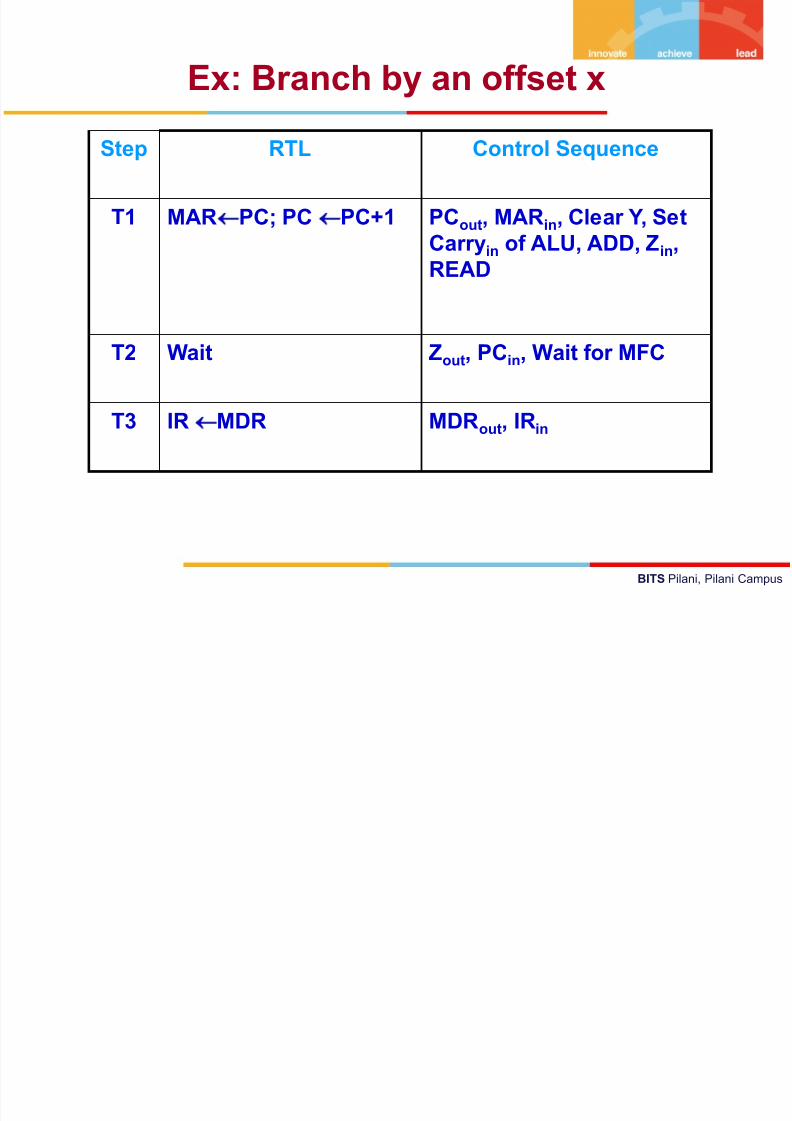
Ex: Branch by an offset x

7/28/2019 corg
http://slidepdf.com/reader/full/corg 31/62
Step RTL Control Sequence
T4 YPC PCout, Yin
T5 Z Y + [x of IR] ADD, Zin Addr-field of IRout
T6 PC
Z Zout, PCin, END
Ex: Branch by an offset x

7/28/2019 corg
http://slidepdf.com/reader/full/corg 32/62
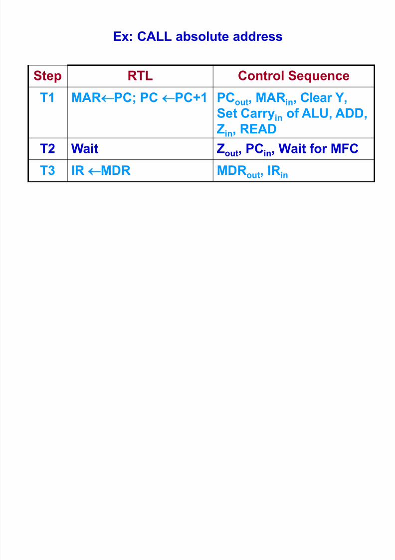
Ex: CALL absolute address
-Address fetched along with
instruction
7/28/2019 corg
http://slidepdf.com/reader/full/corg 33/62
Step RTL Control Sequence
T1 MARPC; PCPC+1 PCout, MARin, Clear Y,
Set Carryin of ALU, ADD,
Zin, READ
T2 Wait Zout, PCin, Wait for MFC
T3 IRMDR MDRout, IRin
Ex: CALL absolute address
7/28/2019 corg
http://slidepdf.com/reader/full/corg 34/62
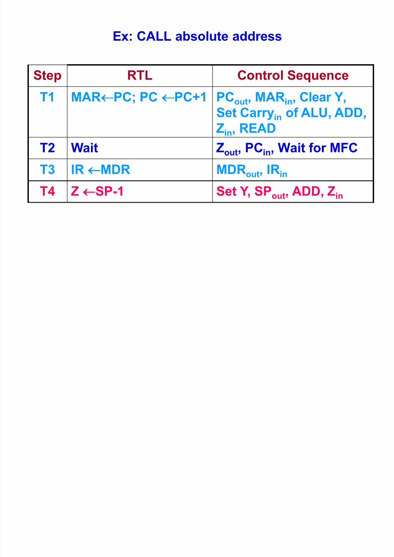
Step RTL Control Sequence
T1 MARPC; PCPC+1 PCout, MARin, Clear Y,
Set Carryin of ALU, ADD,
Zin, READ
T2 Wait Zout, PCin, Wait for MFC
T3 IRMDR MDRout, IRin
T4 ZSP-1 Set Y, SPout, ADD, Zin
Ex: CALL absolute address
7/28/2019 corg
http://slidepdf.com/reader/full/corg 35/62
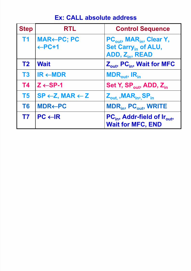
Step RTL Control Sequence
T1 MARPC; PC
PC+1
PCout, MARin, Clear Y,
Set Carryin of ALU,
ADD, Zin, READ
T2 Wait Zout
, PCin
, Wait for MFC
T3 IRMDR MDRout, IRin
T4 ZSP-1 Set Y, SPout, ADD, Zin
T5 SPZ, MAR Z Zout, ,MARin,,SPin
T6 MDRPC MDRin, PCout, WRITE
T7 PCIR PCin, Addr-field of Ir out,
Wait for MFC, END
Ex: CALL absolute address

7/28/2019 corg
http://slidepdf.com/reader/full/corg 36/62
Load Register from Memory
with Absolute address
( LDA 1000)

7/28/2019 corg
http://slidepdf.com/reader/full/corg 37/62
Step RTL Control Sequence
T1 MARPC; PCPC+1 PCout, MARin, Clear Y, Set
Carryin of ALU, ADD, Zin,
READ
T2 Wait Zout, PCin, Wait for MFC
T3 IRMDR MDRout, IRin
T4 MAR IR Add field of IRout, READ
T5 Wait Wait for MFC
T6 R2 MDR MDRout, R2in
7/28/2019 corg
http://slidepdf.com/reader/full/corg 38/62
7/28/2019 corg
http://slidepdf.com/reader/full/corg 39/62
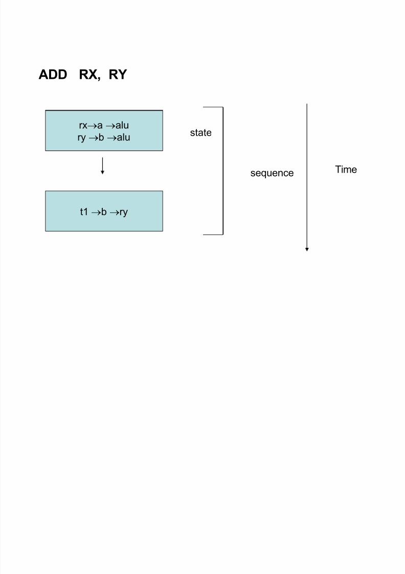
ADD RX, RY
rxaalu
rybalu
t1
b
ry
state
sequence Time

7/28/2019 corg
http://slidepdf.com/reader/full/corg 40/62
Design of CLU
- Hard wired design
- Microprogrammed design

7/28/2019 corg
http://slidepdf.com/reader/full/corg 41/62
HARDWIRED CONTROL UNIT

7/28/2019 corg
http://slidepdf.com/reader/full/corg 42/62
Hard-wired Control Unit
The opcode field of IR. This field is decoded toprovide the encoder information about
instruction being decoded
-Signals from status and condition
-Control step information
( Step generator for T1, T2, ….)
-External signals such as start, MFC,
interrupts etc.
7/28/2019 corg
http://slidepdf.com/reader/full/corg 43/62
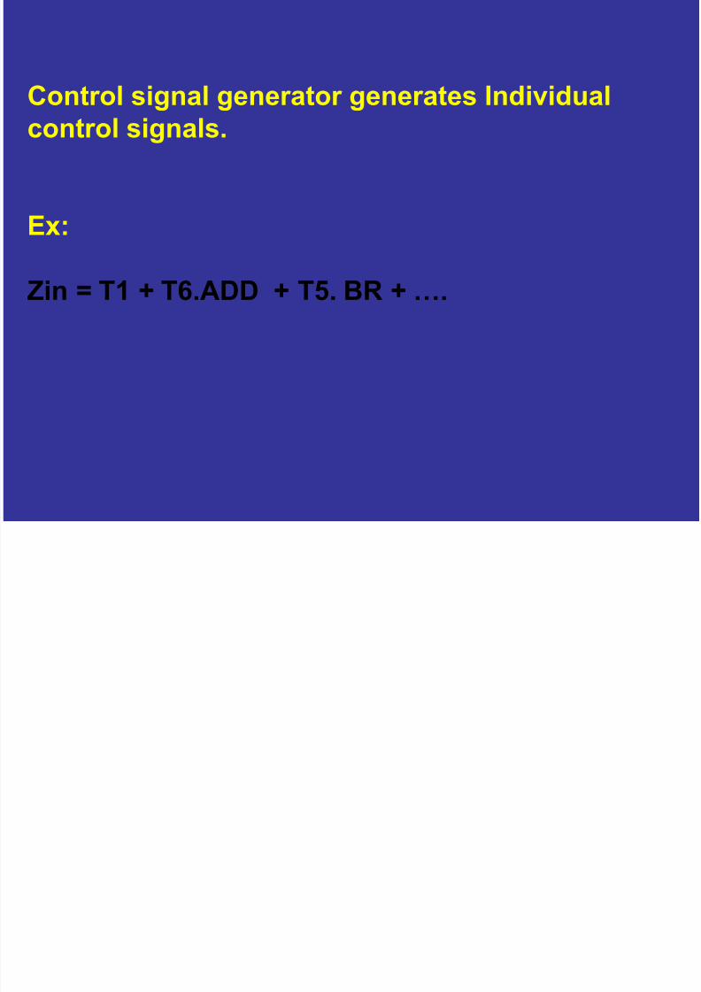
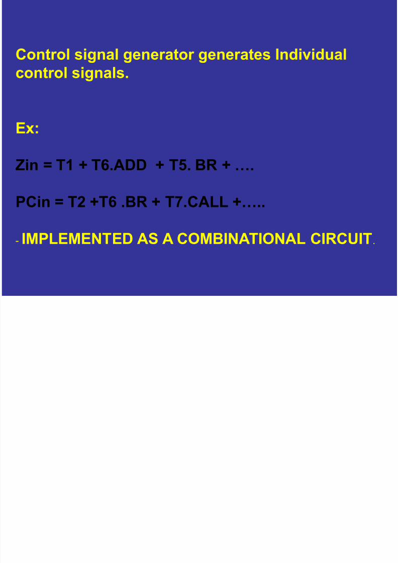
Control signal generator generates Individual
control signals.
Ex:
Zin = T1 + T6.ADD + T5. BR + ….
7/28/2019 corg
http://slidepdf.com/reader/full/corg 44/62
Control signal generator generates Individual
control signals.
Ex:
Zin = T1 + T6.ADD + T5. BR + ….
PCin = T2 +T6 .BR + T7.CALL +…..
- IMPLEMENTED AS A COMBINATIONAL CIRCUIT.
7/28/2019 corg
http://slidepdf.com/reader/full/corg 45/62
Combinational design could be using PLDs.
Hard wired logic difficult to implement changes
Provides faster execution.
Another approach
Microprogrammed control unit

7/28/2019 corg
http://slidepdf.com/reader/full/corg 46/62
Microprogrammed Unit
-Sequence of microinstructions corresponding
to each instruction is stored in ROM called
Control Memory
-Called Microprogram
-Provides flexibility of implementation
-Less hardware
7/28/2019 corg
http://slidepdf.com/reader/full/corg 47/62
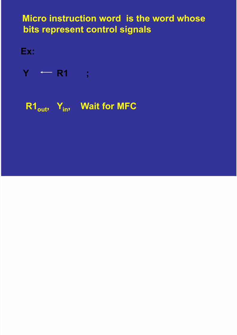
Micro instruction word is the word whose
bits represent control signals
Ex:
Y R1 ;
R1out, Yin, Wait for MFC
7/28/2019 corg
http://slidepdf.com/reader/full/corg 48/62
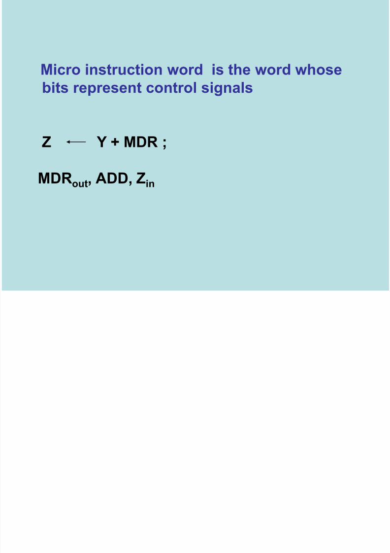
Micro instruction word is the word whosebits represent control signals
Z Y + MDR ;
MDRout, ADD, Zin
7/28/2019 corg
http://slidepdf.com/reader/full/corg 49/62
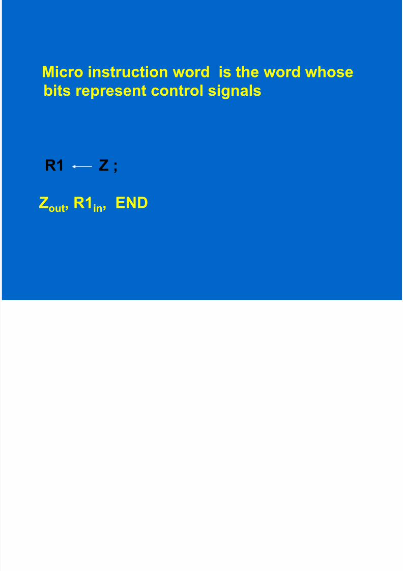
Micro instruction word is the word whosebits represent control signals
R1 Z ;
Zout, R1in, END

7/28/2019 corg
http://slidepdf.com/reader/full/corg 50/62
Step :R1in R1out Yin Zin Zout MDRout ADD WMFC END
5 0 1 1 0 0 0 0 1 0
6 0 0 0 1 0 1 1 0 0
7 1 0 0 0 1 0 0 0 1

7/28/2019 corg
http://slidepdf.com/reader/full/corg 51/62
Microprogramming Types
Horizontal Microprogramming
Vertical Microprogramming

7/28/2019 corg
http://slidepdf.com/reader/full/corg 52/62
Horizontal Approach
-1 bit per control signal
-Many control signals generated concurrently
-Permitting very fast operation
-Requires large control memory area
7/28/2019 corg
http://slidepdf.com/reader/full/corg 53/62
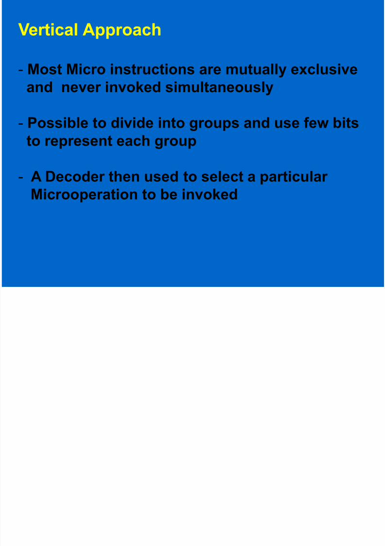
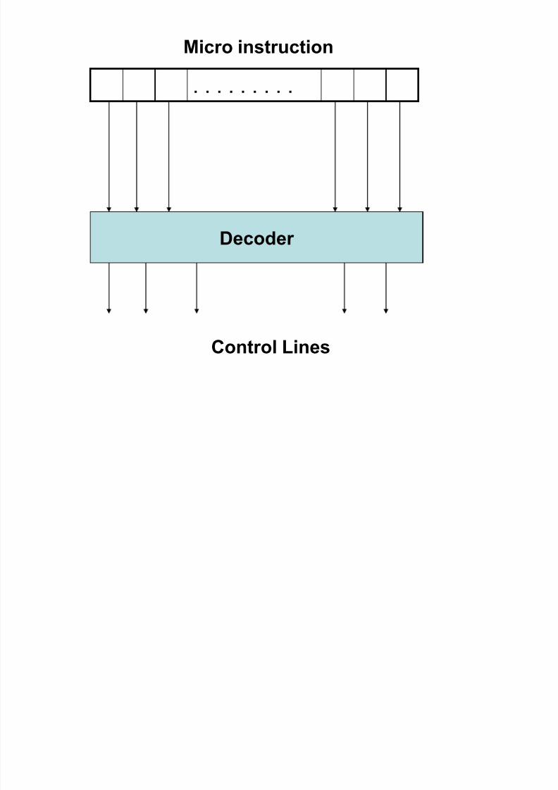
Vertical Approach
- Most Micro instructions are mutually exclusiveand never invoked simultaneously
- Possible to divide into groups and use few bits
to represent each group
- A Decoder then used to select a particular
Microoperation to be invoked
7/28/2019 corg
http://slidepdf.com/reader/full/corg 54/62
. . . . . . . . .
Decoder
Micro instruction
Control Lines

7/28/2019 corg
http://slidepdf.com/reader/full/corg 55/62
-Resembles Macro instruction
-Easier to write
-Control Memory size reduced
-Additional hardware required
-Slow down the process
Combinational approach can be used
7/28/2019 corg
http://slidepdf.com/reader/full/corg 56/62
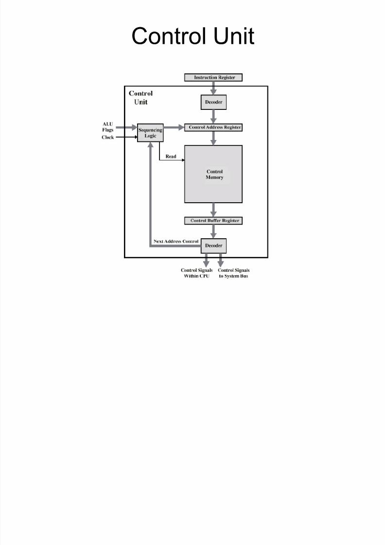
Control Unit
7/28/2019 corg
http://slidepdf.com/reader/full/corg 57/62
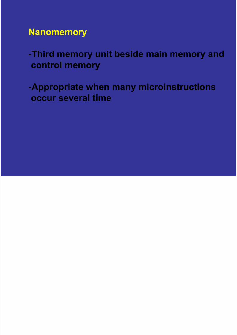
Nanomemory
-Third memory unit beside main memory and
control memory
-Appropriate when many microinstructionsoccur several time

7/28/2019 corg
http://slidepdf.com/reader/full/corg 58/62
Example:
Microprogram with k t-bit micro instructions
To store this k x t size control memory required
Assume only n distinct microinstructions are
used where n k
Store these instr ctions in n ord t bit nanomemor

7/28/2019 corg
http://slidepdf.com/reader/full/corg 59/62
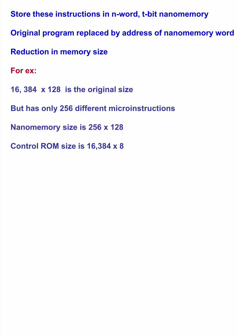
Store these instructions in n-word, t-bit nanomemory
Original program replaced by address of nanomemory word
Reduction in memory size
Store these instructions in n word t bit nanomemory
7/28/2019 corg
http://slidepdf.com/reader/full/corg 60/62
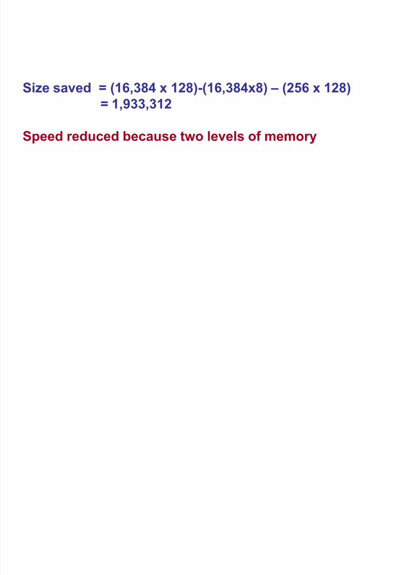
Store these instructions in n-word, t-bit nanomemory
Original program replaced by address of nanomemory word
Reduction in memory size
For ex:
16, 384 x 128 is the original size
But has only 256 different microinstructions
Nanomemory size is 256 x 128
Control ROM size is 16,384 x 8
7/28/2019 corg
http://slidepdf.com/reader/full/corg 61/62
Size saved = (16,384 x 128)-(16,384x8) – (256 x 128)
= 1,933,312
Speed reduced because two levels of memory
7/28/2019 corg
http://slidepdf.com/reader/full/corg 62/62
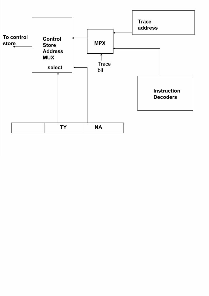
MPXControlStore
Address
MUX
select
TY NA
Instruction
Decoders
Trace
address
Trace
bit
To controlstore