Embed Size (px)
Citation preview

Core3DES v3.1 Handbook

Core3DES v3.1 Handbook
Table of Contents
Introduction .................................................................................................................... 3 Core Overview ............................................................................................................................................... 3 Design Security.............................................................................................................................................. 5 Key Features ................................................................................................................................................. 5 Core Version .................................................................................................................................................. 5 Supported Families ........................................................................................................................................ 6 Device Utilization and Performance ............................................................................................................ 6
Design Description ........................................................................................................ 7 I/O Signals ..................................................................................................................................................... 7 Parameters/Generics ..................................................................................................................................... 8
Functional Block Description ....................................................................................... 9
Core3DES Operation ................................................................................................... 10 Selecting a Cipher Key ................................................................................................................................ 10 Parity Checking............................................................................................................................................ 10 Encryption .................................................................................................................................................... 11 Decryption .................................................................................................................................................... 12 Pause/Resume ............................................................................................................................................ 13 Clear/Abort ................................................................................................................................................... 14 Modes of Operation ..................................................................................................................................... 14
Tool Flows and Testbench Operation ........................................................................ 15 License ........................................................................................................................................................ 15 SmartDesign ................................................................................................................................................ 15 Simulation Flows.......................................................................................................................................... 15 Synthesis in Libero ...................................................................................................................................... 16 Place-and-Route in Libero ........................................................................................................................... 16
Testbench Operation ................................................................................................... 17
Ordering Information ................................................................................................... 18 Ordering Codes ........................................................................................................................................... 18 Export Restrictions....................................................................................................................................... 18
List of Changes ............................................................................................................ 19
Product Support ........................................................................................................... 20 Customer Service ........................................................................................................................................ 20 Customer Technical Support Center ........................................................................................................... 20 Technical Support ........................................................................................................................................ 20 Website ........................................................................................................................................................ 20 Contacting the Customer Technical Support Center ................................................................................... 20 ITAR Technical Support .............................................................................................................................. 21
Core3DES v3.1 Handbook 2

Introduction
Core Overview The Core3DES macro implements the Triple Data Encryption Standard (3DES or Triple DES), which provides a means of securing data. The Triple DES algorithm is described in the Federal Information Processing Standards (FIPS) Publication (PUB) 46-3, and is an extension of the DES (Data Encryption Standard) algorithm (Figure 1) and also described in FIPS PUB 46-3. The Triple DES algorithm takes as inputs 64 bits of plaintext data and 192 bits of a cipher key, and after 48 cycles, produces a 64-bit ciphered version of the original plaintext data as output.1 The entire 168-bit cipher key consists of three sub-keys, denoted as K1, K2, and K3, representing the left third (MSB), the middle third, and the right third (LSB) of the cipher key, respectively. During the 48 cycles, or iterations, of the algorithm, the data bits are subjected to permutation and addition functions, which consist of key schedules, calculated by rotations and permutations applied to the original 168-bit cipher key.
Input
Initial Permutation
Inverse Initial Permutation
Output
16 Rounds of Computation
Key
L0
L1=R0
L2=R1
R16=L15f(R15,K16)
R0
R1=L0f(R0,K1)
R2=L1f(R1,K2)
L16=R15
+
+f
f
.
.
....
Left and RightData Halves after Initial Permutation
Key Schedule 1K1
K2
Left and RightData Halves after Round 2
Left and RightData Halves after Round 16
Left and Right
Key Schedule 2Round 1
Figure 1 DES Algorithm
1 Only 168 of the 192 bits of the key are used in the calculations, as the least significant bit of each byte of the cipher key is used to provide oddparity for the key bytes.
Core3DES v3.1 Handbook 3

Introduction
The Triple DES encryption algorithm is executed in the specific sequential order shown in Figure 2. 1. Encrypt using DES with cipher key K1 (left third of 168-bit cipher key). 2. Decrypt using DES with cipher key K2 (middle third of 168-bit cipher key). 3. Encrypt using DES with cipher key K3 (right third of 168-bit cipher key).
K1
DES (Encrypt)
K2
DES (Decrypt)
K3
DES (Encrypt) Ciphertext DataPlaintext Data
Figure 2 Encryption Flow Diagram for 3DES
The Triple DES decryption algorithm is executed in the specific sequential order shown in Figure 3. 1. Decrypt using DES with cipher key K3 (right third of 168-bit cipher key). 2. Encrypt using DES with cipher key K2 (middle third of 168-bit cipher key). 3. Decrypt using DES with cipher key K1 (left third of 168-bit cipher key).
K3
DES (Decrypt)
K2
DES (Encrypt)
K1
DES (Decrypt) Ciphertext Data Plaintext Data
Figure 3 Decryption Flow Diagram for 3DES
Since three sequential DES operations are required, the total compute time for Triple DES (encryption or decryption) is three times that for single DES, or 16 x 3 = 48 clock cycles.
4 Core3DES v3.1 Handbook

Design Security
Design Security Figure 4 shows a typical system diagram. Note that the cipher key, which is the "secret" key, can be made up of FPGA logic cells, thereby preventing the possibility of design or data theft. Microsemi® Flash-based devices (ProASIC3) employ FlashLock™ technology, and Microsemi antifuse-based devices (Axcelerator, SX-A, RT54SX-S) employ FuseLock™ technology, each of which provides a means to keep the cipher key and the rest of the logic secure. The output of the Core3DES macro should be connected to registers or FIFOs, as it is only valid for one clock cycle, as shown in the sections “Encryption” on page 11 and “Decryption” on page 12.
Encrypted Data
Output
To other logic or global distribution,e.g., Internet, etc.
Plaintext (Unencrypted )
DataSource
Local Device
Microsemi FPGA
Core3DES
Registers orFIFO
Other Logic
Other Logic
CipherKey
Figure 4 Typical Core3DES System
Key Features • Compliant with FIPS PUB 46-3 • TECB (TDEA Electronic Codebook) Implementation per ANSI Standard X9.52 • Example Source Code Provided for TCBC, TCFB, and TOFB Modes • 168-Bit Cipher Key (consisting of 56-bit cipher keys in 3 stages, with 24 additional parity bits) • All Major Microsemi Device Families Supported • Parity Checking Logic for Cipher Key • Encryption and Decryption Possible with Same Core • 48-Clock Cycle Operation to Encrypt or Decrypt 64 Bits of Data • Pause/Resume Functionality to Continue Encryption or Decryption at Will • Provides Data Security within a Secure Microsemi FPGA
Core Version This handbook supports Core3DES version 3.1.
Core3DES v3.1 Handbook 5
Introduction
Supported Families • IGLOO®
• IGLOOe• IGLOOPLUS
• Fusion• ProASIC®3• ProASIC3E• ProASIC3L• Axcelerator®
• RTAX-S• ProASICPLUS®
• RTSX-S• SX-A• SmartFusion®
• SmartFusion2• RTG4™
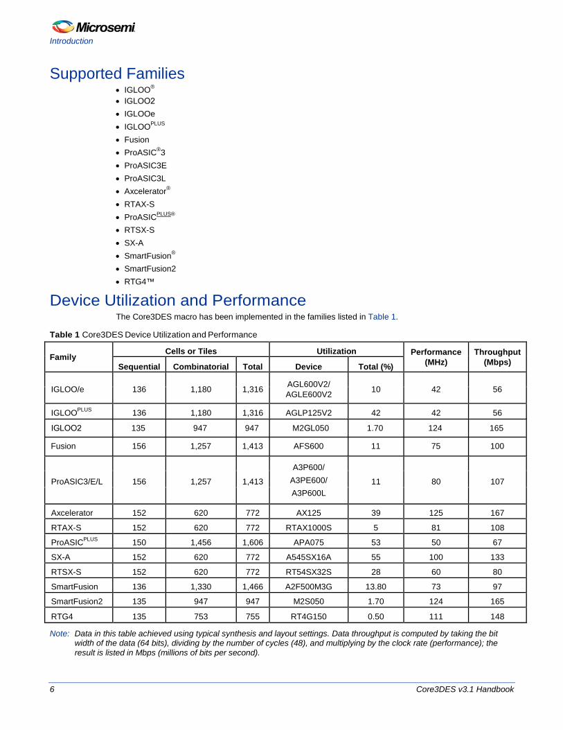
Device Utilization and Performance The Core3DES macro has been implemented in the families listed in Table 1.
Table 1 Core3DES Device Utilization and Performance
Family Cells or Tiles Utilization Performance
(MHz) Throughput
(Mbps) Sequential Combinatorial Total Device Total (%)
IGLOO/e 136 1,180 1,316 AGL600V2/ AGLE600V2 10 42 56
IGLOOPLUS 136 1,180 1,316 AGLP125V2 42 42 56
ProASIC3/E/L 156 1,257 1,413
A3P600/ A3PE600/ A3P600L
11 80 107
Axcelerator 152 620 772 AX125 39 125 167
RTAX-S 152 620 772 RTAX1000S 5 81 108
ProASICPLUS 150 1,456 1,606 APA075 53 50 67
SX-A 152 620 772 A545SX16A 55 100 133
RTSX-S 152 620 772 RT54SX32S 28 60 80
SmartFusion 136 1,330 1,466 A2F500M3G 13.80 73 97
SmartFusion2 135 947 947 M2S050 1.70 124 165
RTG4 135 753 755 RT4G150 0.50 111 148
Note: Data in this table achieved using typical synthesis and layout settings. Data throughput is computed by taking the bit width of the data (64 bits), dividing by the number of cycles (48), and multiplying by the clock rate (performance); the result is listed in Mbps (millions of bits per second).
6 Core3DES v3.1 Handbook
• IGLOO2
IGLOO2 135 947 947 M2GL050 1.70 124 165
Fusion 156 1,257 1,413 AFS600 11 75 100

Design Description
I/O Signals The port signals for the Core3DES macro are defined in Table 2 and illustrated in Figure 5. Core3DES has 202 I/ O signals (described in Table 2). Most arrayed ports are labeled with indices that begin with the number 1 (most significant bit) and ascend up to the width of the arrayed port (least significant bit, which is 64 for most of the arrayed ports in this core). The arrayed ports are labeled in this fashion to correspond with the nomenclature described in Federal Information Processing Standards Publication 46-3 (FIPS PUB 46-3). The only deviation from this nomenclature is the Key Select output bus, which descends from 1 down to 0.
Core3DES CLR
K[1:64]
PCHK
D[1:64]
KSEL[1:0]
QVAL
Q[1:64]
ED
CLK
EN
PERR
NRESET
Figure 5 Core3DES I/O Signal Diagram
Table 2 Core3DES I/O Signals Name Type Description
NRESET Input Active-low asynchronous reset
CLK Input System clock: reference clock for all internal Triple DES logic
EN Input Enable signal: set to '1' for normal continuous operation, set to '0' to pause
CLR Input Synchronous clear signal: set to '1' to clear logic at any time
ED Input Encrypt/Decrypt: '1' to Encrypt, '0' to Decrypt
PCHK Input Parity Check: set to '1' to enable parity checking of cipher key bits
K[1:64] Input Input Key: 64 bit (56 bits + 8 parity bits) cipher key input bus (time-multiplexed K1,K2,K3 sub-keys)
D[1:64] Input Data in: 64 bit data input bus
Q[1:64] Output Output Data out: 64 bits of ciphertext (for Encrypt operation, plaintext for Decrypt operation)
QVAL Output Q Valid: '1' indicates that valid Encrypt/Decrypt data is available on Q [1:64]
KSEL[1:0] Output Key Select: Selection bits for cipher key sub-keys K1, K2, and K3. When 00: K1 needs to be presented on the K[1:64] input bus, when 01: K2 needs to be presented on the K[1:64] input bus, when 10: K3 needs to be presented on the K[1:64] input bus.
PERR Output Parity Error: '1' indicates that a parity error has occurred on the K cipher key input bits
Core3DES v3.1 Handbook 7

Design Description
Parameters/Generics Core3DES has a parameter (Verilog) and generic (VHDL), described in Table 3, for configuring the RTL code. A parameter and generic is an integer type. This parameter/generic is mapped to configuration options in the SmartDesign Configuration window.
Table 3 Core3DES Configuration Parameter/Generic
Name Values Description
FAMILY 0 to 99 Must be set to match the supported FPGA family. IGLOO PLUS - 23 IGLOOe - 21 IGLOO - 20 Fusion - 17 ProASIC3L - 22 ProASIC3E - 16 ProASIC3 - 15 Axcelerator - 11 RTAX-S - 12 ProASICPLUS - 14 RTSX-S - 9 SX-A – 8 SmartFusion - 18 Smartfusion2 - 19 IGLOO2 - 24 RTG4 - 25
8 Core3DES v3.1 Handbook

Functional Block Description
Core3DES consists of four main blocks (shown in Figure 6). • Data schedule logic - computes the intermediate data values at each round of the DES algorithm. • Iteration state machine logic - keeps track of which round of the DES algorithm is currently in progress. • Key schedule logic - computes the intermediate keys at each round of the DES algorithm. • Parity check logic - checks for odd-parity compliance of the 56 bits of cipher key and issues an error signal
if parity is not correct.
Cipher Key
Parity Enable
Data In
Parity Error
Data OutData
ScheduleLogic
IterationState
Machine
KeySchedule
Logic
ParityCheckLogic
Figure 6 DES Algorithm Block Diagram
Core3DES v3.1 Handbook 9

Core3DES Operation
Selecting a Cipher Key Since there is only one cipher key K[1:64] input port and the Triple DES algorithm requires three 64-bit cipher subkeys (three 56-bit cipher sub-keys, less than 8 parity bits, per sub-key), the three cipher sub-keys must be presented in sequence on the same K[1:64] input port. The KSEL[1:0] output port must be decoded by the designer for use in external selection logic for each of the three 64-bit cipher sub-keys. Since the KSEL[1:0] output port may be connected to address lines of an external RAM or ROM device, there is an extra clock cycle of latency built into the Core3DES logic. In other words, when the KSEL[1:0] port changes value, the next cipher sub-key is not required immediately on the next rising edge of the clock, however; it will be required by the second rising edge of the clock. This is illustrated in “Encryption” on page 11 and “Decryption” on page 12.
Parity Checking If you want to use parity checking with the cipher key K[1:64] inputs, the PCHK input must be held at logic '1'. The parity checking logic determines whether or not an odd number of logic '1' values are present in each byte of the cipher key. This function can be disabled at any time by setting the PCHK input to logic '0'. Note: If parity checking is disabled by setting the PCHK input to logic '0,' the least significant bits of each
byte of the cipher key (K[8], K[16], K[24], K[32], K[40], K[48], K[56], and K[64]) can each be statically connected to either a logic '1' or logic '0' value, since they are the parity bits and will not be used (Figure 7).
PCHK PERR
81 6 24 32 40 48 56 64
K[1:64]
Parity CheckLogic
Figure 7 Key Parity Check
Core3DES v3.1 Handbook 10

Encryption
Encryption To begin the process of encrypting data, the following inputs are set: • K[1:64] is set to the first of three cipher sub-keys (ck1 in Figure 8) to encrypt the data. • D[1:64] is set to the plaintext data (d1 in Figure 8) to be encrypted. • ED is set to logic '1'. • EN is set to logic '1'. After 15 clock cycles of the EN input being held continuously at a logic '1' value, the KSEL[1:0] outputs change from '00' to '01', indicating that the second of three cipher sub-keys (ck2 in Figure 8) need to be presented on the K[1:64] inputs, which must be done by the rising clock edge of the start of clock cycle 17 (one complete clock cycle of slack is built into the Core3DES circuitry). After 31 clock cycles of the EN input being held at a logic '1', the KSEL[1:0] outputs changes from '01' to '10', indicating that the third of three cipher sub-keys (ck3 in Figure 8) need to be presented on the K[1:64] inputs, which must be done by the rising clock edge of the start of clock cycle 33. After 48 clock cycles of the EN input being held continuously at a logic '1' value, the QVAL signal transitions from logic '0' to logic '1' and remains valid for one clock cycle, indicating that valid ciphertext (encrypted) data (q1 in Figure 8) is available on the Q[1:64] outputs. Note that the encrypted data is only available during clock cycle 48, thus you must register or latch the data on Q[1:64], using the QVAL signal as a qualifying register enable or latch enable. As shown in Figure 8, continuous encryption is possible. For example, the second 64-bit plaintext data word (d2 in Figure 8) can be immediately encrypted by presenting d2 on the D[1:64] inputs by the rising clock edge of clock cycle 49 and by presenting the cipher sub-keys ck1, ck2, and ck3 in the sequence described earlier in this section.
d2
ck1
CLK
K[1:64]
D[1:64]
ED
EN
1 2 15 16cycle
Q[1:64]
QVAL
q1
ck1
d1
Don't care Undefined
01
3kc 2kc
01
1817
KSEL[1:0] 00 010100
31 32 3433 ... ... 47 48 5049...
00
Figure 8 Example Encryption Sequence
Core3DES v3.1 Handbook 11

Core3DES Operation
Decryption To begin the process of decrypting data, the following inputs are set: • K[1:64] is set to the third of three cipher sub-keys (ck3 in Figure 9) to decrypt the data. • D[1:64] is set to the ciphertext data (d1 in Figure 9) to be decrypted. • ED is set to logic '0'. • EN is set to logic '1'. After 15 clock cycles of the EN input being held continuously at a logic '1' value, the KSEL[1:0] outputs change from '10' to '01', indicating that the second of three cipher sub-keys (ck2 in Figure 9) must be presented on the K[1:64] inputs, which is done by the rising clock edge of the start of clock cycle 17 (one complete clock cycle of slack is built into the Core3DES circuitry). After 31 clock cycles of the EN input being held at a logic '1', the KSEL[1:0] outputs will change from '01' to '00', indicating that the first of three cipher sub-keys (ck1 in Figure 9) need to be presented on the K[1:64] inputs, which must be done by the rising clock edge of the start of clock cycle 33. Note that for decryption, the order in which the three cipher sub-keys are required differs from the encryption process (described in the previous section); cipher sub-key three is required first, cipher sub-key two is next, and cipher sub-key one is last. After 48 clock cycles of the EN input being held continuously at a logic '1' value, the QVAL signal transitions from logic '0' to logic '1' and remains valid for one clock cycle, indicating that valid plaintext (unencrypted data, shown as q1 in Figure 9) is available on the Q[1:64] outputs. Note that the decrypted plaintext data is only available during clock cycle 48, thus you must register or latch the data on Q[1:64] using the QVAL signal as a qualifying register enable or latch enable. As shown in Figure 9, continuous decryption is possible. For example, the second 64-bit ciphertext data word (d2 in Figure 9) can be immediately decrypted by presenting d2 on the D[1:64] inputs by the rising clock edge of clock cycle 49 and by presenting the cipher sub-keys ck3, ck2, and ck1 in the sequence described earlier in this section. After 16 clock cycles of the EN input being held continuously at a logic '1' value, the QVAL signal transitions from logic '0' to logic '1' and remains valid for one clock cycle, indicating that valid plaintext (unencrypted data shown as q1 in Figure 9) is available on the Q[1:64] outputs.
CLK
K[1:64]
D[1:64]
ED
EN
cycle
Q[1:64]
QVAL
KSEL[1:0]
d2
ck3
q1
ck3
d1
Don't care Undefined
01
ck2 ck1
0110 01000001
1 2 15 16 1817 31 32 3433... ... 47 48 5049...
Figure 9 Example Decryption Sequence
12 Core3DES v3.1 Handbook

Pause/Resume
Pause/Resume For normal operation, the EN input is held at a logic 1 value. The core can be paused by holding the EN input at a logic 0 value, indefinitely, as shown in Figure 10. To resume operation, the EN input must be brought back to a logic 1 value. This functionality applies to either encryption or decryption. Note that the ED input must remain at logic 1 throughout an entire encryption cycle, or at logic 0 throughout an entire decryption cycle; otherwise, unpredictable results on the Q[1:64] outputs occur. The pause/resume functionality is provided as an aid to you. The EN input would be held statically at a logic 1 value, and the data input needs to change every 48 clock cycles to encrypt the next block. After all blocks of data are encrypted, you would then need to hold the EN input at a logic 0 value, since if it is left at logic 1, data continues to be encrypted forever. When ready for the next blocks of data, you can then resume the encryption process by holding the EN input at a logic 1 value. Another possible use may be if you have an elastic buffer (FIFO) connected to the Q[1:64] outputs. If the FIFO is filling up with encrypted data faster than the encrypted data is being read out of the FIFO, you may wish to pause the Core3DES macro by setting the EN input to a logic 0 when the full or almost-full flag logic from the FIFO is active. When the FIFO full or almost-full flag logic clears, the Core3DES macro can then resume operation by again setting the EN input to a logic 1 value.
ck1
d2
CLK
K[1:64]
D[1:64]
ED
EN
12 3a 45 ... cycle
ck1
d1
Don't care Undefined
3b 3c
cycle 3 "paused"
Q[1:64]
QVAL
q1
01 01KSEL[1:0] 00 0100 10 00
15 16 1817 31 32 3433... 47 48 5049...
ck2 ck3
Figure 10 Example Encryption Pause/Resume Sequence
Core3DES v3.1 Handbook 13

Core3DES Operation
Clear/Abort At any point in the process of encrypting or decrypting data, you can abort the current operation by setting the CLR input to logic 1. This clears all current calculations with the key schedule and data schedule logic. You can then immediately begin to use a different cipher key and data input on the very next cycle, as shown in Figure 11. The clear/abort functionality is useful when you want to change the cipher key, possibly in the middle of an encryption or decryption sequence. You are able to immediately halt the current operation simply by holding the CLR input at a logic 1 value for at least one clock cycle, and commence immediately on the following clock cycle with a new cipher key and/or new data. If the Core3DES macro is integrated into a system containing a processor, the processor may want to abort the encryption or decryption operation for some specific event (for example, low or failing power condition).
internal logic cleared/flushed; cipher key (ck1) and data (d1)
calculations aborted
encrypted data using cipher keys (ck1', ck2', ck3') and data (d2)
d3
ck1'
ED
EN
1 2 15 16
Q[1:64]
QVAL
q2
ck1'
d2
Don't care Undefined
01
ck2' ck3'
01
1817
KSEL[1:0] 00 010100
31 32 3433... ... 47 48 5049...
00
CLR
CLK
K[1:64]
D[1:64]
123 cycle
ck1
d1
Figure 11 Example Encryption Abort Sequence
Modes of Operation Core3DES is implemented using the TECB (TDEA Electronic Codebook) mode of operation, per ANSI Standard X9.52. Depending on the application, other modes of operation for Triple DES may be desirable. For this reason, Microsemi provides example VHDL and Verilog source code for the TCBC (TDEA Cipher Block Chaining), TCFB (TDEA Cipher Feedback), and TOFB (TDEA Output Feedback) modes. For detailed information on specific modes of operation, refer to ANSI Standard X9.52.
14 Core3DES v3.1 Handbook

Tool Flows and Testbench Operation
License Core3DES is licensed two ways: Obfuscated and register transfer level (RTL).
Obfuscated Complete RTL code is provided for the core, allowing the core to be instantiated with SmartDesign. Simulation, Synthesis, and Layout can be performed within Libero® System-on-Chip (SoC). The RTL code for the core is obfuscated and the some of the testbench source files are not provided; they are precompiled into the compiled simulation library instead.
RTL Complete RTL source code is provided for the core and testbenches.
SmartDesign Core3DES is preinstalled in the SmartDesign IP Deployment design environment. The core can be configured using the configuration GUI within SmartDesign, as shown in Figure 12. For information on using SmartDesign to instantiate and generate cores, refer to the Using the Using DirectCore in Libero SoC User Guide or Libero Online Help.
Figure 12 Core3DES Configuration Window in SmartDesign
Simulation Flows The User Testbench for Core3DES is included in all releases. To run simulations, select the User Testbench flow within CoreConsole and click Save & Generate on the Generate pane. The User Testbench is selected through the Core Testbench Configuration GUI. When SmartDesign generates the Libero project, it installs the user testbench files. To run the user testbench, set the design root to the Core3DES instantiation in the Libero design hierarchy pane and click Simulation in the Libero Design Flow window. This will invoke ModelSim® and automatically run the simulation.
Core3DES v3.1 Handbook 15

Tool Flows and Testbench Operation
Synthesis in Libero To run synthesis on the core with the parameter/generic set in SmartDesign, set the design root appropriately and click the Synthesis icon in Libero Project Flow window. The Synthesis window appears, displaying the Synplicity® project. If using Verilog, set Synplicity to use the Verilog 2001 standard. Run Synplicity.
Place-and-Route in Libero After running Synthesis, click Layout in Libero to invoke Designer. Core3DES requires no special place and-route settings.
16 Core3DES v3.1 Handbook

Testbench Operation
An example user testbench is included with the obfuscated and RTL releases of Core3DES. The obfuscated and RTL releases provide the precompiled ModelSim format, as well as the source code for the user testbench to ease the process of integrating and verifying the Core3DES macro into a design. The user testbench includes a simple example design that serves as a reference for users that want to implement their own designs. The source code for each user testbench includes example support routines to aid the user in testing the Core3DES macro. Refer to the comments in the user testbench source code for details on the support routines (tasks for Verilog testbenches, functions and procedures for VHDL testbenches.) Using the supplied testbench as a guide, you can easily customize the verification of the core by adding or removing any of the tests listed in NIST Special Publication 800-20 or by adding any custom test cases.
Core3DES v3.1 Handbook 17

Ordering Information
Ordering Codes Order Core3DES through your local Microsemi sales representative. Use the following number convention when ordering: Core3DES-XX, where XX is listed in Table 4.
Table 4 Ordering Codes XX Description OM RTL for Obfuscated RTL— multiple use license RM RTL for RTL source — multiple-use license
Export Restrictions Core3DES is subject to export controls and is licensable under the U.S. Department of Commerce's Export Administration Regulations, the U.S. Department of State's International Traffic in Arms Regulations, or other laws, government regulations, or restrictions. Microsemi is currently in the process of obtaining additional permissions to ship Core3DES to a wider audience. The licensee will not import, export, re-export, divert, transfer, or disclose Core3DES without complying strictly with the export control laws and all legal requirements in the relevant jurisdictions, including and without limitation, obtaining the prior approval of the U.S. Department of Commerce or the U.S. Department of State, as applicable.
Core3DES v3.1 Handbook 18

List of Changes
The following table lists critical changes that were made in each revision of the document. Date Change Page February 2015 Updated for Core3DES v3.1 release. NA
March 2009 Initial release. NA
Core3DES v3.1 Handbook 19

Product Support
Microsemi SoC Products Group backs its products with various support services, including Customer Service, Customer Technical Support Center, a website, electronic mail, and worldwide sales offices. This appendix contains information about contacting Microsemi SoC Products Group and using these support services.
Customer Service Contact Customer Service for non-technical product support, such as product pricing, product upgrades, update information, order status, and authorization.
From North America, call 800.262.1060 From the rest of the world, call 650.318.4460 Fax, from anywhere in the world 650. 318.8044
Customer Technical Support Center Microsemi SoC Products Group staffs its Customer Technical Support Center with highly skilled engineers who can help answer your hardware, software, and design questions about Microsemi SoC Products. The Customer Technical Support Center spends a great deal of time creating application notes, answers to common design cycle questions, documentation of known issues and various FAQs. So, before you contact us, please visit our online resources. It is very likely we have already answered your questions.
Technical Support For Microsemi SoC Products Support, visit http://www.microsemi.com/products/fpga-soc/design-support/fpga-soc-support.
Website You can browse a variety of technical and non-technical information on the Microsemi SoC Products Group home page, at http://www.microsemi.com/soc/.
Contacting the Customer Technical Support Center Highly skilled engineers staff the Technical Support Center. The Technical Support Center can be contacted by email or through the Microsemi SoC Products Group website.
Email You can communicate your technical questions to our email address and receive answers back by email, fax, or phone. Also, if you have design problems, you can email your design files to receive assistance. We constantly monitor the email account throughout the day. When sending your request to us, please be sure to include your full name, company name, and your contact information for efficient processing of your request. The technical support email address is [email protected].
My Cases Microsemi SoC Products Group customers may submit and track technical cases online by going to My Cases.
Core3DES v3.1 Handbook 20

ITAR Technical Support
Outside the U.S. Customers needing assistance outside the US time zones can either contact technical support via email ([email protected]) or contact a local sales office. Sales office listings can be found at www.microsemi.com/soc/company/contact/default.aspx.
ITAR Technical Support For technical support on RH and RT FPGAs that are regulated by International Traffic in Arms Regulations (ITAR), contact us via [email protected]. Alternatively, within My Cases, select Yes in the ITAR drop-down list. For a complete list of ITAR-regulated Microsemi FPGAs, visit the ITAR web page.
Core3DES v3.1 Handbook 21

50200158.2/02.15
Microsemi Corporation (Nasdaq: MSCC) offers a comprehensive portfolio of semiconductor and system solutions for communications, defense & security, aerospace and industrial markets. Products include high-performance and radiation-hardened analog mixed-signal integrated circuits, FPGAs, SoCs and ASICs; power management products; timing and synchronization devices and precise time solutions, setting the world’s standard for time; voice processing devices; RF solutions; discrete components; security technologies and scalable anti-tamper products; Power-over-Ethernet ICs and midspans; as well as custom design capabilities and services. Microsemi is headquartered in Aliso Viejo, Calif., and has approximately 3,400 employees globally. Learn more at www.microsemi.com.
© 2015 Microsemi Corporation. All rights reserved. Microsemi and the Microsemi logo are trademarks of Microsemi Corporation. All other trademarks and service marks are the property of their respective owners.
Microsemi Corporate Headquarters One Enterprise, Aliso Viejo, CA 92656 USA Within the USA: +1 (800) 713-4113 Outside the USA: +1 (949) 380-6100 Sales: +1 (949) 380-6136 Fax: +1 (949) 215-4996 E-mail: [email protected]
Microsemi makes no warranty, representation, or guarantee regarding the information contained herein or the suitability of its products and services for any particular purpose, nor does Microsemi assume any liability whatsoever arising out of the application or use of any product or circuit. The products sold hereunder and any other products sold by Microsemi have been subject to limited testing and should not be used in conjunction with mission-critical equipment or applications. Any performance specifications are believed to be reliable but are not verified, and Buyer must conduct and complete all performance and other testing of the products, alone and together with, or installed in, any end-products. Buyer shall not rely on any data and performance specifications or parameters provided by Microsemi. It is the Buyer’s responsibility to independently determine suitability of any products and to test and verify the same. The information provided by Microsemi hereunder is provided “as is, where is” and with all faults, and the entire risk associated with such information is entirely with the Buyer. Microsemi does not grant, explicitly or implicitly, to any party any patent rights, licenses, or any other IP rights, whether with regard to such information itself or anything described by such information. Information provided in this document is proprietary to Microsemi, and Microsemi reserves the right to make any changes to the information in this document or to any products and services at any time without notice.