Embed Size (px)
Citation preview

Copyrighted
By
Vahid Atar Akhavan
2011

The Dissertation Committee for Vahid Atar Akhavan certifies that this is the
approved version of the following dissertation:
Photovoltaic Devices Based on
Cu(In1-xGax)Se2 Nanocrystal Inks Committee: ______________________________ Brian A. Korgel, Supervisor ______________________________ John G. Ekerdt ______________________________ Charles B. Mullins ______________________________ Christopher J. Ellison ______________________________ Ananth Dodabalapur

Photovoltaic Devices Based on
Cu(In1-xGax)Se2 Nanocrystal Inks
by:
Vahid Atar Akhavan, B.S.
Dissertation
Presented to the Faculty of the Graduate School of
The University of Texas at Austin
in Partial Fulfillment
of the Requirements
for the Degree of
Doctor of Philosophy
The University of Texas at Austin
August 2011

Dedication
For My Parents

v
Acknowledgments
I find myself to be extremely lucky. I have always been surrounded by
exceptional individuals. It is remarkable how much of my knowledge I owe to them.
First and foremost, I would like to thank my advisor, Dr. Brian Korgel, for
providing the inspiration, knowhow and tools necessary to pursue my work for the past
five years. I will always be grateful for the opportunity. Brian is passionate about his
work and his work ethic is contagious. I hope he keeps discovering and developing new
technologies. My work would not have been possible without him.
Past and present Korgelites have been instrumental to my work. I learned many
things from them, and the diversity present in the group has introduced me to many new
concepts. I am grateful to be associated with such an exceptional group of people. Brian
Goodfellow and Matthew Panthani were the source of ideas and the sanity check for the
photovoltaics project. In hindsight, we had many crazy ideas. It was an honor to be
considered only a third of a competent graduate student when lumped in with these guys.
Danielle Smith, Reken Patel, Damon Smith, Andrew Heitsch, Dr. Colin Hessel, Hsing-
Yu Tuan, Doh Lee, Bonil Koo, Dayne Fanfair, and Tripp Davidson were my mentors. I
am grateful for their support, optimism, and daily encouragement. Andy, Colin and
Reken were kind enough to get me involved with surface characterization of silicon
nanostructures, and I thank them for their decision. Aaron Chockla, Kate Collier, Justin
Harris, Vince Holmberg, Michael Rasch, Catherine Shipman, Chet Steinhagen and Dr.
Jose-Luis Hueso Martos were indispensable colleagues. Recent Korgelites Carl Jackson
Stolle and Taylor Harvey have been dedicated researchers and great help over the past
couple of months. I hope they continue working on the photovoltaic project and make

vi
great discoveries. I have thoroughly enjoyed my friendship with all the Korgelites and I
hope we remain close friends in the future. I wish all of them the best of luck as they
continue on.
I was also honored to work with some bright undergraduates and they all had a
positive impact on my work. I would like to thank all of them. It was a privilege to teach
them and learn from them. Special thanks goes to Dariya Reid and Danny Hellebusch,
they were great help at the most critical parts of my work. They are bright students and I
know they will do great work.
Dr. Paul Barbara, Dr. Ananth Dodabalapur, Dr. Allen Bard, Dr. Johanna Schmidt,
Takuji Adachi, Dr. Heechang Ye, Hyun Park, Dr. Lawrence Dunn and Dr. Chris
Lombardo were closely involved with the photovoltaics project. Dr. David Vanden Bout,
Micah Glaz and David Ostrowski collected the light beam induced current microscopy
(LBIC) maps of photovoltaic devices and these measurements were crucial to our
understanding of device performance. I am grateful for all their support.
Most importantly, near and extended family had a great impact on my
development as an individual and a scientist. Their selfless help and amazing precedence
gave me the courage to be where I am today. My grandmother, Robab Azadhosseini, and
my sisters, Neda and Mina, were the reasons I pursued my Ph.D. and why I had the
stamina to push through. I would have had an empty and unfulfilling existence without
them. My uncles, Reza Aghili, Mohammad Aghili, Ali Aghili, Morteza Akhavan and
Habib Akhavan, were like fathers to me. They helped with my family and financial
obligations, allowing me to concentrate on my studies. My cousins, Ali and Masoud

vii
Mazoochi, were like my brothers, and pushed me to be the best I could be. Finally,
Mahsa Mansouri gave me the audacity to think of a brighter future.
I hope everyone will benefit from my work. If I achieve something beyond my
simple existence, it is because I was lucky to know such exceptional people.

viii
Preface
Gloomy predictions of a future with energy shortages or a compromised
environment are common for today’s analysts and pundits. A future of 10 billion,
relatively rich humans living comfortably on one planet is thought of as science fiction.
The issue at the heart of such predictions is how closely quality of life has been tied to
access to cheap and abundant energy resources. It is a remarkable correlation how richer
societies need more energy and how development of new energy resources is followed by
improvements in quality of life. With today’s energy markets stretched to the limit, many
fear promotion of 1 billion people, living today at sustenance levels, to middle class will
create havoc on the environment or create shortages for wealthier populace of earth.
Creating an egalitarian society for everyone will be a planetary challenge during my
lifetime and an admirable goal. To see the future as a Malthusian trap is to discount the
ingenuity of man (and woman) and ten millennia of precedence. I hope the work
presented here will come to fruition and contribute to a brighter future.

ix
Photovoltaic Devices Based on
Cu(In1-xGax)Se2 Nanocrystal Inks
Publication No.___________
Vahid Atar Akhavan, Ph.D.
The University of Texas at Austin, 2011
Supervisor: Brian A. Korgel
Thin film copper indium gallium selenide (CIGS) solar cells have exhibited single
junction power conversion efficiencies above 20% and have been commercialized. The
large scale production of CIGS solar cells, however, is hampered by the relatively high
cost and poor stoichiometric control of coevaporating tertiary and quaternary
semiconductors in high vacuum. To reduce the overall cost of production, CIGS
nanocrystals with predetermined stoichiometry and crystal phase were synthesized in
solution.
Colloidal nanocrystals of CIGS provide a novel route for production of electronic
devices. Colloidal nanocrystals combine the well understood device physics of inorganic
crystalline semiconductors with the solution processability of amorphous organic
semiconductors. This approach reduces the overall cost of CIGS manufacturing and can
be used to fabricate solar cells on flexible and light-weight plastic substrates.

x
As deposited CIGS nanocrystal solar cells were fabricated by ambient spray-
deposition. Devices with efficiencies of 3.1% under AM1.5 illumination were fabricated.
Examining the external and internal quantum efficiency spectrums of the devices reveal
that in nanocrystal devices only the space charge region is actively contributing to the
extracted photocurrent. The device efficiency of the as-deposited nanocrystal films is
presently limited by the small crystalline grains (≈ 15 nm) in the absorber layer and the
relatively large interparticle spacing due to the organic capping ligands on the nanocrystal
surfaces. Small grains and large interparticle spacing limits high density extraction of
electrons and holes from the nanocrystal film. A Mott-Schottky estimation of the space
charge region reveals that only 50 nm depth of the nanocrystalline absorber is effectively
contributing to the photogenerated current.
One strategy to improve charge collection involves increased space charge region
for extraction by vertical stacking of diodes. A much longer absorption path for the
photons exists in the space charge region with the stacked devices, increasing the
probability that the incident radiation is absorbed and then extracted. This method
enables an increase in the collected short circuit current. The overall device efficiency,
however, suffers with the increased series resistance and shunt conductance of the device.
Growth of nanocrystal grains was deemed necessary to achieve power conversion
efficiencies comparable to vapor deposited CIGS films.
Simple thermal treatment of the nanocrystal layers did not contribute to the
growth of the crystalline grain size. At the same time, because of the loss of selenium and
increased trap density in the absorber layer, there was a measurable decrease in device
efficiency with thermal processing.

xi
For increased grain size, the thermal treatment of the absorber layer took place in
presence of compensating amounts of selenium vapor. The process of selenization, as it
is called, took place at 500°C in a graphite box and led to an increase of the grain size
from 15 nm to several microns in diameter. Devices with the increased grain size yielded
efficiencies up to 5.1% under AM1.5 radiation. Mott-Schottky analysis of the selenized
films revealed a reduction in doping density and a comparable increase in the space-
charge region depth with the increased grain size. The increased collection combined
with the much higher carrier mobility in the larger grains led to achieved Jsc values
greater than 20 mA/cm2.
Light beam induced current microscopy (LBIC) maps of the devices with
selenized absorber layers revealed significant heterogeneity in photogenerated current.
Distribution of current hotspots in the film corresponded with highly selenized regions of
the absorber films. In an effort to improve the overall device efficiency, improvements in
the selenization process are necessary. It was determined that the selenization procedure
is dependent on the selenization temperature and processing environment. Meanwhile,
the reactor geometry and nanocrystal inks composition played important roles in
determining selenized film morphology and the resulting device efficiency. Further work
is necessary to optimize all the parameters to improve device efficiency even further.

xii
Table of Content
List of Tables…………………………………………………………………………....xvi
List of Figures……………………………………………………………………….….xvii
Chapter 1: Introduction……………………………………………………………………1
1.1 Overview of Solar Cell Market………………..………………………………1
1.2 Alternatives to Silicon…………………………………………………………2
1.3 Third Generation Photovoltaics and the Printed Inorganic Thin Film Solar
Cell ……………………………………………………………………………3
1.4 Nanocrystal Ink Formulation………………………………………………….4
1.5 CIGS Nanocrystal Inks……………………………………………….............5
1.6 References……………………………………………………………………10
Chapter 2: Spray-Deposited CuInSe2 (CIS) Nanocrystal Photovoltaics…………………13
2.1 Introduction…………………………………………………………………..13
2.2 Experimental Details…………………………………………………………15
2.2.1 Chemicals…………………………………………………………..15
2.2.2 CIS nanocrystal synthesis………………………………………….16
2.2.3 Materials Characterization…………………………………………17
2.2.4 PV device fabrication and testing………………………………….18
2.3 Results and Discussion………………………………………………………19
2.3.1 CIS nanocrystals…………………………………………………...19

xiii
2.3.2 PV devices fabricated by spray-deposition of CIS nanocrystals......21
2.3.3 Replacement of the Mo back contact with Au……………….........22
2.3.4 Influence of CIS layer thickness on device efficiency……..….......23
2.3.5 Improved efficiency by device stacking…………………..….........27
2.4 Conclusions…………………………………………………………………..31
2.5 Notes and References………………………………………………………...32
Chapter 3: Thickness-Limited Performance of CuInSe2 Nanocrystal PVs……………...34
3.1 Introduciton…………………………………………………………………..34
3.2 Experimental…………………………………………………………………36
3.2.1 Nanocrystal inks……………………………………………………36
3.2.2 Material characterization…………………………………………..37
3.2.3 PV device fabrication………………………………………………37
3.2.4 PV device testing…………………………………………………..38
3.3 Results and Discussion………………………………………………………39
3.3.1 CuInSe2 nanocrystal inks………………………………………….39
3.3.2 PV device fabrication………………………………………………40
3.3.3 Diode behavior in the dark and light……………………………….41
3.3.4 Device performance limitation…………………………………….44
3.3.5 Impedance spectroscopy…………………………………………...47
3.4 Conclusion…………………………………………………………………...49
3.5 Notes and References………………………………………………………..50
Chapter 4: Improved Device Performance with Modification to Synthetic Chemistry and
Low-Temperature Treatment of Nanocrystal Inks……………………………………....52

xiv
4.1 Introduction…………………………………….…………………………….52
4.2 Experimental Details………………………………………....………………54
4.2.1 Materials…………………………….……………………………..54
4.2.2 CuInSe2 nanocrystal synthesis……………………………………..55
4.2.3 PV device fabrication………………………………………………57
4.2.4 Characterization……………………………………………………58
4.3 Changes to Nanocrystal Synthesis………………………….………………..59
4.4 Removing Capping Ligand through Thermal and Chemical Treatment….....64
4.5 Summary……………………………………………………………………..69
4.6 Notes and References………………………………………………………...70
Chapter 5: Selenization and Grain Growth of CIGS Nanocrystals………………………73
5.1 Introduction…………………………………………………………………..73
5.2 Experimental…………………………………………………………………75
5.2.1 Materials…………………………………………………………...75
5.2.2 CuIn1-xGaxSe2 (CIGS) nanocrystal synthesis………………………75
5.2.3 CuInS2 nanocrystal synthesis………………………………………76
5.2.4 PV device fabrication………………………………………………77
5.2.5 Characterization…………………………………………………....79
5.3 Selenization of CIGS nanocrystals…………………………………………..80
5.3.1 Variation in selenization…………………………………………...87
5.3.2 Characterization of the amorphous layer…………………………..97
5.3.3 Formation of MoSe2………………………………………………101
5.4 High Efficiency Selenized Nanocrystal CIGS Devices…………………….102

xv
5.4.1 Role and purity of CdS layer……………………………………..105
5.4.2 Retaining flexibility in device architecture……………………….106
5.4.3 Engineering electronic bandgap based on Ga content of nanocrystal
inks………………………………………………………………..108
5.5 Summary……………………………………………………………………109
5.6 Notes and References…………………………………………………….....111
Chapter 6: Conclusion…………………………………………………………………..113
6.1 Notes and References…………………………………………………….....118
Bibilography…………………………………………………………………………....119
Vita……………………………………………………………………………………...127

xvi
List of Tables
Table 1.1. Summary of the reported device efficiencies of PVs with nanocrystal-
based absorber layers deposited without high temperature or vacuum
processing. Reproduced with permission from Akhavan et. al. ………….6
Table 2.1. Summary of device characteristics obtained from stacked junction spray-
deposited CIS nanocrystal devices with transparent back contacts…..….29
Table 3.1. Diode performance parameters for the highest efficiency PVs………….42
Table 5.1. Measured composition of nanocrystals based on ICP-ms analysis for
targeted x in Cu(In1-xGax)Se2 relative to the concentration of Cu present
and the best device characteristics based on selenized films of the
nanocrystals……………………………………………………………..102

xvii
List of Figures
Figure 1.1. (a) Photogrpah of a CIGS nanocrystal ink; (b) a large-area scanning
electron micrograph of a nanocrystal film deposited by spray-coating the
ink; (c) transmission electron micrograph of CIGS nanocrystals; and (d) an
illustration of a nanocrystal, that depicts the inorganic crystalline core
coated by the organic capping ligand layer that stabilizes the
nanocrystals……………………………………………………………….7
Figure 1.2. (Top panel) Solar cells made by spray-coating CIGS nanocrystal inks on
various substrates: on glass with either (top left) molybdenum or (top
middle) gold back contacts, and (top right) on plastic (Kapton). (Middle)
Schematic showing the layer structure of a PV device; in this case, light is
absorbed by the CIGS layer and electron-hole separation leads to
photogenerated power. (Bottom) An example of the device characteristics
obtained from a PV device made with a CuInSe2 nanocrystal ink. The
open circuit voltage (Voc) and fill factor (FF) of the device are similar to
those of commercially available CIGS cells; however, the short circuit
current density (Jsc) is only 25% of the expected value for an absorber
material with this bandgap, resulting in the low device efficiency (η)……8
Figure 1.3. (a) Photograph of the spray deposition of a nanocrystal ink into a PV
device. (b) Cross-sectional SEM image of a completed device…………..9

xviii
Figure 2.1. (a,b) TEM images of CIS nanocrystals; (c) an SEM image of a film of CIS
nanocrystals spray-deposited from a toluene dispersion; (d) XRD pattern
of CIS nanocrystals indexed to chalcopyrite CIS (PDF#97-006-8928).
The inset in (d) is the average Cu, In and Se composition determined by
EDS of a field of nanocrystals…………………………………………...20
Figure 2.2. (a) SEM image of a cross-section of the PV device built using the
conventional device architecture with spray coated CIS nanoparticle layer
in place of vapor deposited CIS layer and (b) the I-V characteristics and
power conversion efficiency of a typical PV device with this structure…21
Figure 2.3. (Top) Photographs of PVs fabricated by spray depositing CIS nanocrystals
on various substrates: (top left and right) glass and (top, middle) plastic
(kapton). (Bottom) Illustration of the device layer structure as viewed
from the top and from the side…………………………………………...22
Figure 2.4. I-V characteristics of spray-deposited CIS nanocrystal PVs with gold back
contacts on (a) soda lime glass and (b) plastic (kapton). The power
conversion efficiencies (PCE) were measured under AM1.5
illumination………………………………………………………………23
Figure 2.5. Device characteristics measured for PVs made with spray-deposited CIS
nanocrystal layers of varying thickness. AM1.5 is the PCE under AM1.5
illumination, OCV is the open circuit voltage, and SCJ is the short circuit
current density……………………………………………………………24
Figure 2.6. (a) UV-vis-NIR absorbance spectra of a 200 nm thick CIS nanoparticle
film on a quartz substrate and the corresponding fraction of incident light

xix
that is absorbed. (b) External and internal quantum efficiency (EQE and
IQE) of a PV device made with a spray-deposited CIS nanocrystal layer.
EQE is determined from the incident photon conversion efficiency (IPCE)
spectra, which is a measure of short circuit current as a function of light
wavelength. The IQE is then determined from the EQE by accounting for
the fraction of light that is absorbed by the CIS layer at each wavelength
(i.e., the absorbance spectra). It should be noted that these IQE
calculations do not account for additional absorption in the active layer
that might occur due to internal reflections within the device, and the
absorbance of light by CdS at wavelengths of 500 nm and less are also not
accounted for in the IQE calculation……………..……………………..26
Figure 2.7. (a) I-V characteristics of a device prepared with a transparent ITO back
contact, and (b) the fraction of the incident light absorbed and transmitted
by the device on ITO determined from the UV-vis absorbance spectra of
the device………………………………..………………………………27
Figure 2.8. I-V characteristics of nearly transparent devices prepared with ITO back
and top contacts placed in a stacked device configuration………….….28
Figure 2.9. I-V characteristics of two CIS nanocrystal PVs measured independently
and in a stacked configuration under AM1.5 illumination………..……29
Figure 2.10. I-V characteristics of typical diodes used for the stacked structure devices
that were prepared on Au and ITO back contacts. Measured data (open
circles) were modeled (solid lines) using Eqn (1). The best fit of Eqn (1)
to the data gives the diode parameters tabulated in the inset……………30

xx
Figure 3.1. (A, B) TEM images and (C) XRD of the CuInSe2 nanocrystals. The
diffraction peaks in (C) are indexed to chalcopyrite CuInSe2 (PDF#97-
006-8928). The inset shows the chalcopyrite unit cell of CuInSe2: red, blue
and green spheres correspond to copper, indium and selenium atoms,
respectively………………………………………………………………40
Figure 3.2. I-V characteristics of a device with power conversion efficiency of 3.1%
under AM1.5 illumination. Dark conditions (black) and under AM1.5
irradiation (red). The device parameters are obtained by a best fit of Eqn
(1) (solid lines) to the data (). The parameters from the best fit are listed
in table 3.1……………………………………………………………….41
Figure 3.3. (A) I-V measurements of a CuInSe2 nanocrystal PV device with a
crossover between the light and the dark curves. Using light with
wavelength higher than 515 nm, the crossover is still present. By using
only low energy photons above 630 nm wavelength, however, the cross
over between the dark and light curves is eliminated. (B) Spectra of light
used for each illuminated measurement…………………………………43
Scheme 3.1. Band alignment of CuInSe2/CdS/ZnO heterojunction with or without the
photo-doping of the CdS buffer layer. Modified from Poduv, et. al…...44
Figure 3.4. (A) I-V measurements of devices with varying thickness of spray
deposited CuInSe2 nanocrystal film and (B) calculated device parameters
associated with these devices……………………………………………45
Figure 3.5. (A) IPCE measurements of a set of devices with different thicknesses of
the CuInSe2 nanocrystal film thickness shows similar trend between the

xxi
different thicknesses. (B) Internal quantum efficiency data of the same
devices reveals how thinner devices extract photogenerated carriers at a
better efficiency………………………………………………………..46
Figure 3.6. (A) Device architecture used for C-V measurements consists of a
simplified junction. (B) One diode model considered for this type of
junction to analyze the impedance data. (C) Sample Nyquist plot
illustrating the response of the junction at a certain bias; inset provides the
parameters gathered from the model fit (solid line) for the equivalent
circuit to the raw data (marked by ). (D) Linear plot of inverse square
capacitance of the junction versus applied voltage across the junction,
inset provides the gathered parameters based on Mott-Schottky
approximation. Area of this device was isolated to 8 mm2. (E) I-V
characteristics of this junction show that it shows a very similar response
to the more complex conventional devices, inset lists the device
parameters..............................................................................................49
Figure 4.1. TEM of CuInSe2 nanocrystals, composition of nanocrystal inks as
measured by ICP-ms analysis and IV response of devices prepared by
using the nanocrystal inks. (A-B) Correspond with results gathered from
an elemental-Se reaction using Acros oleylamine, (C-D) correspond with
results gathered from a TBP:Se reaction using Acros oleylamine, and (E-
F) correspond with an elemental-Se reaction using TCI oleylamine. TEM
images courtesy of Matthew Panthani and C. Jackson Stolle……….…61

xxii
Figure 4.2. (A) Efficiency and (B) short circuit current density of devices prepared
from CuInSe2 nanocrystal inks synthesized by hot injection of TBP:Se at
different injection temperatures. (C) Measured doping density (NA) based
on Mott-Schottky analysis of the junction marked by () and the
calculated depletion width marked by (), marked on the right axis. (D)
Composition of the resulting nanocrystal inks as measured by ICP-ms
analysis, In:Cu ratio is marked by () and the Se:Cu ratio is marked by
()…………………………………………………………………….…63
Figure 4.3. Device characteristics of nanocrystalline CuInSe2 PVs. The nanocrystal
layers were treated with different concentrations of hydrazine in
acetonitrile for 60 minutes after spray casting and before CdS
deposition………………………………………………………………...67
Figure 4.4. (A) Device characteristics of CuInSe2 nanocrystal devices baked in a
vacuum oven at 200°C for variety of lengths of time. (B) Impedance
response of the resulting diodes baked for different lengths of time. (C)
Change in series resistance of the diode in dark conditions and under
illumination with AM 1.5 radiation after baking for different lengths of
time...........................................................................................................69
Figure 5.1. (A) Side view and (B) cross-sectional view of the selenization box used for
sintering of nanocrystal layers. The cylinder is capped with the plug to
ensure buildup of a selenium partial pressure. (C) Tube furnace used for
heating the selenization box……………………………………………...82

xxiii
Figure 5.2. (A) XRD pattern of CIS films before and after selenization, matching well
with the estabulished crystal structure of CuInSe2 (PDF#97-006-8928) (B)
SEM image of cross section of an as-deposited CuInSe2 film and (C)
selenized CuInSe2 film…………………………………………………...83
Figure 5.3. (A) Spatial and (B) cross section SEM image of selenized CuInSe2 film.
(C) Shows the response of light beam induced current microscopy (LBIC)
measurements and (D) flouresence microscopy image of device prepared
with the selenized film. LBIC data courtesy of Micah Glaz……………..84
Figure 5.4. (A) IV response of nanocrystalline and selenized CuInSe2 films. The
nanocrystal device (denoted in blue) was built on Au back contacts, and
the selenized device (denoted in red) was built based on the Mo back
contacts. (B) Mott-Schottky response of the nanocrystal and selenized
devices denotes a decrease in the doping density of the absorber layer with
increasing grain sizes. The decrease in the doping density, combined with
the improved mobility, increases the probability of collection for the
photogenerated carriers. (C) Series resistance and (D) shunt resistance of
the two diodes at different applied potentials……………………………86
Figure 5.5. SEM of the surface and the cross-section of selenized CuInS2 nanocrystal
films at different temperatures, (A-B) 350°C, (C-D) 400°C, and (E-F)
500°C. (G-H) Correspond to CuInS2 particles selenized at 500°C but the
as-deposited nanocrystal film was treated with hydrazine solution before
selenization………………………………………………………………90

xxiv
Figure 5.6. SEM of the surface of selenized CIGS nanocrystals at 500°C (A-B) inside
a leaky box or (C-D) in a tightly sealed box……………………………..92
Figure 5.7. TEM images of as-synthesized nanocrystals, surface and cross-sectional
SEM of the selenized films and IV response of the fabricated devices with
500°C selenized nanocrystal absorber layers. (A-D) high indium excess
CuInSe2 nanocrystal grains, (E-H) lower indium excess CuInSe2
nanocrystal grains, and (I-L) indium deficient CuInS2 nanocrystal grains.
TEM images courtesy of C. Jackson Stolle……………………………...95
Figure 5.8. (A) Surface SEM and (B) cross-sectional SEM of CuInS2 nanopraticles
baked at 500°C and then selenized at 500°C…………………………….96
Figure 5.9. (A) Cross-sectional SEM image of a selenized CIGS film, coverage of the
amorphous layer on the surface of the selenized crystals limits the
performance of the fabricated devices. (B) XPS spectrum of the as-
selenized CIGS layer before and after Ar sputtering. Sputtering of the
surface layer with high energy Ar exposes the crystalline structure
underneath the surface layer of carbon and selenium. The underlying layer
had similar composition to that of the starting nanocrystals……………..98
Figure 5.10. High resolution XPS scans of In 3d5/2, C 1s and Se 3d regions of CIGS
films before and after selenization at 500°C. Post-baking of the selenized
absorber layers for 60 minutes at different temperatures removed some
excess elemental selenium but a majority of the carbonaceous material
remained. All the peak intensities are normalized for easier viewing….100

xxv
Figure 5.11. (A) EDS line-scan across the (B) cross-sectional SEM of the Mo back
contact selenized at 500°C and fabricated into a device. EDS indicates that
the majority of the back contact has large concentrations of Se
incorporated in with the Mo…………………………………………….102
Figure 5.12. (A) IV response of the best efficiency selenized device, (B) IPCE
measurement of this device, (C) optical image of the full device, with the
painted silver contacts, and (D) SEM of the absorber layer of the selenized
film……………………………………………………………………...104
Figure 5.13. (A) Fit of model circuit to impedance measurement of the device at zero
bias. (B) Doping characteristics of selenized nanocrystalline films as
determined through Mott-Schottky analysis of the impedance results…105
Figure 5.14. Representative IV response under AM 1.5 illumination for devices
prepared with different purity CdS layers. The purity of the CdS layer was
controlled through the purity of the DI water used. Higher resistance of the
water indicates the higher purity of the water…………………………..106
Figure 5.15. Images of flexible devices fabricated on (A) kapton and (B) stainless steel.
(C) IV response of flexible device fabricated on stainless steel
substrate………………………………………………………………...107
Figure 5.16. <112> reflection of the XRD pattern for gallium CIGS nanocrystals (A) as
cast and (B) after selenization. (C) IPCE measurement of the devices built
from selenized films of different Ga CIGS……………………………..109

xxvi
Figure 5.17. Bandgap measurements for the selenized nanocrystal films with different
Ga content as determined through IPCE measurements compared to vapor
deposited film bandgap measured by fluorescence………………….…109
Figure 6.1. Progress timeline for solution processed CIGS devices by ambient
deposition of CIGS nanocrystal inks…………………………………...117
1
Chapter 1: Introduction*
Widespread utilization of solar energy as a viable alternative to hydrocarbon
based electricity generation requires development of durable, low cost and highly
efficient photovoltaic modules. Adoption of solar-electricity is hindered by the
economics of photovoltaic module production. An economic figure of merit for
photovoltaics is the ratio of how efficient a module is to what it costs to produce the said
module. Significant progress has been made to increase this ratio, but a systemic shift is
necessary to reduce the cost of solar-electricity to grid-parity levels. Many countries
have placed a premium on a carbon neutral energy system and have subsidized adoption
of photovoltaic electricity generation, even at today’s high prices. Dependence of the
solar electricity market on government subsidies highlights the need for a new generation
of photovoltaic modules with high efficiency and low cost to promote a global adoption
of solar-electricity production. The work presented here focuses on developing a new
route to fabricate photovoltaics through solution processing of nanocrystal “inks”.
1.1 Overview of Solar Cell Market
The average price of solar power is now $0.21/kWh,1 which is about three times
the retail cost of electricity in the US.2 At the moment, more than 50% of the total cost of
* Large portions of this chapter were reproduced with permission from: V. A. Akhavan, B. W. Goodfellow, M. G. Panthani and B. A. Korgel, “Towards a Next Generation of Ultralow Cost Photovoltaics Using Nanocrystal Inks,” Modern Energy Review, 2(2), 27–29 (2010). Copyright 2010 Touch Group PLC.

2
photovoltaic (PV) electricity is associated with the price of the module, and grid parity
requires significant reductions in solar cell manufacturing costs.3, 4 The solar cell market
is dominated by crystalline silicon-based modules,5 and since 2004, the cost of these
modules has decreased by only 5%.5 Significant price reductions for crystalline silicon-
based solar cells have been slow because it is both a relatively mature technology with
largely optimized device efficiency,3, 6 and the raw materials costs are significant. The
cost of silicon alone contributes as much as 50% of the module cost and 28% of the total
cost1 because very thick silicon layers of more than 500 µm are needed (silicon is a very
inefficient light absorber) and the competition for highly purified electronic grade silicon
with the microelectronics industry keeps the price of silicon high.7
1.2 Alternatives to Silicon
A “second generation” of silicon-alternative PV technologies that utilize thin
absorber layers has been developed, utilizing materials like amorphous silicon, CdTe, and
copper indium gallium selenide (CIGS).8, 9 The device efficiencies are not quite as high
as those using crystalline silicon, but the manufacturing costs are significantly lower.10
The cost of solar power depends roughly on the ratio of the efficiency to the
manufacturing and installation costs, making these technologies competitive with silicon,
and now garner about one-third of the PV market share.5 First Solar’s new CdTe PV
technology has recently been reported with a production cost of only $0.98/Wp,11 just
below the $1/Wp level that many considered the target for grid parity.
The manufacturing processes for these silicon alternatives nonetheless are still
relatively slow and expensive, requiring high temperature processing steps that make an

3
order of magnitude reduction in manufacturing cost unlikely. New approaches, with the
potential for dramatic reductions in cost, are desired.
1.3 Third Generation Photovoltaics and the Printed Inorganic Thin Film Solar Cell
At the moment, a materials system and processing approach with the potential for
both high efficiency and ultralow cost has not been identified. Such a technology would
most likely need to be compatible with high-throughput roll-to-roll deposition and
inexpensive plastic flexible and light-weight substrates.10 The “third generation” PV
devices would yield efficiencies above 10%, as needed for commercial viability, but with
dramatically reduced manufacturing costs.9
One target has been to create a technology for fabricating plastic disposable solar
cells. As a step in this direction, photovoltaic devices made with organic light-absorbing
materials have been made—so-called organic photovoltaics (OPVs)— with efficiencies
as high as 7.4%.12 For commercial viability, the device efficiency must still be improved
and the materials costs for these record devices are in fact relatively expensive. And
there is a concern about long-term OPV device stability under the typical operating
conditions in the field.
Another approach to PV fabrication that has the processing attributes of organic
materials, but combines the proven device performance and stability of inorganic
materials, is to formulate nanocrystal inks that can be deposited under mild conditions
using high throughput continuous processes like roll coating, spray-coating, spin coating,
dip-coating, drop casting, ink-jet printing, doctor-blading, screen printing, etc.13 If solar
cells could be made without the need for high temperature or high vacuum processing,

4
these inks could dramatically lower solar cell module manufacturing costs. A light-
weight solar cell on plastic would also significantly lower the installation costs. Since the
module price accounts for only half of the total solar energy cost, this is a very important
consideration.3 The conventional solar cell fabrication processes, requiring high
temperature, must be carried out on heavy glass or metal supports, which comprise the
majority of the weight in commercial solar modules. Light and flexible panels would
change the way solar cells are installed, enabling more efficient transportation and
installation. The “panels” could be unrolled like a carpet and mounted on residential
rooftops with no need for mounting brackets and structural reinforcement to the roof.
1.4 Nanocrystal Ink Formulation
Chemical methods have been developed to synthesize nanocrystals of many
different materials suitable for PV devices. The nanocrystals are made by a process
called arrested precipitation. Chemical reactants are decomposed in a solvent in the
presence of “capping ligands” that bond to the nanocrystal surface as illustrated in Figure
1.1. The capping ligands are an integral part of the nanocrystal formulation, enabling
good dispersion in solvents by preventing aggregation. This is important for uniform
film deposition and device fabrication.
Many research teams have now demonstrated that it is indeed possible to print
inorganic layers of light-absorbing semiconductors from nanocrystal inks and make
functioning solar cells. Nanocrystals of cadmium and lead based chalcogenides (i.e. CdS,
CdSe, CdTe, PbS, PbSe, and PbTe) have been incorporated into PV devices with
reasonable efficiencies between 2% and 5%.14-19 Cu2S solar cells made from a

5
nanocrystal ink has also been made, with efficiencies of up to 1.6%.20 And nanocrystals
of relatively complicated composition have also been synthesized, including tertiary and
quaternary compounds.21-25 Of these materials, some of the most interesting have been
copper indium gallium selenide (CIGS)21, 22 and copper zinc tin sulfide (CZTS),23, 24 as
these are proven solar cell materials and do not face the same negative environmental
implications as widespread Cd and Pb incorporation into solar cells. Table 1.1 lists the
published work on PV devices with nanocrystalline absorber layers. A wide variety of
geometries and architectures have been built with many different nanocrystalline inks.
The resulting devices based on as-deposited nanocrystals, however, have relatively small
efficiencies. Recent research has aimed to improve the performance of the devices using
new geometries to increase carrier conduction through the nanocrystalline films. Grain
growth based on thermal treatment has been the most successful attempt at increasing the
efficiency of the devices, and an overview of published work is presented in the second
part of table 1.1.
1.5 CIGS Nanocrystal Inks
More details on the synthesis of CIGS nanocrystals and device fabrication are
presented in chapters 2 and 3. To date, the highest device efficiency achieved by a
photovoltaic device fabricated by nanocrystal ink deposition is just over 10%, reported by
Hillhouse and Agrawal for CIGS.26 This work provides an important and encouraging
benchmark for PV devices made using nanocrystal inks, and has demonstrated that
nanocrystal inks can indeed provide commercially viable efficiencies. There is a catch
however, in that these efficiencies were achieved by annealing the films at rather extreme

6
temperatures, exceeding 500°C, under Se atmosphere. This type of processing
significantly increases grain size, and leads to improved electronic conduction within the
absorber films. Such extreme processing conditions, however, make it impossible to
fabricate devices by a roll-to-roll process, or on cheap plastic substrates. Nonetheless,
CIGS is a particularly interesting semiconductor for a nanocrystal ink-based approach to
solar cell fabrication.
Table 1.1. Summary of the reported device efficiencies of PVs with nanocrystal-based absorber layers deposited without high temperature or vacuum processing. Reproduced with permission from Akhavan et. al. (In Press) Copyright 2011 Elsevier.
Nanocrystal Material
Device Geometry η
(%) Jsc
(mA/cm2) Voc
(mV) FF Eg
(eV) Ref.
CuInSe2 Au/CuInSe2/CdS/ZnO/ITO 3.1 16.3 410 0.46 0.9 27 CdSe & CdTe Ca/CdTe/CdSe/ITO 2.9 13.2 450 0.49 1.5 14 Cu2S-CdS Al/CdS/Cu2S/ITO 1.6 5.63 600 0.47 1.3 20 PbSe Mg/PbSe/ITO 1.1 17 230 0.40 1.0 17 PbSe Al/Ca/PbSe/ITO 2.1 24.5 240 0.41 0.95 15 PbSe Au/α-NPD/PbSe/ZnO/ITO 1.6 15.7 390 0.27 1.1 28 PbS Al/a-Si/PbS/ITO 0.7 9.0 200 0.39 1.1 29 PbS ITO/PbS/LiF/Al/Ag 3.9 14.5 460 0.64 1.1 30 PbS & ZnO ITO/ZnO/PbS/MoOx/Al 4.4 18.1 524 0.46 1.5 31 PbS & TiO2 SnO2:F/TiO2/PbS/Au 5.1 16.2 510 0.58 1.3 19 PbSeXS1-X Al/PbSeXS1-X /ITO 3.3 14.8 450 0.5 1.0 16 PbSe & ZnO ITO/PEDOT/PbSe/ZnO/Al 3.4 24.0 440 0.32 1.4 18 CuInSe2 Mo/CuInSe2/CdS/ZnO/ITO 0.24 3.2 300 0.25 1.0 21 CZTS Au/CZTS/CdS/ZnO/ITO 0.23 1.95 320 0.37 1.5 23 CuInS2 ITO/CuInS2/CdS/Al 4.0 12.4 590 0.55 1.5 32 Cu(InGa)Se2 Mo/CIGS/CdS/ZnO/ZnO:Al 2.6 17.3 305 0.50 <1.1 33 SnS & TiO2 SnO2:F/TiO2/SnS/Pt 0.10 0.30 470 0.71 1.3 34 Nanocrystal Absorbers Sintered at High Temperatures CuInSe2 Mo/CuInSe2/CdS/ZnO/ITO 2.8 25.8 280 0.39 1.0 22 CIGSSe Mo/CIGSSe/CdS/ZnO/ITO 5.5 23.7 460 0.51 1.1 25 CZTS Mo/CZTS/CdS/ZnO/ITO 0.8 11.5 210 0.33 1.5 24 CZTSSe Mo/CZTSSe/CdS/ZnO/ITO 7.2 31.2 430 0.54 1.4 35 CZTGeSSe Mo/CZTGeSSe/CdS/ZnO/ITO 6.8 21.5 640 0.49 1.1 36 CdTe ITO/CdTe/ZnO/Al 6.9 20.7 590 0.56 1.44 37

7
Figure 1.1. (a) Photogrpah of a CIGS nanocrystal ink; (b) a large-area scanning electron micrograph of a nanocrystal film deposited by spray-coating the ink; (c) transmission electron micrograph of CIGS nanocrystals; and (d) an illustration of a nanocrystal, that depicts the inorganic crystalline core coated by the organic capping ligand layer that stabilizes the nanocrystals.
Single-junction CIGS cells fabricated using state-of-the-art high temperature
vacuum deposition processes have achieved device efficiencies of 20% PCE.38, 39 These
devices are made with polycrystalline films, so these very high efficiencies are rather
remarkable. Theoretical calculations and experimental analyses have shown that
polycrystalline CIGS films can behave similar to a perfect single crystal in terms of
minority carrier transport.40, 41 Since nanocrystal-based films inherently have very high
concentrations of grain boundaries, this property of CIGS makes it a promising material
for a nanocrystal ink approach to solar cell fabrication in terms of potentially achieving
commercially viable efficiencies.

8
Figure 1.2. (Top panel) Solar cells made by spray-coating CIGS nanocrystal inks on various substrates: on glass with either (top left) molybdenum or (top middle) gold back contacts, and (top right) on plastic (Kapton). (Middle) Schematic showing the layer structure of a PV device; in this case, light is absorbed by the CIGS layer and electron-hole separation leads to photogenerated power. (Bottom) An example of the device characteristics obtained from a PV device made with a CuInSe2 nanocrystal ink. The open circuit voltage (Voc) and fill factor (FF) of the device are similar to those of commercially available CIGS cells; however, the short circuit current density (Jsc) is only 25% of the expected value for an absorber material with this bandgap, resulting in the low device efficiency (η).
Quaternary elemental stoichiometry and specific crystal structure of CIGS film
make the vacuum deposition process very challenging across large substrate areas.10 In
this context, nanocrystal inks can be synthesized with the desired composition and
stoichiometry and then deposited from the ink onto the substrate. In fact, we’ve
demonstrated that that CIGS layers with controlled stoichiometry can be spray-painted in

9
air at room temperature with nanocrystal inks, and that these films can be used to
construct PVs with efficiencies of about 3% without any high temperature post-
deposition processing.27 The same concept has been demonstrated with CZTS
nanocrystals as well.23 The inks make it possible to deposit semiconductor absorber
layers of materials with complicated phase behavior that are difficult or may even be
impossible to deposit effectively by vapor-phase processes.
Figure 1.3. (a) Photograph of the spray deposition of a nanocrystal ink into a PV device. (b) Cross-sectional SEM image of a completed device.
Figure 1.2 shows typical response of nanocrystal CIGS devices. The device
layers exhibit the desired compositional uniformity; however, the significant presence of
grain boundaries between particles in the absorber layer limits the device efficiency.
These printed inorganic PVs exhibit open circuit voltage and fill factor near those made
by vapor deposition processes, but the short circuit currents are much less than those of
state-of-the-art CIGS devices (Figure 1.2). Electrons and holes are trapped at interfaces

10
between the nanocrystals in the absorber film, leading to losses in efficiency. It is
encouraging, however, that the nanocrystal inks can be deposited on any type of support
(Figure 1.3) to fabricate PV devices and achieve similar efficiencies. The key issue to
address is the role of the grain boundaries and how to passivate them. The following
chapters detail characteristics of nanocrystal based devices, provide answer to some of
the limitations facing the nanocrystal based devices, provide the details of how to achieve
significant grain growth in the nanocrystal films and provide a workable strategy to
achieve high efficiency devices based on solution processing of nanocrystalline grains.
1.6 References
1. Solarbuzz, Solar Market Resarch and Analysis, Solar Electricity Prices, June 2011, Available at: http://solarbuzz.com/facts-and-figures/retail-price-environment/solar-electricity-prices
2. U.S. Department of Energy, Energy Information Administration: Electric Power Monthly. June 2011, Available at: http://www.eia.doe.gov/cneaf/electricity/epm/epm_sum.html.
3. L.L. Kazmerski, J. Electron Spectroscopy 150 (2006) 103–135.
4. P.P. Singh, S. Singh, Renewable Energy 35 (2010) 563–569.
5. International Energy Agency: Photovoltaic Power Systems Programme. PV Trends, 2011.
6. R.M. Swanson, Proceedings of the 31st IEEE Conference. IEEE, New York, 2005. 889–894
7. M. Tao, Electrochemical Society Interface 17 (2008) 30-35.
8. A. Shah, P. Torres, R. Tscharner, N. Wyrsch, H. Keppner, Science 285 (1999) 692–698.
9. M.A. Green, Third Generation Photovoltaics: Advanced Solar energy Conversion. Springer, New York, 2003.
10. A. Shah, P. Torres, R. Tscharner, N. Wyrsch, H. Keppner, Science 285 (1999) 692–698.

11
11. First Solar Press Release. Company Cuts Manufacturing Cost to 98 Cents per Watt in Forth Quarter, 2009: Available at: http://investor.firstsolar.com/phoenix.zhtml?c=201491&p=irol-newsArticle&ID=1259614&highlight=
12. Y. Liang, Z. Xu, J. Xia, S.T. Tsai, Y. Wu, G. Li, C. Ray, L. Yu, Adv. Mater. 22 (2010) E135–E138.
13. F.C. Krebs, Solar Energy Materials & Solar Cells 93 (2009) 394–412.
14. I. Gur, N.A. Fromer, M.L. Geier, A.P. Alivisatos, Science 310 (2005) 462–465.
15. J.M. Luther, M. Law, M.C. Beard, Q. Song, M.O. Reese, R.J. Ellingson, A.J. Nozik, Nano Lett. 8 (2008) 3488–3492.
16. W. Ma, J.M. Luther, H. Zheng, Y. Wu, A.P. Alivisatos,.Nano Lett. 9 (2009) 1699–1703.
17. G.I. Koleilat, L. Levina, H. Shukla, S.H. Myrskog, S. Hinds, A.G. Pattantyus-Abraham, E.H. Sargent, ACS Nano 2 (2008) 833–840.
18. J.J. Choi, Y.F. Lim, M.B. Santiago-Berrios, M. Oh, B.R. Hyun, L. Sun, A.C. Bartnik, A. Goedhart, G.G. Malliaras, H.D. Abruna, F.W. Wise, T. Hanrath, Nano Lett. 9 (2009) 3749–3755.
19. A.G. Pattantyus-Abraham, I.J. Kramer, A.R. Barkhouse, X. Wang, G. Konstantatos, R. Debnath, L. Levina, I. Raabe, M.K. Nazeeruddin, M. Gratzel, E.H. Sargent, ACS Nano 4 (2010) 3374–3380.
20. Y. Wu, C. Wadia, W. Ma, B. Sadtler, A.P. Alivisatos, Nano Lett. 8 (2008) 2551–2555.
21. M.G. Panthani, V. Akhavan, B. Goodfellow, J.P. Schmidtke, L. Dunn, A. Dodabalapur, P.F. Barbara, B.A. Korgel, J. Am. Chem. Soc. 130 (2008) 16770–16777.
22. Q. Guo, S.J. Kim, M. Kar, W.N. Shafarman, R.W. Birkmire, E.A. Stach, R. Agrawal, H.W. Hillhouse, Nano Lett. 8 (2008) 2982–2987.
23. C. Steinhagen, M.G. Panthani, V. Akhavan, B. Goodfellow, B. Koo, B.A. Korgel, J. Am. Chem. Soc. 131 (2009) 12554–12555.
24. Q. Guo, H.W. Hillhouse, R. Agrawal, J. Am. Chem. Soc. 131 (2009) 11672–11673.
25. Q. Guo, G.M. Ford, H.W. Hillhouse, R. Agrawal, Nano Lett. 9 (2009) 3060–3065.
26. Q. Guo, H.W. Hillhouse, R. Agrawal, 2009 AIChE Annual Meeting, 2009, 447C.

12
27. V.A. Akhavan, M.G. Panthani, B.W. Goodfellow, D.K. Reid, B.A. Korgel, Energy Express 18 (2010) A411–A420.
28. K.S. Leschkies, T.J. Beatty, M.S. Kang, D.J. Norris, E.S. Aydil, ACS Nano 3 (2009) 3638–3648.
29. B. Sun, A.T. Findikoglu, M. Sykora, D.J. Werder, V.I. Klimov, Nano Lett. 9 (2009) 1235–1241.
30. K. Szendrei, W. Gomulya, M. Yarema, W. Heiss, M.A. Loi, Appl. Phys. Lett. 97 (2010) 203501–203503.
31. J. Gao, C.L. Perkins, J.M. Luther, M.C. Hanna, H-Y. Chen, O.E. Semonin, A.J. Nozik, R.J. Ellingson, M.C. Beard, Nano Lett. DOI: 10.1021/nl2015729
32. L. Li, N. Coates, D. Moses, J. Am. Chem. Soc. 132 (2010) 22–23.
33. J.H. Lee, J. Chang, J-H. Cha, Y. Lee, J.E. Han, D-Y. Jung, E.C. Choi, B. Hong, Eur. J. Inorg. Chem. 2011 (2011) 647–651.
34. Y. Wang, H. Gong, B. Fan, G. Hu, J. Phys. Chem. C 114 (2010) 3256–3259.
35. Q. Guo, G.M. Ford, W.C. Yang, B.C. Walker, E.A. Stach, H.W. Hillhouse, R. Agrawal, J. Am. Chem. Soc. 132 (2010) 17384–17386.
36. G.M. Ford, G. Qijie, R. Agrawal, H.W. Hillhouse, Chem. Mat. 23 (2011) 2626–2629.
37. J. Jasieniak, B.I. MacDonald, S.E. Watkins, P. Mulvaney, Nano Lett. DOI: 10.1021/nl201282v
38. I. Repins, M.A. Contreras, B. Egaas, C. DeHart, J. Schart, C.L. Perkins, B. To, R. Noufi, Progress in Photovoltaics 16 (2008) 235–239.
39. M.A. Green, K. Emery, Y. Hishikawa, W. Warta, Prog. Photovolt: Res. Appl. 18 (2010) 346–352.
40. C. Persson, A. Zunger, Phys. Rev. Lett. 91 (2003) 266401–266404.
41. C.S. Jiang, R. Noufi, K. Ramanathan, J.A. AbuShama, H.R. Moutinho, M.M. Al-Jassim, Appl. Phys. Lett. 84 (2004) 2625–2627.

13
Chapter 2: Spray-Deposited CuInSe2 (CIS) Nanocrystal Photovoltaics*
2.1 Introduction
Crystalline silicon solar cells dominate worldwide sales of photovoltaic devices
(PVs), yet remain relatively expensive. Thin film PVs with lower manufacturing cost,
like amorphous Si, copper indium gallium diselenide (CIGS) and CdTe, are gaining
marketshare, but still require significant cost reductions to enable widespread adoption.1
Here, we report the development and use of an ink of copper indium diselenide (CIS)
nanocrystals that can be spray-coated under ambient conditions onto various substrates
to fabricate PVs. This materials system is compatible with high throughput roll-to-roll
processing on plastic substrates.
CIGS is a particularly good semiconductor for PVs: it has a very high optical
absorption coefficient, good photostability, and an optical gap that is well-suited for high
efficiency single junction devices that can be tuned between 1.04 and 1.68 eV by
manipulating the Ga content.2 Vapor-deposited CIGS PVs have demonstrated power
conversion efficiencies as high at 19.9%3 and are being commercially produced.4 The
CIGS layers in commercial devices, however, are deposited by a relatively expensive
multistage coevaporation process that requires high temperature and vacuum. In practice,
it is difficult to control the stoichiometry of the film over large device areas using these
processes, which ultimately leads to elevated manufacturing cost,5 as small deviations in
* Large portions of this chapter were reproduced with permission from: V. A. Akhavan, B. W. Goodfellow, M. G. Panthani, D. K. Reid, D. J. Hellebusch, T. Adachi and B. A. Korgel, “Spray-Deposited CuInSe2 (CIS) Nanocrystal Photovoltaics,” Energy and Environmental Science, 3, 1600–1606 (2010). Copyright 2010 Royal Society of Chemistry.

14
stoichiometry across the film leads to variable device performance.6 CIGS PVs have also
been made on flexible substrates, with efficiencies as high as 12.8%;9 however, the
processes used for those devices are not compatible with light-weight plastic substrates
and the highest efficiencies require sacrificial rigid supports, vacuum processing and high
temperature deposition.10 A single-step layer deposition technique that does not require
high temperature or vacuum, utilizes a high percentage of raw material input, that is
compatible with roll-to-roll processing on flexible plastic substrates, and enables
improved process automation would greatly reduce the overall cost of manufacturing
CIGS PV devices.8
Recently, PVs with CIGS absorber layers have been made using nanocrystal-
based inks deposited under ambient conditions.11-12 Synthetic methods for colloidal
CIGS nanocrystals with chalcopyrite structure and targeted stoichiometry have been
developed, in which Cu, In, Ga and Se reactants are combined into one pot in a high
boiling solvent and heated in the presence of a capping ligand, oleylamine.11-12 The
ligand-coated nanocrystals readily disperse in organic solvents and can be cast onto
substrates under ambient conditions. We have demonstrated that CIS nanocrystal-based
PVs can be fabricated with these materials, but with very low efficiency, of less than
0.3%.11 Recently, Hillhouse and Agrawal demonstrated that high temperature (>500oC)
selenization of CIS-based nanocrystal films can be used to achieve PV efficiencies
nearing 10%, but the use of the high temperature annealing process eliminates the
possibility of roll-to-roll processing on plastic substrates.12-14
Here, we demonstrate significant improvement in the single junction PV
efficiency of spray-coated CIS nanocrystal PVs that have not been processed using high

15
temperature or vacuum, with power conversion efficiencies of up to 1.9% under AM 1.5
simulated sunlight. CIS nanocrystal films were deposited by spray-coating onto bottom-
contact supports of glass or plastic, and then finished with CdS and transparent
conductive oxide. The mild deposition conditions of the CIS absorber layer also enabled
PV fabrication on a variety of alternative substrates, including flexible kapton polymer
(power conversion efficiency of 1.2%) and transparent conductive indium tin oxide (ITO)
(power conversion efficiency of 1.1%). The efficiency of the spray-deposited CIS
nanocrystal PVs was found to be limited by inefficient electron/hole separation and
transport in the nanocrystal layer, and the highest efficiencies were obtained from
relatively thin devices that absorb only a fraction of the incident sunlight. An approach to
increased efficiency by stacking devices with transparent contacts is demonstrated.
2.2 Experimental Details
2.2.1 Chemicals
Oleylamine (OLA; >70%), tributylphosphine (TBP; 97%), copper(I) chloride
(CuCl; 99.995+%), indium(III) chloride (InCl3; anyhydrous 99.99%), elemental selenium
(99.99%), cadmium sulfate (CdSO4, 99.999%) from Aldrich Chemical Co.; ammonium
hydroxide (18M NH3, ACS certified), toluene (99.99%), ethanol (absolute), from Fisher
Scientific; and thiourea (99.999%) from Fluka. Oleylamine was degassed by three cycles
of freeze-pump-thaw. All other chemicals were used as received without further
purification. Copper(I) chloride, indium(III) chloride, TBP and degassed OLA were
stored in a nitrogen-filled glovebox to prevent degradation.

16
2.2.2 CIS nanocrystal synthesis
CIS nanocrystals were synthesized as previously described.11-12 Briefly, 5 mmol
of CuCl (0.45 g) and 5 mmol of InCl3 (1.11 g), 50 ml of degassed OLA and a magnetic
stir bar are sealed in a 100-mL three-neck flask with septa, and an attached condenser-
stopcock valve combination. The reaction flask is taken outside the glovebox and
mounted on a conventional Schlenk line setup. The flask is purged of oxygen and water
by pulling vacuum at 110 °C for 30 min, followed by N2 bubbling at 110 °C for 5 min
while stirring.
A 1M TBP:Se solution is separately prepared in the glovebox by dissolving 10
mmol of Se (0.79 g) in 10 ml TBP in a 25 ml vial under magnetic stirring. The resulting
Se reactant solution is drawn into a syringe and taken outside the glovebox in preparation
for injection into the reaction flask on the Schlenk line. At this point, the temperature of
the reaction flask is raised to 240 °C at a heating rate of approximately 50˚C/min. When
the temperature in the flask reaches 180oC, the TBP:Se stock solution is injected into the
flask. The reaction mixture is then maintained at 240oC for 10 minutes. The heating
mantle is removed and the reaction is allowed to cool to room temperature. The contents
of the reaction vessel and 10 ml of ethanol are mixed in a glass centrifuge tube, and the
nanocrystal product is precipitated by centrifugation at 4000 rpm for 5 minutes. The
supernatant is discarded. The nanocrystal product is redispersed in 5 mL of toluene and
centrifuged at 4000 rpm for 5 minutes to remove the larger and poorly capped product.
The supernatant is added to a new glass centrifuge tube and the precipitate is discarded.
Ethanol is then slowly added to the nanocrystal dispersion until the mixture becomes
slightly turbid. The mixture is centrifuged at 4000 rpm for 5 minutes to again precipitate

17
the nanocrystal product. The supernatant is discarded, and the solid product is
redispersed in toluene to a final concentration of 20 mg/ml.
2.2.3 Materials characterization
Transmission electron microscopy (TEM) was performed using either a Phillips
208 TEM operated with 80 kV accelerating voltage or a JEOL 2010F TEM at 200 kV.
TEM samples were prepared by drop casting from chloroform onto a 200 mesh nickel
grid with a carbon film (Electron Microscopy Sciences). Energy dispersive X-ray
spectroscopy (EDS) was carried out using an Oxford INCA EDS detector on the JEOL
2010F TEM.
Scanning electron microscopy (SEM) images were obtained for device-ready
nanocrystal films using a Zeiss Supra 40 VP SEM operated at 10 keV accelerating
voltage. Images were collected through the in-lens detector. Samples were grounded to
the SEM base using a strip of copper tape to prevent charging of sample surface.
X-ray diffraction (XRD) was performed using a Bruker-Nonius D8 Advance θ−2θ
Powder Diffractometer equipped with a Bruker Sol-X Si(Li) solid-state detector and a
rotating stage. Cu Kα (λ= 1.54 Å) radiation was used. XRD data was collected at 0.02
increments of 2θ at a scan rate of 12˚/min with a theta-theta goniometer and sample
rotation of 15 RPM.
UV−vis−NIR absorbance spectroscopy was performed at room temperature using
a Varian Cary 500 UV−vis−NIR spectrophotometer. Nanocrystals were dispersed in
hexane in quartz cuvettes. Absorbance was also measured for thin, optically transparent
nanocrystal films deposited by spray coating on a quartz substrate.

18
2.2.4 PV device fabrication and testing
Conductive back contacts (molybdenum, gold, or ITO) were deposited on soda
lime glass (Delta Technologies, 25 mm x 25 mm x 1.1 mm polished float glass) or kapton
(Dupont) using conventional vapor deposition techniques. Molybdenum and ITO were
RF sputtered and gold was thermally evaporated. 20 mg/ml solutions of nanoparticles
were prepared for the spray deposition. CIS nanocrystal layers were spray-coated with an
airbrush (Iwata Eclipse HP-CS) operated at 50 psig of head pressure. CdS buffer layer
was deposited by chemical bath deposition following procedures described by
McCandless and Shafarman.15 Briefly, the device is preheated to 90°C by placing it
directly on a heated hotplate; 1ml of an aqueous solution containing 3 mM CdSO4, 0.53
M thiourea, and 8.1 M NH3 is dropcast on the surface of the device and the reaction
chamber is quickly sealed by placing an inverted petri dish directly above the substrate.
The reaction is allowed to proceed for 2 minutes. At that stage, the substrate is removed
and washed by running DI water over the surface. The film is dried by blowing clean air
over the surface. i-ZnO/ITO top contacts were deposited by RF sputtering from targets
of ZnO (99.9%, Lesker) in an atmosphere of 0.5% O2 in Ar (99.95%, Praxair) or ITO
(99.99% In2O3: SnO2 90:10, Lesker) in an Ar atmosphere (research grade, Praxair). The
final active region of the device was 8 mm2 (a 4 mm x 2 mm rectangle).
PV response was measured using a Keithley 2400 General Purpose Sourcemeter
and a Xenon Lamp Solar Simulator (Newport) equipped with an AM1.5 filter. Incident
photon conversion efficiency (IPCE) spectra were gathered using a home-built
spectrophotometer with a lock-in amplifier (Stanford Research Systems, model SR830), a

19
monochromator (Newport Cornerstone 260 1/4M), and a Si photodiode calibrated by the
manufacturer (Hamamatsu). IPCE was collected under ambient light. PV devices were
stacked by placing the active areas directly on top of each other, and then connecting the
stacked devices in parallel using conductive silver paint (SPI Supplies). There was less
than 5% area offset between multiple stacked devices.
2.3 Results and Discussion
2.3.1 CIS nanocrystals
Figure 2.1 shows TEM, SEM and XRD data for the oleylamine-capped CIS
nanocrystals. The nanocrystals are composed of chalcopyrite CIS with an average
diameter of 12 ± 4 nm, and a slightly irregular, faceted shape. The atomic ratio of
Cu:In:Se in the nanocrystals determined by EDS is nearly 1:1:2, with a tendency to be
slightly Cu rich, with a Cu/(Cu+In) ratio of 52%. Using the approach reported here for
nanocrystal synthesis, it has not been possible to vary the Cu:In ratio. The nanocrystals
disperse in various organic solvents, including chloroform, hexane, toluene and acetone.
Toluene was used as the dispersing solvent for the nanocrystal inks used to fabricate
devices, as it provided the most uniform coatings of the solvents that were tested. An
SEM image of a spray-deposited 300 nm thick nanocrystal film is shown in Figure 2.2c.
The film has uniform thickness and is nearly free of drying cracks, which is crucial for
obtaining functional PVs without electrical shorts. In practice, it is very difficult to
completely eliminate drying cracks, and even the film in Figure 2.2c has some observable
cracks. However, much thicker films were much more prone to cracking, and films
thicker than about 800 nm tended to be electrically shorted due to significant cracking

20
during the drying of the films. Film uniformity is still one aspect of the device
fabrication process that requires further optimization.
Figure 2.1. (a,b) TEM images of CIS nanocrystals; (c) an SEM image of a film of CIS
nanocrystals spray-deposited from a toluene dispersion; (d) XRD pattern of CIS nanocrystals indexed to chalcopyrite CIS (PDF#97-006-8928). The inset in (d) is the average Cu, In and Se composition determined by EDS of a field of nanocrystals.

21
2.3.2 PV devices fabricated by spray-deposition of CIS nanocrystals.
Figure 2.2 shows a cross-sectional SEM image of a PV device made by spray-
depositing a CIS nanocrystal layer. The device has a similar architecture as those with
the highest reported efficiency for CIGS,3 consisting of layers of
glass/Mo/CIS(nc)/CdS/ZnO/ITO. No high temperature annealing or selenization of this
device was carried out. This particular device had a power conversion efficiency under
AM 1.5 simulated sunlight of 1.18%.
Figure 2.2. (a) SEM image of a cross-section of the PV device built using the
conventional device architecture with spray coated CIS nanoparticle layer in place of vapor deposited CIS layer and (b) the I-V characteristics and power conversion efficiency of a typical PV device with this structure.
Since the absorber layers are not processed at high temperature, alternative
substrates and contacts can be used, including transparent conductive ITO or
mechanically flexible plastic. Figure 2.3 shows photographs of different kinds of PV
devices that could be prepared by spray-depositing CIS nanocrystal absorber layers. The
devices generally consist of a sandwiched construction of the p-type light-absorbing

22
nanocrystal layer interfaced with an n-type semiconductor (CdS, ZnO) positioned
between two planar conducting contacts. The thin CdS layer (5-10 nm) also helps protect
the CIS nanocrystal layer during sputtering of the window layer.
Figure 2.3. (Top) Photographs of PVs fabricated by spray depositing CIS nanocrystals on various substrates: (top left and right) glass and (top, middle) plastic (kapton). (Bottom) Illustration of the device layer structure as viewed from the top and from the side.
2.3.3 Replacement of the Mo back contact with Au
Conventional vapor-deposited CIGS PVs are fabricated on soda lime glass
substrates with Mo back contacts because it can withstand the high selenization/annealing
temperatures used to process the CIGS layer. The work function of Mo, however, is not
well suited for the devices, as it creates a Schottky barrier with the CIS layer. During the
selenization process, a thin MoSe2 layer is created that provides ohmic contact to the
CIGS layer, so this is not a problem.16 However, without annealing, the Schottky barrier
between Mo and CIS significantly limits device performance.
Gold (Au) has a higher work function than Mo and should make a better back
contact metal for the p-type CIS nanocrystal layer. Au is not used in conventional CIGS
PVs because it cannot withstand the high temperature annealing conditions. We have

23
found that CIS nanocrystal PVs made with Au contacts on glass outperform those made
with Mo contacts. Au contacts are also easy to deposit on plastic substrates for flexible
devices. Figure 2.4 shows device characteristics of PV devices made from spray-
deposited CIS nanocrystal layers on Au contacts on (2.4a) glass and (2.4b) plastic
substrates.
Figure 2.4. I-V characteristics of spray-deposited CIS nanocrystal PVs with gold back contacts on (a) soda lime glass and (b) plastic (kapton). The power conversion efficiencies (PCE) were measured under AM1.5 illumination.
2.3.4 Influence of CIS layer thickness on device efficiency
The relatively modest power conversion efficiency (up to 2% PCE under AM1.5
illumination) of the nanocrystal-based PVs is primarily related to the lower short circuit
current (Jsc) compared to the conventional vapor-deposited devices. Vapor-deposited CIS
layers are capable of producing Jsc in excess of 40 mA/cm2;23 whereas, we have not been
able to achieve Jsc values greater than 10 mA/cm2 from the CIS nanocrystal PVs.
Interestingly, the nanocrystal PVs with the highest Jsc have been made with relatively thin
absorber layers that are less than 200 nm thick—far too thin to absorb all of the incident

24
light. Incomplete absorption of the incident light leads to losses in the power conversion
efficiency. Devices made with thicker nanocrystal layers absorb more light, but do not
have improved efficiency. Figure 2.5 summarizes performance data for devices made
with varying nanocrystal layer thickness, showing the trends in power conversion
efficiency with nanocrystal layer thickness.
Figure 2.5. Device characteristics measured for PVs made with spray-deposited CIS nanocrystal layers of varying thickness. AM1.5 is the PCE under AM1.5
illumination, OCV is the open circuit voltage, and SCJ is the short circuit
current density.

25
Figure 2.6a shows the optical absorbance spectra for a 200 nm thick CIS
nanocrystal film. The layer absorbs only a limited fraction of incident light, especially at
the longer wavelengths near the band edge. It is also worth noting that the optical
absorption of the nanocrystal layer is weaker than a dense CIS film due to the presence of
the ligands—approximately 30% of the volume in the film is occupied by ligands, which
only absorb very short wavelength blue and UV light. Devices made with thicker
nanocrystal films absorb proportionally more light, but do not perform better. In fact, Jsc
was found to decrease with increasing CIS film thickness, as shown in Figure 2.5. This
means that the nanocrystal films have a high charge carrier trap density with significant
electron-hole recombination that lead to losses in efficiency.
Figure 2.6b shows the external and internal quantum efficiencies of a CIS
nanocrystal device as a function of photon wavelength. The external quantum efficiency
(EQE)—also known as incident photon conversion efficiency (IPCE) spectra—are
determined by measuring the short circuit current (at zero bias) when the device is
illuminated with varying photon wavelength. The EQE are not equivalent to power
conversion efficiencies, but nonetheless provide revealing data about internal losses due
to electron-hole recombination. The EQE is lowest near the CIS optical gap due to low
light absorption, but extends across all visible wavelengths, indicating that the devices are
functioning via light absorption by the nanocrystals.

26
Figure 2.6. (a) UV-vis-NIR absorbance spectra of a 200 nm thick CIS nanoparticle film on a quartz substrate and the corresponding fraction of incident light that is absorbed. (b) External and internal quantum efficiency (EQE and IQE) of a PV device made with a spray-deposited CIS nanocrystal layer. EQE is determined from the incident photon conversion efficiency (IPCE) spectra, which is a measure of short circuit current as a function of light wavelength. The IQE is then determined from the EQE by accounting for the fraction of light that is absorbed by the CIS layer at each wavelength (i.e., the absorbance spectra). It should be noted that these IQE calculations do not account for additional absorption in the active layer that might occur due to internal reflections within the device, and the absorbance of light by CdS at wavelengths of 500 nm and less are also not accounted for in the IQE calculation.
Another way to examine the losses in the device due to electron-hole
recombination is to calculate the internal quantum efficiency (IQE). The IQE is obtained
by normalizing the EQE with the optical absorption in the nanocrystal layer and does not
depend on how much light the layer absorbs. The devices made with thin nanocrystal
layers had reasonably high values of IQE, of about 25% across the visible spectrum. The
peak in IQE at about 450 nm is related to light absorption by the CdS buffer layer.
Clearly, the PCE of the nanocrystal devices could be significantly improved if losses due
to recombination could be reduced. Perhaps this could be accomplished by improving

27
capping ligand passivation of traps on the nanocrystal surfaces and by reducing the
energy barrier to interparticle charge transport with thinner ligand layers.
2.3.5 Improved efficiency by device stacking
One other way to improve overall PCE, given the significant amount of
recombination in the device is to stack multiple devices with thin absorber layers and
transparent contacts to combine the efficiency of each device layer. Figure 2.7 shows the
device characteristics of a spray-deposited CIS nanocrystal PV with ITO back contacts.
Such a device configuration is not possible with conventional vapor deposition due to the
high temperature annealing and selenization. The CIS nanocrystal layer in this device
absorbs less than 50% of the AM1.5 solar spectrum (Figure 2.7b).
Figure 2.7. (a) I-V characteristics of a device prepared with a transparent ITO back contact, and (b) the fraction of the incident light absorbed and transmitted by the device on ITO determined from the UV-vis absorbance spectra of the device.
28
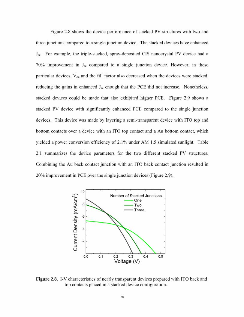
Figure 2.8 shows the device performance of stacked PV structures with two and
three junctions compared to a single junction device. The stacked devices have enhanced
Jsc. For example, the triple-stacked, spray-deposited CIS nanocrystal PV device had a
70% improvement in Jsc compared to a single junction device. However, in these
particular devices, Voc and the fill factor also decreased when the devices were stacked,
reducing the gains in enhanced Jsc enough that the PCE did not increase. Nonetheless,
stacked devices could be made that also exhibited higher PCE. Figure 2.9 shows a
stacked PV device with significantly enhanced PCE compared to the single junction
devices. This device was made by layering a semi-transparent device with ITO top and
bottom contacts over a device with an ITO top contact and a Au bottom contact, which
yielded a power conversion efficiency of 2.1% under AM 1.5 simulated sunlight. Table
2.1 summarizes the device parameters for the two different stacked PV structures.
Combining the Au back contact junction with an ITO back contact junction resulted in
20% improvement in PCE over the single junction devices (Figure 2.9).
Figure 2.8. I-V characteristics of nearly transparent devices prepared with ITO back and top contacts placed in a stacked device configuration.

29
Figure 2.9. I-V characteristics of two CIS nanocrystal PVs measured independently and in a stacked configuration under AM1.5 illumination.
Table 2.1. Summary of device characteristics obtained from stacked junction spray-deposited CIS nanocrystal devices with transparent back contacts.
The reason that all of the gains in Jsc have not translated directly into higher
device efficiency is that the ITO contacts have suffered from a relatively low shunt
resistance. Figure 2.10 shows a comparison of the dark I-V characteristics of CIS
nanocrystal devices prepared with Au and ITO back contacts. The series resistance (Rs)
Multiple Transparent Junctions Highest Efficiency Stacked Device
One Junction
Two Junctions
Three Junctions
Bottom Device
Top Device
Stacked Device
ηAM1.5 1.1% 1.11% 0.97% 1.79% 1.01% 2.10% Jsc (mA/cm2) 5.34 7.907 8.87 7.96 4.62 10.88 Voc (mV) 467 371 349 468 458 465 Fill Factor 0.442 0.379 0.349 0.479 0.478 0.414

30
and shunt resistance (Rsh) of the devices were estimated by fitting the data to a diode
equation,
10
0sh
snkT
IRV
ARJ
IRVeAJI
s
. (2.1)
A is the area, J0 is the saturation current density under reverse bias, and n is the ideality
factor of the device, with k and T representing Boltzmann’s constant and the temperature.
Devices made with Au back contacts have significantly higher shunt resistance than the
devices with ITO back contacts. Lower shunt resistance leads to reduced Voc and FF and
power conversion efficiency and must be improved in order to realize the full benefit of
stacking the semi-transparent PVs. The stacked device structure used in Figure 2.9 is an
example of a structure in which the use of lower performance ITO contacts is minimized
by using a Au bottom contact, which also provides a reflective back contact to help
increase the total amount of light absorption by the device.
Figure 2.10. I-V characteristics of typical diodes used for the stacked structure devices that were prepared on Au and ITO back contacts. Measured data (open circles) were modeled (solid lines) using Eqn (2.1). The best fit of Eqn (2.1) to the data gives the diode parameters tabulated in the inset.

31
2.4 Conclusions
PV devices with reproducible and reliable power output were fabricated by spray-
coating CIS nanocrystals without post-deposition annealing. Layered
Au/CIS/CdS/ZnO/ITO PV devices exhibited power conversion efficiencies of up to 1.9%
for single-junction devices and 2.1% for stacked-junction devices under AM 1.5
illumination. The device efficiency still requires significant improvement; however, it is
similar to that of other nanocrystal devices that have been fabricated without post-
deposition high temperature annealing. For example, Cd- and Pb-containing nanocrystal
devices have exhibited efficiencies as high as 3.6%,17-21 and Cu2S or Cu(Zn,Sn)S2
systems have demonstrated efficiencies up to 1.5%.22-24 Nanocrystal-based devices in
general have suffered to date from low Jsc. One approach to improving Jsc is to perform a
post-deposition high temperature anneal to sinter the films and reduce the grain boundary
density in the film, as Hillhouse and Agrawal have demonstrated for CuIn1-xGax(S1-ySey)2
PVs, in which they have achieved power conversion efficiency of more than 10%.13-14
Stacking single-junction nanocrystal devices provides a potential route for improved light
harvesting and increased Jsc for significantly improved power conversion efficiency
without the need for high temperature annealing.
A nanocrystal ink that could be used to fabricate high efficiency PVs without the
need for high temperature processing would change the way PVs are made. New contact
and substrate combinations could be used, with high throughput roll-to-roll processing on
lightweight, flexible plastic substrates. At the moment, however, nanocrystal-based PVs
require higher efficiency. This means that a better understanding of how to passivate
defects and traps in the nanocrystal layers and at materials interfaces in the devices,

32
without resorting to high temperature sintering, is needed and remains an ongoing topic
of research. Next chapter discusses the limitations of nanocrystal based devices and
provides a numerical measurements of the limitations in these devices.
2.5 Notes and References
1. Trends in Photovoltaic Applications, (International Energy Agency: Photovoltaic Power Systems Programme), 2009, http://www.iea.pvps.org/products/download/rep1_18.pdf.
2. S. H. Wei, A. Zunger, J. Appl. Phys.78 (1995) 3846–3856.
3. I. Repins, M.A. Contreras, B. Egaas, C. DeHart, J. Scharf, C.L. Perkins, B. To, R. Noufi, Prog. Photov: Res. Appl. 16 (2008) 235–239.
4. Companies reporting or given a timetable for production of commercial CIGS solar cells include Miasolé, Solyndra, HelioVolt, Nuvosun, Nanosolar, SoloPower, Ascent Solar and Solorion among others. Ascent Solar and Solorion are working on manufacturing flexible solar panels on metal foils. SulfurCell, Johanna Solar Technologies and Applied Quantum Technologies are working on manufacturing commercial CIS modules. Centrotherm Inc now offers full manufacturing line specifically focused on vapor deposited CIGS manufacturing.
5. M. Powalla, B. Dimmler, Thin Solid Films 361–362 (2000) 540–546.
6. R. Noufi, R. Axton, C. Herrington, S.K. Deb, Appl. Phys. Lett, 45 (1984) 668–670.
7. K.E. Knapp, T.L. Jester, G.B. Mihalik, Proceedings of 28th IEEE Photovoltaic Specialist Conference, Piscataway, 2000
8. J.R. Tuttle, T. Schuyler, E. Choi, J. Freer, Proceedings of the 20th European Photovoltaic Solar energy Conference and Exhibition, Barcelona, 2005
9. F. Kessler, D. Rudmann, Solar Energy 77 (2004) 685–695.
10. A.N. Tiwari, M. Krejci, F-J. Haug, H. Zogg, Prog. Photov.: Res. Appl. 7 (1999) 393–397.
11. M.G. Panthani, V. Akhavan, B. Goodfellow, J.P. Schmidtke, L. Dunn, A. Dodabalapur, P.F. Barbara, B.A. Korgel, J. Am. Chem. Soc.,130 (2008) 16770–16777.

33
12. Q. Guo, S.J. Kim, M. Kar, W.N. Shafarman, R.W. Birkmire, E.A. Stach, R. Agrawal, H.W. Hillhouse, Nano Lett. 8 (2008) 2982–2987.
13. Q. Guo, G.M. Ford, H.W. Hillhouse, R. Agrawal, Nano Lett. 9 (2009) 3060–3065.
14. Q. Guo, H.W. Hillhouse and R. Agrawal, 2009 AIChE Annual Meeting, Nashville, 2009, 447C.
15. B. E. McCandless and W. N. Shafarman, U.S. Patent 6,537,845, 2003.
16. U. Rau, H.W. Schock, Appl. Phys. A 69 (1999) 131–147.
17. I. Gur, N.A. Fromer, M.L. Geier, A.P. Alivisatos, Science 310 (2005) 462–465.
18. J.M. Luther, M. Law, M.C. Beard, Q. Song, M.O. Reese, R.J. Ellingson, A.J. Nozik, Nano Lett. 8 (2008) 3488–3492.
19. W. Ma, J.M. Luther, H. Zheng, Y. Wu and A.P. Alivisatos, Nano Lett. 9 (2009) 1699–1703.
20. G.I. Koleilat, L. Levina, H. Shukla, S.H. Myrskog, S. Hinds, A.G. Pattantyus-Abraham, E. H. Sargent, ACS Nano 2 (2008) 833–840.
21. J.J. Choi, Y.F. Lim, M.B. Santiago-Berrios, M. Oh, B.R. Hyun, L. Sun, A.C. Bartnik, A. Goedhart, G.G. Malliaras, H.D. Abruna, F.W. Wise, T. Hanrath, Nano Lett. 9 (2009) 3749–3755.
22. Y. Wu, C. Wadia, W. Ma, B. Sadtler, A.P. Alivisatos, Nano Lett. 8 (2008) 2551–2555.
23. C. Steinhagen, M.G. Panthani, V. Akhavan, B. Goodfellow, B. Koo, B.A. Korgel, J. Am. Chem. Soc. 131 (2009) 12554–12555.
24. Q. Guo, H.W. Hillhouse, R. Agrawal, J. Am. Chem. Soc. 131 (2009) 11672–11673.

34
Chapter 3: Thickness-Limited Performance of CuInSe2 Nanocrystal Photovoltaic Devices*
3.1 Introduction
Various new approaches are being examined to produce “third generation”
photovoltaic devices (PVs) with very low cost and high efficiency.1-3 There is interest in
enhancing performance using nanostructured materials via new physical effects, such as
multi-exciton generation (MEG)4 and intermediate band absorption,5 as well as lowering
manufacturing costs by using new materials that can be deposited without the need for
high temperature and vacuum processing.6 Photovoltaics made of organics (OPVs) are
printable, do not require high temperature processing, and have demonstrated efficiencies
of 7.4% for solution processed devices.7 However, the most efficient devices have so far
required relatively expensive specialty chemicals to achieve high efficiencies.
Furthermore, achieving adequate photostability remains a major challenge with these
materials. An alternative to organic materials, which can still be printed and require only
moderate processing conditions, are dispersions, or inks, of inorganic nanocrystals. With
this approach, inorganic materials with proven and stable performance can be deposited
using by mild deposition processes typically only suitable for organic materials and not
crystalline semiconductors.8 Cd and Pb based nanocrystal PV devices9-13 have exhibited
power conversion efficiencies as high as 5.1%.14 However, the use of Cd and Pb is not
* Large portions of this chapter were reproduced with permission from: V. A. Akhavan, M. G. Panthani, B. W. Goodfellow, D. K. Reid and B. A. Korgel, “Thickness-Limited Performance of CuInSe2 Nanocrystal Photovoltaic Devices,” Energy Express, 18(S3), A411–A420 (2010). Copyright 2010 Optical Society of America.

35
very desirable from an environmental perspective due to their toxicity. Other more
environmentally-friendly semiconductor nanocrystals, such as Cu(In1-xGax)Se2,15
Cu2ZnSnS4 16-17 or Cu2S
18 have also been used to fabricate PVs, but with slightly more
moderate efficiencies of up to 1.6% to date. These multicomponent semiconductors are
difficult and expensive to prepare through conventional vapor deposition techniques.
Nanocrystal solution processing provides an inexpensive and simple processing route that
could be scaled to larger production lines and transferred to flexible and light-weight
plastic substrates. For commercialization, the device efficiency must be improved by
about a factor of 5 to 8.
The factors that limit nanocrystal-based PV device efficiency are still relatively
unexplored and to date, the highest efficiency nanocrystal PVs have been made by time-
consuming empirical optimization. The devices consist of several layers of different
materials and the quality of each layer and the interfaces critically impact the
performance of the devices. Here, we examine the factors related to the nanocrystal layer
and the semiconductor heterojunction that limit the efficiency of CuInSe2 nanocrystal-
based PVs.
Previous chapter demonstrated CuInSe2 nocrystal synthesis and the
implementation of CuInSe2 nanocrystals into functioning PVs.15 This chapter
demonstrates CuInSe2 nanocrystal device efficiency reaching 3.1% without the need for
high temperature annealing. We report these results here, and examine the factors that
are limiting device efficiency.

36
3.2. Experimental
3.2.1 Nanocrystal inks
CuInSe2 nanocrystals were synthesized by arrested precipitation using a
modification of previously reported procedures.15 Oleylamine (OLA; >70%),
tributylphosphine (TBP; 97%), copper(I) chloride (CuCl; 99.995%), indium(III) chloride
(InCl3; anhydrous 99.99%) and selenium (Se; 99.99%) were purchased from Aldrich
Chemical Co. and used as received.
5 mmol of CuCl, 5 mmol of InCl3 was combined with 50 ml of OLA in a three
neck flask in a nitrogen-filled glovebox. The flask was sealed by a condenser-stop cock
setup and two septa; the flask was brought outside and mounted on a Schlenk line. The
reaction mixture was heated up to 110 °C, degassed for 10 minutes by pulling vacuum on
the vessel and was purged with clean nitrogen for 5 minutes. While maintaining the
nitrogen environment, the reaction vessel was heated to 180 °C and 10 ml solution of 1 M
Se in TBP (0.79 g Se powder and 10 ml TBP) was injected into the reaction vessel. The
reaction mixture temperature was raised to 240 °C as quickly as possible and the reaction
was allowed to proceed for 10 minutes. The heating mantle was removed and the
reaction was cooled slowly to room temperature.
After cooling, the reaction mixture was transferred to a glass centrifuge tube. 10
ml of ethanol was added to the centrifuge tube, and the mixture was centrifuged at 4500
RPM for 10 minutes. The supernatant was discarded, and the solid precipitate was
dissolved in 10 ml of toluene. The new solution was centrifuged at 4500 RPM for 10
minutes to remove larger and poorly capped nanocrystals. The supernatant was
transferred to a new glass centrifuge tube, and the solid precipitate discarded. Ethanol

37
was added drop-wise to the particle solution until a turbid mixture was achieved. The
reaction was centrifuged again at 4500 RPM for 10 minutes. The supernatant was
discarded, and the precipitate dissolved in toluene to achieve a 20 mg/ml solution.
3.2.2 Materials characterization
TEM was performed on a Phillips 208 operated at 80 kV accelerating voltage or a
JEOL 2010F TEM at 200 kV accelerating voltage. TEM samples were prepared on a 200
mesh nickel grid (Electron Microscopy Sciences) by dropcasting a dilute solution of
nanocrystals in chloroform. EDS was carried out using an Oxford INCA EDS detector
mounted on the JEOL TEM or a Bruker Quantax 200 detector mounted on a Hitachi S-
5500 STEM. SEM images were collected using a Zeiss Supra 40 VP SEM operated at 10
kV accelerating voltage. Images were collected through the in-lens detector. SEM
samples were prepared by depositing a thin layer of the nanocrystals on a conductive
surface. XRD data was collected on a Bruker-Nonius D8 advance θ−2θ powder
diffractometer equipped with a Bruker Sol-X Si(Li) solid state detector and a rotating
stage. 1.54 Å radiation (Cu Kα) was used to collect at 0.02 increments of 2θ at a scan rate
of 12 °/min while the sample was rotating at 15 RPM. XRD samples were prepared by
depositing a relatively thick (≈ 10 μm) film of nanocrystals on a glass substrate. UV-vis-
NIR absorbance spectra were measured using a Varian Cary 500 spectrophotometer.
3.2.3 PV device fabrication
PV devices were fabricated with a layered CuInSe2/CdS/i-ZnO structure, similar
to reported by Contraras [19]. Sodalime glass substrates (Delta Techology) were cleaned
by sonication in an acetone/isoproponol mixture, followed by rinse with DI water, and
drying under nitrogen. Back contact layers of 5 nm thick Cr (99.999%, Lesker) adhesion

38
layer with 60 nm of Au (99.95%, Lesker) were deposited by thermal evaporation.
Nanocrystal dispersions were deposited on the Au back contacts by spray deposition of
dispersions in toluene with concentrations of 20 mg/ml nanocrystals using a commercial
spray gun (Iwata Eclipse HP-CS) operated at 50 psig head pressure. The nanocrystal
layer was obtained by profilometry or from SEM images of cross-sectioned devices.
Following nanocrystal deposition, CdS layer was deposited with the method reported by
McCandless and Shafarman [20]. Then, 50 nm of ZnO was AC sputtered (99.9% Lesker,
5 ppm O2 in Ar sputtering gas) followed by another 600 nm layer of sputtered ITO
(99.99% Lesker, UHP Ar sputtering gas). The final active area of the device is 8 mm2, a
4 mm by 2 mm rectangle. Completed devices were placed in a vacuum oven at 200 °C
for up to 40 minutes to improve the device performance.
Mott-Schottky measurements were performed on PVs with slightly different
structures. 300 nm of AC sputtered ITO was used as substrate to deposit CuInSe2
nanocrystal films as described above. Top contact was a 40 nm layer of Al (Lesker,
99.99%) thermally evaporated from a tungsten boat. The active device area was 8 mm2.
3.2.4 PV device testing
Current-potential (I-V) characteristics were collected using a Keithley 2400
general purpose sourcemeter and a Xenon lamp solar simulator (Newport) equipped with
an AM1.5 optical filter. Intensity of the light source was calibrated using a NIST
calibrated Si photodiode (Hamamatsu, S1787-08). Different fractions of solar spectrum
were generated by placing a colored glass, cutoff filters (Newport) directly in the path of
light beam emanating from the solar simulator. Incident photon-to-electron conversion
efficiency (IPCE) measurements were performed at zero bias between 300 and 1100 nm

39
in 10 nm steps using an in-house fabricated spectrophotometer. Monochromatic light
was generated using a commercial monochromator (Newport Cornerstone 260 1/4M).
Generated light was chopped at 213 Hz and was focused to a spot size of 1 mm in
diameter on the active region. The response of the device was recorded using a lock-in-
amplifier (Stanford Research Systems, model SR830). The light intensity was calibrated
using calibrated photodiodes of silicon (Hamamatsu) and germanium (Judson).
Impedance characteristics was measured by applying a 50 mV A-C waveform at
frequencies between 0.1 Hz and 107 Hz with 5 steps per decade, using a Solartron 1260A
Frequency Response Analyzer coupled with a Solartron 1296 Dielectric Interface.
3.3 Results and Discussion
3.3.1 CuInSe2 nanocrystal inks
Figure 3.1 shows TEM images and XRD data for the CuInSe2 nanocrystals used
to fabricate the PV devices. The nanocrystals are crystalline, with irregular, faceted
shape and an average diameter of 14 nm ± 4 nm. XRD (Figure 3.1C) and EDS confirmed
that the nanocrystals have chalcopyrite crystal structure with stoichiometric (1:1:2)
Cu:In:Se composition. Figure 3.1 also shows an illustration of the chalcopyrite unit cell
of CuInSe2. The nanocrystals are coated with a monolayer of oleylamine, which
stabilizes their size and provides dispersibility in organic solvents.

40
Figure 3.1. (A, B) TEM images and (C) XRD of the CuInSe2 nanocrystals. The diffraction peaks in (C) are indexed to chalcopyrite CuInSe2 (PDF#97-006-8928). The inset shows the chalcopyrite unit cell of CuInSe2: red, blue and green spheres correspond to copper, indium and selenium atoms, respectively.
3.3.2 PV device fabrication
PV devices were fabricated by spray-coating the CuInSe2 nanocrystal ink onto Au
back contacts on glass substrates. Nanocrystal films with uniform thickness with few
pinholes or cracks are obtained using this method. Devices have been made using this
approach with power conversion efficiencies under AM1.5 illumination of up to 3.1%.
Figure 3.2 shows the dark and light I-V curves for the device with highest power
conversion efficiency (PCE).

41
Figure 3.2. I-V characteristics of a device with power conversion efficiency of 3.1% under AM1.5 illumination. Dark conditions (black) and under AM1.5 irradiation (red). The device parameters are obtained by a best fit of Eqn (3.1) (solid lines) to the data (). The parameters from the best fit are listed in table 3.1.
3.3.3 Diode behavior in the dark and light
The device in Figure 3.2 exhibits a “crossover” between the dark and the light I-V
curves at forward bias, which is commonly observed in our devices. This crossover is
undesirable as it leads to a decrease in device efficiency, and ideally should be prevented.
The reason for this crossover can be deduced by modeling the device current density, J,
based on a single junction diode model:
00
1sV JAR
snkTph
sh
V JARJ J e J
J AR
(3.1)
In Eqn (3.1), J0 is the reverse bias saturation current density, A is the device area,
n is the ideality factor of the diode, Rs is the series resistance of the diode, Rsh is the shunt
resistance of the diode, Jph is the photogenerated current density, k is Boltzmann’s
constant and T is temperature. Table 3.1 lists the device parameters obtained by fitting
Eqn (3.1) to the device data in Figure 3.2. The large value of n, greater than 3, suggests
that the devices are dominated by recombination current and illumination with light

42
increases the non-ideality of the diode. Rs and Rsh both decrease under illumination and
J0 increases by two orders of magnitude, indicating that the crossover is an outcome of
photoconductivity of the materials in the device—mostly likely the CdS layer (see
discussion in next paragraph). A reduction in Rs is desirable, as it lowers the barrier for
current extraction, but reduced Rsh and increased J0 are undesirable and result from
higher recombination within the device.
Table 3.1. Diode performance parameters for the highest efficiency PVs.
Dark AM1.5 illumination J0 (μA/cm2) 3.2 200 n 3.1 3.8 Rs (Ω) 57 29 Rsh (kΩ) 1300 2.0 Jph (mA/cm2) --- 16.5
The origin of the photoconductivity effect leading to the crossover of the light and
dark curves in the devices discussed above was examined by shining light on the device
with different ranges of wavelengths. The CuInSe2 nanocrystals have a band gap of
about 1 eV, corresponding to a wavelength of 1236 nm. ZnO and CdS have much wider
band gaps of 3.3 eV and 2.4 eV, corresponding to wavelengths of 375 nm and 515 nm,
respectively. Figure 3.3A shows the I-V response of the device when it was illuminated
with light with the high energy photons filtered out, as shown in Figure 3.3B.

43
Figure 3.3. (A) I-V measurements of a CuInSe2 nanocrystal PV device with a crossover between the light and the dark curves. Using light with wavelength higher than 515 nm, the crossover is still present. By using only low energy photons above 630 nm wavelength, however, the cross over between the dark and light curves is eliminated. (B) Spectra of light used for each illuminated measurement.
As shown in Figure 3.3A, the amount of crossover between the light and dark
curves decreased when the shorter wavelength light was filtered, and it was completely
eliminated when the illumination had wavelengths larger than the absorption edge of the
CdS (515 nm) layer. Similarly, the shunt current in the reverse bias is reduced as longer
wavelength light is used. These data show that it is the CdS buffer layer that leads to the
high leakage current under illumination. .
Elimination of the shorter wavelength light and higher series resistance also
significantly changed the fill factor of the device. The devices performed well under
AM1.5 illumination, with a fill factor of 0.56. With a 515 nm cutoff filter, the fill factor
decreased to 0.29, and with a 630 nm cutoff filter, it decreased to 0.24. Low fill factors
in vapor-deposited CuInSe2 21 have been attributed to type-I band alignment between the
CuInSe2 and CdS layers. Scheme 3.1 shows the expected band alignment at the
CuInSe2/CdS/ZnO heterojunction.22 The CuInSe2 nanocrystals are p-type, and there is

44
expected to be a “spike” in the conduction band alignment with the CdS buffer layer that
creates a barrier to electron extraction under forward bias. The CdS buffer layer has a
significant concentration of low energy donors that lead to its n-type behavior. There are
additional deep electron traps, however, that reduce the concentration of mobile carriers
present in the n-type CdS layer. When excitons are generated in the CdS layer, the deep
traps are compensated by “photo-doping”,23 which increases the number of mobile
carriers, reduces the barrier to electron transport across the CdS layer and leads to an
increased junction conductance (Scheme 3.1).21,24 Increased conductance is the reason
for the observed crossover of the dark and light I-V curves. Additionally, as the
concentration of mobile carriers in the CdS layer is increased, the Schottky barrier
between the n-type CdS layer and the Au back contact is reduced, that can lead to higher
leakage current through pinholes and cracks in the nanocrystal film when illuminated.
Scheme 3.1. Band alignment of CuInSe2/CdS/ZnO heterojunction with or without the photo-doping of the CdS buffer layer. Modified from Poduv, et. al. [2]
3.3.4 Device performance limitation
Device efficiencies of 3% are too low for commercialization and need to be
improved.25 The highest efficiency devices are actually composed of relatively thin

45
nanocrystal layers that are only about 150 nm thick. We have found that increasing the
nanocrystal layer thickness enhances light absorption but it does not improve device
efficiency. Figure 3.4 shows I-V characteristics of devices made with nanocrystal films
of increasing thickness. Jsc actually decreased when the nanocrystal films were made
thicker, even though more electrons and holes are being photogenerated. This indicates
that the photogenerated carriers cannot be extracted from the nanocrystal layer unless
they are relatively close to the junctions.
Figure 3.4. (A) I-V measurements of devices with varying thickness of spray deposited CuInSe2 nanocrystal film and (B) calculated device parameters associated with these devices.
Measurements of the incident photon-to-electron conversion efficiency (IPCE)
provide additional insight into how well the devices are performing and what the limiting
factors are. In IPCE measurements, the short circuit current is measured as a function of
the wavelength of the incident illumination. Figure 3.5A shows IPCE measurements for
devices with varying nanocrystal layer thickness. The IPCE data is essentially an
external quantum efficiency (at zero bias) that does not account for how much light is
absorbed by the device—it is a measure of charge carriers extracted based on the number
of photons that are illuminating the device. Another useful quantity is the internal

46
quantum efficiency, which provides an accounting of the photon absorption and tells
what fraction of the photogenerated carriers are actually extracted from the device.
Figure 3.5. (A) IPCE measurements of a set of devices with different thicknesses of the CuInSe2 nanocrystal film thickness shows similar trend between the different thicknesses. (B) Internal quantum efficiency data of the same devices reveals how thinner devices extract photogenerated carriers at a better efficiency.
The internal quantum efficiency of the devices, IQE(λ), is the ratio of the
wavelength-dependent IPCE, IPCE(λ), to the fraction of the incident light at that
wavelength that is absorbed by the CuInSe2 nanocrystal films, f(λ). f(λ) is determined
from the transmittance of the top window layer, Ttop(λ); the transmittance of the CuInSe2
nanocrystals layer, T1(λ); and the reflectivity of the back contact, RBC(λ).
2
11top BCf T T R (3.2)
It should be noted that this estimate of the IQE(λ) does not account for internal
reflection or optical interference effects that may also contribute to f(λ) and represents an
upper bound. Figure 3.5B shows the device IQE(%) for devices with different
nanocrystal layer thickness. Consistent with the reduced Jsc for devices with thicker
nanocrystal films, the thinner devices have much higher IQE, indicating that they are

47
much better at extracting photogenerated carriers, across a side range of wavelength, than
the thicker devices.
The higher IQE and more efficient device performance of the thinner devices is
also enhanced by light reflection from the back contact. Especially, the thinner films
benefit from a “second pass” of light reflected off the back contact. This is evident in the
IPCE measurements at longer wavelegths (600 nm to 1200 nm) where only a very small
fraction of the incident light is absorbed by the thinner layers on the first pass. As the
films get thicker, a large fraction of the incident photons are absorbed deeper in the
nanocrystals layer and the resulting photogenerated carriers are unable to be efficiently
extracted. This data also indicates that the photogenerated carriers can only be extracted
efficiently when they are generated close to the CuInSe2/CdS/ZnO heterojunction.
3.3.5 Impedance spectroscopy
The thickness of the active region in the nanocrystal layer in the device was
determined by measuring the impedance of the devices. Figure 3.6C shows typical
impedance data on a CuInSe2 nanocrystal PV device with slightly modified structure.
The device geometry (shown in Figure 3.6A) was devised to ensure that carrier depletion
was limited to the spray deposited CuInSe2 film. The circuit model shown in Figure 3.6B
was found to provide the best fit to the impedance data. The capacitance of the space
charge region Csc, was extracted to determine the majority carrier density and an effective
depletion width in the nanocrystal layer using a Mott-Schottky analysis. Csc is related to
the doping level NA, and applied voltage V:
2 20
1 2bi
sc A s
kTV V
qC qN A
(3.3)

48
In Eqn (3.3), Vbi is the built-in voltage of the junction, q is the elementary charge
of an electron, ε0 is the vacuum permittivity and εs is the relative permittivity of CuInSe2
(≈ 10). Figure 3.6D shows Csc-2 plotted against V. Values of NA and Vbi were determined
by fitting Eqn (3.3) to the data. The depletion layer width can be estimated from the
relation:
2 2
02bi A p D ns
qV N x N x
(3.4)
NA and ND are acceptor and donor concentrations in the p-type and n-type layers,
respectively, and xp and xn are the depletion layer widths of the p-type and n-type layers,
respectively. With the device design shown in Figure 3.6A, depletion occurs only in the
p-type nanocrystal layer, and Eqn (3.4) simplifies to
2
02A p
bis
qN xV
(3.5)
In a typical device the depletion region thickness was found to be 55 nm in the
dark. When the device was illuminated, the depletion region thickness was found to
decrease to 45 nm (under AM1.5 illumination). The change in doping level in the CdS
layer under light leads to a noticeable change in the device properties, as discussed above.
Further work is underway to gain a more detailed understand about the band alignment
between layers in the nanocrystal devices.

49
Figure 3.6. (A) Device architecture used for C-V measurements consists of a simplified junction. (B) One diode model considered for this type of junction to analyze the impedance data. (C) Sample Nyquist plot illustrating the response of the junction at a certain bias; inset provides the parameters gathered from the model fit (solid line) for the equivalent circuit to the raw data (marked by ). (D) Linear plot of inverse square capacitance of the junction versus applied voltage across the junction, inset provides the gathered parameters based on Mott-Schottky approximation. Area of this device was isolated to 8 mm2. (E) I-V characteristics of this junction show that it shows a very similar response to the more complex conventional devices, inset lists the device parameters.
3.4 Conclusion
Power conversion efficiencies above 3% under AM1.5 are demonstrated for ambient
processed CuInSe2 nanocrystal-based PVs. The extraction of photogenerated carriers
from deep within the CuInSe2 nanocrystal film remains a major challenge. The high

50
concentration of crystal interfaces leads to high recombination. A Mott-Schottky analysis
of the space-charge capacitance in the device revealed that the active region of the device
is only about 50 nm thick, which is consistent with IPCE and IQE measurements on
devices with varying nanocrystal film thickness. Future efforts must focus on increasing
the thickness of the space charge region to extract carriers deeper in the nanocrystal layer
in order to improve device efficiency. Next chapter overviews the attempts to increase
the Jsc of nanocrystal based devices through increasing the space charge region in the
nanocrystal films. Synthetic procedures or chemical treatment routes were investigated to
avoid high temperature selenization of the films.
3.5 Notes and References
1. M. Grätzel, Phil. Trans. R. Soc. A 365 (2007) 993–1005.
2. R. Po, M. Maggini, N. Camaioni, J. Phys. Chem C 114 (2010) 695–706
3. L.L. Kazmerski, J. Electron Spectroscopy and Related Phenomena 150 (2006) 105–135.
4. P.T. Landsberg, H. Nussbaumer, G Willeke, J. Appl. Phys. 74 (1993) 1451–1452.
5. A. Luque, A. Marti, Phys. Rev. Lett. 78 (1997) 5014–5017.
6. K.E. Knapp, T.L. Jester, Proc. of 28th IEEE Photovoltaic Specialist Conf, Piscataway (2000).
7. Y. Liang, Z. Xu, J. Xia, S-T. Tsai, Y. Wu, G. Li, C. Ray, L. Yu, Adv. Mater. 22 (2010) E135–E138.
8. A. J. Nozik, Physica E 14 (2002) 115–120.
9. I. Gur, N.A. Fromer, M.L. Geier, A.P. Alivisatos, Science 310 (2005) 462–465.
10. J.M. Luther, M. Law, M.C. Beard, Q. Song, M.O. Reese, R.J. Ellingson, A.J. Nozik, Nano Lett. 8 (2008) 3488–3492.
11. W. Ma, J.M. Luther, H. Zheng, Y. Wu, A.P. Alivisatos, Nano Lett. 9 (2009) 1699–1703.

51
12. G.I. Koleilat, L. Levina, H. Shukla, S.H. Myrskog, S. Hinds, A.G. Pattantyus-Abraham, E.H. Sargent, ACS Nano 2 (2008) 833–840.
13. J.J. Choi, Y.F. Lim, M.B. Santiago-Berrios, M. Oh, B.R. Hyun, L. Sun, A.C. Bartnik, A. Goedhart, G.G. Malliaras, H.D. Abruna, F.W. Wise, T. Hanrath, Nano Lett, 9 (2009), 3749–3755.
14. A.G. Pattantyus-Abraham, I.J. Kramer, A.R. Barkhouse, X. Wang, G. Konstantatos, R. Debnath, L. Levina, I. Raabe, M.K. Nazeeruddin, M. Gratzel, E.H. Sargent, ACS Nano 4 (2010) 3374–3380.
15. M.G. Panthani, V. Akhavan, B. Goodfellow, J.P. Schmidtke, L. Dunn, A. Dodabalapur, P.F. Barbara, B.A. Korgel, J. Am. Chem. Soc. 130 (2008) 16770–16777.
16. C. Steinhagen, M.G. Panthani, V. Akhavan, B. Goodfellow, B. Koo, B.A. Korgel, J. Am. Chem. Soc. 131 (2009) 12554–12555.
17. Q. Guo, H.W. Hillhouse, R. Agrawal, J. Am. Chem. Soc. 131 (2009) 11672–11673.
18. Y. Wu, C. Wadia, W. Ma, B. Sadtler and A.P. Alivisatos, Nano Lett. 8 (2008) 2551–2555.
19. L. Stolt, J. Hedström, J. Kessler, M. Ruckh, K-O. Velthaus and H-W. Schock, Phys. Lett. 62 (1993) 597–599.
20. B.E. McCandless, W.N. Shafarman, U.S. Patent 6,537,845 (2003)
21. A.O. Pudov, J.R. Sites, M.A. Contreras, T. Nakada, H-W. Schock, Thin Solid Films 480–481 (2005) 273–278.
22. U. Rau, H-W. Schock, Appl. Phys. A 69 (1999) 131–147.
23. A. Niemegeers, M. Burgelman, A. De Vos, Appl. Phys. Lett. 67 (1995) 843–845.
24. M. Burgelman, F. Engelhardt, J.F. Guillemoles, R. Herberholz, M. Igalson, R. Klenk, M. Lampert, T. Meyer, V. Nadenau, A. Niemegeers, J. Parisi, U. Rau, H–W. Schock, M. Schmitt, O. Seifert, T. Walter, S. Zott, Prog. Photov: Res. Appl. 5 (1997) 121–130.
25. V.A. Akhavan, B.W. Goodfellow, M.G. Panthani, B.A. Korgel, Modern Energy Review 2 (2010) 19–21.

Chapter 4: Improved Device Performance with Modification to Synthetic Chemistry and Low-Temperature
Treatment of Nanocrystal Inks
4.1 Introduction
Using nanocrystals for electronic applications requires uninhibited movement of
charge carriers through the nanocrystal layer. High density conduction is particularly
important in operation of photovoltaic (PV) devices. As was discussed in Chapters 2 and
3, limited carrier diffusion length combined with high recombination current significantly
hinder the potential for extracted current densities.
Mechanism for carrier drift and diffusion through the nanocrystal layers underline
the challenges of charge collection. Individual nanocrystals are typically synthesized and
dispersed with a layer of surfactant surrounding the crystalline core. Once deposited, the
resulting films are heterogeneous in composition with large concentration of interfaces.
Even though, movement of carriers within the crystalline grain is dominated by highly
effective solid state physics, the hopping between distinct nanocrystal grains limits the
carrier mobility in as-deposited nanocrystal films. Presence of the electronically
insulating organic surfactant on the surface prevents crystalline cores from contacting and
requires carrier tunneling for charge to move between individual nanocrystals. The
conduction of carriers in nanocrystalline films have been well documented in the Pb and
Cd chalcogenide based quantum dots.1-10
As-deposited nanocrystal films exhibit strong Coulomb blockade at room
temperature which results in reduced carrier mobilities.1 Coulomb blockade can be
mitigated with increased conduction through the film. Chemical or thermal treatment of
52

the as-deposited nanocrystal layer can remove a large fraction of the original ligand. Use
of shorter, bi-functionalized, capping ligands (such as ethanedithiol,11-12 hydrazine13-14 or
benzenedithiol15-17) can replace the synthesis ligand (which is typically much longer) on
the surface, reduce interparticle spacing of crystalline grains and increase the charge
mobility in the nanocrystalline film. Higher conduction eliminates buildup charge due to
Coulomb blockade in the treated films.5 Stronger electronic coupling between
nanocrystal grains can produce bulk semiconductors like conduction regimes.
As synthesized CIGS nanocrystalline grains have an average diameter of 15 nm.
The crystal domains are too large to experience Coulomb blockade like the smaller Cd
and Pb based quantum dots. The insulating nature of the capping ligand (oleylamine)
used, however, can lead to build up and trapping of charge within the nanocrystalline
films. Even so, 3% PCE devices could be fabricated from as-deposited nanocrystals.18
The ability of chemical or thermal treatment to improve conduction through the film was
investigated to improve device performance. Increased conduction, however, did not
translate into increased device efficiency. Chemical and thermal treatments were found
to be detrimental to photovoltaic efficiencies of nanocrystal devices. The loss of
efficiency is attributed to the increased defect states on the surface of nanocrystal grains
with the treatment of the nanocrystal films. Higher recombination limits the benefits of
higher mobility.
To prevent formation of defects in the nanocrystalline films, thermal treatments of
the completed devices were performed. Once the devices are complete, the nanocrystal
layer has limited access to the ambient atmosphere, reducing the kinetics of defect
formation. It was discovered that a 3 improvement in the Jsc and a 2 improvement in
53

the overall efficiency of the devices can be achieved thorugh post completion treatment
of the devices. Impedance spectroscopies of the treated diodes indicate a reduction in the
series resistance of the device with thermal treatment. Lower resistive barrier to charge
extraction results in higher efficiency devices.
Impact of size, shape and composition of the nanocrystalline grains on the device
performance were also investigated. Depositing larger nanocrystals with shorter ligands
would significantly increase carrier mobility in the nanocrystal films. Work of Matthew
Panthani has demonstrate, synthetic control over the nanocrystal product is difficult.
Here we demonstrate three differently shaped nanocrystals with different overall
compositions. To study improvements in device efficiency through composition and
shape control requires independent synthetic control over each variable. This
understanding is still lacking for the CIGS based nanocrystals. It was, however,
discovered significant differences exist between different synthetic routes and
precurssors. “Hot-injection” synthetic route produced consistently higher efficiency
devices. While the improvements in efficiency are relatively small, this research
highlights the need to better understand the shape and composition of nanocrystal grains
for device fabrication.
4.2 Experimental Details
4.2.1 Materials
Oleylamine (OLA) was purchased from Fisher Chemical Co. (Acros brand), and
TCI America; copper (I) chloride (CuCl; 99.99+%), selenium powder (Se; 99.99%),
tributylphosphine (TBP, 95%), and cadmium sulfate (CdSO4; 99.999%) from Aldrich
54

Chemical Co.; indium (III) chloride (InCl3; 99.999%) from Strem Chemicals; ammonium
hydroxide (18M NH3; ACS certified), toluene (99.99%), nitric acid (trace metal grade),
and ethanol (absolute) from Fischer Scientificy; and thiourea (> 99%) from Sigma-
Aldrich. Oleylamine was degassed overnight by pulling vacuum on OLA heated to
110oC. All other chemicals were used as received without further purification. Copper
(I) chloride, indium (III) chloride, and degassed oleylamine were stored in a nitrogen-
filled glovebox to prevent degradation.
4.2.2 CuInSe2 nanocrystal syntheses
Two different synthetic routes were examined to create nanocrystal inks. First
route involved one pot synthesis of nanocrystals using elemental selenium and the second
route involved direct injection of tributylphosphine (TBP) and Se complex at elevated
temperatures.
A typical one-pot reaction was carried out by combining, in a three neck flask, 5
mmol of CuCl, 5 mmol of InCl3, 10 mmol of Se, and 50 ml of degassed oleylamine
inside a nitrogen-filled glovebox. The flask necks were sealed with septa before
removing the flask from the glovebox and attaching it to a Schlenk line equipped with a
stirring plate and a heating mantle. The reaction mixture was stirred continuously and
heated to 110°C to degas for 30 minutes by pulling vacuum. It is then purged and held
under a nitrogen environment. The vessel was heated to 200°C for 30 minutes to dissolve
all the constituent solids. The reaction mixture was then heated to 260°C and the reaction
proceeds for an additional 10 minutes. The heating mantle is then removed and the
reaction is slowly cooled to room temperature. After cooling, the flask is removed from
55

the Schlenk line and the reaction product is poured into glass centrifuge tubes for
cleaning.
A typical hot-injection reaction was carried out in a similar three neck flask. In
this case, 5 mmol of CuCl, 5 mmol of InCl3, and 50 ml of degassed oleylamine (no
selenium) were loaded into the flask inside a nitrogen-filled glovebox. All the necks
were sealed with septa before removing from the flask from the glovebox and loading
onto the Schlenk line. The reaction vessel was similarly degassed at 110°C for 30
minutes and refilled with dry nitrogen. While maintaining the nitrogen environment, the
vessel was heated to 180°C for 5 minutes to dissolve all the solid precursors. A 10 ml
solution of 1M Se in TBP (0.79g Se powder in 10 ml of TBP) was then injected through
one of the septa capped necks into the reaction vessel, the reaction temperature as raised
to 240°C as quickly as possible and held there for 10 minutes to complete the reaction.
The heating mantle was then removed and the reaction is slowly cooled to room
temperature. The content of the reaction vessel was then emptied into glass centrifuge
tubes.
Both synthesis products were cleaned in identical manner. The nanocrystals were
precipitated with excess ethanol and centrifugation at 4000 rpm for 2 min. After
centrifugation, the supernatant was discarded and the precipitate was redispersed using a
minimal amount of toluene, usually 5 ml as it depends on the yield of the reaction. The
solution was then centrifuged at 4000 rpm for 1 min to remove large and poorly-capped
nanocrystals. The supernatant was then transferred to a clean glass centrifuge tube and
the precipitate was discarded. Ethanol was then added dropwise to the nanocrystals
solution until the mixture becomes slightly turbid. The mixture was centrifuged at 4000
56

rpm for 1 min, after which the supernatant was discarded. The precipitate dissolved in a
small amount of toluene to form 20 mg/ml suspension and was sprayed after synthesis to
form active devices.
4.2.3 PV device fabrication
Sodalime glass substrates (Delta Technology) were cleaned by sonication in an
acetone/isoproponol mixture, followed by rinse with DI water, and drying under nitrogen.
Back contact layers containing 60 nm Au (99.95% Lesker) and 5 nm Cr (99.999%
Lesker) strike layer were thermally evaporated using a Denton evaporation system. The
final sheet resistance of the combined back contact structure was ~ 3 Ω/.
Nanocrystal dispersions were deposited on the back contacts by spray deposition
of 20 mg/ml dispersion of nanocrystals in toluene using a commercial spray gun (Iwata
Eclipse HP-CS) operated at 50 psig head pressure. Films were sprayed in one step to a
targeted thickness close to 200 nm. A thin CdS layer was deposited on the nanocrystal
layers immediately after spray deposition. To fabricated photovoltaic devices, the CdS
deposition was followed by 50 nm of AC sputtered ZnO (99.9% Lesker, 5 ppm O2 in Ar
sputtering gas) and 600 nm layer of sputtered ITO (99.99% Lesker, UHP Ar sputtering
gas) to complete a transparent top electrode. With the final active area of the device is 8
mm2, a 4 mm by 2 mm rectangle. To make the devices used for Mott-Schottky analysis,
50 nm of AC sputtered ZnO was followed by 50 nm of thermally evaporated Al (99.99%
Lesker). The area of the devices were similar at 8 mm2.
57

4.2.4 Characterization
Current-potential (IV) characteristics were collected using a Keithley 2400 general
purpose source meter and a Xenon lamp solar simulator (Newport) equipped with an
AM1.5 optical filter. Intensity of the light source was calibrated using a NIST calibrated
Si photodiode (Hamamatsu, S1787-08).
Impedance characteristics of the photovoltaic cell were collected using a Solartron
1260A Frequency Response Analyzer coupled with a Solartron 1296 Dielectric Interface.
Measurements were taken between 0.1 Hz and 107 Hz with 5 steps per decade by
applying a 50 mV A-C waveform.
ICP-ms measurements were performed on digested solution of CuInSe2
nanonanocrystals in aqueous solutions. A 3 mg sample of the dry nanocrystals was
digested in 200 μL of highly concentrated nitric acid. The digestion was allowed to
proceed for 60 minutes. After which, the resulting lime green solution was diluted
35,000x with 2% nitric solution in DI water. Blank controls were prepared at all stages of
the digestion, and no significant concentration of desired elements was found in any of
the blanks. Analysis of purchased standards shows the measurements is accurate to parts
per trillion (PPT) levels, 5 orders of magnitude smaller than our measured concentrations.
XRD data was collected on a Bruker-Nonius D8 advance θ−2θ powder
diffractometer equipped with a Bruker Sol-X Si(Li) solid state detector and a rotating
stage. 1.54 Å radiation (Cu Kα) was used to collect at 0.01 increments of 2θ at a scan
rate of 6 °/min. XRD was collected on the absorber films that were subsequently
completed into devices.
58

4.3 Changes to Nanocrystal Synthesis
Nanocrystal shape and composition impact the efficiency of PV devices.
Variations to the synthetic route previously developed19 involve different selenium
sources or using different supplier of oleylamine precursor. The changes to shape and
composition of the nanocrystals is shown in Figure 4.1. The original one-pot synthesis
was discovered by Panthani, et. al.19 and is dubbed an “elemental-Se” reaction. In the
one-pot reaction, Cu and In chlorides, elemental Se and Acros oleylamine (purchased
through Fisher) were loaded into a 3-neck flask and heated to 240°C to complete the
reaction.19 Figure 4.1A shows the TEM of CuInSe2 nanocrystals produced through this
synthesis. The resulting crystals are polydisperse in size with an average diameter of 15
nm. The product shape is either semi-spherical or disk like. ICP-ms measurements of
the nanocrystal inks, inset to Figure 4.1A, shows the product composition is very close to
the stoichiometric Cu:In:Se ratios at 1.00:1.02:2.15. Figure 4.1B shows a typical IV
response for a device built from this set of particles. The efficiency of CuInSe2 devices
build from the nanocrystal set are below 1% PCE.
A modification to the reaction involved using “hot-injection” method to deliver
the selenium source. In this method, Cu and In chloride salts were dissolved in Acros
oleylamine. In a parallel flask, the TBP and selenium mixture was prepared. The salts
mixture was heated to 180°C, the TBP:Se solution was injected into the reaction vessel20
and the reaction was allowed to proceed for 15 minutes at 240°C. This reaction
chemistry is referred to as a TBP:Se synthesis. Figure 4.1C shows typical TEM image of
the resulting product. The crystals are still polydisperse and retain an average diameter
around 15 nm, but they are no longer semi-spherical. The crystalline product is much
more faceted than the elemental-Se reaction described previously. ICP-ms measurements
59

of the nanocrystal composition shows that the product is copper poor, the Cu:In:Se ratios
in the product are 1.00:1.20:2.25. This reaction gave a lower yield compared to the
elemental Se reaction, but the device efficiencies were better. Figure 4.1D shows a
typical IV response from devices built from this reaction set. Typical device efficiencies
were above 1% PCE, and the most efficient devices were fabricated from nanocrystal
inks synthesized through this method.18
Another modification to the reaction chemistry involved the use of different
oleylamine precursors for the reaction. Several different sources of oleylamine were
studied. Oleylamine was purchased from Acros, Aldrich, Corsitech, Evonik, and TCI
chemical companies. All the sources were less than 95% pure oleylamine, but the
impurities present have been difficult to identify. Different sources (and even different
batches) of oleylamine have resulted in differences in reaction chemistry. Figure 4.1 E-F
shows the results associated with running an elemental-Se reaction using TCI oleylamine.
Typical TEM scan of this reaction, Figure 4.1E, reveals that the crystalline product is
larger than the reaction using Acros oleylamine. The product has irregular shaped plate-
like features associated with it. Average diameter of this product is difficult to measure as
the individual nanocrystals are overlapping in the TEM images. Nanocrystals as large as
60 nm in diameter and as small as 10 nm in diameter are present. ICP-ms analysis of the
nanocrystal composition shows that his product set has very high copper deficiency. The
measured composition is Cu:In:Se ratios of 1.00:1.55:2.70. Typical IV response of
devices prepared by this set of nanocrystal inks is shown in Figure 4.1F. Typical
efficiencies of such devices are above 1% PCE as well. For the elemental-Se reaction,
60

TCI oleylamine nanocrystals produce higher efficiency devices than the Acros
oleylamine nanocrystals.
Figure 4.1. TEM of CuInSe2 nanocrystals, composition of nanocrystal inks as measured by ICP-ms analysis and IV response of devices prepared by using the nanocrystal inks. (A-B) Correspond with results gathered from an elemental-Se reaction using Acros oleylamine, (C-D) correspond with results gathered from a TBP:Se reaction using Acros oleylamine, and (E-F) correspond with an elemental-Se reaction using TCI oleylamine. TEM images courtesy of Matthew Panthani and C. Jackson Stolle.
For the nanocrystal inks investigated, both shape and composition changed with
changes to reaction chemistry or precursors. It is important to further study the reason
behind the changes in both composition and shape. Control over shape of CIGS
nanocrystals has been demonstrated,21 but control of composition is still lacking.
61

Separating the impact of composition from the shape would clarify the role of intrinsic
dopants on carrier recombination and impact of the larger grains on the higher carrier
mobility in the nanocrystal films.
The TBP:Se hot injection CuInSe2 reaction resulted in higher efficiency devices.
FTIR and XPS measurements of the surface show that the presence of TBP did not alter
the surface coverage of ligands on the surface. To study the role of the selenium
precursor on the reaction chemistry, the injection temperature for the precursor was
altered to understand the role of the injection temperature on nanocrystal synthesis.
Figure 4.2 shows the device parameters and the composition of the synthesized product
as a function of the injection temperature. After injection, the reaction temperature was
raised to 240°C and allowed to react for 15 minutes.
The injection temperature does impact the fabricated devices, and higher
temperature injection results in better efficiency devices. Injection above 180°C,
however, resulted in unstable nanocrystalline product and the deposition of the inks
limited the efficiency of the devices. The improvements in efficiency of the devices are
due to improvements in the short circuit current density (Jsc) of the devices at higher
injection temperatures, Figure 4.2B. The improvement in Jsc can be attributed with a
reduction in doping density (NA) of the nanocrystalline absorber layer as measured by
Mott-Schottky analysis of the junction, and a deeper space charge region. As discussed
in Chapter 3, deeper space charge region would result in improved collection of the
photogenerated carriers. The reason behind this trend might be the rapid synthesis of
nanocrystals upon availability of the selenium precursor.
62

Figure 4.2. (A) Efficiency and (B) short circuit current density of devices prepared from CuInSe2 nanocrystal inks synthesized by hot injection of TBP:Se at different injection temperatures. (C) Measured doping density (NA) based on Mott-Schottky analysis of the junction marked by () and the calculated depletion width marked by (), marked on the right axis. (D) Composition of the resulting nanocrystal inks as measured by ICP-ms analysis, In:Cu ratio is marked by () and the Se:Cu ratio is marked by ().
63

There is some deviation in the composition of the nanocrystalline inks with
changes to the injection temperature, Figure 4.2D. The deviations in the composition are
not correlated with changes to the injection temperature. Furthermore, the variations in
composition do not signal changes in device characteristics. Further work is necessary to
outline the reasons for the variations and understand the reason behind improved charge
collection at higher injection temperatures.
Variations in synthetic chemistry led to improvements in the device properties,
but the improvements have been too small to produced commercially viable devices. A
full study of the variables that independently control nanocrystal size, shape and
composition is necessary for better understanding of the limitations associated with the
inks synthesis. The limiting factor for the overall device efficiency, however, lies with
the limited carrier conduction through the electronically insulating capping ligand layer.
4.4 Removing Capping Ligand through Thermal and Chemical Treatment
As-deposited nanocrystal films are a composite of inorganic cores nestled in a
matrix of organic ligands. Carriers can travel easily through the inorganic semiconductor
cores, but are trapped by the electronically insulating nature of the organic ligands. As
such, CIGS nanocrystal films have on average an order of magnitude lower conductivity
than the vapor deposited semiconductors.22 While the organic ligands are necessary for
solution deposition of the colloidal inks, they hinder device performance after the
deposition. One way to improve extracted Jsc is to remove the organic ligands and
increase the mobility within the film. This transformation has already been documented
for Pb and Cd based chalcogenide nanocrystal films.1-9 In the reported cases, thermal and
chemical treatment of the absorber layer were used to increase the mobility of carriers
64

within the nanocrystal films. Reports of chemically treated Pb chalcogenide quantum dot
solar cells have been published.23 The work here investigated thermal and chemical
treatments on the nanocrystalline CIGS films in an effort to improve PV device
performance.
Thermal treatment of as-deposited nanocrystal films under different non-reactive
gas environments were investigated between 200°C and 500°C. It was discovered that
annealing under atmospheric, low vacuum or “pure” nitrogen environments resulted in
rapid formation of metal oxides (CuO, In2O3, and Ga2O3) in the nanocrystal layer. The
parts-per-million concentrations of oxygen present was sufficient to supply the oxide
formation. To eliminate any source of oxidant, thermal treatment under forming gas
environment (7% H2 and 93% N2) was undertaken. Hydrogen present in forming gas,
makes the annealing atmosphere slightly reducing. Anneals under forming gas resulted
in significant outgassing of selenium from the crystalline core, and formation of Cu/In
alloys in the film. All devices build from treated layers exhibited an ohmic response. The
formation of the byproducts resulted in loss of p-type semiconductive behavior of the
CIGS nanocrystal films. No sintering of crystalline cores was observed under different
environments and temperatures. Photo-electrochemical (PEC) tests of the treated
nanocrystal layers corroborated the solid state device findings.24
Removal of the ligands through chemical treatment of the as-deposited film is a
lower temperature treatment and reduces the possibility of metal oxide formation. Figure
4.3 presents the device characteristics of diodes built from hydrazine treated nanocrystal
absorber layers. Treatment with hydrazine is known to remove amine functionalized
capping ligands from the surface of nanocrystal grains.14 With the removal of the
65

oleylamine and the replacement with a much shorter capping ligand (hydrazine), the
interparticle spacing between crystalline grains can be significantly reduced.8, 14 As the
concentration of hydrazine in the treatment solution is increased, more oleylamine can be
lifted from the surface of the particles. As more oleylamine is taken off, however, the
device efficiency of the resulting films decreases rather than increase. Changes in Voc
and FF of the devices are minimal, but a steady decrease in the Jsc of the devices leads to
a decreasing trend in PCE of the solar cells. Similar to thermal treatment of the films, the
decrease in the Jsc is contrary to what would be expected with the increased mobility of
carriers in the nanocrystalline films.
Chemical or thermal removal of the electronically insulating capping ligands
results in several undesired changes to the nanocrystal system. First, thermal treatments
in presence of oxygen leads to oxidation of the nanocrystal surface, and removal of the
ligand could expose parts of the surface to the ambient for oxidation. Secondly,
outgassing of selenium or a binary product including In or Cu leads to formation of
undesired pockets for compositional heterogeneity that act as recombination sites.
Finally, the oleylamine capping ligand is acting as an electronic counter charge to the
surface site and removal of the ligand could activate the surface as possible
recombination site.
66

Figure 4.3. Device characteristics of nanocrystalline CuInSe2 PVs. The nanocrystal layers were treated with different concentrations of hydrazine in acetonitrile for 60 minutes after spray casting and before CdS deposition.
A viable treatment option, to increase mobility within the nanocrystal films but
limit formation of undesired recombination sites involves thermal treatment of completed
devices. Thermal treatment of completed devices is different than thermal treatment of
the nanocrystal films. Completed devices are capped, limiting the possible oxidation of
the absorber layer and limiting the outgassing of volatile selenium or binary products. At
the same time, presence of Cd ions, introduced during the CdS deposition, can passivate
the surface of the nanocrystal grains, where the capping ligands have been removed.
Thermal treatment of the completed devices improves the overall device efficiency.
67

Figure 4.4A shows the response of a set of CuInSe2 nanocrystal devices with thermal
treatment of the completed devices in a vacuum oven at 200°C for different lengths of
time. A 3 improvement in the Jsc of the devices is observed with the thermal treatment
of the completed devices. The Voc and FF of the devices deteriorate with longer bake
times, but the improvement in the overall extracted photocurrent is sufficient to result in
doubling of the device efficiency through post completion baking.
The source of improvement in the device efficiency is difficult to pinpoint as
several different changes take place with the thermal treatment of the completed devices.
Impedance spectroscopy of the as prepared devices, Figure 4.4B, shows that several
different capacitive effects are present in the as-prepared diode. Several different peaks
are present in the phase angle spectrum of as-prepared device, and these peaks
correspond to build-up of charge at different interfaces in the device. With the thermal
treatment, some of these junctions are passivated, and less charge is buildup in the
devices. With longer thermal treatment, the overall resistance of the device is reduced.
Figure 4.4C shows the change in the calculated series resistance for the devices, there is a
trend of lower series resistance with longer bake times. There is a difference between the
series resistance in the dark and under illumination, and as was discussed in Chapter 3,
the deviation is a result of photoactivity of the CdS layer.
68

Figure 4.4. (A) Device characteristics of CuInSe2 nanocrystal devices baked in a vacuum oven at 200°C for variety of lengths of time. (B) Impedance response of the resulting diodes baked for different lengths of time. (C) Change in series resistance of the diode in dark conditions and under illumination with AM 1.5 radiation after baking for different lengths of time.
4.5 Summary
Variations in nanocrystal shape and composition resulted in variation in observed
device characteristics and efficiency. In this work, it was observed that larger
nanocrystals with copper deficiency exhibited the highest device efficiencies.
Independent control over the shape and composition are necessary to understand the
relative impact of each variable on device performance and is the course of further
research. Impurities in the oleylamine solvent and capping ligand impact the synthetic
chemistry, determining the impurities present and classifying their impact is important to
69

understand the mechanism of the CIGS nanocrystal growth. It was further determined
that a hot injection sytnthesis of CuInSe2 nanocrystals produced particles that exhibited
better efficiencies in devices than a one pot synthesis using elemental selenium.
Thermal and chemical treatments of the as-deposited nanocrystal films deteriorate
the efficiency of the fabricated devices. The improvement in carrier mobility by
removing the electronically insulating ligand is offset by possible oxidation and
electronic trap formation due to ligand removal. Increased trap density results in higher
recombination current and shallower space charge region for photogenerated carrier
collection. Comprehensive treatments are needed to remove the insulating capping
ligands but neutralizing possible trap sites. Thermal treatment of the completed
nanocrystalline devices significantly improves the overall efficiency. Reduction of the
series resistance to charge extraction is a possible reason for the improved efficiency.
For removal of electronically insulating ligands to be successful, it needs to be
accompanied by significant grain growth to reduce the number of surface defect sites.
Discussion in the next chapter focuses on thermal treatment in a reactive atmosphere to
remove the insulating ligand, and promote growth of crystalline grains.
4.6 Notes and References
1. H. E. Romero, M. Drndic, Physical Review Letters 2005, 95, 156801.
2. S. Geyer, V. J. Porter, J. E. Halpert, T. S. Mentzel, M. A. Kastner, M. G. Bawendi, Physical Review B 2010, 82, 155201.
3. T. S. Mentzel, V. J. Porter, S. Geyer, K. MacLean, M. G. Bawendi, M. A. Kastner, Physical Review B 2008, 77, 075316.
4. V. J. Porter, S. Geyer, J. E. Halpert, M. A. Kastner, M. G. Bawendi, The Journal of Physical Chemistry C 2008, 112, 2308.
70

5. D. Yu, C. Wang, B. L. Wehrenberg, P. Guyot-Sionnest, Physical Review Letters 2004, 92, 216802.
6. P. Guyot-Sionnest, C. Wang, The Journal of Physical Chemistry B 2003, 107, 7355.
7. M. S. Kang, A. Sahu, D. J. Norris, C. D. Frisbie, Nano Letters 2010, 10, 3727.
8. M. Law, J. M. Luther, Q. Song, B. K. Hughes, C. L. Perkins, A. J. Nozik, Journal of the American Chemical Society 2008, 130, 5974.
9. H. Bao, B. F. Habenicht, O. V. Prezhdo, X. Ruan, Physical Review B 2009, 79, 235306.
10. H. W. Hillhouse, M. C. Beard, Current Opinion in Colloid & Interface Science 2009, 14, 245.
11. J. Tang, X. Wang, L. Brzozowski, D. A. R. Barkhouse, R. Debnath, L. Levina, and E. H. Sargent, Advance Materials 2010, 22, 1398.
12. J. M. Luther, M. Law, M. C. Beard, Q. Song, M. O. Reese, R. J. Ellingson, and A. J. Nozik, Nano Letters 2008, 8, 3488.
13. D. V. Talapin and C. B. Murray, Science 2005, 310, 86.
14. K. J. Williams, W. A. Tisdale, K. S. Leschkies, G. Haugstad, D. J. Norris, E. S. Aydil, and X. Y. Zhu, ACS Nano 2009, 3, 1532.
15. S. W. Tsang, H. Fu, R. Wang, J. Lu, K. Yu, and Y. Tao, Appl. Phys. Lett. 2009, 95, 183505.
16. J. J. Choi, J. Luria, B. Hyun, A. C. Bartnik, L. Sun, Y. Lim, J. A. Marohn, F. W. Wise, and T. Hanrath, Nano Lett. 2010, 10, 1805.
17. R. Debnath, J. Tang, D. A. Barkhouse, X. Wang, A. G. Pattantyus-Abraham, L. Brzozowski, L. Levina, and E. H. Sargent, J. Am. Chem. Soc. 2010, 132, 5952.
18. V.A. Akhavan, M.G. Panthani, B.W. Goodfellow, D.K. Reid, B.A. Korgel, Energy Express 2010, 18, A411.
19. M.G. Panthani, V. Akhavan, B. Goodfellow, J.P. Schmidtke, L. Dunn, A. Dodabalapur, P.F. Barbara, B.A. Korgel, Journal of the American Chemical Society 2008, 130, 16770.
20. V.A. Akhavan, B.W. Goodfellow, M.G. Panthani, D.K. Reid, D.J. Hellebusch, T. Adachi, B.A. Korgel, Energy and Environmental Science 2010, 3, 1600.
71

72
21. B. Koo, R.N. Patel, and B.A. Korgel, Journal of the American Chemical Society 2009, 131, 3134.
22. F. Mesa, C. Calderon, G. Gordillo, Thin Solid Films 2010, 518, 1764.
23. K. Szendrei, W. Gomulya, M. Yarema, W. Heiss, M.A. Loi, Appl. Phys. Lett. 2010, 97, 203501.
24. H. Ye, H.S. Park, V.A. Akhavan, B.W. Goodfellow, M.G. Panthani, B.A. Korgel, A.J. Bard, Journal of Physical Chemistry 2011, 115, 234.

Chapter 5: Selenization and Grain Growth of CIGS Nanocrystal Films
5.1 Introduction
At 3% PCE,1 the CIGS nanocrystal-based absorber photovoltaics are not efficient
enough for commercial viability. Ideas for improving device efficiency without resorting
to high temperature processing include better light management2, low temperature
treatment of as-deposited films (Chapter 4) or using 1-D nanostructures for better charge
collection.3 However, none of these routes have achieved significant improvements in
device efficiency. As outlined in chapter 3, charge collection in the devices could be
improved by reducing the doping density and increasing the depletion width. Hillhouse
and Agrawal have demonstrated that high temperature selenization sinters the nanocrystal
films to obtain crystalline grain sizes of micrometer and enabled device efficiencies as
high as 5.5%.4 Selenization could conceivably increase device efficiency above the 10%
threshold deemed necessary for commercialization. Larger crystal grains improved
carrier mobility by reducing the need to hop from one crystalline grain to another. At the
same time, reducing the surface to volume ratio eliminated many of the surface sites,
reducing possible surface trapping of carriers.
Simply heating the nanocrystal films to high temperature, above 400°C for
example, does not result in significant grain growth. The heating requires Se vapor to
induce sintering and significant grain growth. This selenization process is widely used to
fabricate CIGS PV devices with efficiencies above 15%.11 The selenization of metal
alloy films have been extensively studied and grain growth has been observed in metal
films selenized at temperatures as low as 260°C.5, 6 Significant grain growth has not been
73

observed in nanocrystal films selenized at temperatures lower than 400°C. The high
temperature selenization of nanocrystal films is discussed, along with challenges
associated with selenization and solutions to these challenges.
The band gap energy of CIGS can be tuned for improved device performance by
manipulating the In:Ga ratio.8 The Ga content can be manipulated by changing the In:Ga
precursor ratios in the nanocrystal synthesis.9 It is demonstrated in this report that the
inks composition translates into the working bandgap of the selenized nanocrystal device.
Selenized nanocrystal CIGS films share electronic bandgap with similar composition
vapor deposited films. Furthermore, it was determined that both the Ga:In and the Cu:In
ratios influence the device performance. While the Ga to In ratio determine the bandgap
of the absorber layer, the Cu to In ratio determines the extent and morphology of grain
growth.
5.1% PCE devices were fabricated through selenization of CIGS nanocrystal
films. Light beam induced current microscopy (LBIC) measurements were used to
characterize the variations in device response and improve the selenized absorbers.
Using the LBIC technique, several different features were characterized. For example,
residual capping ligand remained after the selenization process and better removal of the
organic capping ligand is necessary for higher efficiency devices. The selenization
process eliminates many advantages associated with ambient processing of nanocrystal
films. Unlike the nanocrystal devices discussed previously, the selenized nanocrystal
devices could only be built in the conventional device geometry. None the less,
fabrication of devices flexible substrates was possible and prototype devices are
demonstrated.
74

5.2 Experimental
5.2.1 Materials
Oleylamine (OLA) was purchased from TCI America or Corsitech; copper (I)
chloride (CuCl; 99.99+%), gallium (III) chloride (GaCl3; 99.999+%), selenium powder
(Se; 99.99%), and cadmium sulfate (CdSO4; 99.999%) from Aldrich Chemical Co.;
indium (III) chloride (InCl3; 99.999%) from Strem Chemicals; ammonium hydroxide
(18M NH3; ACS certified), toluene (99.99%), ethanol (absolute), and nitric acid (trace
metal grade) from Fischer Scientific; and thiourea (> 99.0%) from Sigma-Aldrich.
Oleylamine was degassed overnight by pulling vacuum on OLA heated to 110oC. All
other chemicals were used as received without further purification. Copper (I) chloride,
indium (III) chloride, gallium (III) chloride, and degassed oleylamine were stored in a
nitrogen-filled glovebox to prevent degradation.
5.2.2 CuIn1-xGaxSe2 (CIGS) nanocrystal synthesis
A typical reaction was carried out by combining, in a three neck flask, 5 mmol of
CuCl, 10 mmol of Se, 50 ml of degassed oleylamine, and 0-5 mmol of InCl3 and GaCl3
totaling 5 mmols inside a nitrogen-filled glovebox. The flask necks were sealed with
septa before removing the flask from the glovebox and attaching it to a Schlenk line
equipped with a stirring plate and a heating mantle. The reaction mixture was stirred
continuously and heated to 110oC to degas for 30 minutes by pulling vacuum. It was
then purged and held under a nitrogen environment. The vessel was heated to 200°C for
30 minutes to dissolve all the constituent solids. The reaction mixture was then heated to
260°C and the reaction proceeds for an additional 10 minutes. The heating mantle is then
75

removed and the reaction is slowly cooled to room temperature. After cooling, the flask
is removed from the Schlenk line and the reaction product is poured into glass centrifuge
tubes. The nanocrystals were precipitated with excess ethanol and centrifugation at 4000
rpm for 2 min. After centrifugation, the supernatant was discarded and the precipitate
was redispersed using a minimal amount of toluene, usually 5 ml and depends on the
yield of the reaction. The solution was then centrifuged at 4000 rpm for 1 min to remove
large and poorly-capped nanocrystals. The supernatant was then transferred to a clean
glass centrifuge tube and the precipitate was discarded. Ethanol was then added dropwise
to the nanocrystals solution until the mixture became slightly turbid. The mixture was
centrifuged at 4000 rpm for 1 min, after which the supernatant was discarded. The
precipitate dissolved in a small amount of toluene to form 200 mg/ml suspension and was
stored in the glovebox for future use.
5.2.3 CuInS2 nanocrystal synthesis
A typical reaction is carried out by combining 2 mmol of indium (III)
acetylacetonate (InACAC), 2 mmol of copper (I) acetylacetonate (CuACAC), and 14 ml
of dichlorobenzene (DCB) in a three neck flask (reaction flask). In a separate three neck
flask, 4 mmol of elemental sulfur is dissolved in 6 ml of DCB. Both flasks are attached
to a Schlenk line and degassed at room temperature for 30 minutes, purged with nitrogen,
and degassed for an additional 30 minutes. Both flasks are then purged and held under
nitrogen and 4 ml of degassed oleylamine is added to the Cu and In containing flask (i.e.
the reaction flask). The reaction flask is then heated to 182oC on a heating mantle while
being gently agitated by a stir bar. Once the reaction flask reaches 110oC, the
76

sulfur:DCB mixture is drawn up into a glass syringe and injected into the reaction flask.
The reaction then proceeds for 1 hr once the reaction mixture reaches 182oC. The heating
mantle is then removed and reaction is slowly cooled to room temperature. After
cooling, the flask is removed from the Schlenk line and the reaction product is poured
into glass centrifuge tubes. The nanocrystals are precipitated by with excess ethanol and
centrifugation at 4000 rpm for 2 min. After centrifugation, the supernatant is discarded
and the nanocrystals are redispersed using a minimal amount of toluene. The solution is
then centrifuged at 4000 rpm for 2 min to remove large and poorly-capped nanocrystals.
The supernatant is then transferred to a clean glass centrifuge tube and the precipitate is
discarded. Ethanol is then added drop wise to the nanocrystals solution until the mixture
becomes turbid. The mixture is centrifuged at 4000 rpm for 2 min after which the
supernatant is discarded and the precipitate dissolved in a small amount of toluene in
order to create a concentrated nanocrystals solution. The solution is stored in the
concentrated form in a glovebox until used.
5.2.4 PV device fabrication
Sodalime glass substrates (Delta Techology) were cleaned by sonication in an
acetone/isoproponol mixture, followed by rinse with DI water, and drying under nitrogen.
Back contact layers of 1 µm Mo (99.95% Lesker, UHP Ar sputtering gas) was deposited
by sputter coating in a two-step process. 400 nm of Mo was deposited at 5 mtorr to create
a highly adhesive layer to the sodalime glass, and an additional 600 nm of Mo was
deposited at 1.5 mtorr for a highly conductive layer. The final sheet resistance was ~1.25
Ω/.
77
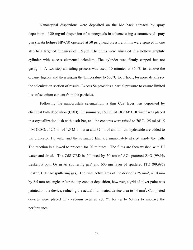
Nanocrystal dispersions were deposited on the Mo back contacts by spray
deposition of 20 mg/ml dispersion of nanocrystals in toluene using a commercial spray
gun (Iwata Eclipse HP-CS) operated at 50 psig head pressure. Films were sprayed in one
step to a targeted thickness of 1.5 μm. The films were annealed in a hollow graphite
cylinder with excess elemental selenium. The cylinder was firmly capped but not
gastight. A two-step annealing process was used; 10 minutes at 350°C to remove the
organic ligands and then raising the temperature to 500°C for 1 hour, for more details see
the selenization section of results. Excess Se provides a partial pressure to ensure limited
loss of selenium content from the particles.
Following the nanocrystals selenization, a thin CdS layer was deposited by
chemical bath deposition (CBD). In summary, 160 ml of 18.2 MΩ DI water was placed
in a crystallization dish with a stir bar, and the contents were raised to 70°C. 25 ml of 15
mM CdSO4, 12.5 ml of 1.5 M thiourea and 32 ml of ammonium hydroxide are added to
the preheated DI water and the selenized film are immediately placed inside the bath.
The reaction is allowed to proceed for 20 minutes. The films are then washed with DI
water and dried. The CdS CBD is followed by 50 nm of AC sputtered ZnO (99.9%
Lesker, 5 ppm O2 in Ar sputtering gas) and 600 nm layer of sputtered ITO (99.99%
Lesker, UHP Ar sputtering gas). The final active area of the device is 25 mm2, a 10 mm
by 2.5 mm rectangle. After the top contact deposition, however, a grid of silver paint was
painted on the device, reducing the actual illuminated device area to 14 mm2. Completed
devices were placed in a vacuum oven at 200 °C for up to 60 hrs to improve the
performance.
78

5.2.5 Characterization
Current-potential (I.V) characteristics were collected using a Keithley 2400
general purpose source meter and a Xenon lamp solar simulator (Newport) equipped with
an AM1.5 optical filter. Intensity of the light source was calibrated using a NIST
calibrated Si photodiode (Hamamatsu, S1787-08). Incident photon-to-electron conversion
efficiency (IPCE) measurements were collected as a measure of external quntuum
efficiency using an in-house fabricated spectrophotometer. Monochromatic light was
generated using a commercial monochromator (Newport Cornerstone 260 1/4M).
Generated light was chopped at 213 Hz and was focused to a spot size of 1 mm in
diameter on the active region. The response of the device was recorded at zero bias
between 300 and 1300 nm in 10 nm steps using using a lock-in-amplifier (Stanford
Research Systems, model SR830). The light intensity was calibrated using calibrated
photodiodes of silicon (Hamamatsu) and germanium (Judson).
Impedance characteristics of the photovoltaic cell were collected using a Solartron
1260A Frequency Response Analyzer coupled with a Solartron 1296 Dielectric Interface.
Measurements were taken between 0.1 Hz and 107 Hz with 5 steps per decade by
applying a 50 mV A-C waveform.
ICP-ms measurements were performed on digested solution of CIGS
nanoparticles in aqueous solutions. A 3 mg sample of the dry nanocrystals was digested
in 200 μL of highly concentrated nitric acid, and the digestion was allowed to proceed for
60 minutes. After which the resulting lime green solution was diluted 35,000x with 2%
nitric solution in DI water. Blank controls were prepared at all stages of the digestion,
and no significant concentration of desired elements was found in any of the blanks.
79

Analysis of purchased standards shows the measurements is accurate to parts per trillion
(PPT) levels, 5 orders of magnitude smaller than our measured concentrations.
XRD data was collected on a Bruker-Nonius D8 advance θ−2θ powder
diffractometer equipped with a Bruker Sol-X Si(Li) solid state detector and a rotating
stage. 1.54 Å radiation (Cu Kα) was used to collect at 0.01 increments of 2θ at a scan
rate of 6 °/min. XRD was collected on the absorber films that were subsequently
completed into devices.
X-ray photoelectron spectroscopy (XPS) spectra were collected using a Kratos
Photoelectron Spectophotometer equipped with a tungsten coil charge neutralizer, high
intensity monochromatic Al-kα X-ray source, and a 180 hemispherical electron energy
analyzer. The charge neutralizer was operated at constant 4.8 V during data collection.
Collected spectra were analyzed using CasaXPS software. Details of charge collection
and peak fitting are provided in the results section.
5.3 Selenization of CIGS Nanocrystals
Selenization of nanocrystal films took place inside a graphite box, Figure 5.1A-B.
The graphite box acts as a vessel to retain a positive pressure of selenium. Excess
selenium pellets were placed inside the box. The selenium pellets melt and evaporate
during the heating process, increasing the partial pressure of selenium in the processing
atmosphere. Nanocrystal films on Mo coated glass were placed inside the box with the
nanocrystal film facing away from the Se source. The box was sealed with a graphite
plug and placed in the central zone of a tube furnace, pictured in Figure 5.1C. The tube
furnace was sealed and purged with pure argon to achieve an inert atmosphere. The inert
80

atmosphere of the tube prevented undesired oxidation of the selenized film, and the box
limited loss of selenium from the nanocrystal films. The tube furnace was heated up to
selenization temperature (typically 500°C) for 60 minutes, and then cooled down to room
temperature. The graphite box was opened within an inert atmosphere glovebox and the
films were removed and saved in the glovebox prior to the CdS deposition step.
Figure 5.2A shows the XRD spectrums of CuInSe2 nanocrystals films on Mo
coated glass before and after selenization. The XRD reflection peaks associated with the
CuInSe2 layer become sharper after selenization, signaling a significant growth of the
grains. Cross sectional SEM images of the absorber layer before (Figure 5.2B) and after
(Figure 5.2C) selenization reveal extent of crystal growth. The common crystal growth
involved formation of a dense film of crystals at the absorber/back contact interface,
topped with amorphous byproduct. Under the selenization conditions, a layer of MoSe2
was observed to grow at the absorber layer and Mo interface. The MoSe2 provides an
ohmic contact between the new CIGS crystals and the remaining Mo back contact. The
presence of the MoSe2 layer is detectable through the XRD pattern of the selenized films,
Figure 5.2A. Formation and the impact of the MoSe2 layer are further discussed in
section 5.3.3.
81

Figure 5.1. (A) Side view and (B) cross-sectional view of the selenization box used for sintering of nanocrystal layers. The cylinder is capped with the plug to ensure buildup of a selenium partial pressure. (C) Tube furnace used for heating the selenization box.
82

Figure 5.2. (A) XRD pattern of CIS films before and after selenization, matching well with the estabulished crystal structure of CuInSe2 (PDF#97-006-8928) (B) SEM image of cross section of an as-deposited CuInSe2 film and (C) selenized CuInSe2 film.
Grain growth was essential to extract higher short circuit current density (Jsc)
from the absorber film. Light beam induced current microscopy (LBIC) measurements
had been previously used to characterize nanocrystal layers.18 LBIC technique was used
in this work to correlate morphology of the selenized film with increased photocurrent
from the selenized devices. Figure 5.3A shows the spatial SEM micrograph of a selenized
CuInSe2 film. Figure 5.3B shows the cross-sectional SEM image of the same absorber.
There is significant grain growth by selenization. For this film, however, grain growth
83

was confined to the back contact interface. At the same time, most of the new crystals
are capped with islands of amorphous byproduct. LBIC map of the final device, Figure
5.3C, reveals extensive heterogeneity in the photocurrent of the active region.
Figure 5.3. (A) Spatial and (B) cross section SEM image of selenized CuInSe2 film. (C) Shows the response of light beam induced current microscopy (LBIC) measurements and (D) flouresence microscopy image of device prepared with the selenized film. LBIC data courtesy of Micah Glaz.
LBIC maps of the active device layer reveal regions that are highly active and
regions which yield much smaller photocurrent. Comparing the SEM image of the
absorber layer (Figure 5.3A) to the LBIC map (Figure 5.3C), regions of high
photocurrent (represented by the higher potential bias) correspond closely with larger
grains. Regions with small photocurrent are either areas with exposed back contact or are
the amorphous byproduct. Cross-sectional SEM images (Figure 5.3B) show that there
84

are larger CIGS crystals under the amorphous byproduct, but these crystals are not active
in photocurrent generation.
Never the less, devices prepared with selenized absorber layers yield a much
higher Jsc under illumination. Figure 5.4A shows the current-potential (IV) response of
two devices prepared from the same set of CIGS nanocrystal inks. First device was built
using as-deposited nanocrystal film, as was discussed in chapter 2, with the
Au/CIGS/CdS/ZnO/ITO structure. The second device was spray deposited under
ambient conditions on Mo back contact and the absorber layer was selenized at 500°C
before incorporation into a working photovoltaic. The increased Jsc from 4.5 mA/cm2 to
13.5 mA/cm2 is indicative of better carrier collection in the selenized films.
Mott-Schottky measurements of the films, Figure 5.4B, reveal a modest reduction
of the doping density (NA) in the selenized absorber, from 2 x 10¹⁷/cm3 to 1 x 10¹⁷/cm3.
The reduced doping density results in a deeper space charge region (x) in the selenized
film. The improvements in Jsc is in line with the assumption that higher concentration of
the photogenerated carriers can be extracted with lower doping densities and larger grain
sizes. Overall series resistance of the devices, Figure 5.4C, does not change significantly
with the selenization process. The shunt resistance of the diode, however, is significantly
lower for the selenized device. The decrease in the shunt resistance, Figure 5.4D, is
mainly due to the poor coverage of the absorber layer across the full electrode area. The
exposed back electrode does not contribute to the photocurrent density of the devices, and
the shunting deteriorates fill factor of the devices. To fabricate a highly efficient device,
it is necessary to reduce void spaces in the selenized absorber layer.
85

Figure 5.4. (A) IV response of nanocrystalline and selenized CuInSe2 films. The nanocrystal device (denoted in blue) was built on Au back contacts, and the selenized device (denoted in red) was built based on the Mo back contacts. (B) Mott-Schottky response of the nanocrystal and selenized devices denotes a decrease in the doping density of the absorber layer with increasing grain sizes. The decrease in the doping density, combined with the improved mobility, increases the probability of collection for the photogenerated carriers. (C) Series resistance and (D) shunt resistance of the two diodes at different applied potentials.
The variation in spatial photocurrent density highlights the challenges to
fabricating higher efficiency devices. 1) What causes variations in grain growth, and how
does the growth pattern translate to final device efficiency. 2) What are the non-
crystallized regions in the selenized films and how do they impact the performance. And
3) what are the benefits and issues associated with the MoSe2 formation during
86

selenization. The following sections attempt to provide an overview of these variations
in the selenized films and how they impact the device efficiency of the selenized
nanocrystal layers.
5.3.1 Variations in selenization
Process of selenization has been extensively studied on metal and metal alloy
layers. The processing used here is better known as close-spaced vapor transport (CSVT)
selenization when applied to metal films.6 The CSVT process was used in lieu of other
selenization techniques, such as evaporation processing or H2Se treatment, because of
cost and safety. CSVT process was easy to implement and the chamber was confided to
reduce selenium leakage. The CSVT selenization is easy to reproduce and all the
variables involved with the selenization processes are controlled through temperature of
the selenization box. Several disadvantages are associated with this technique and are
discussed later in the section.
Selenization of metals and metal alloys with CSVT take place at relatively low
temperatures (< 420°C) and CuInSe2 grain growth is observed at temperatures as low as
240°C.12 For the selenization of CuInSe2 nanocrysals, however, no extensive grain
growth is observed at temperature below 350°C. CSVT process works at lower
temperatures because of the thermodynamically favorable incorporation of selenium to
form CuInSe2. Even though there is a 29 kJ/mol activation energy required for this
process,6 there is a 312 kJ/mol driving force toward formation of CuInSe2 from Cu and In
alloys.5 Since the selenium is already incorporated into the CuInSe2 nanocrystals, there is
no thermodynamic driving force for further incorporation of selenium into the absorber
film. As such, a much higher temperature is necessary to induce transport of the
87

constituent parts into larger grains. For the selenization of nanocrystal grains,
thermodynamic driving force involves forming larger crystal grains and reducing surface
states.
Selenization of nanocrystal grains into larger crystal structures did not yield
homogeneous layers of micron sized grains. Several studies were undertaken to promote
growth of the desired domains, while limiting growth of the undesired features. Several
key factors were determined to influence the selenization process. Temperature was the
key factor in determining growth, and the growth was observed with the selenizations at
or above 350°C. Secondly, the geometry of the selenization box controlled adhesion of
the selenized film to the back contact. And finally, the composition of the as-cast films
played an important role in determining the extent and morphology of grain growth in the
films.
Length of selenization, which plays an important role in selenization of metal
alloys, did not impact the extent of selenization of nanocrystal inks. Time does play a
significant role in the selenization of nanocrystals, but we did not observe any time
dependent performance variation. The length of time necessary for the selenization
chamber to heat up and cool down was longer than the kinetics of the process. A more
rapid selenization procedure is necessary to study the kinetics of CIGS grain growth.
Figure 5.5 shows SEM images of CuInS2 nanocryal films selenized at different
temperatures. At 350°C larger features are visible on the surface of the nanocrystal layer,
and these features are most likely the starting seeds for recrystallization of the CuInSe2
nanocrystals into larger crystals. Bulk of the film, however, remains as nanocrystals as is
evident in cross sectional SEM image, Figure 5.5B. At 400°C, the surface features have
88

grown larger, and have started to coalesce into larger grains; at the same time, it is
evident that a layer of crystals have started forming at the Mo and nanocrystal interface.
The two sections of growth are separated by a nearly continuous layer of amorphous by-
product of the selenization. At 500°C, majority of the film is recrystallized into larger
grains, but several pockets of the amorphous by-product remain. The kenetics of the
MoSe2 formation prevents higher temperature selenziation. Reaction of the back contact
with the selenium vapor leads to delamination of the back contact at higher temperatures,
more on this topic in section 5.3.3.
The higher growth temperatures required to sinter nanocrystalline CIGS crystals
into larger grains is understandable. There is a large thermodynamic driving force to
form CIGS from the constituent metals, as such, the kinetics of the reaction are relatively
rapid at lower temperatures to selenize the metallic films. Since the CIGS crystal is
already present in the nanocrystal ink, the driving force is no longer there;. The growth
of nanocrystals at this stage resembles the growth of CIGS from CuSex and InSex
precursors. These sub-phases form rapidly during the selenization of the metal alloys,
and they diffuse to form larger crystals.13 A similar mechanism is dictating the growth of
larger crystals in the nanocrystal layer, the CIGS structure could be decomposed to
substituent binary products (CuSex, InSex and GaSex) which diffusing to supply larger
grains. The diffusion requires a much higher processing temperature than the formation
of CIGS from precursor metals.
89

Figure 5.5. SEM of the surface and the cross-section of selenized CuInS2 nanocrystal films at different temperatures, (A-B) 350°C, (C-D) 400°C, and (E-F) 500°C. (G-H) Correspond to CuInS2 particles selenized at 500°C but the as-deposited nanocrystal film was treated with hydrazine solution before selenization.
Construction of the selenization box further dictates the uniformity of the
selenization process. Figure 5.6 shows SEM images of two identical CIGS nanocrystal
films selenized under the same conditions in two different boxes. First box had a loose
90

fitting cap and while it remained sealed during the selenization process, it was not air-
tight. The second box, had a much tighter seal, and it remained air-tight throughout the
selenization process. In the first case, Figure 5.6A-B, the absorber layer peeled during the
selenization process, revealing the back contact underneath. The peeling is due to buildup
of residual stresses during the selenization process and adhesion failure between the
CIGS crystals and the back contact. Since exposed back contact does not have any
photon-absorbing material, the peeled regions are not contributing to the overall Jsc of the
devices, as evident in the LBIC map, Figure 5.3C. Selenization in the air-tight box
resulted in films that had similar extent of grain growth, Figure 5.6C-D, but adhered
much more uniformly to the back contact. The improved uniformity of the resulting film
constitutes a doubling of the overall efficiency of the device, stemming from higher Jsc
and better FF in the device. The exact reason behind the differences in adhesion is still
unclear, but must be attributed to the movement of the selenium vapor within the
chamber. The air-tight box has minimal drift current of the selenium vapor, while the
leaky box is loosing selenium into the furnace. The leaky box creates a flow of selenium
through the box. The peeling of absorber layer is not unidirectional, ruling out direct
flow resistance as the cause of peeling. The difference could be due to residual oxygen
present in the chamber during selenization. Mild oxidation of the back contact takes place
in the tightly sealed box. In the leaky box, the flow of fresh selenium purges the process
box, reducing possible oxidation. If the oxidized surfaces are more adhesive, there would
be greater tolerance of stresses between the two layers. This hypothesis is under further
investigation.
91

Figure 5.6. SEM of the surface of selenized CIGS nanocrystals at 500°C (A-B) inside a leaky box or (C-D) in a tightly sealed box.
A third variable determining the morphology and the extent of grain growth
during the selenization process was the composition of the starting nanocrystalline film.
Cu:In ratio in the nanocrystal inks determined the growth pattern. Figure 5.7 illustrates
the pattern of crystal growth for three different nanocrystal sets. First selenization set,
Figure 5.7A-D, was CuInSe2 nanocrystal ink synthesized using TCI oleylamine as the
solvent and capping ligand during reaction. Based on ICP-ms analysis of the reaction
product, the Cu:In ratio was 1:1.55. TEM images of the particle set, Figure 5.7A, reveals
irregularly shaped particles. Once selenized at 500°C, the film had extensive grain
growth at the back contact interface, mainly in shape of pyramids placed on the surface.
Majority of the crystal growth, however, was covered by the presence of the amorphous
byproduct. The efficiency of the devices built with this composition nanocrystals, Figure
5.7D, was limited to under 0.3% PCE.
92

Second product contained CuInSe2 nanocrystals synthesized using Corsitech
oleylamine. Based on ICP-ms analysis, the Cu:In ratio in the ink was 1:1.25. TEM image
of the nanocrystal product, Figure 5.7E, reveals nearly spherical products. The resulting
selenized film at 500°C reveals crystal growth at two junctions, the nanocrystal/back
contact junction and the nanocrystal/ambient junction. The two areas of grain growth are
separated with a semi-continuous film of the amorphous byproduct. Devices prepared
with this film, Figure 5.7H, exhibit efficiencies consistently above 1% PCE.
Third ink investigated contained CuInS2 nanocrystals synthesized using TCI
oleylamine. ICP-ms measurements of the Cu:In ratio was 1:0.88 for this set of inks. The
TEM image of the nanocrystals, Figure 5.7I, show irregular hexagonal disks. The
resulting film after selenization at 500°C has higher coverage of the larger crystals on the
surface, Figure 5.7J, with larger crystals distributed throughout the depth of the film.
Devices built from this particle set, Figure 5.7L, had efficiencies consistently above 2%
PCE. The SEM of the selenized film, Figure 5.7J-K, reveals two types of crystal growth.
The shapeless growths that indicate the CuInSe2 crystals dominate the landscape, but
there are several irregularly shaped hexagons that protrude above the surface. These
shapes visible in SEM images might be indicative of excess Cu forming CuSex disks.
XRD spectra of the selenized films reveal no crystalline byproduct forming with the
selenization of the CuInSe2 films.
Different morphologies are produced due to differences in position and extent of
nucleation in the nanocrystal films. In the highly indium rich product, Figure 5.7A, had
very limited nucleation sites; exclusively on the back contact. The less indium rich
product exhibited nucleation at the back contact, but had few nucleation points on the
93

surface. Finally, the indium poor product, Figure 5.7I, had nucleation points distributed
throughout the depth of the film. All three films had similar concentration of the
amorphous byproduct distributed though the selenized film.
Placement of nucleation points are important for selenization of vapor deposited
Cu and In alloys. Most commonly used technique for vapor deposited samples involves a
“two step” process.14 For initial growth stage, it was important to form a indium poor
region (usually in the Cu:In ratio of 1:0.8) for the initial seeding of crystals.6 Similar
nucleation mechanics might be dictating the crystal growth in the selenization of
nanocrystal inks as well. In the highly indium rich starting inks, nucleation of new
crystals is limited to the back contact, where the crystalline backcontact can act as a
nucleation site with access to Na, from the soda lime substrate, can promote larger crystal
growths.15 In the slightly indium rich starting ink, in addition to the back contact,
nucleation of larger grains takes place at the ambient interface, where outgassing of
In2Se36 results in regions of indium deficiency. But in the indium poor starting product,
nucleation happens along a whole depth of the film. As was observed from the LBIC
measurements, Figure 5.3C, larger grains at the top surface are the only grains active at
supplying the short circuit current density. Synthesis and selenization of CuInSe2
nanocrystal inks with overall Cu:In ratio very close to 1:1 is necessary to further
investigate the nucleation events.
Two other differences can impact the crystal growth, 1) composition of organic
ligand in nanocrystal ink, and 2) replacement of sulfur with selenium in the crystal
structure. The organic ligand takes up a large volume fraction of the as deposited films,
and with the removal of the organic residue during the selenization process, a large
94

reduction in the total volume takes place. The reduction is responsible for some of the
cracking in the selenized films, Figure 5.3A. Crystal expansion with replacement of
sulfur atoms with selenium in the CuInS2 structure was studied in previous literature.4
While both differences could impact final device efficiency, there is little evidence that
they are responsible for the nucleation pattern in the films.
Figure 5.7. TEM images of as-synthesized nanocrystals, surface and cross-sectional SEM of the selenized films and IV response of the fabricated devices with 500°C selenized nanocrystal absorber layers. (A-D) high indium excess CuInSe2 nanocrystal grains, (E-H) lower indium excess CuInSe2 nanocrystal grains, and (I-L) indium deficient CuInS2 nanocrystal grains. TEM images courtesy of C. Jackson Stolle.
95

Figure 5.8. (A) Surface SEM and (B) cross-sectional SEM of CuInS2 nanopraticles baked at 500°C and then selenized at 500°C.
Further In deficiency could be achieved by pre-baking the indium poor CuInS2
nanocrystal films at 500°C, followed by selenization at 500°C. Figure 5.8 shows spatial
and cross-sectional SEM images of the resulting film. Nucleation in this film is much
more wide spread than the unbaked selenization presented in Figure 5.7J-K and as a
result, the crystals grown are on average smaller. Devices built from pretreated and then
selenized films, however, had lower efficiencies. The deterioration in efficiency was
mostly due to higher shunting in the device. The shunting was due to the high
concentration of CuSex byproduct. Presence of higher concentration of geometrically
shaped crystal plates on the surface of the selenized films is indicative of the higher
degree of formation for this sub-phase. For vapor deposited samples, KCN etches are
96

usually performed to etch out the undesired CuSex regions. Etching adds another step to
device fabrication and was avoided in this work. A route was sought to create more
efficient device performance without the need for secondary processing of the absorber
layers.
5.3.2 Characterization of the amorphous layer
LBIC maps of the completed devices, Figure 5.3C, reveals how different parts of
the absorber layer contribute to the photogenerated current. One of the limiting factors
identified is the “unsintered” regions that do not contribute to the photocurrent of the
devices. The “unsintered” over layer limits the output of the sintered crystals in two
ways. First, the over layer absorbs a fraction of the incident photons, limiting the incident
radiation accessible to the sintered grains. Secondly, the presence of the amorphous layer
hinders formation of an uninhibited junction between the CIGS absorber and the other
layers. XPS spectroscopy of the selenized films were utilized to understand the
composition and the oxidation state of the amorphous regions in an attempt to design
selenized layers without the amorphous regions that hinder the overall device
performance.
Figure 5.9A shows cross sectional SEM image of a selenized CIGS layer. In this
case, the crystal growth has taken place exclusively at the back contact interface, and the
surface of the crystals is covered by the amorphous layer. XPS measurements of this film,
Figure 5.9B, reveal that the composition of the amorphous layer is comprised exclusively
of a carbon and selenium mixture. Sputtering of this surface layer with high energy Ar
97

atoms reveals that the underlying crystal structure is comprised of the Cu, In and Ga of
the starting nanocrystal ink, as these indicative peaks appear with further sputtering.
Figure 5.9. (A) Cross-sectional SEM image of a selenized CIGS film, coverage of the amorphous layer on the surface of the selenized crystals limits the performance of the fabricated devices. (B) XPS spectrum of the as-selenized CIGS layer before and after Ar sputtering. Sputtering of the surface layer with high energy Ar exposes the crystalline structure underneath the surface layer of carbon and selenium. The underlying layer had similar composition to that of the starting nanocrystals.
Figure 5.10 shows the high resolution XPS spectra of the CIGS film. The
charging for the samples was corrected by shifting the In 3d5/2 peak to binding energy of
444.4 eV, which is indicative for indium in the CIGS structure.16 All the other peaks
were shifted with respect to the indium peak. The C 1s peaks indicate that the resulting
98

carbon present in the top layer is nearly identical to the carbon present on the surface of
the as-deposited nanocrystal inks layer. In the case of the as-deposited inks layer, the
main peak of the carbon falls at 285.0 eV, which is indicative of hydrocarbons present on
the surface;16 but with the selenization, the main peak of the carbon shifts to a slightly
lower binding energy of 284.5 eV, indicating the carbon has taken on a more graphitic
nature. The total composition of the carbon on the surface increases with selenization,
indicating that the free capping ligand in the film migrates to the surface to be evaporated
and taken away. The oleylamine capping ligand is not fully removed at 500°C
selenization. Attempts at removing the oleyalmine capping ligand prior to selenziation
was undertaken through chemical treatment with hydrazine. The selenized hydrazine
treated films, Figure 5.5G-H, contain much smaller fractions of the amorphous sections.
There was, however, little improvements in the overall efficiency of the device when the
films were hydrazine treated before selenization.
The Se 3d region of the XPS spectrum, Figure 5.10, reveals deposition of
elemental selenium on the surface of the selenized layer. Selenium in the as deposited
nanocrystal film has binding energy at 54 eV, and the peak can be deconvoluted into the
two spin states of selenium. This position is in good accordance to the value for selenium
binding energy in vapor deposited CIGS structure.16 After selenization, the Se peak
shifts to higher binding energy of 55 eV. This bonding energy corresponds to elemental
selenium.16 Selenium is deposited on the surface of the selenized films by condensation
of the selenium vapor during the cool down of the selenization box. Deposition of
elemental selenium on the surface is detrimental to device performance and must be
removed to promote good junction formation between the CIGS and CdS layers.
99

Thermal treatments are known to remove elemental selenium without hindering the
performance of the CIGS device.17 Figure 5.10 shows evolution of the selenium peak
with post-selenization thermal treatment at different temperatures. Thermal annealing is
able to remove a fraction of the elemental selenium, but even at 300°C some of the
deposited elemental selenium remained. At the same time, the post treatments is unable
to remove any of the remaining carbon on top of the selenized film. Little improvement
in the overall device efficiency was observed with the removal of the elemental selenium.
The limiting factor remains the presence of the carbonaceous film.
Figure 5.10. High resolution XPS scans of In 3d5/2, C 1s and Se 3d regions of CIGS
films before and after selenization at 500°C. Post-baking of the selenized absorber layers for 60 minutes at different temperatures removed some excess elemental selenium but a majority of the carbonaceous material remained. All the peak intensities are normalized for easier viewing.
100

5.3.3 Formation of MoSe2
XRD spectrum of the selenized film, Figure 5.2, shows formation of a secondary
set of peaks at 31.8° and 56.2° 2θ values which do not correspond with the CuInSe2 or
the Mo back contact. The presence of these peaks indicates formation of MoSe2 at the
interface of the back contact and the absorber materials. MoSe2 is a semiconductor and
is deemed necessary to form high efficiency CIGS devices.10 As was discussed in
chapter 2, the lack of the MoSe2 layer creates an electronic barrier between as-deposited
CIGS nanocrystal films and Mo back contact. MoSe2 is necessary to form an ohmic
contact between the absorber materials and the Mo back contact. Formation of the
MoSe2, however, brings up several issues associated with the selenization process.
Figure 5.11A shows representative EDS line-scan results running across the depth
of a selenized Mo back contact. The presence of the Se along the length of what is
considered the back contact shows how much of the Mo present has reacted with the
selenium vapor. SEM images of the back contact (Figure 5.11B), shows the 1 µm thick
Mo back contact has ballooned into 3 µm through the selenization process. Selenization
at 500°C left only 200 nm of Mo metal serving as the back contact. Cross-sectional SEM
images of the devices annealed at different temperatures, Figure 5.5, reveals the extent of
Se incorporation and MoSe2 growth is temperature dependent. At 350°C, very little of
the Mo has reacted to form MoSe2, but at temperatures above 500°C the entire Mo back
contact reacts. Once there is no more metallic Mo left adhering to the glass substrate, the
film starts to peel away, and devices can no longer be fabricated. This is one issue
limiting the selenization procedure to < 500°C.
101

Another issue with the reaction of Mo and formation of MoSe2 is the increased
resistance of the devices. MoSe2, as a semiconductor, has much lower conductivity than
the Mo metal. As more of the Mo metal is used up, the series resistance of the devices
increases. The increased series resistance reduces the efficiency of the device. The
formation of several microns of MoSe2 is the reason the series resistance of the selenized
devices are on par with the nanocrystalline absorber devices, Figure 5.4C.
Figure 5.11. (A) EDS line-scan across the (B) cross-sectional SEM of the Mo back contact selenized at 500°C and fabricated into a device. EDS indicates that the majority of the back contact has large concentrations of Se incorporated in with the Mo.
5.4 High Efficiency Selenized Nanocrystal CIGS Devices
Table 5.1 lists best device efficiencies achieved with selenization of different
composition CIGS nanocrystal films. Best efficiency devices were fabricated using
nanocrystals with targeted composition of CuIn0.5Ga0.5Se2. The IV response of this
device is shown in Figure 5.12A. External quantum efficiencies (EQE) measurements,
Figure 5.12B, indicate over 50% of the absorbed photons were extracted as current for a
102

wide range of visible wavelengths. Jsc calculated based on the EQE measurements was
20.3 mA/cm2, matching well with the Jsc measured from the IV results at 20.1 mA/cm2.
Based on ICP-ms analysis, the measured Ga/(In+Ga) was close to 32% in the as-
deposited nanocrystal films. The Ga/(In+Ga) was very close to the 30% observed to
produce the highest efficiency vapor deposited CIGS.10 The Cu:In ratio was measured at
1:0.8, which was very similar to the observed ratio discussed in section 5.3.1 that led to
formation of high density of nucleation points in the nanocrystalline films. Presence of
the gallium allows for the indium deficiency to exist, but is incorporated into the crystal
structure to limit the formation of the undesired CuSex sub-phase. At the same time,
gallium content enables targeting a specific electronic bandgap to optimize the Voc of the
device. Similarly selenized films but with different starting nanocrystal CIGS
composition, Table 5.1, yielded lower efficiency devices.
Table 5.1. Measured composition of nanocrystal inks based on ICP-ms analysis for
targeted x in Cu(In1-xGax)Se2 relative to the concentration of Cu present and the best device characteristics based on selenized films of the nanocrystal films.
Measured Composition Device Characteristics Target x (%) Cu In Ga Se
Voc (mV)
Jsc (mA/cm2)
FF PCE (%)
0 1.00 1.55 0.00 2.70 227 2.77 0.29 0.18 15 1.00 1.59 0.05 2.87 240 8.50 0.34 0.69 25 1.00 1.06 0.14 2.28 320 13.59 0.36 1.56 50 1.00 0.83 0.39 2.33 526 20.10 0.48 5.10 75 1.00 0.49 0.82 2.53 478 9.08 0.35 1.51 100 1.00 0.00 1.29 2.46 205 1.81 0.28 0.10
103

Figure 5.12. (A) IV response of the best efficiency selenized device, (B) IPCE measurement of this device, (C) optical image of the full device, with the painted silver contacts, and (D) SEM of the absorber layer of the selenized film.
Impedance measurements of the highest efficiency selenized device, Figure 5.13,
shows doping density in the selenized film to be around 1017/cm3. This doping density is
an order of magnitude higher than what is achieved in vapor deposited samples.10
Reduction of the doping density even further presents an opportunity for achieving higher
efficiency devices.
104

Figure 5.13. (A) Fit of model circuit to impedance measurement of the device at zero bias. (B) Doping characteristics of selenized nanocrystalline films as determined through Mott-Schottky analysis of the impedance results.
5.4.1 Role and purity of CdS layer
As discussed earlier in chapter 3, the photoactivity of the CdS layer plays an
important role in electronic band alignment of the device under illumination. Similar
trends were observed with the selenized nanocrystal absorber layers. Furthermore, it was
discovered that the purity of the precursors necessary for CdS deposition were critical to
achieving highly efficient devices. High doping levels in CdS increases the barrier to
electron extraction from the absorber layer. The deterioration in efficiency due to
impurities in CdS was observed in the fill factor (FF) of the final devices. Figure 5.13
illustrate the IV response under AM1.5 illumination of two similarly selenized CIGS
105

films, with differences in the DI water used for the chemical bath deposition of the CdS
layer. When higher impurities were present in the DI water, an inversion in the IV sweep
at 200 mV resulted in unrealistically low FF in the devices of 0.21. Using highly purified
DI water, 18.2 MΩ, resulted in elimination of this inversion and achieved much better FF
for the device at 0.38.
Figure 5.14. Representative IV response under AM 1.5 illumination for devices prepared with different purity CdS layers. The purity of the CdS layer was controlled through the purity of the DI water used. Higher resistance of the water indicates the higher purity of the water.
5.4.2 Retaining flexibility in device architecture
One benefit of using nanocrystalline inks as the precursor for photovoltaic devices
involves the flexibility of architecture and design as was illustrated in Chapters 2 and 3.
The selenization process significantly reduces the design parameters available for
fabrication. One of the goals of this work was to use flexible substrates for device
fabrication. Retaining the ability to build lightweight and flexible devices would
significantly promote the commercial outlook for this process. Figure 5.15 shows
preliminary results of selenized absorber devices on flexible substrates. Devices could be
106

built on both kapton, Figure 5.15A, or stainless steel, Figure 5.15B, substrates. The
flexibility of the final device structure was much poorer than the unselenized absorber
layers discussed in chapter 2 and the device efficiencies achieved on the flexible
substrates were considerably lower than what was achieved on soda lime glass substrates.
Figure 5.15C shows a representative IV response of selenized nanocrystal CIGS devices
built on stainless steel substrate. Further work is necessary to understand the limitations
of building selenized photovoltaics on flexible substrates and attempt to overcome these
challenges.
Figure 5.15. Images of flexible devices fabricated on (A) kapton and (B) stainless steel. (C) IV response of flexible device fabricated on stainless steel substrate.
107

5.4.3 Engineering electronic bandgap based on Ga content of nanocrystal inks
One of the advantages of the CIGS as photovoltaic absorber materials is the
ability to target a specific electronic bandgap by targeting a specific ratio of Ga to In in
the crystal structure. The ability to control the bandgap through the nanocrystal inks
synthesis enables creation the whole spectrum of bandgap energies accessible to CIGS.
Table 5.1 lists measured composition of the starting nanocrystal inks for different
targeted compositions. Figure 5.16 demonstrates the shift in the <112> reflection of the
XRD pattern as more Ga is incorporated into the crystal before and after selenization.
The shift to higher 2θ values are indicative of the smaller element (Ga) replacing a larger
element (In) in the crystal structure. Smaller element reduces the lattice constant and
increases reflection angle in accordance to Bragg’s law. The selenization of the crystals
increase the sharpness of the reflection peak, indicating growth to larger crystal sizes.
The central position of the peak, however, is retained, indicating the crystallographic
structure of the as-deposited and the selenized films are the same. Figure 5.16C shows the
IPCE measurements of the selenized absorber devices, the effective band edge of the
devices changes according to the targeted composition of the nanocrystals.
Figure 5.17 shows the measured bandgap of the selenized nanocrystaline absorber
layers with different Ga concentrations in the starting nanocrystal inks. Comparison to
the bandgap values of vapor deposited CIGS with varying Ga concentration8 reveals
similar trends shared between the two sample sets. The differences between the
measured badgap of the selenized nanocrystal absorbers and the vapor deposited absorber
is due to the measuring technique used in each case.
108

Figure 5.16. <112> reflection of the XRD pattern for gallium CIGS nanocrystals (A) as cast and (B) after selenization. (C) IPCE measurement of the devices built from selenized films of different Ga CIGS.
Figure 5.17. Bandgap measurements for the selenized nanocrystal films with different Ga content as determined through IPCE measurements compared to vapor deposited film bandgap measured by fluorescence.8
5.5 Summary
Post deposition treatment strategies were explored to increase charge mobilities
and reduce doping densities for higher efficiency devices. At 3% PCE, the as-deposited
nanocrystal absorbers are not efficient enough for commercialization. Post deposition
selenization of CIGS nanocrystal films at 500°C enables efficiencies up to 5.1% PCE.
109

Several challenges were identified with the selenization process and methods were
discussed to resolve these issues and increase the efficiency of the devices even further.
Extent of selenization was strongly impacted by the composition of the starting
inks. Extent and morphology of sintering determined the efficiency of the final device.
LBIC technique was utilized to characterize specific regions of device and optimize the
source of photocurrent. The Ga/(In+Ga) composition determined the bandgap of the
materials, and was important to optimize the Voc of the selenized absorber devices. It
was demonstrated that selenized nanocrystals with specific Ga concentration had a
bandgap energy that matched well with the bandgap of vapor deposited samples with
similar Ga concentration. Secondly, Cu:In ratio determines the extent of selenization and
the mechanics of crystal growth. A Cu rich nanocrystal film was necessary to seed
multiple sites for crystal growth but avoid formation of undesired CuSex subphases that
act to deteriorate device performance.
The selenization process is not favorable to retain the flexibility of architecture
demonstrated for as-deposited nanocrystal devices. It was, however, demonstrated that
devices on flexible substrates are possible with selenized nanocrystal absorber layers.
Further optimization in processing is needed to further improve the efficiency of these
devices. More studies are necessary to understand the mechanics of crystal growth in the
nanocrystal films. Lower temperature selenization processes can be devised to fabricate
higher efficiency devices on flexible substrates.
110

5.6 Notes and References
1. V.A. Akhavan, M.G. Panthani, B.W. Goodfellow, D.K. Reid, B.A. Korgel, Energy Express 18 (2010) A411–A420.
2. V.A. Akhavan, B.W. Goodfellow, M.G. Panthani, D.K. Reid, D.J. Hellebusch, T. Adachi, B. A. Korgel, Energy and Environmental Science 3 (2010) 1600–1606.
3. C. Steinhagen, V.A. Akhavan, B.W. Goodfellow, M.G. Panthani, J.T. Harris, V.C. Holmberg, B.A. Korgel, ACS Appl. Mater. Interfaces 3 (2011) 1781–1785.
4. Q. Guo, G.M. Ford, H.W. Hillhouse, R. Agrawal, Nano Lett. 9 (2009) 3060–3065.
5. S.T. Lakshmikumar, A.C. Rastogi, Appl. Phys. Lett. 66 (1995) 3128–3130.
6. A. Parretta, M.L. Addonizio, S. Loreti, L. Quercia, M.K. Jayaraj, J. Crystal Growth 183 (1998) 196–204.
7. M.A. Green, K. Emery, Y. Hishikawa, W. Warta, Prog. Photovolt: Res. Appl. 18 (2010) 346–352.
8. M.I. Alonso, M. Garriga, C.A. Durante Rincon, E. Hernandez, M. Leon, Appl. Phys. A 74 (2002) 659–664.
9. M.G. Panthani, V. Akhavan, B. Goodfellow, J.P. Schmidtke, L. Dunn, A. Dodabalapur, P.F. Barbara, B.A. Korgel, J. Am. Chem. Soc. 130 (2008) 16770–16777.
10. I. Repins, M. Contreras, M. Romero, Y. Yan, W. Metzger, J. Li, S. Johnston, B. Egaas, C. DeHart, J. Scharf, B. E. McCandless, R. Noufi, "Characterization of 19.9%-efficient CIGS absorbers", presented at Photovoltaic Specialists Conference, 2008. PVSC '08. 33rd IEEE, 11-16 May 2008, 2008.
11. H.W. Schock, Solar Energy Mater. Solar Cells 35 (1994) 19.
12. S.T. Lakshmikumar, A.C. Rastogi, J. Appl. Phys. 79 (1996) 3585–3591.
13. J. Ermer, R. Gay, D. Pier, D. Tarrent, J. Vac. Sci. Technol. A 11 (1993) 1888–1895.
14. N.G. Dhere, K.W. Lynn, Solar Energy Materials and Solar Cells 41-42 (1996) 271–279.
15. U. Rau, M. Schmitt, F. Engelhardt, O. Seifert, J. Parisi, W. Riedl, J. Rimmasch, F. Karg, Solid State Communications 107 (1998) 59–63.
16. C. Calderon, P. Bartolo-Perez, O. Rodriquez, G. Gordillo, Microelectronics Journal 39 (2008) 1324– 1326.
111

112
17. R. Hunger, T. Schulmeyer, A. Klein, W. Jaegermann, K. Sakurai, A. Yamada, P. Fons, K. Matsubara, S. Niki, Surface Science 557 (2004) 263–268.
18. D.P. Ostrowski, M.S. Glaz, B.W. Goodfellow, V.A. Akhavan, M.G. Panthani, B.A. Korgel, D.A. Vanden Bout, Small 6 (2010) 2832–2836.

Chapter 6: Conclusions
The technological barrier to photovoltaic (PV) electricity remains the high cost of
PV module production. Reliance on silicon as the photon absorbing material and the
high temperature processing dictate high production costs for today’s PV technology.1
PV devices that produce electricity at competitive costs with conventional forms of
electricity are not yet available. An order of magnitude reduction in module production
costs but retaining > 10% power conversion efficiency (PCE) is necessary to design the
next generation PV devices that could compete with conventional forms of electricity
generation. This work demonstrated a new route to fabricate viable PV devices using
Cu(In1-xGax)Se2 (CIGS) nanocrystal inks deposited under ambient conditions.2
Nanocrystal inks provide a novel way to deposit thin films of inorganic materials
without thermal or vacuum treatments. Synthetic procedure for CIGS nanocrystal inks
was established by Matthew Panthani and collegues.3 A spray-deposition process was
devised to deposit CIGS nanocrystal layers rapidly and inexpensively under ambient
conditions. The layers were then incorporated into functioning devices with reliable and
robust PV response. The device efficiencies achieved to date, however, have been
relatively low. Without high temperature selenization of CIGS nanocrystal films, PCEs
of just above 3% were demonstrated.4 Commercial application of these materials
requires further improvements in device efficiency. Nonetheless, low temperature
solvent-based processing of nanocrystal layers enabled a variety of different material
combinations, PV device architectures and substrates that are not possible with high
temperature processing.
113

The main weakness of nanocrystal-based PVs is the inability to extract significant
photocurrent. Electron/hole trapping and poor charge mobility limits the overall
efficiency of the devices. Carriers could not be efficiently extracted from nanocrystal
layers thick enough for optimum photon absorption characteristics. Best efficiency
devices were fabricated from nanocrystal devices with less than 200 nm thickness of
absorber layer. The thinner devices were not able to absorb a high fraction of the
incident spectrum, but converted > 50% of the absorbed photons to electricity as
measured by internal quantum efficiency (IQE) calculations. Higher photocurrents were
achieved by stacking multiple junctions with transparent top and bottom contacts, but
thus far, the total device efficiency has remained low.2
A combination of synthetic variations and low temperature treatments were
investigated to improve collection depth in the nanocrystal layers. These strategies,
however, did not result in noticeable improvements in overall device efficiency. For
example, hydrazine treatment of as deposited nanocrystal inks removed a fraction of the
insulating oleylamine capping ligands, and improved mobility through the nanocrystal
film, but the final device efficiencies were lower due to creation of carrier trap sites by
removing the capping ligand. Further work is necessary to improve upon these strategies.
Perhaps combinations of nanocrystals and 1-D nanorods or nanowires5 could reduce the
hopping in the nanocrystal films, or the formation of a bulk heterojunctions with greater
interfacial contact between n- and p-type semiconductor layers could lead to better charge
collection. Colloidal nanocrystal inks can be deposited under a variety of conditions,
providing the means to devise more exotic device geometries. Fabricating low-cost and
high efficiency PV devices from as-deposited nanocrystal inks provides the best
114

opportunity for commercialization, but further research is necessary to design better inks
and better device geometries for this purpose.
Another route to fabricate PV devices based on nanocrystal inks deposition
involved selenization of the deposited inks to fabricate larger grain devices. Higher
carrier mobility and lower doping levels in larger grains overcame the extraction issues
encountered with the nanocrystalline grains. Selenization process enabled fabrication of
devices with similar efficiencies to vapor deposited samples, but with lower deposition
costs. This process retained much of the device architecture and limitations associated
with vapor deposited devices, but provided a model for understanding charge collection
and mechanics of crystalline grain growth. Hilhouse, Agrawal and coworkers6-8 have
shown that high temperature selenization of CIGS-based nanocrystal films can lead to
efficiencies comparable to vapor-deposited CIGS devices. My work aimed at identifying
milder processing conditions to grow crystalline grains, understand the growth process
and further improve device efficiencies.
Selenization of nanocrystalline grains was similar to selenization of vapor
deposited metal alloys in some aspects and different in others. The grain growth turned
out to be critically dependent on the composition of the starting precursor film and
similar to vapor deposited samples, high efficiency devices were fabricated from a
narrow range of compositions. At the same time, the thermodynamic driving forces
promoting growth of vapor deposited CIGS did not promote grain growth in the
nanocrystalline films. As such, higher temperatures were necessary to form dense
network of selenized CIGS grains from nanocrystal precursors.
115

The ratio of Cu:In in the nanocrystal films impacted the growth pattern during
selenization. A Cu/In above one was necessary to seed grains, but copper excess led to
formation of CuSex byproduct that shunted the absorber layer. A copper deficiency was
achieved by including gallium in the starting product. While grain growth is responsible
for higher carrier mobility and better charge extraction, the placement of the larger grains
was critical for charge collection. Light beam induced photocurrent maps (LBIC) were
used to identify photoresponse of different regions of the selenized film. Presence of a
carbonaceous byproduct film complicated the growth pattern and produced microscopic
heterogeneity in the selenized devices. Only the larger grains on the surface were found
to actively contribute to the photocurrent from the device.
Similar to vapor deposited CIGS, the Ga composition in the starting film was
shown to determine the bandgap of the selenized absorber layers. Measured bandgap
values matched well with what has been reported in vapor deposited samples.
Optimizing all variable (composition, selenization apparatus and selenization
temperature) resulted in selenized nanocrystal CIGS devices with 5.1% efficiency and
short circuit current densities above 20 mA/cm2.
To design PV devices using CIGS nanocrystalline inks, LBIC9 and
photoelectrochemical (PEC)10 measurements were used to accelerate design and
implementation new ideas. They will play an important role in future discoveries. Future
work requires developing lower temperature or more rapid sintering routes to increase the
grain size in as-deposited films. This kind of processing should be enabled by the
predetermined crystal structure and composition available through nanocrystal inks
deposition. Avoiding addition of excess selenium reduces the processing costs and
116

complexity. To achieve higher efficiencies, larger and more interconnected grain
structure is needed to absorb more photons and extract more carriers. Selenization is the
only viable option for now, but it remains a barrier to less expensive device fabrication.
Figure 6.1. Progress timeline for solution processed CIGS devices by ambient deposition of CIGS nanocrystal inks.
Over the past five year, there has been a steady improvement in the demonstrated
efficiency of photovoltaic devices fabricated by solution deposition of CIGS nanocrystal
inks, Figure 6.1. The main driving force behind the improvement has been a steady
march towards reduced impurities in the semiconductor layers, and improved
conductivities of electrode materials. Doping levels in the mid to low 1017/cm3 are now
achieved in both the nanocrystal absorbers and selenized nanocrystal absorbers. Series
resistance of the fabricated devices are now in 100–150 Ω/cm2 range. Devices efficiency
could be further improved by reducing the absorber layer doping density to low 1016/cm3,
117

118
and reduce total series resistance of the devices below 10 Ω/cm2. A disruptive
breakthrough is still necessary to promote this technology to the rank of a commercially
viable PV fabrication techniques. Because of the low cost of deposition and the
flexibility of device architecture associated with ink based deposition, further interest in
this technology is likely.
6.1 Notes and References
1. V.A. Akhavan, B.W. Goodfellow, M.G. Panthani, B.A. Korgel, Modern Energy Review 2 (2010) 27–29.
2. V.A. Akhavan, B.W. Goodfellow, M.G. Panthani, D.K. Reid, D.J. Hellebusch, T. Adachi, B. A. Korgel, Energy and Environmental Science 3 (2010) 1600–1606.
3. M.G. Panthani, V. Akhavan, B. Goodfellow, J.P. Schmidtke, L. Dunn, A. Dodabalapur, P.F. Barbara, B.A. Korgel, J. Am. Chem. Soc. 130 (2008) 16770–16777.
4. V.A. Akhavan, M.G. Panthani, B.W. Goodfellow, D.K. Reid, B.A. Korgel, Energy Express 18 (2010) A411–A420.
5. C. Steinhagen, V.A. Akhavan, B.W. Goodfellow, M.G. Panthani, J.T. Harris, V.C. Holmberg, B.A. Korgel, ACS Appl. Mater. Interfaces 3 (2011) 1781–1785.
6. Q. Guo, S.J. Kim, M. Kar, W.N. Shafarman, R.W. Birkmire, E.A. Stach, R. Agrawal, H.W. Hillhouse, Nano Lett. 8 (2008) 2982–2987.
7. Q. Guo, G.M. Ford, H.W. Hillhouse, R. Agrawal, Nano Lett. 9 (2009) 3060–3065.
8. G.M. Ford, G. Qijie, R. Agrawal, H.W. Hillhouse, Chem. Mat. 23 (2011) 2626–2629.
9. D.P. Ostrowski, M.S. Glaz, B.W. Goodfellow, V.A. Akhavan, M.G. Panthani, B.A. Korgel, D.A. Vanden Bout, Small 6 (2010) 2832–2836.
10. H. Ye, H.S. Park, V.A. Akhavan, B.W. Goodfellow, M.G. Panthani, B.A. Korgel, A. J. Bard, J. Phys. Chem. 115 (2011) 234–240.

Bibliography
Akhavan, V.A.; Goodfellow, B.W.; Panthani, M.G.; Reid, D.K.; Hellebusch, D.J.; Adachi, T.; Korgel, B.A. “Spray-deposited CuInSe2 nanocrystal photovoltaics” Energy and Environmental Science 2010, 3, 1600–1606.
Akhavan, V.A.; Goodfellow, B.W.; Panthani, M.G.; Korgel, B.A. “Nanocrystal Inks: towards a new generation of low cost photovoltaics,” Modern Energy Review 2010, 2, 27–29.
Akhavan, V.A.; Panthani, M.G.; Goodfellow, B.W.; Reid, D.K.; Korgel, B.A. “Thickness-limited performance of CuInSe2 nanocrytal photovoltaic devices” Energy Express 2010, 18, A411–A420
Alonso, M.I.; Garriga, M.; Durante Rincon, C.A.; Hernandez, E.; Leon, M. “Optical functions of chalcopyrite CuGaxIn1-xSe2 alloys” Applied Physics A 2002, 74, 659–664
Bao, H.; Habenicht, B.F.; Prezhdo, O.V.; Ruan, X. “Temperature dependence of hot-carrier relaxation in PbSe nanocrystals: An ab initio study” Physical Review B 2009, 79, 235306–235312.
Burgelman, M.; Engelhardt, F.; Guillemoles, J.F.; Herberholz, R.; Igalson, M.; Klenk, R.; Lampert, M.; Meyer, T.; Nadenau, V.; Niemegeers, A.; Parisi, J.; Rau, U.; Schock, H-W.; Schmitt, M.; Seifert, O.; Walter, T.; Zott, S. “Defects in Cu(In,Ga)Se2 semiconductors and their role in the device performance of thin film solar cell,” Progress in Photovoltaics: Research and Applications 1997, 5, 121–130.
Calderon, C.; Bartolo-Perez, P.; Rodriquez, O.; Gordillo, G. “Phase identification and XPS studies of Cu(In,Ga)Se2 thin films” Microelectronics Journal 2008, 39, 1324–1326.
Choi, J.J.; Lim, Y.F.; Santiago-Berrios, M.B.; Oh, M.; Hyun, B.R.; Sun, L.; Bartnik, A.C.; Goedhart, A.; Malliaras, G.G.; Abruna, H.D.; Wise, F.W.; Hanrath, T. “PbSe nanocrystal excitonic solar cells,” Nano Letters 2009, 9, 3749–3755.
Choi, J.J.; Luria, J.; Hyun, B.; Bartnik, A.C.; Sun, L.; Lim, Y.; Marohn, J.A.; Wise, F.W.; Hanrath, T. “Photogenerated exciton dissociation in highly coupled lead salt nanocrystal assemblies” Nano Letters 2010, 10, 1805–1811.
119

Debnath, R.; Tang, J.; Barkhouse, D.A.; Wang, X.; Pattantyus-Abraham, A.G.; Brzozowski, L.; Levina, L.; Sargent, E.H. “Ambient-processed colloidal quantum dot solar cells via individual pre-encapsulation of nanoparticles” Journal of the American Chemical Society 2010, 132, 5952–5953.
Dhere, N.G.; Lynn, K.W. “CuIn1-xGaxSe2 thin film solar cells by two-selenizations process using Se vapor” Solar Energy Materials and Solar Cells 1996, 41-42, 271–279.
Ermer, J.; Gay, R.; Pier, D.; Tarrant, D. “Challenges and progress in the scale up of CuInSe2 thin film photovoltaic technology” Journal of Vacuum Science & Technology A 1993, 11, 1888–1895.
First Solar Press Release. “Company Cuts Manufacturing Cost to 98 Cents per Watt in Forth Quarter” 2009, Available at: http://investor.firstsolar.com/phoenix.zhtml?c=201491&p=irol-newsArticle&ID=1259614&highlight=
Ford, G.M.; Guo, Q.; Agrawal, R.; Hillhouse, H.W. “Earth abundant element Cu2Zn(Sn1-
xGex)S4 nanocrystals for tunable band gap solar cells: 6.8% efficient device fabrication” Chemistry of Materials 2011, 23 2626–2629.
Gao, J.; Perkins, C.L.; Luther, J.M.; Hanna, M.C.; Chen, H-Y.; Semonin, O.E.; Nozik, A.J.; Ellingson, R.J.; Beard, M.C. “n-Type transition metal oxide as a hole extraction layer in PbS Quantum Dot Solar Cells” Nano Letters 2011, DOI: 10.1021/nl2015729.
Geyer, S.; Porter, V.J.; Halpert, J.E.; Mentzel, T.S.; Kastner, M.A.; Bawendi, M.G. “Charge transport in mixed CdSe and CdTe colloidal nanocrystal films” Physical Review B 2010, 82, 155201–155208.
Grätzel, M. “Photovoltaic and photoelectrochemical conversion of solar energy,” Philosophical Transactions of the Royal Society A 2007, 365, 993–1005.
Green, M.A. “Third generation photovoltaics: advanced solar energy conversion” 2003, Springer, New York.
Green, M.A.; Emery, K.; Hishikawa, Y.; Warta, W. “Solar cell efficiency tables (version 36)” Progress in Photovoltaics: Research and Applications 2010, 18, 346–352.
Guo, Q.; Ford, G.M.; Hillhouse, H.W.; Agrawal, R. “Sulfide nanocrystal inks for dense Cu(In1-xGax)(S1-ySey)2 absorber films and their photovoltaic performance” Nano Letters 2009, 9, 3060–3065.
Guo, Q.; Ford, G.M.; Yang, W.C.; Walker, B.C.; Stach, E.A.; Hillhouse, H.W.; Agrawal, R. “Fabrication of 7.2% efficient CZTSSe solar cells using CZTS
120

nanocrystals” Journal of the American Chemical Society 2010, 132, 17384–17386.
Guo, Q.; Hillhouse, H.W.; Agrawal, R. “Synthesis of Cu2ZnSnS4 nanocrystals ink and its use for solar cells,” Journal of the American Chemical Society 2009, 131, 11672–11673.
Guo, Q. ; Kim, S.J. ; Kar, M. ; Shafarman, W.N. ; Birkmire, R.W. ; Stach, E.A. ; Agrawal, R. ; Hillhouse, H.W. “Development of CuInSe2 nanocrystal and nanoring inks for low-cost solar cells” Nano Letters 2008, 8, 2982–2987.
Gur, I.; Fromer, N.A.; Geier, M.L.; Alivisatos, A.P. “Air-stable all-inorganic nanocrystal solar cells processed from solution,” Science 2005, 310, 462–465.
Guyot-Sionnest, P.; Wang, C. “Fast voltammetric and electrochromic response of semiconductor nanocrystal thin films” The Journal of Physical Chemistry B 2003, 107, 7355–7359.
Hillhouse, H.W.; Beard, M.C. “Solar cells from colloidal nanocrystals: Fundamentals, materials, devices, and economics” Current Opinion in Colloid & Interface Science 2009, 14, 245–259.
Hunger, R.; Schulmeyer, T.; Klein, A.; Jaegermann, W.; Sakurai, K.; Yamada, A.; Fons, P.; Matsubara, K.; Niki, “An option for the surface science on Cu chalcopyrites: the selenium capping and decapping process” Surface Science 2004, 557, 263–268.
International Energy Agency: Photovoltaic Power Systems Programme. PV Trends, 2011.
Jasieniak, J.; MacDonald, B.I.; Watkins, S.E.; Mulvaney, P. “Solution-processed sintered nanocrystal solar cells via layer-by-layer assembly” Nano Letters 2011 DOI: 10.1021/nl201282v
Jiang, C.S.; Noufi, R.; Ramanathan, K.; AbuShama, J.A.; Moutinho, H.R.; Al-Jassim, M.M. “Does the local built-in potential on grain boundaries of Cu(In,Ga)Se2 thin films benefit photovoltaic performance of the device?” Applied Physics Letters 2004, 84, 2625–2627.
Kang, M.S.; Sahu, A.; Norris, D.J.; Frisbie, C.D. “Size-dependent electrical transport in CdSe nanocrystal thin films” Nano Letters 2010, 10, 3727–3732.
Kazmerski, L.L. “Solar photovoltaics R&D at the tipping point: A 2005 technology overview” Journal of Electron Spectroscopy and Related Phenomena 2006, 150, 105–135.
121

Kerbs, F.C. “Fabrication and processing of polymer solar cells: A review of printing and coating techniques” Solar Energy Materials & Solar Cells 2009, 93, 394–412.
Kessler, F.; Rudmann, D. “Technological aspects of flexible CIGS solar cells and modules” Solar Energy 2004, 77, 685–695.
Knapp, K.E.; Jester, T.L. “Energy balances for photovoltaic modules: status and prospects” Proceedings of 28th IEEE Photovoltaic Specialist Conference, Piscataway, 2000.
Koleilat, G.I.; Levina, L.; Shukla, H.; Myrskog, S.H.; Hinds, S.; Pattantyus-Abraham, A.G.; Sargent, E.H. “Efficient, stable infrared photovoltaics based on solution-cast colloidal quantum dots,”ACS Nano 2008, 2, 833–840.
Koo, B.; Patel, R.N.; Korgel, B.A. “Synthesis of CuInSe2 nanocrystals with trigonal pyramidal shape” Journal of the American Chemical Society 2009, 131, 3134–3135.
Lakshmikumar, S.T.; Rastogi, A.C. “Critical influence of reactant pressure on the evolution of single phase CuInSe2 during selenization at low temperatures” Applied Physics Letters 1995, 66, 3128–3130.
Lakshmikumar, S.T.; Rastogi, “Phase evolution in low-pressure Se vapor selenization of evaporated Cu/In bilayer precursors” Journal of Applied Physics 1996, 79, 3585–3591.
Landsberg, P.T.; Nussbaumer, H.; Willeke, G. “Band-band impact ionization and solar cell efficiency” Journal of Applied Physics 1993, 74 (2), 1451–1452.
Law, M.; Luther, J.M.; Song, Q.; Hughes, B.K.; Perkins, C.L.; Nozik, A.J. “Structural, optical, and electrical properties of PbSe nanocrystal solids treated thermally or with simple amines” Journal of the American Chemical Society 2008, 130, 5974–5985.
Lee, J.H.; Chang, J.; Cha, J-H.; Lee, Y.; Han, J.E.; Jung, D-Y.; Choi, E.C.; Hong, B. “Larg-scale, surfactant-free solution synthesis of Cu(In,Ga)(S,Se)2 nanocrystals for thin film solar cells” European Journal of Inorganic Chemicstry 2011, 2011, 647–651.
Leschkies, K.S.; Beatty, T.J.; Kang, M.S.; Norris, D.J.; Aydil, E.S. “Solar cells based on junctions between colloidal PbSe nanocrystals and thin ZnO films” ACS Nano 2009, 3, 3638–3648
Li, L.; Coates, N.; Moses, D. “Solution-processed inorganic solar cell based on in situ synthesis and film deposition of CuInS2 nanocrystals” Journal of the American Chemical Society 2010, 132, 22–23
122

Liang, Y.; Xu, Z.; Xia, J.; Tsai, S-T.; Wu, Y.; Li, G.; Ray, C.; Yu, L. “For the bright future – Bulk heterojunction polymer solar cells with power conversion efficiency of 7.4%,” Advance Materials 2010, 22, E135–E138.
Luque, A.; Marti, A. “Increasing the efficiency of ideal solar cells by photon induced transitions at intermediate levels,” Physical Review Letters 1997, 78, 5014–5017.
Luther, J.M.; Law, M.; Beard, M.C.; Song, Q.; Reese, M.O.; Ellingson R.J.; Nozik, A.J. “Schottky solar cells based on colloidal nanocrystal films,” Nano Letters 2008, 8, 3488–3492.
Ma, W.; Luther, J.M.; Zheng, H.; Wu, Y.; Alivisatos, A.P. “Photovoltaic devices employing ternary PbSxSe1-x nanocrystals,” Nano Letters 2009, 9, 1699–1703.
McCandless, B.E.; Shafarman, W.N. U.S. Patent 6,537,845, 2003
Mentzel, T.S.; Porter, V.J.; Geyer, S.; MacLean, K.; Bawendi, M.G.; Kastner, M.A. “Charge transport in PbSe nanocrystal arrays” Physical Review B 2008, 77, 075316–075323.
Mesa, F.; Calderon, C.; Gordillo, G. “Study of electrical properties of CIGS thin films prepared by multistage processes” Thin Solid Films 2010, 518, 1764–1766.
Niemegeers, A.; Burgelman, M.; De Vos, A. “On the CdS/CuInSe2 conduction band discontinuity,” Applied Physics Letters 1995, 67 (6), 843–845.
Noufi, R.; Axton, R.; Herrington, C.; Deb, S.K. “Electronic properties versus composition of thin films of CuInSe2” Applied Physics Letters 1984, 45, 668–670.
Nozik, A.J. “Quantum dot solar cells,” Physica E 2002, 14, 115–120.
Ostrowski, D.P.; Glaz, M.S.; Goodfellow, B.W.; Akhavan, V.A.; Panthani, M.G.; Korgel, B.A.; Vanden Bout, D.A. “Mapping Spatial Heterogeneity in Cu(In1−xGax)Se2 Nanocrystal-Based Photovoltaics with Scanning Photocurrent and Fluorescence Microscopy” Small 2010, 6, 2832–2836.
Panthani, M.G.; Akhavan, V.; Goodfellow, B.; Schmidtke, J.P.; Dunn, L.; Dodabalapur, A.; Barbara, P.F.; Korgel, B.A. “Synthesis of CuInS , CuInSe , and Cu(In Ga )Se (CIGS) Nanocrystal ‘Inks’ for Printable Photovoltaics,”
2 2
x 1-x 2
Journal of the American Chemical Society 2008, 130, 16770–16777.
Parretta, A.; Addonizio, M.L.; Loreti, S.; Quercia, L.; Jayaraj, “An investigation on the growth of thin chalcopyrite CuInSe2 films by selenization of Cu-In alloys in a box” M.K. Journal of Crystal Growth 1998, 183, 196–204
123

Pattantyus-Abraham, A.G.; Kramer, I.J.; Barkhouse, A.R.; Wang, X.; Konstantatos, G.; Debnath, R.; Levina, L.; Raabe, I.; Nazeeruddin, M.K.; Gratzel, M.; Sargent, E.H. “Depleted-heterojunction colloidal quantum dot solar cells,” ACS Nano 2010, 4, 3374–3380.
Persson, C.; Zunger, A. “Anomalous grain boundary physics in polycrystalline CuInSe2: the existence of a hole barrier” Physics Review Letters 2003, 91, 266401–266404
Po, R.; Maggini, M.; Camaioni, N. “Polymer solar cells: recent approaches and achievements,” Journal of Physical Chemistry C 2010, 114, 695–706.
Porter, V.J.; Geyer, S.; Halpert, J.E.; Kastner, M.A.; Bawendi, M.G. “Photoconduction in Annealed and Chemically Treated CdSe/ZnS Inorganic Nanocrystal Films” The Journal of Physical Chemistry C 2008, 112, 2308–2316.
Powalla, M.; Dimmler, B. “Scaling up issues of CIGS solar cells” Thin Solid Films 2000, 361–362, 540–546.
Pudov, A.O.; Sites, J.R.; Contreras, M.A.; Nakada, T.; Schock, H-W. “CIGS J-V distortion in the absence of blue photons,” Thin Solid Films 2005, 480–481, 273–278.
Rau, U.; Schmitt, M.; Engelhardt, F.; Seifert, O.; Parisi, J.; Riedl, W.; Rimmasch, J.; Karg, F. “Impact of Na and S incorporation on the electronic transport mechanisms of Cu(In,Ga)Se2 solar cells” Solid State Communications 1998, 107, 59–63.
Rau, U.; Schock, H-W. “Electronic properties of Cu(In,Ga)Se2 heterojunction solar cells–recent achievements, current understanding, and future challenges,” Applied Physics A 1999, 69, 131–147.
Repins, I.; Contreras, M.A.; Egaas, B.; DeHart, C.; Schart, J.; Perkins, C.L.; To, B.; Noufi, R. “19.9%-efficient ZnO/CdS/CuInGaSe2 solar cell with 81.2% fill factor” Progress in Photovoltaics: Research and Applications 2008, 16, 235–239.
Repins, I.; Contreras, M.; Romero, M.; Yan, Y.; Metzger, W.; Li, J.; Johnston, S.; Egaas, B.; DeHart, C.; Scharf, J.; McCandless, B.E.; Noufi, R. "Characterization of 19.9%-efficient CIGS absorbers", presented at Photovoltaic Specialists Conference, 2008.
Romero, H.E.; Drndic, M. “Coulomb blockade and hopping conduction in PbSe quantum dots” Physical Review Letters 2005, 95, 156801–156804.
Schock, H.W. “Solar cells based on CuInSe2 and related compounds: recent progress in Europe” Solar Energy Materials and Solar Cells 1994, 34, 19–26.
124

Singh, P.P.; Singh, S. “Realistic generation cost of solar photovoltaic electricity” Renewable Energy 2010, 35, 563–569.
Shah, A.; Torres, P.; Tscharner, R.; Wyrsch, N.; Keppner, H. “Photovoltaic technology: the case for thin-film solar cells” Science 1999, 285, 692–698.
Solarbuzz, Solar Market Resarch and Analysis, Solar Electricity Prices, June 2011, Available at: http://solarbuzz.com/facts-and-figures/retail-price-environment/solar-electricity-prices
Steinhagen, C.; Akhavan, V.A.; Goodfellow, B.W.; Panthani, M.G.; Harris, J.T.; Holmberg, V.C.; Korgel, B.A. “Solution-liquid-solid synthesis of CuInSe2 nanowires and their implementation in photovoltaic devices” ACS Appl. Materials & Interfaces 2011, 3, 1781–1785
Steinhagen, C.; Panthani, M.G.; Akhavan, V.; Goodfellow, B.; Koo, B.; Korgel, B.A. “Synthesis of Cu2ZnSnS4 nanocrystals for use in low-cost photovoltaics,” Journal of the American Chemical Society 2009, 131, 12554–12555.
Stolt, L.; Hedström, J.; Kessler, J.; Ruckh, M.; Velthaus, K-O.; Schock, H-W. “ZnO/CdS/CuInSe2 thin-film solar cells with improved performance,” Applied Physics Letters 1993, 62 (6), 597–599.
Sun, B.; Findikoglu, A.T.; Sykora, M.; Werder, D.J.; Klimov, V.I. “Hybrid photovoltaics based on semiconductor nanocrystals and amourphous silicon” Nano Letters 2009, 9, 1235–1241.
Swanson, R.M. “Approaching the 29% limit efficiency of silicon solar cells” Proceedings of the 31st IEEE Conference. IEEE, New York, 2005, 889–894.
Szendrei, K.; Gomulya, W.; Yarema, M.; Heiss, W.; Loi, M.A. “PbS nanocrystal solar cells with high efficiency and fill factor” Applied Physics Letters 2010, 97, 203501–203503.
Talapin, D.V.; Murray, C.B. “PbSe nanocrystal solids for n- and p-channel thin film field-effect transistors” Science 2005, 310, 86–89.
Tang, J.; Wang, X.; Brzozowski, L.; Barkhouse, D.A.R; Debnath, R.; Levina, L.; Sargent, E.H. “Schottky quantum dot solar cells stable in air under solar illumination” Advance Materials 2010, 22, 1398–1402.
Tiwari, A.N.; Krejci, M.; Haug, F-J.; Zogg, H. “12.8% efficiency Cu(In,Ga)Se2 solar cell on a flexible polymer sheet” Progress in Photovoltaics: Research and Applications 1999, 7, 393–397.
Tsang, S.W.; Fu, H.; Wang, R.; Lu, J.; Yu, K.; Tao, Y. “Highly efficient cross-linked PbS nanocrystal/C60 hybrid heterojunction photovoltaic cells” Applied Physics Letters 2009, 95, 183505–183507.
125

126
Tuttle, J.R.; Schuyler, T.; Choi, E.; Freer, J. “Design considerations and implementation of very-large scale manufacturing of CIGS solar cells and related products” Proceedings of the 20th European Photovoltaic Solar energy Conference and Exhibition, 2005, Barcelona, Spain.
U.S. Department of Energy, Energy Information Administration: Electric Power Monthly. June 2011, Available at: http://www.eia.doe.gov/cneaf/electricity/epm/epm_sum.html
Wang, Y.; Gong, H.; Fan, B.; Hu, G. “Photovoltaic behavior of nanocrystalline SnS/TiO2” Journal of Physical Chemistry C 2010, 114, 3256–3259.
Wei, S.H.; Zunger, A. “Band offsets and optical bowing of chalcopyrites and Zn-based II-VI alloys” Journal of Applied Physics 1995, 78, 3846–3856.
Williams, K.J.; Tisdale, W.A.; Leschkies, K.S.; Haugstad, G.; Norris, D.J.; Aydil, E.S.; Zhu, X.Y. “Strong electronic coupling in two-dimensional assemblies of colloidal PbSe quantum dots” ACS Nano 2009, 3, 1532–1538.
Wu, Y.; Wadia, C.; Ma, W.; Sadtler, B.; Alivisatos, A.P. “Synthesis and photovoltaic application of copper(I) sulfide nanocrystals” Nano Letters 2008, 8, 2551–2555.
Ye, H.; Park, H.S.; Akhavan, V.A.; Goodfellow, B.W.; Panthani, M.G.; Korgel, B.A.; Bard, A.J. “Photoelectrochemical Characterization of CuInSe2 and Cu(In1−xGax)Se2 Thin Films for Solar Cells” Journal of Physical Chemistry 2011, 115, 234–240.
Yu, D.; Wang, C.; Wehrenberg, B.L.; Guyot-Sionnest, P. “Variable range hopping conduction in semiconductor nanocrystal solids” Physical Review Letters 2004, 92, 216802–216805.

Vita
Vahid Akhavan was born in Tehran, Iran, to Vagihe Aghili
and Mostafa Akhavan Attar. He moved in with his
grandparents and relocated to the United States after the
death of his parents. He graduated Anderson High School
in Austin (TX) in 2001, before attending University of
Texas to peruse a degree in Chemical Engineering. He
received his Bachelors degree in 2006 and continued his
studies under the supervision of Dr. Brian Korgel to receive
his Doctorate in Philosophy.
127


![[J. akhavan] the_chemistry_of_explosives,_second_e(book_fi.org)](https://img.dokumen.tips/doc/110x75/554e9be6b4c90573338b5447/j-akhavan-thechemistryofexplosivessecondebookfiorg.jpg)
