Embed Size (px)
Citation preview

Copyright Warning & Restrictions
The copyright law of the United States (Title 17, United States Code) governs the making of photocopies or other
reproductions of copyrighted material.
Under certain conditions specified in the law, libraries and archives are authorized to furnish a photocopy or other
reproduction. One of these specified conditions is that the photocopy or reproduction is not to be “used for any
purpose other than private study, scholarship, or research.” If a, user makes a request for, or later uses, a photocopy or reproduction for purposes in excess of “fair use” that user
may be liable for copyright infringement,
This institution reserves the right to refuse to accept a copying order if, in its judgment, fulfillment of the order
would involve violation of copyright law.
Please Note: The author retains the copyright while the New Jersey Institute of Technology reserves the right to
distribute this thesis or dissertation
Printing note: If you do not wish to print this page, then select “Pages from: first page # to: last page #” on the print dialog screen

The Van Houten library has removed some of the personal information and all signatures from the approval page and biographical sketches of theses and dissertations in order to protect the identity of NJIT graduates and faculty.

INFORMATION TO USERS
This manuscript has been reproduced from the microfilm master. UMI films the text directly from the original or copy submitted. Thus, some thesis and dissertation copies are in typewriter face, while others may be from any type of computer printer.
The quality of this reproduction is dependent upon the quality o f the copy submitted. Broken or indistinct print, colored or poor quality illustrations and photographs, print bleedthrough, substandard margins, and improper alignment can adversely affect reproduction.
In the unlikely event that the author did not send UMI a complete manuscript and there are missing pages, these will be noted. Also, if unauthorized copyright material had to be removed, a note will indicate the deletion.
Oversize materials (e.g., maps, drawings, charts) are reproduced by sectioning the original, beginning at the upper left-hand corner and continuing from left to right in equal sections with small overlaps. Each original is also photographed in one exposure and is included in reduced form at the back of the book.
Photographs included in the original manuscript have been reproduced xerographically in this copy. Higher quality 6" x 9" black and white photographic prints are available for any photographs or illustrations appearing in this copy for an additional charge. Contact UMI directly to order.
University M icrofilms International A Bell & Howell Information C o m p a n y
3 0 0 North Z e e b R oad , Ann Arbor, Ml 4 8 1 0 6 -1 3 4 6 U SA 3 1 3 /7 6 1 -4 7 0 0 8 0 0 /5 2 1 -0 6 0 0

Order Num ber 9426997
Investigation o f paraelectric PLT th in films using reactive m agnetron spu tterin g
Kim, Hyun Hoo, Ph.D.
New Jersey Institute of Technology, 1994
Copyright © 1994 by Kim, H yun Hoo. A ll rights reserved.
U M I300 N. Zeeb Rd.Ann Arbor, MI 48106

ABSTRACT
INVESTIGATION OF PARAELECTRIC PLT THIN FILMS USING REACTIVE MAGNETRON SPUTTERING
byHyun Hoo Kim
The study of methods to prepare paraelectric perovskite PLT (Pb]_x LaxTij -X /4 °3 i
x=0.28) thin films has been important because thin films of this high dielectric strength
material are required to make high density capacitors for dynamic random access memory.
In this research, paraelectric PLT thin films were prepared on multi-layer (Pt/Ti/SiC^/Si)
and MgO substrates in a unique way by the reactive magnetron sputtering method using a
multi-component metal target. The individual control of each metal area on the sputtering
target had considerable influence on the stoichiometry and electrical properties of the thin
films. The effect of post-deposition annealing on as-deposited amorphous PLT films was
studied as a fiinction of temperature in the range of 450 °C to 750 °C. The inter
dependent relationship of the composition, crystalline structure and surface morphology in
the films was studied as a function of annealing conditions. The chemical composition of
the as-deposited and annealed films was measured by Rutherford back-scattering (RBS)
and Auger electron spectroscopy (AES). The composition of PLT (28) thin film was: Pb,
0.73; La, 0.28; Ti, 0.88; O, 2.9.
The dielectric constant (sr) and dissipation factor (tan S) at low electric field
measurement (500 V/cm) of the capacitors with the highest dielectric properties were
1216 and 0.018, respectively. Single crystal film at 650 °C were smooth and had the
lowest leakage current density, 0.1 pA/cm2, at the electric field o f 0.25 MV/cm.
However, the highest dielectric constant, 1216, and the highest charge storage density,
12.5 pC/cm2, obtained with an annealing temperature of 750 °C. The research showed

that magnetron sputtering can be used to prepare paraelectric perovskite PLT (28) thin
films with high dielectric constant, large charge storage density and relatively low leakage
current for capacitor applications in active DRAM cells.

INVESTIGATION OF PARAELECTRIC PLT THIN FILMS USING REACTIVE MAGNETRON SPUTTERING
byHyun Hoo Kim
A Dissertation Submitted to the Faculty of
New Jersey Institute of Technology in Partial Fulfillment of the Requirements for the Degree of
Doctor of Philosophy
Department of Electrical and Computer Engineering
May 1994

Copyright © 1994 by Hyun Hoo Kim
ALL RIGHTS RESERVED
APPROVAL PAGE
INVESTIGATION OF PARAELECTRIC PLT THIN FILMS USING REACTIVE MAGNETRON SPUTTERING
Hyun Hoo Kim
Dr. Kenneth Sohn, Dissertation Advisor
Date Professor and Acting Chairman of Electrical and Computer Engineering, NJIT
Dr. Roy Cornely, Committee Member Date Professor of Electrical and Computer Engineering, NJIT
Dr. Haim Grebel, Committee Member Date Associate Professor of Electrical and Computer Engineering, NJIT
Dr. James Grow, Committee Member Date Associate Professor of Chemistry, NJIT
Dr. Walter Kosonocky, Committee Member Date Distinguished Professor of Electrical and Computer Engineering, NJIT
Dr. Richard Lareau, Committee Member Date Army Research Center, Fort Monmouth, NJ
BIOGRAPHICAL SKETCH
Author: Hyun Hoo Kim
Degree: Doctor of Philosophy in Electrical Engineering
Date: May 1994
Undergraduate and Graduate Education:
• Doctor of Philosophy in Electrical Engineering, New Jersey Institute of Technology, Newark, NJ, 1994
• Master of Science in Electrical Engineering, Louisiana State University, Baton Rouge, LA, 1987
• Master of Science in Electrical Engineering, Hanyang University, Seoul, Korea, 1984
• Bachelor of Science in Electrical Engineering, Dankook University, Seoul, Korea, 1982
Major: Electrical Engineering
Presentation and Publication:
Kim, H. H., K. S. Sohn, L. M. Casas, R. L. Pfeffer, and R. T. Lareau. "Preparation of PLT Thin Films using Reactive Magnetron Sputtering of Multi-Component Metal Target." 185th Society Meeting of Electrochemical Society. San Francisco. CA. May 22-27, 1994.
Kim, H. H., K. S. Sohn, L. M. Casas, R. L. Pfeffer, and R. T. Lareau. "Paraelectric and Mechanical Properties of PLT (28) Reactively Sputtered by Multi-Element Metal Target." The Ninth IEEE International Symposium on the Applications of Ferroelectrics. Pennsylvania State University. PA. August 7-10, 1994.
iv

BIOGRAPHICAL SKETCH(Continued)
Kim, H. H., and K. S. Sohn. "Investigation of Superconductor Thin Film on MgOSubstrate with Buffer Layer." The Govemer's Summer Research Fellowship in Superconductivity Conference. Princeton. NJ. July 31, 1989.
Kim, H. H., and B. H. Kim. "Investigation on Inception Voltage and Growing Processes of Treeing Phenomena in LDPE." Journal of Korean Electrical Institute. April. 32- 36, 1984.
Kim, H. H., and B. H. Kim.. "A Study on Growth Control of Treeing Phenpmena in Low Density Polyethylene." Spring Meeting of Electrical material Society in Korean Electrical Institute. Seoul. May 28, 1983.

This thesis is dedicated to parents, my wife, Hyunyoo, and my two sons, Jongseok and Byongchul

ACKNOWLEDGMENT
I would first like to express my deepest gratitude to my advisor, Professor Kenneth
S. Sohn, for his invaluable encouragement during the preparation of my thesis. I would
not have been able to complete this work without his guidance and support. I am also
grateful to the member of the dissertation committee, Professor Roy Comely, Professor
Haim Grebel, Professor James Grow, Professor Walter Kosonocky and Dr. Richard
Lareau for their helpful suggestions and discussions.
I am further indebted to Mr. Luis Casas, Mr. Don Eckart and Dr. Robert Pfeffer,
staffs of the Army Research Laboratory at Fort Monmouth, for their assistance in the
material experiments and analysis of AES, XRD and RBS spectra. I extend my thanks to
Professor Durga Misra and Mr. Wei Zhong for their help in the electrical measurements. I
gratefully acknowledge the help I received from Mr. Vitaly Sigal, a technical staff of
Material Engineering, in XRD analysis and SEM measurements.
Additional thanks go to my colleagues, Mr. Chang Kim, Dr. Byong Bahn and Dr.
Jong Kim, who have provided their sharing of helpful opinions. I also wish to express my
gratitude to Mr. Karl Ulatowski, Machine Shop Supervisor of Mechanical Engineering at
NJIT, for his cooperation during the setup of internal construction in Triode Magnetron
Sputtering System. I am especially grateful to Mr. Tony Lambiase for technical editing of
the manuscript and thoughtful comments.

TABLE OF CONTENTS
Chapter Page
1 INTRODUCTION...................................................................................................................1
2 BACKGROUND OF PLT MATERIAL..............................................................................3
2.1 Ferroelecric State..............................................................................................................3
2.2 Paraelectric State..............................................................................................................9
2.3 Potentials of PLT Material for DRAM Capacitor........................................................13
2.4 Objectives of Research...................................................................................................20
3 TRIODE MAGNETRON SPUTTERING SYSTEM....................................................... 22
3.1 Introduction.................................................................................................................... 22
3.2 Triode Magnetron Sputtering........................................................................................24
3.2.1 Magnetron Sputtering..........................................................................................24
3.2.2 Construction of Triode Magnetron Sputtering...................................................26
3.3 Calibrating Tests of Triode Magnetron Sputtering...................................................... 33
3.3.1 RF Power..............................................................................................................33
3.3.2 Target-Substrate Distance................................................................................... 33
3.3.3 Plasma Current.....................................................................................................36
3.3.4 Ar Pressure............................................................................................................36
3.4 Simulation of Magnetron Sputtering............................................................................39
3.5 Discussion...................................................................................................................... 46
4 EXPERIMENTAL PROCEDURE.................................................................................... 47
4.1 Substrate Preparation.....................................................................................................47
4.2 Target Design.................................................................................................................49
4.3 Sputtering Condition...................................................................................................... 54
4.4 Post-Annealing Condition............................................................................................. 57
4.5 Metal-Dielectric-Metal Capacitor................................................................................. 58

TABLE OF CONTENTS(Continued)
Chapter page
5 MATERIAL ANALYSIS AND DISCUSSION................................................................ 61
5.1 Chemical Composition Analysis....................................................................................62
5.1.1 Stoichiometric Composition by AES.................................................................. 62
5.1.2 AES Depth Profile................................................................................................66
5.1.3 RBS Analysis........................................................................................................ 66
5.1.4 Discussion.............................................................................................................67
5.2 Crystalline Structure Analysis....................................................................................... 70
5.2.1 Annealing Temperature Effect............................................................................. 70
5.2.2 Anealing Time Effect............................................................................................74
5.3 Surface Microstructure Analysis...................................................................................74
6 ELECTRICAL ANALYSIS AND DISCUSSION............................................................76
6.1 Dielectric Characteristics...............................................................................................76
6.1.1 Effect of Post-annealing Temperature................................................................ 76
6.1.2 Effect o f Temperature.......................................................................................... 78
6.1.3 Effect of La Content in PLT Films......................................................................80
6.1.4 Discussion.............................................................................................................80
6.2 Polarization-Electric Field Characteristics................................................................... 82
6.3 Leakage Current Characteristics...................................................................................84
6.4 Voltage-Time Measurements........................................................................................ 88
7 SUMMARY AND CONCLUSIONS..................................................................................93
7.1 Summary.........................................................................................................................93
7.2 Conclusions.................................................................................................................... 96
APPENDIX A: TEST RESULTS OF PLT THIN FILM ANALYSIS............................... 98

TABLE OF CONTENTS(Continued)
Chapter page
APPENDIX B: TEST RESULTS OF ELECTRICAL ANALYSIS..................................122
REFERENCES...................................................................................................................... 130
x

LISTS OF TABLE
Table Page
2.1 Key parameters required for the electrical properties of 64 and 256 MbDRAMs..............................................................................................................................15
3.1 Various deposition techniques for ferroelectric thin film based on the presenceof bombardment............................................................................................................... 23
3.2 Partial pressure in the sputtering chamber before introducing the Argon gas...............30
4.1 Growth conditions of thermally oxidation for Si02 layer on S i................................ 48
4.2 Typical sputtering conditions for isolation barrior of Ti and buffer layer of P t............ 48
4.3 Optimized sputtering conditions for PLT deposition..................................................... 55
4.4 Partial pressure in the sputtering chamber after introducing the gases..........................55
5.1 AES analysis conditions................................................................................................... 62
5.2 Relative Auger peak heights and relative sensitivity factors for standard PLTfilms...................................................................................................................................64
5.3 Relative composition of PLT thin films by AES analysis, and the correspondingarea ratio of multi-component metal target.................................................................... 69
5.4 The detailed XRD data for the results of Figure 5 .10 ................................................... 72
6.1 Charge storage density calculated by V-t measurement in comparison with the results of P-E measurement............................................................................................ 91
7.1 Electrical characteristics in recent researches of PT family for DRAM applications.......................................................................................................................95

LISTS OF FIGURE
Figure Page
2.1 Typical polarization-electric field (P-E) characteristics for a ferroelectricand a dielectric...................................................................................................................4
2.2 Unit cell of Pb-La-Ti-0 system as a perovskite ABO3 crystal structure.......................6
2.3 Equilibrium phase diagram for the PLT system at 1330 °C ...........................................8
2.4 Thin film structure zone model (SZM) defined by T/Tm and the energy of depositing species.............................................................................................................10
2.5 The dependence of (a) spontaneous polarization and (b) relative dielectricconstant on temperature (near the Curie temperature).................................................. 12
2.6 Polarization-electric field (P-E) plots of (a) linear capacitor for dielectric,(b) nonlinear capacitor for paraelectric, and (c) hysteresis loop forferroelectric.......................................................................................................................14
2.7 (a) Circuit elements of one-transistor (1 -T) DRAM cell and (b) cross-sectional structure of 1-T cell involving paraelectric capacitor.................................................... 17
2.8 Comparison of leakage current density of PLT thin film with other dielectric materials. PLT film shows superior characteristic to other DRAMdielectric............................................................................................................................19
3.1 Basic operation of magnetron sputtering system........................................................... 25
3.2 Front picture of triode magnetron sputtering.................................................................27
3.3 Block diagram of triode magnetron sputtering...............................................................28
3.4 Entire sputtering source assembly.................................................................................. 31
3.5 Power block diagram of triode magnetron sputtering source.......................................32
3.6 Deposition rate dependent on rf power input (a) deposition rateof the center "1" on the substrate holder, and (b) average of depositionrate of at four positions "2", "3", "4" and "5" with distance of 25 mmfrom the center.................................................................................................................34
xii
LISTS OF FIGURE(Continued)
Figure Page
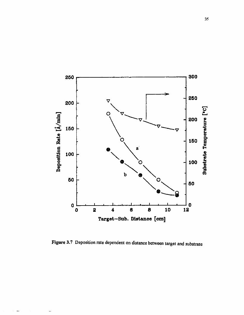
3.7 Deposition rate dependent on distance between target and substrate......................... 35
3.8 Deposition rate dependent on plasma current................................................................37
3.9 Deposition rate dependent on argon sputtering pressure...............................................38
3.10 Residual gas pressure with increasing argon gas pressure........................................... 40
3.11 Representative simulation of electron trajectories in magnetron sputtering............... 41
3.12 Simulation of argon ions trajectories after bombardment with electron..................... 44
3.13 Picture of erosion profile in target surface.................................................................... 45
4.1 Sputtering deposition of compound ceramic oxide films with different target formations.........................................................................................................................50
4.2 Multi-component metal target design for PLT film....................................................... 52
4.3 Capacitors with structure of (a) Pt/PLT/Pt-multilayer (Ti/SiC^/Si) substrateand (b) Pt/PLT/Pt-MgO substrate.................................................................................. 59
5.1 Relationship between the relative composition of sputtered PLT films andthe corresponding area ratio of multi-component metal target................................... 68
6.1 Dielectric constant and dissipation factor of PLT (28) thin films as a functionof post-annealing temperature........................................................................................ 77
6.2 Dielectric constant of 200 nm PLT (28) thin film with different temperature............. 79
6.3 Changes of the dielectric constant with increasing lanthanum (La)concentration of PLT films as described in Table 5.3.................................................... 81
6.4 Typical Sawyer-Tower circuit for polarization-electric field measurement.................83
6.5 Leakage current density as a function of annealing temperature for PLT filmsat 150 KV/cm (3 V)........................................................................................................ 86

LISTS OF FIGURE(Continued)
Figure Page
6,6 (a) Schematic test circuit with a peak voltage of unipolar pulse and a 1 Kfi load resistor, (b) The estimation of triangular area from transient response of I-t curve shows charge storage density..........................................................................89
A.l Auger electron spectroscopy spectrum of pure Pb....................................................... 98
A.2 Auger electron spectroscopy spectrum of pure La....................................................... 99
A.3 Auger electron spectroscopy spectrum of pure Ti...................................................... 100
A.4 Typical RBS spectrum of standard PLT film for semiquantitative AESanalysis............................................................................................................................ 101
A.5 Typical AES spectrum of standard PLT film ..............................................................102
A.6 Typical results of AES analysis on an as-deposited PLT film....................................103
A.7 AES spectrum of PLT (28) thin films with different target area:(a) Pb : La : Ti = 8.38 : 5.85 : 85.76(b) Pb : La : Ti = 7.60 : 7.80 : 84.60........................................................................... 104
A.8 Auger depth profile of an as-deposited PLT film as a function of etching time 106
A.9 Auger depth profile of PLT (28) films with different target area:(a) Pb : La : Ti = 8.38: 5.85: 85.76(b) Pb : La : Ti = 7.60 : 7.80 : 84.60........................................................................... 107
A. 10 Rutherford backscattering spectra of PLT thin films with different area ratioof multi-component metal target..................................................................................109
A .ll XRD patterns of PLT thin films with different post-annealing treatment.These PLT films belong to the type D in Table 5.3.................................................... 113
A. 12 XRD spectra of the paraelectric PLT (28) thin films as a function of postannealing temperature. These PLT films belong to the type A in Table 5.3............114
A.13 XRD step scans to observe the (211) peak shift of PLT (28) films at 550,650, and 750 °C for 5 m in............................................................................................115
xiv
LISTS OF FIGURE(Continued)
Figure Page
A.14 XRD patterns as a function of annealing temperature for PLT thin films ofchemical composition type B in Table 5 .3 ...................................................................116
A.15 XRD spectra of PLT thin films on single-crystal MgO (100) substrate................... 117
A.16 XRD patterns of the paraelectric PLT (28) thin films as a function ofannealing time at 650 °C............................................................................................... 118
A. 17 Typical SEM of as-deposited PLT film with smooth surface....................................119
A. 18 Typical SEM of PLT thin film annealed at 650 °C for 5 min.................................. 119
A.19 Segregation of grain boundary in PLT films due to Pb evaporation.........................120
A.20 SEM of typical defects on PLT films annealed at 750 °C for 60 min:(a) crack and (b) craters and holes.............................................................................121
B.l P-E characteristics as a function o f peak voltage for 200 nm PLT (28) thinfilm at 650 °C for 5 min................................................................................................. 122
B.2 P-E characteristics with different peak voltages for 200 nm PLT (28) thin filmat 750 °C for 5 min.........................................................................................................123
B.3 P-E characteristics as a function of annealing temperature for PLT films at thesame peak voltage of 4 V (200 KV/cm)....................................................................... 124
B.4 I-V plot of PLT thin films with different post-annealing temperature for 5 min 125
B.5 The phenomena of dc voltage-induced resistance degradation suddenly risingin the leakage current level prior to dielectric breakdown..........................................126
B.6 I-V characteristics for different delay time of a 5 sec using non-switchingstatic current...................................................................................................................127
B.7 Voltage-time characteristics of PLT (28) MDM capacitors with differentpeak voltage of unipolar pulse..................................................................................... 128
XV
LISTS OF FIGURE(Continued)
Figure Page
B.8 Switching time response characteristics as a function of load resistance underthe same peak voltage of 4 V (200 KV/cm)............................................................... 129
xvi

CHAPTER 1
INTRODUCTION
The ferroelectric elements in integrated semiconductor devices can be utilized in a variety
of ways based on the piezoelectric, pyroelectric, dielectric and electrooptic properties.
Compound ceramic oxides, which are well known as ferroelectric materials of PT family
systems, are PbTi03 (PT), Pb[Zr,Ti]03 (PZT), [Pb,La]Ti03 (PLT) and [Pb,La][Zr,Ti]03
(PLZT). Particularly, PLT films through a proper choice of lanthanum (La) content can
be used for various device applications, including piezoelectric sensors, dielectric devices
and electrooptic storage cells [1,2].
Ferroelectric thin films of PT systems with a high dielectric constant and low
leakage current density have received dramatic attention for the development o f memory
devices [3], Ferroelectric films, in the non-volatile random access memory (NVRAM)
application, use a large value of the remanent polarization in the hysteresis property of the
polarization versus electric field. In the dynamic random access memory (DRAM)
application, the high dielectric constant of ferroelectric materials can be exploited by using
a thin film capacitor as the charge storage element. On the La modified PbTi03 solid
solution system (Pb-La-Ti-0 system), PLT films with controllable composition and good
crystallinity are highly desirable due to the relevant dependence of the memory devices.
As the La content in the equilibrium phase diagram of the PLT system reaches 28 mol %,
the ferroelectric tetragonal structure of PLT thin films is suddenly transformed into a
paraelectric cubic phase. Paraelectric (non-ferroelectric) PLT films which offer good
dielectric properties and extremely low leakage current density are, therefore, an excellent
candidate for ULSI DRAM applications.
Several deposition methods have been used to synthesize ferroelectric ceramic thin
films, including magnetron sputtering [4,5,6], ion beam sputtering [7,8], MOCVD [9],
1

2
metalorganic decomposition (MOD)[ 10,11 ], sol-gel solution method [12,13], and excimer
laser ablation [14,15], etc.. Magnetron sputtering (dc or rf) of various deposition
techniques is the most popular growth processing for ceramic oxide materials, because the
desired composition of ferroelectric films is obtained easily from the compound target or a
multi-element metal target. Paraelectric PLT (28) thin films in our experiments are
prepared by reactive magnetron sputtering deposition using a multi-component metal
target. The deposited films experience the various conditions o f post-deposition annealing
for the desired perovskite structure and good crystallinity.
The present work is organized into five parts. The first part describes the
background and theory of ceramic oxide PLT material including the ferroelectric and
paraelectric (non- ferroelectric) structures. The second part introduces the operation and
advantages of a triode magnetron sputtering system, and explains the design and structure
of a magnetron sputtering system and its calibration tests. The third part presents the
preparation and experimental procedure of paraelectric PLT thin films. The PLT thin
films are deposited on Pt/Ti/Si02/Si or Pt/MgO substrate by reactive magnetron sputtering
using a multi-component metal target. The fabrication of ternary ceramic PLT thin films
includes several conditions of post-annealing treatment for the desired perovskite phase
with a high dielectric constant. The fourth part chiefly describes the material properties of
PLT thin films. Paraelectric PLT (28) thin films are characterized for stoichiometric
composition and cross-sectional profile by Rutherford back-scattering (RBS) and Auger
electron spectroscopy (AES). They are analyzed for surface morphology by scanning
electron microscopy (SEM), and evaluated for phase contents and crystallinity by X-Ray
diffractometry (XRD). The fifth part introduces the electrical properties of these films
which are analyzed by I-V plot, P-E measurement, V-t characteristics and dielectric
measurements.

CHAPTER 2
BACKGROUND OF PLT MATERIALS
2.1 Ferroelectric State
Since Busch and Scherrer in Switzerland discovered the ferroelectric properties in 1935
[16], there has been increasing interest in ferroelectric ceramic oxides such as PT systems
(namely, PT, PZT, PLT and PLZT). Ferroelectrics are a subgroup of the pyroelectric
materials, which are a subgroup of the piezoelectric materials. Ferroelectrics, therefore,
possess fundamentally both pyroelectric and piezoelectric properties, in addition to their
unique ferroelectric properties. Ferroelectric materials usually show hysteresis effects in
the relationship between dielectric displacement (or polarization) and electric field. A
ferroelectric oxide is characterized by a net spontaneous polarization (or electric dipole
moment) which can be switched or reoriented by the applied electric field. The
spontaneous polarization (Ps) has its origin in the noncentrosymmetric arrangement o f the
B-site ions (i.e., Ti) in the unit cell [17].
In ferroelectric materials, there are regions of aligned electric dipoles, called
domains, to produce the spontaneous polarization. The domains grow parallel to the field
as an electric field is applied, and the polarization is increased as shown in Figure 2.1. The
macroscopic polarization with an external field applied is composed of the aligned
spontaneous polarization as well as electronic and ionic polarization generated by the
external field. A maximum alignment of the spontaneous polarization occurs and the
hysteresis curve saturates at maximum polarization (Pm) because additional electronic and
ionic polarization produced by an increase in the field is quite small compared to the
spontaneous polarization. The ionic and electronic polarization decrease to zero when the
electric field is removed. The remanent polarization (Pr) is the spontaneous polarization
that remains aligned with the previously applied field. In the hysteresis characteristic, the
3
P (n
C/c
m2)
-Pmax
Ferroelectric
PrDielectric
-Ec
Ec
-PrQ'c
Pmax
E (kV/cm)
Figure 2.1 Typical polarization-electric field (P-E) characteristics for a ferroelectric and a dielectric.

5
magnitude of the reverse electric field, which decreases the net polarization to zero, is
called the coercive field Ec . At this point the net polarization reverses polarity if the
reverse applied field is increased further.
Ferroelectric PLT materials have a number of properties which make them useful
in a variety of application [18,19,20], for example,
(1) high piezoelectric constant
(2) high dielectric constant
(3) relatively low dissipation factor
(4) high electrical resistivity
(5) fairly high pyroelectric coefficient
(6) high optical transparency
(7) high electrooptic coefficient
Although all these properties do not simultaneously combine to produce an optimum
effect in any application, a number of desirable properties can be achieved by adjustable
control of the La content in PLT thin films.
The perovskite structure in the ferroelectric phase of PLT oxide material assumes
one of three structural formations: tetragonal, orthorhomic, or rhombohedral. The PLT
solid solution system is a series of compositions modified by the solubility of substantial
amounts of lanthanum oxide (La20 3) in the crystalline lattice of lead titanate (PbTi03).
PLT material possesses the perovskite crystal structure described by the general chemical
formula AB03 [19] as shown in Figure 2.2. The A element (Pb and La) is a large cation
situated at the comers of the unit cell and the B element (Ti) is a smaller cation located at
the body center. The oxygen atoms are positioned at the face centers. The chemical
formula of the PLT system [21,22] can be generally expressed in two forms depending on
the type of vacancies:
(A) Pbj.xLajTij.j/^Oj
(B) P b ,^xLaxT i03

6
Figure 2.2 Unit cell of Pb-La-Ti-0 system as a perovskite ABO3 ciystal structure

7
where a is called the vacancy distribution factor (or lead elimination factor) in the range
0.75 < a < 1.5, and essentially depends upon the partial pressure of the PbO, the amount
o f lanthanum (La), substrate temperature, and the partial pressure o f oxygen [23], In
these formula, La ions replace Pb ions in the A-site of the perovskite AB03 ionic
structure. Since La3+ (added as La20 3) substitutes for Pb2+, electrical neutrality is
maintained by the creation of lattice site vacancies. The actual location of these vacancies
in either the A2+ sites or B4+ sites of the unit cell has not yet been completely reported
despite numerous studies on the subject [19-23], It is most probable that vacancies exist
in both A- and B-site [21]. If both A- and B-site vacancies are present in the lattice, it is
expected that the above formulation would provide excess Pb2+ ions which are expelled
from the lattice (PbO vapor) during the annealing process. In fact, this excess PbO
contributes to achieving full dense material by eliminating residual porosity before it
becomes entrapped within the grains. Lead titanate (PbTi03) is a tetragonal ferroelectric
perovskite material with the Curie temperature (Tc) o f490 °C, and its tetragonality, c/a, is
1,06 at room temperature. The addition of La to the bulk ferroelectric PbTi03 causes a
unit cell contraction [24], The c/a ratio and Tc decrease monotonically with increasing La
concentration. Therefore, the effect of adding La of the PT system is to reduce the
stability o f the ferroelectric phases (reducing the Curie temperature) in favor o f the
paraelectric (non-ferroelectric) cubic phase.
The composition-structure relationship in the equilibrium phase diagram for the
PLT system [23,25] at 1330 °C is given in Figure 2.3. Since the phase diagram in the
Figure is applied only to films that form during deposition, it can not be directly formalized
in PLT thin film using post-annealing treatment. Fox et al [26] discussed in detail that
PLT films heat-treated by post-deposition annealing were evolved from the interdependent
relationship between stoichiometric composition and crystallographic structure. A post
deposition annealing process is required for films deposited in the amorphous or partially
amorphous state. The annealing parameters, that is, temperature, time and oxygen partial

Tetrag. perovskite Cubic perovskite Perovskite + PbO Perovskite+ LO2Ti20
cub. perov.
tetr. perov.
0.6 PbTiO, 0.4 0.20.3 0.1— PbO
Figure 2.3 Equilibrium phase diagram for the PLT system at 1330 °C
9
pressure, have prominent influences upon crystallization and perovskite phase formation in
PLT films [3], Surface microstructures of the deposited thin film have commonly been
introduced by the structure zone model (SZM) [27], as shown in Figure 2.4.
Microstructures and morphologies of the thin film are classified by the deposition
temperature and argon operating pressure. There are three microstructure zones in the
SZM. Zone I (T/Tm < 0.25 - 0.3) is a porous structure consisting of tapered crystallites
separated by voids. Zone II (0.25 - 0.3 < T/Tm < 0.45) has columns with relatively
smooth surfaces. Zone III (T/Tm > 0.45) shows the recrystallized grain structure. The
transition zone (subzone T) at the border between zone I and zone II exhibits a tightly
packed fibrous structure. The post-annealed films are different from the microstructure of
as-deposited films because of thermally induced surface and bulk diffusion. It is supposed
that the final microstructure of PLT thin films using the post-deposition annealing is
exhibited by a superposition of various zone structures in the SZM model due to the
interdependent processes of crystallization and composition change caused by lead
volatility.
2.2 Paraelectric State
There are two ways to perceive the paraelectric state in the Pb-La-Ti-0 system. First, as
the molar La content in the composition formula of the PLT system is equal to and higher
than 0.28, the paraelectric phase with cubic perovskite structure appears in the PLT phase
diagram as given in Figure 2.3. It is noted that its tetragonality (c/a) is unity and the Curie
temperature is -25 °C [28]. Second, the ferroelectric behavior of PLT thin films
disappears at a specific transition temperature with increasing temperature. The
spontaneous polarization in ferroelectric film is a function of temperature. However, at
high temperature, thermal energy destroys the domain structure of ferroelectricity. The
specific temperature at which the spontaneous polarization disappears is called the
ferroelectric Curie temperature. Above the Curie point (Tc), PLT material is suddenly

10
CAze£«DC<Z
§
W w : V :-">
UJ 01Uujt-
Ui UJo o
Figu
re
2.4
Thin
film
struc
ture
zo
ne
mod
el (S
ZM)
defin
ed
by T/
Tm and
the
en
ergy
of
depo
sitin
g sp
ecie
s

11
changed from ferroelectric (or noncentrosymmetric) tetragonal phase to paraelectric (or
centrosymmetric) cubic state in the perovskite structure. As shown in Figure 2.5 (a), the
ferroelectric state (i.e., spontaneous polarization) exists at a temperature below Tc , and
also the spontaneous polarization equals zero above Tc .
The dielectric constant is not only a function of the electric field, but also a
function of temperature. Figure 2.5 (b) shows the dielectric constant as a function of
temperature. In the ferroelectric phase, the dielectric constant increases gradually as the
temperature increases, and it becomes anomalously large at the Curie temperature. Above
Tc, the dielectric constant can be frequently described by Curie-Weiss behavior:
1 _ T - T c e ~ C
where, C is the Curie constant and
Tc is Curie temperature.
The dielectric constant, as a function of temperature, in the paraelectric phase of the PLT
films can not be completely represented by the simple formula o f Curie-Weiss behavior.
Keizer et al [29] have developed models to interpret the anomalous dielectric
characteristics. The dependence of the dielectric constant on temperature for the
paraelectric phase of PLT (28) thin films can be modified by the power series of the
temperature as the following:
= c , - c ! ( 7 - - 7 ' „ ) - c J( 7 - - r ^ , ) iS B°m a x
where, Cj, C2 and C3 are constants, depending on the stoichiometric composition.
Dey and Lee [30] discussed that the ferroelectric thin films with hysteresis effect
exhibited a number of disadvantages for semiconductor memory applications. The time-

12
Ps
ParaFerro
TTc
(a)
8
Ferro Para
Tc T
(b)
Figure 2.5 The dependence of (a) spontaneous polarization and (b) relative dielectric constant on temperature (near Curie temperature).

13
dependent polarization reversal processes in the saturation arm between Pr and Pm of a
hysteresis loop are relatively slow. This processes, in terms of domain reorientation and
phase switching, produce a potential fatigue (time-dependent degradation in charge
storage density) and severely limit the charging and discharging speeds of the capacitors.
Therefore, nonswitching cubic paraelectric films with high dielectric constant should offer
outstanding advantages over switching ferroelectrics.
Figure 2.6 shows polarization versus electric field (or called P-E) characteristics
for normal dielectric, paraelectric, and ferroelectric thin films. The typical P-E
characteristic of a ferroelectric film exhibits the hysteresis loop with the positive and
negative remanent polarization values. Conversely, paraelectric PLT film behaves like a
normal dielectric material at a low electric field, and has no remanent polarization in the
absence of an electric field. At a high electric field, the nonlinear behavior is demonstrated
in paraelectric films. The dielectric and electrooptic effects o f ternary ceramic PLT thin
films are greatly affected by the La content, and they reach maximum effect near the phase
boundary (Jt = 0.28) between the ferroelectric tetragonal and the paraelectric cubic
structure [22],
2.3 Potentials of PLT Material for DRAM Capacitor
With the successful development of dynamic random access memory (DRAM)
technology, the reduction in cell size has required reducing the area of the planar storage
capacitor. It is, therefore, necessary to increase the charge storage density on the
capacitor to maintain adequate operation. The required increase in charge storage density
has been achieved through improvements in processing technology, reduction of the
dielectric thickness, and innovations in the cell design (31]. However, the thin dielectric
materials such as conventional dielectrics as well as Ta20 5 and Si3N4/Si02 do not appear
to be sufficient for ultra large scale integration (ULSI) DRAMs. As a result, a new

14
para
elec
tric,
and
(c)
hys
tere
sis l
oop
for f
erro
elec
tric.

15
dielectric material that permits a capacitor with higher charge storage per unit area and is
compatible with ULSI processing is required for use in ULSI DRAMs.
Ferroelectric materials as an alternative dielectric with a higher dielectric constant
have been widely considered by a large of number of researchers [31,32], There are
numerous important requirements that have to be satisfied by the dielectric material for
future generations of DRAMs and they are as follows:
( 1) high charge storage capacity per unit area,
(2) low leakage current density,
(3) low defect density,
(4) high reliability,
(5) compatibility with silicon integrated circuit processing technology, and
(6) stability with the two capacitor electrodes.
Table 2.1 shows key parameters required for the electrical properties of recent ULSI
DRAMs.
Table 2.1 Key parameters required for the electrical properties of 64 and 256 Mb DRAMs.
Parameter 64 Mb 256 Mb Comment
Memory cell area (pm^)
0.7-1.0 0.25-0.34 —
Storage capacitor 2-6 0.7-2 Trencharea (pm^) 0.2-0.5 0.07-0.17 Planar
Storage charge 1-5 2-11 Trenchdensity (pC/cm^) 10-50 20-115 Planar
Leakage current 2-25 3-35 Trenchdensity (pA/cm^) 20-250 30-360 Planar
Dielectric thickness (nm)
10-200 10-200 —

16
A DRAM memory circuit uses charge storage on a capacitor to represent binary
data values. The most common DRAM memory cells are based on the one-transistor (1-
T) design to reduce the size of DRAM. This has the advantages of a small memory cell
area made possible by the use o f only one transistor and one storage capacitor in the
circuit design. The 1 -T cell is also comparatively easy to fabricate, operates at less power,
and is more reliable than other designs using multiple transistors. Figure 2.7 (a) shows a
typical memory cell with a single transistor and capacitor for charge storage. The 1-T cell
of the basic DRAM technology was invented by Dennard [33], Its concept is that the "0"
and "1" binary information is stored on the capacitor by charging or discharging the
capacitor through the transistor. The transistor connected to the word line isolates the
storage capacitor from the bit line, and as soon as the transistor is turned on, the capacitor
is connected to the bit line so that information is written and read. A cross-sectional
structure of 1-T DRAM cell [34,35] with a paraelectric capacitor is shown in Figure 2.7
(b). Similar to the conventional I-T memory cell, the single transistor as a pass transistor
provides a path to the capacitor. During operation, a positive or zero voltage is on the bit
line for the "1" or "0" state, respectively. However, the critical factor in the design of a 1-
T DRAM cell is the charge storage density which fundamentally determines the
effectiveness of the memory cell to maintain the distinction between "0" state and "1"
state.
Recent researchers [36,37] suggest that the improvement in the relative dielectric
constant using a thin insulating material such as tantalum pentaoxide (Ta20 5; 8r ~ 20-25)
and yttrium oxide (Y20 3; Er ~ 12-16) is 3 to 6 times over that o f Si02, while the net gain
in charge storage density is only a factor of two at best. This is due to higher leakage
current and lower dielectric breakdown strength. The requirement for high charge storage
capacity per unit area is focused on dielectric material with an extremely high dielectric
constant. The ability of the dielectric constant with the use of new dielectrics can

17
Bitline
1
I
Word line
__— Transistor gate
Storage capacitor
(a)
Metal • Top electrode
Paraelectric
Bottom electrode
Silicon substrate
(b)
Figure 2.7 (a) Circuit elements of one-transistor (1-T) DRAM cell, and (b) Cross-sectional structure of 1-T cell involving paraelectric capacitor.

18
withstand a sufficiently large electric field, because the charge storage capacity is
proportional to the dielectric constant and the applied electric field.
In recent reports for DRAM operation [38], a PZT film of 400 nm thick is
equivalent to a 1.6 nm Si02 film subjected to a 2.5 V voltage (5.5 pC/cm2). The 200 nm
film has a polarization of 9 pC/cm2 equivalent to a 1.0 nm Si02 film with a 2.5 V voltage.
Paraelectric PLT (28) films of 500 nm thick have a polarization of 5.7 pC/cm2 with a 2 V
voltage. The largest charge storage capacities reported for ONO (oxide/nitride/oxide) and
Ta20 5 dielectrics correspond to a 2.5 nm Si02 film. The film thickness of the dielectric
has been reduced to less than 10 nm in order to retain a sufficient charge storage in current
DRAM technologies. A further reduction in thickness may have a deleterious impact such
as a direct tunneling through thin dielectric films and has reached the fundamental limit in
processing technology.
Another important capacitor dielectric requirement for any potential DRAM is low
leakage current density. High leakage current has limitation in the operation since the
cells require more frequent refreshing, use more power, and limit the maximum field that
may be applied across the device. Figure 2.8 shows the leakage current density as a
function of the electric field for the various dielectric materials [39,40], The PZT and PLT
films exhibit superior leakage characteristics compared to other dielectric films at high
fields.
Charge storage density, in ferroelectric thin film, corresponds to the difference
between the maximum polarization and the remanent polarization in hysteresis loop. The
ferroelectric PZT films for DRAM operation present some disadvantages such as time
dependent polarization reversal processes in the saturation of the hysteresis loop. These
processes not only cause a potential fatigue (time-dependent degradation of Qc) problem
but can also increase loss tangent and seriously limit the switching speed of the capacitors.
The hysteresis property is not actually desirable in DRAM application, and the capacitor
operates only as a linear capacitor. Therefore, paraelectric cubic PLT films with extremely

19
e"7 TO I °f©
Eo
2"3tco•c
•4—ioVW
[jUio/v] Ajisuap tuaxino 38BJjBaq
Figu
re
2.8
Com
paris
on
of lea
kage
cu
rrent
den
sity
of PL
T thi
n film
wi
th ot
her
diel
ectri
c m
ater
ials.
PL
T film
sh
ows
supe
rior
char
acte
ristic
to
othe
r D
RA
M
diel
ectri
c

20
high dielectric constant and normal dielectric characteristics should offer significant
advantages over ferroelectric films.
Charge storage densities, leakage current densities, and dielectric thickness in
recent ULSI DRAM technologies with planar capacitor are basically required to be in the
range of 20-115 pC/cm2, 30-36 pA/cm2, and 0.01-0.2 pm, respectively [41],
Paraelectric PLT thin films are a potentially attractive candidate for the storage dielectric
capacitor in future DRAMs. Nonswitching cubic paraelectric PLT thin films with a linear
dielectric characteristic offer significant advantages over conventional dielectrics and are
also preferable to nonlinear switching ferroelectric thin films for the operation of ULSI
DRAMs.
2.4 Objectives of Research
Ferroelectric thin films have been developed in semiconductor memories that are
optimized for a variety of applications. These are static random access memories
(SRAMs) that are required for high speed applications; dynamic RAMs (DRAMs) that are
designed for computer storage; and nonvolatile RAMs (NVRAMs) that are used for read-
only-memory. The important characteristics of ferroelectric materials are specified by
special properties for all types of memory devices of the memory application as follows.
Nonvolatile ferroelectric memories utilize a ferroelectric thin film capacitor as a
nonvolatile storage element and make use o f the hysteresis property of polarization versus
voltage characteristics. The high dielectric constant o f ferroelectric materials can be
exploited by a thin film capacitor as the storage element in DRAM devices. Here, the
hysteresis property of ferroelectric is not desirable, and the capacitor operates similar to a
linear capacitor of normal dielectric for charge storage. Consequently, the paraelectric
PLT (28) thin films with excellent dielectric properties are expected to offer significant
advantages for ULSI DRAM technology.

21
Many researchers have used various deposition techniques for preparation of
ferroelectric oxide thin films. Adachi et al [42] succeeded in the epitaxial PLZT thin films
on sapphire and MgO substrates by rf magnetron sputtering method from an oxide powder
target. Schwartz et al [43] prepared ferroelectric PLT thin films by the sol-gel solution
method. Watanabe et al [44] fabricated amorphous PLT (15) thin films by metal organic
chemical vapor deposition (MOCVD) at low temperature. Quin et al [45] and Fox et al
[46] also made ferroelectric PLT thin films by a multi-ion-beam reactive co-sputtering
technique. The common interests in preparing PLT thin films of high quality by different
deposition methods include stoichiometry control, suitable microstructure, uniformity,
reproducibility, and process compatibility with semiconductor technology.
To date, preparation of PLT thin films with correct composition is so difficult that
their electrical properties for memoiy device technologies have not been investigated
sufficiently. Thus, this study begins with a development of high dielectric properties in
ferroelectric oxide materials for ULSI DRAM application. The first purpose of the
present research work is to prepare paraelectric PLT thin films by a multi-component
metal target of triode magnetron sputtering technique which is designed in our laboratory.
Subsequently, a post-deposition annealing treatment for the as-deposited films is carried
out to crystallize into the desired perovskite phase. The material and electrical
characteristics of the films are also investigated by a variety of analytic methods. RBS and
AES are used in order to achieve the desired stoichiometric composition of PLT (28) thin
films. XRD is also used to determine the crystalline structure and lattice constant of PLT
thin films. The surface microstructure is analyzed by SEM topography. The dielectric and
electrical characteristics such as P-E, I-V and V-t measurements are investigated to
illustrate the potential use of PLT (28) thin films in DRAM application.

CHAPTER 3
TRIODE MAGNETRON SPUTTERING SYSTEM
3.1 Introduction
Presently, the most important factor in the preparation of ferroelectric oxide films is the
deposition method. In the ferroelectric thin film (FTF) growth processes, Krupanidhi [47]
reported that the deposition techniques could be primarily specified in terms of the growth
processes with and without the presence of low energy bombardment during deposition.
The growth processes with low energy bombardment included, magnetron sputtering, ion
beam sputtering, excimer laser ablation, electron cyclotron resonance plasma-assisted
growth, and plasma-enhanced chemical vapor deposition (PECVD). The deposition
techniques without bombardment included sol-gel synthesis, metalorganic decomposition
(MOD), thermal and e-beam evaporation, CVD, MOCVD, and MBE. Table 3.1
summarizes the various growth techniques for recent FTF processing o f PT systems [47],
Sol-gel processing in chemical solution methods and magnetron sputtering of the
above mentioned methods have been reported as successful preparation techniques
because of better control of the film composition. The sol-gel technique has received
significant attention due to easier fabrication of a large area, excellent lateral uniformity
and low cost. However, sol-gel deposition has a number of disadvantages such as the
inability of exact thickness control for thin films and difficulty of small feature deposition.
Due to the recent requirements for ultra large scale integration (ULSI) o f ferroelectric
oxide/semiconductor thin film-based devices, rf or dc magnetron sputtering of physical
deposition techniques have received dramatic attention [18,47], The multi-component
target sputtering, or multiple targets sputtering, appears to be a suitable method to deposit
stoichiometric thin films with controllable thickness and high growth rate.
This chapter briefly introduces the theoretical background and construction of
22

23
co•a09r a
-D
Etcc
1c
utuot,4i
V) ■*-<D C 3 43cr £
'5 ’Sr* V-o _g 43*- ES ° o x>C t*-onO „Q. ua>•a093O•E03>r*t<us03H
e<u09Vu.Q.<U UJ _ J
E o>
n *C a) v at e c a £ </)
LL
li.
H N a . cl
Na .
a. a. a.
t— I—I - N - I CL CL a . CL
H0.
cl cl a .
CL CL
» - N CL CL CL CL

24
triode magnetron sputtering which was designed in our laboratory, and the basic tests for
its calibration. Finally, the ternary ceramic oxide of PLT thin film with a high dielectric
constant and a low leakage current is deposited reactively by our triode magnetron
sputtering.
3.2 Triode Magnetron Sputtering
3.2.1 Magnetron Sputtering
Sputtering is an atom-by-atom process. Atoms are ejected from the surface of a target
under ion bombardment and subsequently deposit to the substrate. Sputtering as a
phenomenon was first observed to coat mirrors in the 1850s [48], In the 1940s, sputtering
was used to a significant extent as a commercial deposition process. A typical magnetron
sputtering process shown in Figure 3.1 has a shaped and closed path magnetic field to trap
and concentrate the electrons produced in the discharge at the target surface. The
electrons are confined to above the target materials. The high density cloud of electrons
promotes ionization of the sputtering gas in the region close to the target surface, and the
target is negatively biased to attract ions to the target. The high energy impact of these
ions on the target dislodges atoms from the material which are collected on the substrate
surface. Due to the high ionization efficiency of this process, low power levels may be
used, and at the same time high deposition rates are achieved. Because electron leakage is
restricted by the magnetic field, bombardment of the substrate is minimized and heating of
the growth film and substrate is substantially reduced.
The magnetron sputtering process has many advantages [48,49], The primary
advantages are:
(1) high deposition rate,
(2) ease of sputtering any metal, alloy, or compound,
(3) high-purity of the deposited films,

25
"E" Field
Material Removedby Ion Bombardment "B" Field
GrowingFilm
7
\ O
Target with Negative High Voltage
CapturedElectrons
Magnetic Field Lines
O Target Atoms 0 Ionso Argon Atoms • Electrons
Figure 3.1 Basic operation of magnetron sputtering system

26
(4) extremely high adhesion of films,
(5) excellent coverage of steps and small features,
(6) ability to coat heat sensitive substrates,
(7) ease of automation, and
(8) excellent uniformity on large area substrates.
Magnetron sputtering, because of the above advantages, is a very powerful technique
which can be used in a wide range of applications.
The advantages of a triode technique in a triode magnetron sputtering are that a
very high ion density is produced, the processing pressure is relatively low and the plasma
current density for the deposition films can be controlled independently with the plasma
voltage. Therefore, the deposition rate of triode magnetron sputtering is higher than that
o f diode magnetron sputtering. There are also some disadvantages in terms o f the heated
filament. First, the thermionic filament is impractical in the reactive sputtering process.
Second, the filament of the refractory metal contributes to contaminate the deposited
films. The filament is subject to burnout and its power dissipation adds heat to the
chamber area.
3.2.2 Construction of Triode Magnetron Sputtering System
Figure 3.2 shows a frontal picture of a triode magnetron sputtering system, including the
vacuum chamber, power supply, and system control console. The block diagram of the
sputtering system is shown in Figure 3.3. In this section, the triode magnetron sputtering
system is discussed in terms of its structure and the details of its construction. A
generalized magnetron sputtering system consists of a high vacuum system, a sputtering
source assembly, and a substrate holder in its basic formation. The design and
characterization of a triode magnetron sputtering system will be presented.
The vacuum system used for this triode magnetron sputtering system was
previously an asymmetrical reaction ion etch system, model 640, built by Plasma-Therm,
Tabl
e 3.2
Pa
rtial
pre
ssur
e in
the
sput
terin
g ch
ambe
r be
fore
intro
ducin
g the
arg
on
gas
27
( D C D N O O O I O I O O O O O O
I I I I I I I I I I I I L U L U L l I I j J I J L I L U I ± J L l I I i J L U L i J 1 U ^ Q N . O I I M Q Q Q Q Q Q Q m vi OD 'sf CD ^
c o n m o i r n N o o o o o o' H ^ r m - c u i n ^ o o o o o o^ ( f l Q Q O l Q Q Q Q Q Q(\| f \ v l v l -H tH tH v t tH t -| v t
ZLjJ 00 1 U ZO D I UJ ZI H | U \ 0 O O O O O O O □ J I- > 0> u j < ai x tr1 1 2 Z 0 <r I
NF
IC
ON
Q
UA
DR
EX
2
00

28
Figu
re
3.2
Fron
t pic
ture
of
triod
e m
agne
tron
sput
terin
g

29
Inc [50], The dimension of bell jar chamber is 32-inches high by 24-inches outer diameter.
The vacuum system consists of a turbomolecular pump, rough and process mechanical
pump. A residual gas analyzer (Leybold-Heraeus, Inficon, Quadrex 200) is attached to a
flange between the base of the bell jar and the turbomolecular pump. It is used to monitor
vacuum chamber performance, such as, various residual gases, and to detect vacuum leaks
and contaminants. The lowest base pressure observed in the vacuum chamber has been
2.5x1 O'6 Torr. The partial pressures of residual gases in the vacuum chamber is shown in
Table 3.2.
The target source assembly is a TRI-MAG, model 383, sputtering source by
L.M.Simard, Inc., and TRI-MAG stands for triode and magnetron sputtering system.
This sputtering source has an exceedingly high deposition rate for thin film research. In
the triode system, ions are generated in low voltage (50-70 V) and high current (2-15 A)
arc discharge between a thermionic filament (tantalum) and a main anode. The magnetic
field design is the key factor governing the operation of the magnetron in the planar
magnetron system. It is responsible for the effective trapping of the electrons and the
uniform erosion of the target material. Unique characteristics of thin film deposition is
given by an ExB field for plasma confinement close to the target surface. The magnetic
structure under ExB field is configured to give exceptionally uniform target erosion and to
permit the sputtering of insulators as well as magnetic materials. The source of the
permanent magnets for the magnetron system is a ferrite, so called "ceramic 8", and its
magnetic flux strength is around 250 Gauss [51]. Figure 3.4 shows the entire sputtering
source assembly, including the water lines and the electrical connections, based on the
above essential limitations. The power block diagram of the triode magnetron sputtering
source is given in Figure 3.5. The substrate holder is located above the sputtering source
assembly so that the deposited thin films have a high purity due to the sputtering-up
position. The substrate holder is made of a 4 inch diameter copper disk.

30
CONTROLS MASS ROW PROCESS GAS 2 ROTOMETER
PROCESS CAS ROW CONTROL
I______ -A______ J
Figure 3.3 Block diagram of triode magnetron sputtering

31
TAPQtr iioci A«at.
w* ' t itc n
I ® &
1 ’• I 8dflrj [|:Hc e « » * c T o »
( T * « o c r # o w t * f
C O A tU tV » U l« N * A OcoHMCcroM toe eoM««cfiOMi
vV WW'^ x W
b m v i p cart*
Figure 3.4 Entire sputtering source assembly

32
ANODE FILAMENT GAS INLET
HOUSING
TARGET MODULE (DC or RF)
_L +
i
AUTOIGNITIONMODULE
PLASMADISCHARGE
MODULE
FILAMENT
MODULE
PD/200POWER SUPPLY
Figure 3.5 Power block diagram of triode magnetron sputtering source.

33
3.3 Calibrating Tests of Triode Magnetron Sputtering
In order to calibrate the rf triode magnetron sputtering system for thin film deposition
processes, the effects of different glow discharge conditions were investigated in terms of
the deposition rate measurements. The basic parameters for calibrating experiment in our
rf triode magnetron sputtering were rf power input, gas pressure, plasma current, and
target to substrate distance. Because a knowledge of the deposition rate is necessary to
control film thickness and to evaluate optimal conditions which are an important
consideration in preparing better thin films, the deposition rates of copper as a testing
material under the various sputtering conditions were investigated.
3.3.1 RF Power Effect
The deposition rates dependent on the rf power are shown in Figure 3.6, and the
deposition rates increase linearly with increasing rf power input. The sputtering conditions
were: 70 mm distance between target and substrate, 20 mTorr argon gas pressure, 5 A
plasma current, and 60 minutes deposition time. In this Figure, the curve "a" shows the
deposition rate of a sample in the center location "1" on the substrate holder. The curve
"b" demonstrates the average value of deposition rates at four positions "2", "3", "4", and
"5" whose distance from the substrate center is 25 mm, respectively. Each deposition rate
on location "2", "3", "4", and ”5" was with maximum 5 % range o f the average value on
the curve "b". The temperatures of the substrate holder caused by ion bombardments of
sputtered atoms and thermionic filament in a triode system also increase with increasing rf
power. It is expected that the linear increasing curve of substrate temperatures occurs
mainly by ion bombardment with increasing rf power, because the plasma current causing
the thermionic filament is a fixed parameter during the growing processes.
3.3.2 Target to Substrate Distance Effect
Figure 3.7 shows the effect of distance between the target and substrate in the deposition

Depo
sitio
n Ha
te [A
/min
]
34
300250
250 t?200
200 I150
150 £
100
100 £
5050
20050 100 1500 250
RF Power Input [W]
Figure 3.6 Deposition rate dependent on rf power input (a) deposition rateof the center "1" on the substrate holder, and (b) average of deposition rate o f at four positions "2", "3", "4" and "5" with distance of 25 mm from the center
Rat
e
35
300250
250200
200
150
150
gS3 100*63o0 4©
Q100
50 A 50
128 104 62
Target—Sub. Distance [cm]
Figure 3.7 Deposition rate dependent on distance between target and substrate
Subs
trate
Te
mpe
ratu
re
[8C]

36
rate curve. The deposition rates as shown in this Figure decrease with the increasing
target to substrate distance. This means that the deposition rates are inversely
proportional to the transit distance of copper atoms, and the probability o f deposition on
the substrate gradually becomes low with increasing transit distance. The measurements
of substrate temperature is similar to the curve of the deposition rates under the same
sputtering conditions.
3.3.3 Plasma Current Effect
The advantages of a triode system is that a high ion density is produced and the plasma
current density for the deposition films can be controlled independently with the plasma
voltage. Figure 3.8 shows the deposition rates as a function of the plasma current. The
sputtering conditions were: 70 mm distance between target and substrate, 20 mTorr argon
gas pressure, 100 W rf power input, and 60 V plasma voltage. The deposition rates
increase linearly with increasing plasma current. As the plasma current is gradually
increased, electrons caused by a thermionically heated filament are increased. These
electrons accelerate toward the main anode where they then ionize a large portion of
argon gas molecules. The process occurring in the triode system relies on the abundance
of electrons generated by the thermionic filament to ensure sufficient ionizing collisions.
Thus, the ion population at the target surface is increased with increasing electrons, and
the deposition rates increase. The surface temperatures on the substrate holder depend
effectively on the plasma current in the triode system and this is shown in this Figure. The
curve of the substrate temperature increases with increasing plasma current, and it is
expected that the increasing temperature on the substrate is caused by the sputtering
deposition and by the thermionically heated filament.
3.3.4 Argon Sputtering Pressure Effect
Figure 3.9 shows the deposition rates with the different sputtering pressure of argon gas at

Depo
sitio
n Ra
te [A
/Min
]
37
200
V -
150
100 O “
50
52 3 74 6 80 1
300
- 250
200
150
100
50
Plasma Current [A]
Figure 3.8 Deposition rate dependent on plasma current
Subs
trate
Te
mpe
ratu
re
[°C]

Depo
sitio
n Ra
te [A
/min
]
140
120
100
20
0 10 20 30 40 50 60 70 80At Gas Pressure [mTorr]
Figure 3.9 Deposition rate dependent on argon sputtering pressure
39
70 mm distance between target and substrate, and 125 W rf power input. As the
sputtering pressure of argon gas is increased, the deposition rates decrease due to the
scattering between the argon gas and the sputtering particles. The mean free path
conspicuously decreases at higher sputtering pressures. Thus, the probability of collision
between argon atoms and sputtering atoms increases with a higher argon sputtering
pressure, and the probability of a sputtering atom reaching the substrate without colliding
with an argon atom is reduced.
Figure 3.10 shows the residual gas with the variance of the argon sputtering
pressure after 60 minutes from the starting of the sputtering deposition process. The
sputtering conditions are same with the Figure 3.9. Mass 18 is the water (H20 ) peak. 20
and 40 AMU in mass axis are Ar++ and Ar+ ions, respectively. As shown in this Figure,
the peaks of Ar++ and Ar+ ions increase absolutely at a higher Ar sputtering pressure.
Conversely, the water peaks keep almost constant with a rising sputtering pressure.
3.4 Simulation of Magnetron Sputtering System
A triode magnetron sputtering system which was designed in our laboratory was simulated
by the SIMION program [52], and the simulation of electron trajectories in the sputtering
system is given in Figure 3.11. The two dimensional structure of the sputtering source
assembly in the triode magnetron sputtering system was reduced by half scale to the actual
system. The magnetic flux strength of the system was 250 Gauss. The potential of the
main anode was a positive 50 voltages, and the substrate holder and housing of the target
assembly were grounded. It was assumed that Ar gas was not introduced into the
chamber in order to analyze the electron trajectories toward the main anode without
collision. The electron trajectories in the sputtering system are confined directly above the
target surface, as shown in this Figure. It shows that the electrons are trapped to the
target surface by the force of the ExB field as shown in Figure 3.1. An electron, emitted
from the filament, travels toward the main anode with the helical path. High electron

40
I I I I I M I I I I I « (U 0 0 (0 V W 0
< I Q . J H h D D Q J
I M I I CD CD ^r) rl ri
Figu
re
3.10
Resid
ual
gas
pres
sure
wi
th in
crea
sing
argon
ga
s pr
essu
re

Subs
trat
e
41
W E-1 ) CO
Figu
re
3.11
Repr
esen
tativ
e sim
ulati
on
of ele
ctron
tra
ject
orie
s in
mag
netro
n sp
utte
ring.
42
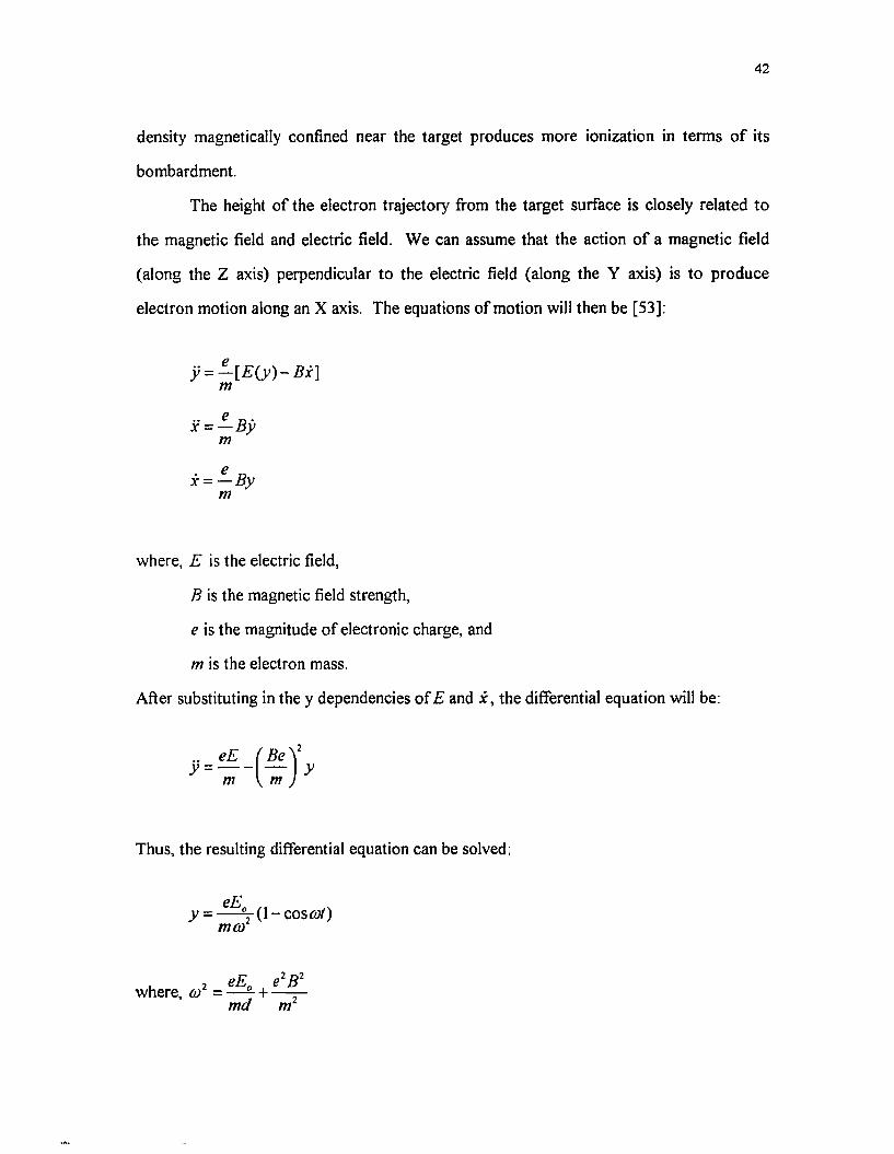
density magnetically confined near the target produces more ionization in terms of its
bombardment.
The height of the electron trajectory from the target surface is closely related to
the magnetic field and electric field. We can assume that the action of a magnetic field
(along the Z axis) perpendicular to the electric field (along the Y axis) is to produce
electron motion along an X axis. The equations of motion will then be [53]:
where, E is the electric field,
B is the magnetic field strength,
e is the magnitude of electronic charge, and
m is the electron mass.
After substituting in the y dependencies of E and x, the differential equation will be:
y = - [ E ( y ) - B x ] m
m
x = — Bym
Thus, the resulting differential equation can be solved:
2 eEa e2B2 where, (o - — - + — — md m

43
and d is the thickness of dark space. In the absence of the electrical field, a> is equal to
eB/m. This is known as the cyclotron frequency [53], It is noted that the traveling height
of an electron is also related to the thickness of dark space from this solution of the above
equation. The maximum height, ymax> ° f the electron from the target surface, assuming
no collisions, can be found by considering the gains and losses of potential and kinetic
energy [54]:
where, VT is the negative target voltage and F is the potential at y max. Since x = Bey Im,
then y max can be obtained:
y max2m (V -V T)
1/2
This expression holds both within and without the dark space, and is a better
approximation at lower pressures.
Figure 3.12 shows the trajectories of argon ions with the changes of their location
after bombardment by electrons. The sputtering conditions are same with the procedure
of Figure 3.11, and the target potential is a negative 200 voltages. Argon trajectories are
concentrated largely upon the center of the target surface and slightly closer to the
filament. The erosion profile of the target surface caused by Ar ion bombardment is
shown in Figure 3.13, and thoroughly corresponds with the results of simulation that
shows the collision of Ar trajectories. This erosion shape is mainly dependent on magnetic
field strength, magnetic field shape and target material, and is controlled primarily by the
magnetron design. It is known that the position and shape of this erosion directly affects
the thickness distribution of deposited film on the substrate. Therefore, the geometry of

Figu
re
3.12
Sim
ulati
on
of arg
on
ions
traje
ctor
ies
after
bom
bard
men
t wi
th el
ectro
n

45
Figu
re
3.13
Pictu
re
of er
osio
n pr
ofile
in
targ
et s
urfa
ce

46
the magnetron source is an important parameter for a magnetron sputtering system.
3.5 Discussion
The results of calibration tests with four different sputtering conditions demonstrates that
the deposition rate of rf triode magnetron sputtering is relatively higher than that of the
conventional sputtering system. This means that the higher deposition rate is probably
caused by a high ion density in the triode and magnetron system. The surface
temperatures, in the substrate holder, are particularly increased with increasing plasma
current in a triode system. It is evident that the results of electron and Ar ion trajectories
simulated by the SIMION program correspond well with the actual processes of triode
magnetron sputtering and the erosion profile of the target surface. The erosion area
bombarded by Ar ion is sputtered widely on the whole target except on both magnet-sides.
Therefore, rf triode planar magnetron sputtering, which was designed in our laboratory, is
a powerful deposition system.

CHAPTER 4
EXPERIMENTAL PROCEDURE
4.1 Substrate Preparation
Substrates of PLT thin films were typical MgO or Pt/Ti/Si02/Si multi layer which
consisted of ( 100) n-type Si with 500 nm thermally grown Si02, 50 nm Ti, and 200 nm Pt
metal. Prior to the fabrication o f multi layer substrates, n-type Si (100) of 1 Ocm
resistivity was degreased in trichloroethylene for 5 min, and rinsed in acetone. The
substrates were dipped in dilute HF solution (HF : H20 =1 : 10) for 30 sec, and rinsed in
deionized water for 5 min. Table 4.1 shows the growth conditions of thermally steam
oxidation for Si02 layer. Table 4,2 illustrates the sputtering conditions for Ti as an
isolation barrier and Pt metal as a buffer layer and a lower electrode.
The electrical characteristics o f a metal-dielectric-metal (MDM) capacitor for
DRAM cells are dependent upon the properties of the ferroelectric material and electrode.
There are numerous important requirements, regarding the MDM capacitor, that must be
satisfied by the correct choice of lower electrode materials, and these include [55]:
(1) low resistivity
(2) suitable electrical properties of the metal/dielectric interface
(3) good adhesion with underlayer
(4) thermal and morphological stability
(5) excellent action as a buffer barrier
High temperature post-annealing treatment, in order to transform the amorphous
pyrochlore state of deposited PLT (28) thin films to cubic perovskite phase with excellent
dielectric properties, can sometimes cause an undesirable interdiffusion and chemical
reaction between lower electrode and PLT oxide. To reduce the interfacial problems, Pt is
commonly used as the electrode materials. However, the Pt layer on the Si substrate has a
47
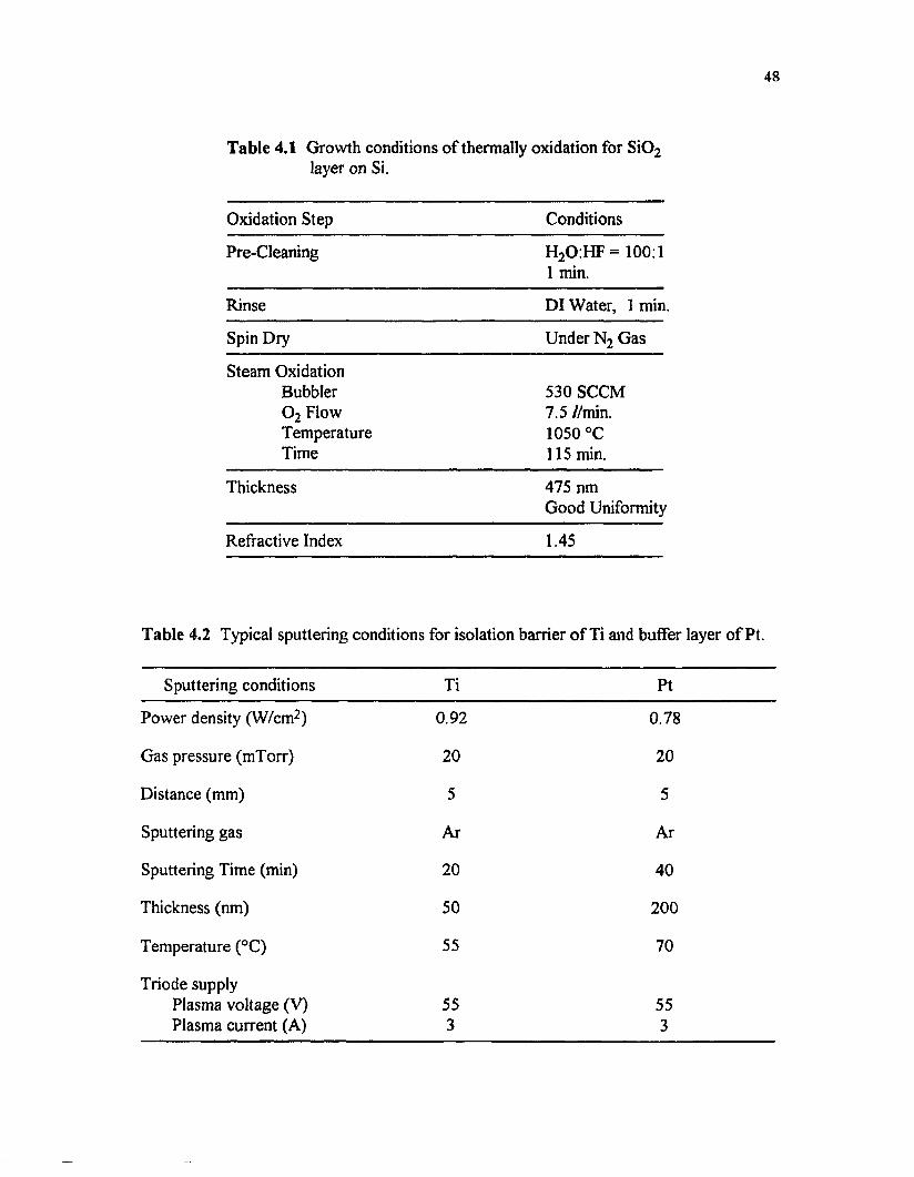
48
Table 4.1 Growth conditions of thermally oxidation for Si02 layer on Si.
Oxidation Step Conditions
Pre-Cleaning H20:H F= 100:11 min.
Rinse DI Water, 1 min.
Spin Dry Under N2 Gas
Steam OxidationBubbler 530 SCCM0 2 Flow 7.5 //min.Temperature 1050 °CTime 115 min.
Thickness 475 nmGood Uniformity
Refractive Index 1.45
Table 4.2 Typical sputtering conditions for isolation barrier of Ti and buffer layer of Pt.
Sputtering conditions Ti Pt
Power density (W/cm2) 0.92 0.78
Gas pressure (mTorr) 20 20
Distance (mm) 5 5
Sputtering gas Ar Ar
Sputtering Time (min) 20 40
Thickness (nm) 50 200
Temperature (°C) 55 70
Triode supplyPlasma voltage (V) 55 55Plasma current (A) 3 3

49
serious adhesion problem, a peeling-off phenomena due to its high thermal expansion
coefficient. It is usual to use Ti, Ti02, or Ta thin layer to solve the problems of thermal
and interfacial stability. Currently, Sreenivas et al [56] have studied the stable
metallization of Pt/Ti bilayer under the various environments for ferroelectric thin film
capacitors. Kondo et al [57] and Olowolafe et al [58] reported that the material behavior
of Ti and Pt was investigated to improve the adhesion with the substrate.
4.2 Target Design
The target sources of magnetron sputtering technique for multi-component ferroelectric
thin films are generally specified in 3 ways as shown in Figure 4.1. Magnetron sputtering
has special and considerable advantages in the range of usable plasma pressure, and in
limiting electron bombardment of the film. Figure 4.1 (a) shows the rf sputtering method
of a ceramic oxide pallette or mixed powder oxide target. Since the components of
powder oxide may have widely different sputtering yields, the target composition must be
adjusted by the amount of each component, as well as the additional PbO which is
normally added to the target to compensate for loss of Pb from the sputtered thin films.
However, the powder target process shows a number of disadvantages including [59,60]:
( 1) difficulty in pressing a large-diameter disk,
(2) target cracking due to heating during sputtering,
(3) reproducibility problem in terms of oxygen deficiency and stoichiometric variations on
the target surface, and
(4) low sputtering rate.
As described above, there is a limit in the strict control of film composition for such a
sputtering system with powder target. Figure 4 .1 (b) shows dc or rf reactive sputtering of
a multi component metal target, while Figure 4.1 (c) shows the reactive sputtering using
multiple metal targets. It is known that the sputtering rate of a metal target is higher than
the rate of oxides and insulators [59], Although the evidence is not yet conclusive, the

50
rfPower
(a) Ceramic powder Target
Power
(b) Multi-component Metal Target
dc Power
(c) Multiple Targets
Figure 4.1 Sputtering depositions of compound ceremic oxide films with different target formations.

51
sputtering rate for metal targets or a multi-component target is a factor o f 2 or 3 higher
than for a ceramic powder target, and lower substrate temperature processing is possible.
The multi-component metal target offers a number o f advantages. They include [61,62]:
( 1) the potential for higher sputtering rates due to smaller binding energy.
(2) the possibility for larger area target,
(3) high stability and purity of target,
(4) convenience of modification of the target composition, and
(5) the ability to incorporate dopant metal such as a La o f lead titanate.
A reactive magnetron sputtering system that can control the target areas of individual
metal elements is highly desirable for the preparation of the complex compound films. In
order to control, interdependently, each metal element in PLT thin films, a reactive
magnetron sputtering system with a multi-component metal target is used for the PLT
deposition in this study.
The task, to deposit high-quality material, is to produce films with low impurity
and correct stoichiometric composition. Target metals of multi-component film should be
extremely pure. The original metals of the multi component target consist o f Pb
(99.999%), La (99.9%), and Ti (99.97%). Several sectors of La, and a thin circular plate
of Pb, are located on a 2.25 inch diameter and 0.25 inch thick disk-shaped Ti target. A
typical schematic diagram of the multi component metal target is given in Figure 4.2. The
number of atoms deposited onto a unit area on the substrate is determined not only by the
target configuration, the incident ion energy, sputtering yield, and magnetron design, but
also by complex scattering phenomena within the plasma. Thus, the simple expression of
the number of atoms, n, modified by Ochiai et al [63] is written as:
n = agYt
where, a is a constant depending on the sputtering conditions (gas pressure, target power,

52
H
Figu
re 4
.2 M
ulti-
com
pone
nt m
etal
targe
t de
sign
for P
LT
film
.

53
and plasma current, etc.)
g is a geometric factor,
7 is the sputtering yield (atoms/ion), and
t is the sputtering time.
The content of an element in the deposited films is proportional to the fraction o f the
element in the multi-metals target. As proposed by Fukami et al [64] and Hase et al [65],
the ratio of the Pb/La area on Ti disk target is actually determined by the modified
Sigmund's method [66,67] which considers (1) sputtering yield for Pb, La, and Ti metal,
(2) Ti diameter due to (Pb+La)/Ti = 1/1, (3) composition ratio of Pb/La on the deposited
thin films. The film composition predicted for the /th element (C/) is given by:
C, = -= ~ — x 100 (atom %)
where, i corresponds to Pb, La, and Ti for PLT material,
Y: is the sputtering yield, and
Ai is the occupied area on the target.
The area ratio of each metal element on the target surface is estimated from the above
formula. The relative composition for the paraelectric PLT (28; i.e., Pb0 72Lao.28 0.93O3)
film is calculated to be:
Pb : La : Ti = 14.08 : 11.70:74.22
in the target area of each metal. The exact chemical composition of post-annealed PLT
thin films is characterized by Rutherford backscattering (RBS) and Auger electron
spectroscopy (AES).

54
4.3 Sputtering Conditions
A reactive magnetron sputtering is carried out by introducing an oxygen (purity 99.99 %)
and argon (99.999 %) gas mixture. Sputtering parameters such as power, sputtering
pressure, gas composition, substrate-target distance and substrate temperature thoroughly
affect the physical and chemical characteristics of the deposited PLT films. The details of
the multi-component target and sputtering conditions used in this experiment are
summarized in Table 4.3. The substrate temperature was measured by a chromel-alumel
thermocouple attached to the substrate holder. Table 4.4 shows partial pressures in the
chamber during PLT deposition using magnetron sputtering with a multi-component metal
target.
The primary factors, in the preparation and crystallization of PLT thin films, are
the adjustable control of oxidation kinetics and of the Pb content of the films, because Pb
tends to re-evaporate from the substrate at high temperature. Generally, the sputtering
rate in reactive sputtering deposition decreases rapidly with increasing oxygen partial
pressure. When the oxygen partial pressure is high, the surface of the target metals is
oxidized and an altered thin layer is formed. Oxygen gas pressure, dependent on the
sputtering rate, is completely different among Pb, La, and Ti metals. The oxidation
decreases with an increase in sputtering power and increases with an increase in partial
pressure of oxygen. The applied power must be greater than the threshold for each
component in order to maintain constant sputtering conditions and uniform composition in
the final films for a multi-component metal target [68],
In plasma processing techniques such as a reactive magnetron sputtering
technique, various target-substrate geometries can affect the deposition process of multi-
component oxide films. Consequently, there are several control problems which should be
considered in the stoichiometry of multi-component thin films using a reactive magnetron
sputtering method [69,70].

55
Table 4.3 Optimized sputtering conditions for PLT deposition.
Sputtering conditions PLT thin films
Power density (W/cm2) 0.86
Gas pressure (mTorr) 20
Target-substrate distance (cm) 4
Sputtering gas % P II o o
Deposition rate (nm/min) 2.8
Thickness (nm) 200
Substrate temperature (°C) 160
Triode supplyPlasma voltage (V) 60Plasma current (A) 3
Table 4.4 Partial pressure in the sputtering chamber after introducing the gases.
Material / Mass Factor Torr
Hydrogen 2.319 2.4 E - 8
Helium 7.143 NA
Water 1.333 4.6 E - 7
Nitrogen / CO 1.029 8.0 E - 8
Oxygen 1.053 2.5 E - 6
Argon 0.947 2.7 E - 6
Emulation 1.20 KV Total pressure 2.5 E - 5

56
(1) The formation of an altered layer at the target surface due to the different sputtering
yields in the multi-component target, the different diffusion coefficients, the concentration
gradient, and the temperature gradient
(2) The different composition between the target surface and the deposited film due to the
complex sputtering phenomena, particularly reactive processing
(3) Resputtering in terms of negative ion effects
(4) Electron bombardment effect by secondary electrons emitted from the oxide target
Many technical methods have been proposed in order to improve these disadvantages in a
magnetron sputtering process. Adachi et al [71] increased the operating pressure to
reduce the energy of the neutralized negative ions in terms of causing multiple collisions
for the plasma procedure. Sandstrom et al [72] and Terada et al [73] reported
unconventional sputtering geometries (so called, off-axis sputtering) to minimize the
bombardment of growing films by secondary electrons and ions emitted from the target.
The bias sputtering mode, in addition, is able to influence the properties of the deposited
films by changing the sputtering flux and energy of incident particles [74], The charged
particles are controlled by changing the electric field of bias sputtering. In multi-
component oxide sputtering, the constituent elements arriving at the surface of the
substrate usually have different sticking coefficients, especially if the elements have large
differences in vapor pressure. The sticking coefficients can also be changed by low energy
ion bombardment of the growing film by applying a small bias to the substrate [53], and
this bias sputtering is important in small adjustments of the stoichiometry.
The reactive sputtering deposition for good oxide films is governed by the
processes [75,76]:
(1) formation of a reproducible oxide layer on the target surface,
(2) the stability of the oxide species formed during transport in the plasma, and
(3) nucleation and growth on the substrate surface.

57
In this study, the specific techniques, such as off-axis sputtering and bias sputtering, are
not taken into consideration, owing to the low deposition rate and intricate plasma process
in the reactive sputtering method with triode and magnetron system. The operating
pressure used, 20 mTorr, is known to be a relatively high pressure in the magnetron
sputtering processes, to suppress the energy of negative ions as discussed by Adachi et al
[71]. In order to control the composition of deposited PLT films in spite of the different
composition between target surface and growth films, the modified Sigmund's method is
used under the optimizing sputtering conditions.
4.4 Post-Annealing Conditions
The most difficult factor to control in the stoichiometric composition of PLT films is the
Pb concentration, A non-stoichiometry of Pb content results from evaporation by heat
treatment such as substrate temperature during the deposition or post-deposition annealing
method. The heated substrate process influences the overall plasma phenomena of
reactive sputtering, and consequently an excess Pb content is required in the target
composition. Therefore, the post-deposition annealing for as-deposited PLT thin films is
not only more preferential treatment, but it also can achieve a chemically stable compound
by the similar method with the formation of ceramic bulk films. PLT thin films deposited
reactively by magnetron sputtering are in the amorphous or partially amorphous state, and
the as-deposited films subsequently require a post-annealing heat treatment. Since
ferroelectric compound oxide films are normally processed at a very high temperature,
their characteristics such as structural, electrical and mechanical properties, change
especially with the annealing conditions during the cooling-down step. A heat treatment
followed by a slow cooling-down at high temperature can considerably relieve the internal
stresses of as-deposited thin films. The post-annealing process for perovskite structure of
paraelectric PLT film can strongly affect the film composition due to lead volatility. Pb
evaporation during annealing treatment can be particularly influenced by the annealing

58
conditions such as annealing temperature, annealing time, oxygen partial pressure and
starting composition. The post-deposition heat treatment introduces an interdependency
between composition and crystalline structure evolution. Simultaneous crystallization and
Pb vaporization produce a relation between composition and the crystallographic structure
that is dependent on the kinetic mechanism of two processes. The structural phases within
the PLT thin film after post-deposition annealing depend on the starting composition, the
amount o f crystallization, and the quality of lead oxide volatility [26],
In our experiments, the substrate heat has not been used during the reactive
magnetron sputtering deposition of PLT in order to minimize the unbalanced effect in the
deposition rate of each metal element [61,62], suppress the Pb evaporation and reduce the
inter-reaction between the PLT film and substrate. The PLT thin films were annealed in a
fused quartz tube furnace with flowing oxygen at a flow rate of 0.2 //min. In the annealing
profile for all PLT films, the heating rate was 15 °C/min and the cooling rate was 5~6 °
C/min. The ranges of the annealing temperature and annealing time for this experiment
were 450~750 °C and 5~60 min, respectively.
4.5 Metal-Dielectric-Metal Capacitor
Metal-dielectric-metal (MDM) structures for electrical and dielectric measurements are
fabricated on multi-layer (Pt/Ti/Si02/Si) and MgO substrates as shown in Figure 4.3 (a)
and (b). Through a suitable choice of the electrode material and the deposition method for
the ferroelectric ceramic oxides, it is possible to control the electrical properties o f the
MDM structure and in particular to influence the electrical resistance. The effect o f the
electrode material, on the electrical properties of ferroelectrics, has not been completely
studied yet.
However, contact between the electrode metal and the ferroelectric oxides is
generally specified by neutral, ohmic and barrier type [77,78], In the case o f neutral
contact, the electronic work functions o f the metal (Wm) and the ferroelectric oxides (Wf)

59
(b) P
t/PLT
/Pt-M
gO
subs
trate
.

60
are equal, while the conditions o f ohmic and barrier contacts are Wm>Wf and Wm<Wf,
respectively. The barrier contacts form a high specific electrical resistance, owing to a
depletion layer occurring at the metal-ferroelectrics interface. This is the reason for
nonlinearity in the current-voltage characteristic curves. Therefore, the electrodes on
MDM capacitor should be of ohmic contact, so that they present a small electrical
resistance and good adhesion at the interface, and do not cause changes in the electrical
properties of the ferroelectric oxides. Magnetron sputtering to obtain ohmic electrodes
for paraelectric PLT thin films is a known deposition method. Among the various
electrode materials, Pt as a top and bottom electrode is also used because of the potential
advantages in its electrical characteristics.

CHAPTER 5
MATERIAL ANALYSIS AND DISCUSSION
Paraelectric lead lanthanum titanate (PLT; 28 mol %) thin films are prepared by a multi-
component metal target using the previously described magnetron sputtering system. The
as-deposited amorphous films are crystallized into the cubic (or paraelectric) perovskite
structure by a heat treatment at an annealing temperature ranging from 450 to 750 °C.
The post-annealing treatment, used for crystallizing the films in this study, affects the film
composition due to Pb evaporation. The electrical properties o f the perovskite PLT thin
films are strongly dependent upon the stoichiometric composition and crystalline structure.
The dielectric properties of the films reach maximum values near the ferroelectric-
paraelectric phase boundary (La content o f 28 mol %) in the equilibrium phase diagram of
PLT system as previously mentioned in Chapter 2. Therefore, it is necessary to analyze
the material characteristics of PLT thin films such as chemical composition, crystalline
structure and surface microstructure.
The primary concern in PLT (28) thin film deposition is the stringent control of
stoichiometric composition. AES (Perkin-Elmer, PHI 660, scanning Auger microscopy)
and RBS (General Ionex, model 4117, Tandetron ion accelerator) measurements are used
for analyzing the relative composition ratio of Pb, La, Ti and O of the PLT thin films. The
depth profiles of the films are also measured using AES, and the exact thickness o f PLT
(28) thin films is identified by RBS analysis. The crystalline phases and lattice parameters
of thin films is characterized by an X-ray diffractometer (Rigaku, D/MAX system and
philips, vertical diffractometer) using CuKa radiation. The microstructure of the films is
also investigated by SEM (ISI, SIII-A(K)).
61
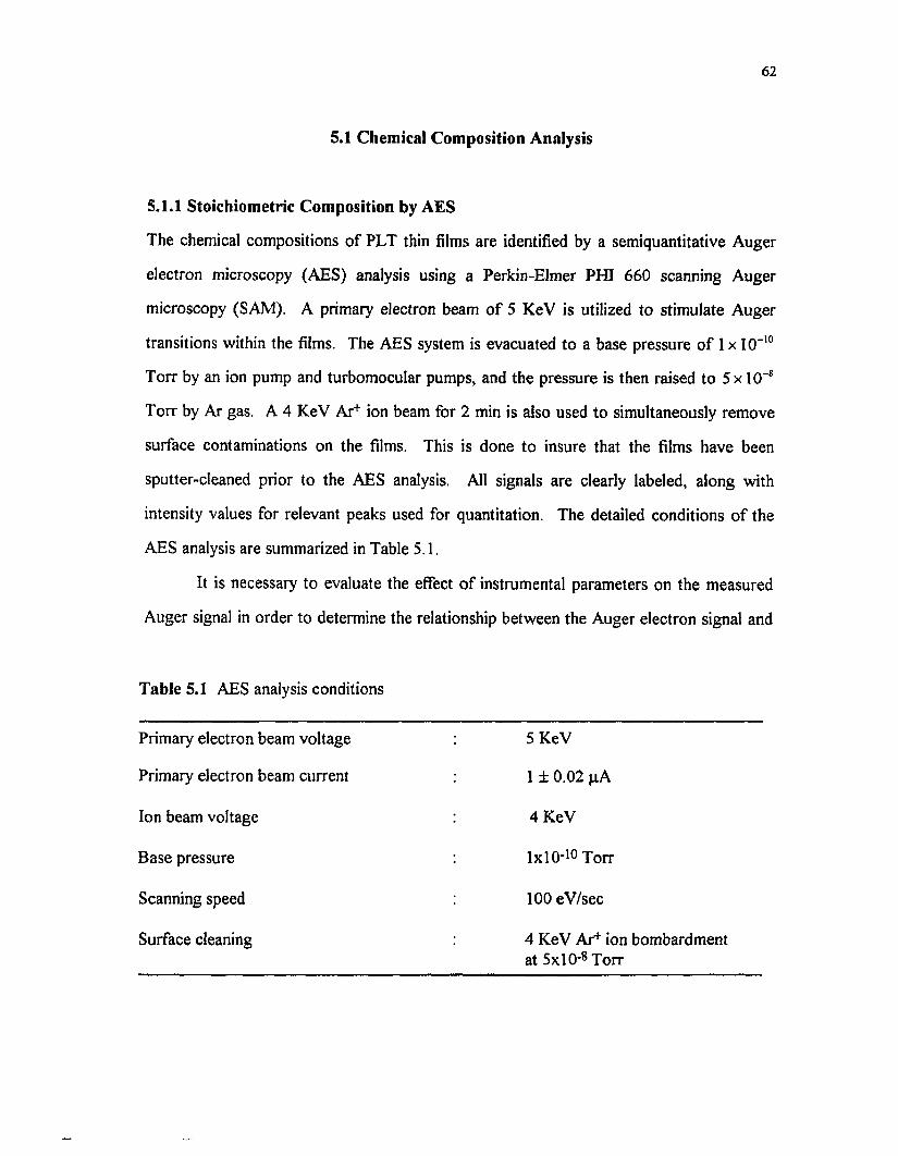
62
5.1 Chemical Composition Analysis
5.1.1 Stoichiometric Composition by AES
The chemical compositions of PLT thin films are identified by a semiquantitative Auger
electron microscopy (AES) analysis using a Perkin-Elmer PHI 660 scanning Auger
microscopy (SAM). A primary electron beam of 5 KeV is utilized to stimulate Auger
transitions within the films. The AES system is evacuated to a base pressure of 1 x IO-10
Torr by an ion pump and turbomocular pumps, and the pressure is then raised to 5 x 10' 8
Torr by Ar gas. A 4 KeV Ar+ ion beam for 2 min is also used to simultaneously remove
surface contaminations on the films. This is done to insure that the films have been
sputter-cleaned prior to the AES analysis. All signals are clearly labeled, along with
intensity values for relevant peaks used for quantitation. The detailed conditions of the
AES analysis are summarized in Table 5.1.
It is necessary to evaluate the effect of instrumental parameters on the measured
Auger signal in order to determine the relationship between the Auger electron signal and
Table 5.1 AES analysis conditions
Primary electron beam voltage
Primary electron beam current
Ion beam voltage
Base pressure
Scanning speed
Surface cleaning
5 KeV
1 ± 0.02 pA
4 KeV
lxlO-10 Torr
100 eV/sec
4 KeV Ar1- ion bombardment at 5x10'8 Torr

63
the atomic concentration. The important instrumental variables are the primary electron
beam current, the primary beam energy and the dN(E)/dE spectrum. Figures A.l, A.2 and
A.3 are Auger energy spectra of each pure Pb, La or Ti metal. These values are very
similar to the data values of pure elements tabulated in a handbook of Auger electron
spectroscopy [79]. In Figure A. 1, the Auger spectrum of pure Pb shows only a Pb peak at
93 eV. Ti Auger signals, as shown in Figure A.3, are detected at 386 eV and 417 eV.
However, the Auger spectrum of pure La, as shown in Figure A.2, indicates La signals at
82 and 631 eV, and an intense O signal at 516 eV because La oxidizes rapidly in air. The
surface of pure La metal is quite rough and appears to be porous.
A simple approximation of quantitative analysis can be accomplished by a
comparison of Auger signal intensity in the test sample to that of the pure elemental
standard. The elemental atomic concentration of element, Cx, in the test sample is
expressed as:
c Ix(test)* Ix (standard)
where Ix (test) and Ix (standard) are the peak-to-peak Auger signal intensity from the film
and standard, respectively. The atomic concentrations of PLT thin film, however, can not
be calculated directly from the Auger energy spectra of pure elements. There are several
inherent sources of error in the above formula. The most important factors are: (1) matrix
effects on the Auger electron escape depth and backscattering factors, (2) chemical effects
on peak shapes, and (3) surface topography [79,80], The Auger electron escape depth in
the test film may be different from that of the pure elemental standard. Since the
magnitude of the Auger signal is proportional to the number of atoms in the analysis
volume, a larger escape depth will cause a corresponding increase in the Auger signal.
Chemical effects can change the peak shape and thus lead to an error when using peak-to-

64
peak heights in the differentiated spectrum for a measurement o f the Auger signal. A
smooth surface generally produces a larger Auger signal than a rough surface [80],
Besides, surface roughness on the films will degrade the Auger signal intensity. This
effect is minimized by determining concentrations from the above equation since surface
roughness is expected to decrease all Auger peaks.
A standard of known composition, which is close to that of the actual films, should
be used to obtain the highly accurate quantitative analysis. Figure A.4 shows the energy
spectrum and relative composition o f a perovskite PLT thin film analyzed by Rutherford
backscattering spectrometry measurement. RBS results o f PLT ceramic oxides, which are
chosen as a composition standard, are used to calibrate the Auger transition intensities, in
order to increase the semiquantitative accuracy of the Auger technique. Figure A. 5
presents the Auger spectrum for the same PLT film with the result of RBS analysis.
Elemental relative sensitivity factors of the perovskite PLT thin films for semiquantitative
analysis are calculated from AES analysis based on the RBS results. The atomic
concentration for each element in a PLT film can be obtained by multiplying the peak-to-
peak height by an elemental relative sensitivity factor. Table 5.2 shows relative Auger
peak-to-peak height and relative sensitivity factors for a PLT film. These values are
Table 5.2 Relative Auger peak heights and relative sensitivity factors for a standardPLT film.
Elements and peak voltage (eV)
Peak-to-peakheight
Atomicconcentration
Relative sensitivity factor (RSF)
Pb, 93 175.6 0.144 1.182
La, 626 19.2 0.044 0.511
Ti, 418 56.4 0.132 0.555
O, 511 248.9 0.680 0.400
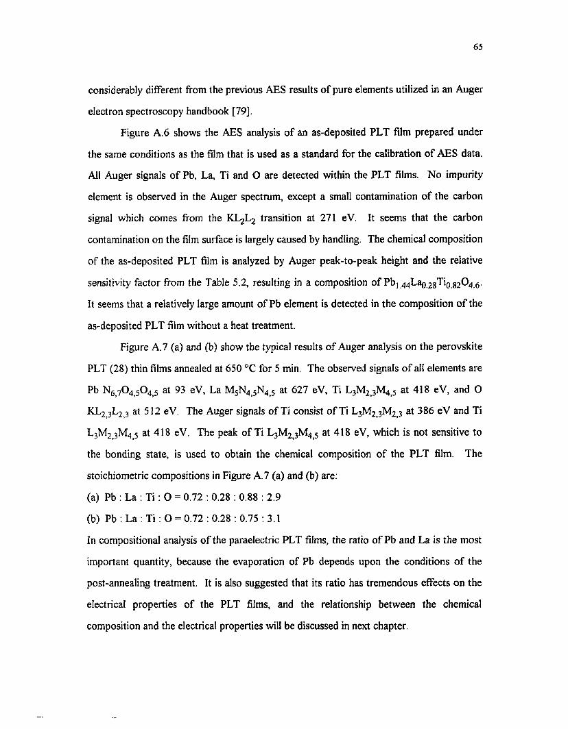
65
considerably different from the previous AES results of pure elements utilized in an Auger
electron spectroscopy handbook [79].
Figure A.6 shows the AES analysis of an as-deposited PLT film prepared under
the same conditions as the film that is used as a standard for the calibration of AES data.
All Auger signals of Pb, La, Ti and O are detected within the PLT films. No impurity
element is observed in the Auger spectrum, except a small contamination of the carbon
signal which comes from the KL2L2 transition at 271 eV. It seems that the carbon
contamination on the film surface is largely caused by handling. The chemical composition
of the as-deposited PLT film is analyzed by Auger peak-to-peak height and the relative
sensitivity factor from the Table 5.2, resulting in a composition of Pb] 44Lao 28Tio.s2O4.6-
It seems that a relatively large amount of Pb element is detected in the composition of the
as-deposited PLT film without a heat treatment.
Figure A. 7 (a) and (b) show the typical results of Auger analysis on the perovskite
PLT (28) thin films annealed at 650 °C for 5 min, The observed signals o f all elements are
Pb N670 450 45 at 93 eV, La MSN4>5N4>5 at 627 eV, Ti L3M2>3M4i5 at 418 eV, and O
KL2 3L2 3 at 512 eV. The Auger signals of Ti consist of Ti L3M23M2 3 at 386 eV and Ti
L3M2i3M4 5 at 418 eV. The peak of Ti L3M2i3M4)5 at 418 eV, which is not sensitive to
the bonding state, is used to obtain the chemical composition of the PLT film. The
stoichiometric compositions in Figure A. 7 (a) and (b) are:
(a) Pb : La : T i : O = 0.72 : 0.28 : 0.88 : 2.9
(b) Pb : La : Ti : O = 0.72 : 0.28 : 0.75 : 3.1
In compositional analysis o f the paraelectric PLT films, the ratio o f Pb and La is the most
important quantity, because the evaporation of Pb depends upon the conditions of the
post-annealing treatment. It is also suggested that its ratio has tremendous effects on the
electrical properties of the PLT films, and the relationship between the chemical
composition and the electrical properties will be discussed in next chapter.

6 6
5.1.2 AES Depth Profile
Auger electron microscopy is also used to check the carbon contamination and the
composition uniformity across the thickness of paraelectric perovskite PLT thin films.
The Auger depth profile of the as-deposited PLT film on Pt/Ti/SiC^/Si, as a function of
etching time, is shown in Figure A.8. The amorphous PLT film is nonuniform near the
film surface, and the Auger data shows a Pb enrichment on the surface of the as-deposited
film. Although the higher Pb concentration in the near-surface region of the film can not
be explained precisely, the sputtering rate of Pb has been reported to be higher than that of
La or Ti metal [62,64], It would lead to an increasing slope in the Pb profile near the film
surface. A Pb enrichment on the surface region has also been observed from rf-magnetron
sputtering using a multi-target by Adachi et al [68], It seems that this effect is a general
phenomenon of the as-deposited film and is not related to a specific deposition method.
Carbon contamination is not observed in the depth profile of the amorphous PLT film
except for the carbon absorption on the film surface as shown in Figure A. 8.
The AES depth profiles for the post-annealed films are shown in Figure A.9 (a)
and (b). The AES profiles for PLT thin films annealed at 650 °C for 5 min are remarkably
different from that of the as-deposited film near the surface region. The Pb content o f the
heat-treated films decrease at the surface, suggesting that this fact is due to the
evaporation of Pb from the surface during the post-annealing process. The typical depth
profile shows relatively uniform distribution of the components (Pb, La, Ti and O) into the
depth of the film.
5.1.3 Rutherford Back-scattering Analysis
Rutherford back-scattering is used to investigate the stoichiometry of PLT thin films, as
well as to calibrate the Auger spectrum signal to an elemental concentration of AES
characterization. Figure A. 10 (a), (b), (c) and (d) illustrate the RBS spectra of the PLT
thin films with the different area ratio of a multi-component metal target. An annealing-

67
heat treatment for all PLT films is applied under the same condition at an annealing
temperature of 650 °C for 5 min. The changes o f the normalized compositions as shown
in the spectrum analysis of the RBS for each metallic components of PLT thin films shows
a similar tendency with the relative composition ratio in target area of metal elements. It
is mentioned that the content of an element in the deposited PLT films is proportional to
the fraction of the element in the target metal. It is noted that the relatively big signal of
oxygen is detected due to the inherent sensitivity of the RBS system.
5.1.4 Discussion
The atomic concentrations in ternary ceramic PLT films, as the results of compositional
analysis, could not be directly estimated by the comparison with the Auger spectra o f pure
Pb, La, and Ti as shown in Figure A.l, A.2 and A.3. The Auger signal of each element in
the PLT films is observed to be slightly shifted in comparison with the value of pure metal.
It is expected that the shift of the Auger peak signal is caused by matrix effects.
Therefore, the relative sensitivity factor for each element is calculated, and the results are
summarized in Table 5.2.
Compositional control of the PLT thin films is accompanied with the changes in
relative area ratio of the multi-component metal target. Figure 5.1 shows the relationship
between the relative composition of the perovskite PLT thin films and the corresponding
area ratio of the multi-component metal target specified by six different types. The black
star means the ideal composition ratio of paraelectric PLT (Pbo^Lag 2gTi0.93O3) thin film
in a ternary oxide Pb-La-Ti-0 system. The white star expresses the compositional area
ratio o f target element estimated by the modified Sigmund's method. Table 5.3
enumerates in detail the schematic results of Figure 5.1 analyzed by AES and RBS
measurements. The content of La is the important factor, in this study, because the
paraelectric state of the PLT thin films is determined by the La content in the phase
diagram of Pb-La-Ti-0 system as shown in Figure 2.3. The dielectric and electrical

6 8
Optimal composition
• Type A
O Type B
V Type C
V Type D
□ Type E
B Type F
PLT film composition
Ti
Relative ratio of target area
Pb
Figure 5.1 Relationship between the relative composition of sputtered PLT films and the corresponding area ratio of multi-component metal target.

69
oo
*43cducdoUrncd00c
*-3coCLC/3
£OCJ<L>
* c
§c/T
*33
*cd§
C/3
9>*J3GO
EEc2H-JCL,
0)SP
ocd4->
c,o*cd3
*■£3 E*eoO cCL <DB Co oo cl
(U E> o‘43 ucd . JL
*3Pi 3
EfOin0)s«H
c hZ0000 « n 00
ir>p *00 o
pIT)CS
PVov
o c o' o' © d *— * o'*53oQ.Eoo
”c3o
La
00CNo' 0.
28610 0.
22
0.24
0.26
0.28
£oj :O ^ 3
CNp~
CN CNr -
CN CNP -
cnPM
CNP~
P m o' o o' o' o' o' o
EUST 3w
• VOw v o0 0
MMOv
OvCN
om mCN
Ov
H v dr r
cn■d-
00p 00Tj- cn’ID
v di n
00•<r
•4M
oD .o
• ocd oo
oo
t~*v q
r>Ov
p - PMv q i n
o
. 2
hJ VO CNrM
cn^"4 c
t i-'
•*32
>*43cd JO
CNv q
TT CN T ft~»
CNi n
o oo^Mm
& e u 00P I
00 Ovc n
v d cn'P I t o
cd2
vor -
ovq
p-Ov "O' Ov00 P I
0 0<NCS
cd
3SPto•4M
C*MO
_ o
H i n00
■d-00
P-'0 0
o 'OV o v
cno v
T f
La 5.85 o00
p-' 4.41
4.41
4.41
4.41
11.7
0
2
. i15 Pb
00m00 7.
60
7.60
5.19
3.70
LL'Z 14.0
8
o
Type
s
c CQ U Q U U h1•aO
T 3*■4

70
characteristics, consequently, depend on the paraelectric perovskite phase. In order to
compare the AES analysis of the PLT thin films with the chemical composition by the
general formula of the PLT system (Pbj.xLaxTij.^C^; La content of 28 mol %), the
accurate coefficients of the stoichiometric composition (Pb, La, Ti and O) for the
perovskite structure (AB03) should be 0.72, 0.28, 0.93 and 3, respectively. The close
composition of PLT films, as shown in Figure A.7 (a), is Pb of 0.73, La of 0.28, Ti of 0.88
and O of 2.9. In conclusion, the observed composition of the AES analysis shows that the
PLT (28) film deposited reactively by the multi-component metal target using a magnetron
sputtering system has a close stoichiometric composition. Furthermore, the criterion of
RBS analysis provides accurate quantitation in chemical composition of the paraelectric
PLT films to act as standards for AES characterization.
5.2 Crystalline Structure Analysis
5.2.1 Annealing Temperature Effect
The crystalline structure of the films is examined by X-ray diffractometer (XRD; 30 KV,
20 mA) using Cu K a radiation. The effect of a post-annealing treatment on XRD patterns
of paraelectric PLT thin films is presented in Figure A. 11. The preparation o f these films
is of the same thickness (200 nm) and annealed for the same time (5 min). The accurate
composition of these films belongs to the type D as shown in Table 5.3. As-deposited
PLT films produce XRD spectrum consistent with an amorphous structure. The
formation of a broad hump in the films treated annealing temperature below 450 °C shows
around 20 = 30 ° as shown in Figure A.l 1 (a). It has been reported that the structure of
PLT films under a heat treatment of low temperature may correspond to the metastable
pyrochlore phase [42,81]. The general formula of the pyrochlore is A2B20 7. The (100)
and (110) peaks do not appear clearly in as-deposited films. After PLT films are annealed
at a temperature above 550 °C, XRD patterns exhibit the formation o f the stable

71
perovskite phase as shown in Figure A. 11 (b), (c) and (d). Tetragonal splitting peaks of
perovskite structure are not observed on the XRD spectra of PLT films. Typical
diffraction peaks of the cubic perovskite phase such as ( 100), ( 110), (200) and (211)
orientation arise completely in all PLT films. The other peaks are identified as related to
the substrate, either Pt or Si. It seems that the intensity of each peak in XRD patterns
increases up to the highest temperature of 750 °C. The numerical data of XRD patterns,
as shown in Figure A.l 1, are also summarized in Table 5.4. The effect o f heat treatment
with increasing annealing temperature results in the increasing intensity for each peak,
while FWHM of each diffraction peak seems to be gradually reduced. Also, it is certainly
observed that the angular shifting of all difif action peaks trends toward a higher angle with
an increase of post-annealing temperature. It is expected that the films may be influenced
by changes of internal stress with increasing temperature [82] or by reduction of the
amount of Pb element incorporated within the cubic perovskite structure [22],
Figure A. 12 shows the XRD spectra of the paraelectric PLT films as a function of
annealing temperature for crystallization. The preparation conditions of these films are the
same; i.e., same thickness (200 nm) and same annealing time (5 min). The chemical
composition of these films belongs to the type A as illustrated in Table 5.3, and in
particular the film annealed at 650 °C exhibits the diffraction pattern with the
stoichiometric composition of Pbo.73Lao 28Tio.88O2.9- As-deposited PLT film presents the
broad amorphous pattern, and the (111) main peak and (200) peak of platinum (Pt) are
uniquely observed. Schwartz et al [43] and Dana et al [83] found that the (200) peak of
Pt was also detected in the XRD spectrum of the as-deposited PLT thin films with a
thickness of about 400 nm. On the contrary, Shimizu et al [81] reported that the Pt (200)
peak was not observed in the as-deposited PLT films with a thickness greater than 500
nm, and conversely the (200) peak of the perovskite PLT structure appeared only around
20 = 45.5 with a heat treatment of high temperature (up to 900 °C). It is expected, as a

72
oCNS"OO
CN00
o00CN
csvolO
oC*")cnO
ooooCN CN
CNOv
oCN
CN•va-tSts CN
cnVO*
cnOO
cs
ov©CN CS
cn
CScncscninO
CS
o cs
CDcs
Q .
Om

73
result of this study, that Pt (200) peak and PLT (200) peak of the XRD patterns may be
overlapped like the results of Schwartz et al and Dana et al.
The paraelectric perovskite phase according to the XRD patterns is detected for all
films in the temperature range of 550 to 750 °C. The trend of these XRD patterns
corresponds relatively to those of Figure A. 11. The film annealed at 650 °C shows a small
(210) orientation peak of the cubic perovskite structure. Also, the intensity o f each
diffraction peak is directly proportional to the effect of rising annealing temperature. The
sharpness of the peaks indicates good crystallinity in the perovskite PLT films. The heat
treatment of PLT (28) thin films at 650 °C for 5 min results in the formation of the
paraelectric perovskite structure with a lattice constant of a = c= 0.394 nm and oxygen-
to-oxygen distance of 0.279 nm.
Figure A. 13 demonstrates XRD step scans over the angular range from 20 = 54 to
20 = 59 in order to observe the (211) peak shift of the films annealed at 550, 650, and 750
°C. This peak shifts ffom d = 0.1633 nm to d = 0.1609 nm with a rise of annealing
temperature. It seems that the slight shift is due to the changes of compressive stress in
the internal film and Pb evaporation within the perovskite phase with increasing
temperature.
Figure A. 14 presents the diffraction pattern as a function of temperature for the
PLT films of a chemical composition type B as shown in Table 5.3. At 550 and 650 °C,
both PbO around 20 = 30 and polycrystalline perovskite phases coexist, because of the
excess Pb content as shown in Figure 5.1. The perovskite peaks are observed at 750 °C
only, and the PbO peaks completely disappear at high temperature. Sayer [61] reported
that the crystallization of amorphous ferroelectric films was initiated around 400 °C and
completed between 600 and 700 °C, depending on the film preparation method and
annealing conditions. It is suggested that, for a good characteristic of PLT thin films, the
relationship between the composition and the crystal structure caused by Pb evaporation is
interdependent.

74
Figure A. 15 illustrates the XRD spectra of PLT thin films on a single-crystal MgO
(100) substrate. As-deposited film shows only one peak of MgO substrate and amorphous
phase along the diffraction spectrum. Two peaks o f the perovskite PLT film appear, and
their intensities are increased with changes o f annealing temperature. It is thought that
the PLT films deposited on MgO substrate suffer compressive stress along the crystalline
plane of the films by an annealing heat treatment. Hence, this stress may transform the
polycrystalline films into c-axis and a-axis oriented films [84].
5.2.2 Annealing Time Effect
Figure A. 16 shows the XRD patterns of the perovskite films as a function of annealing
time at the annealing temperature of 650 °C. As-deposited film is obviously amorphous,
and the (111) peak of platinum and other substrate peak is observed. In the PLT (28) thin
films annealed at 650 °C, an elevated annealing time shows only the typical formation of
the perovskite phase, and the intensity of the diffraction peaks increases further. It is
apparent that the slight shift o f typical PLT peaks occurs in the films annealed for a
prolonged annealing period.
5.3 Surface Microstructure Analysis
It is known that as-deposited thin film presents microstructures of densely packed fiber
with a smooth surface as shown in SZM zone I or zone T of Figure 2.4 [27], The as-
deposited PLT film is smooth and shows a featureless surface as exhibited in Figure A. 17.
This shiny morphology of the as-deposited films is expected to be modified by a post
annealing treatment. Figure A. 18 presents a typical SEM topography for the PLT thin
film annealed at 650 °C for 5 min. It is likely that the film surface is also relatively
smooth, and belongs to the SZM zone II. The segregation phenomena on the delimiting
surface of the PLT (28) thin film annealed at 750 °C for 5 min are shown in Figure A. 19.
Murakami et al [85] and Opila [86] have reported that the segregation along grain

75
boundary appears frequently in Pb-based ceramic films in the presence of oxygen due to
Pb evaporation. It is suggested that this phenomena occurs to reduce thermal strain within
the film during post-annealing treatment. However, the films deposited by substrate heat
treatment shows relatively less segregation because the phase formation grows slowly
without the evidence of a remarkable grain boundary.
Figure A.20 (a) and (b) show cracking on the multi-layer substrate and a lack of
adhesion on MgO substrate in terms of the post-annealing treatment o f high temperature
at 750 °C for 60 min. High temperature annealing, in particular, results in thermal
segregation by Pb evaporation and grain densification, and finally leads to the formation of
hillocks or craters. The serious crack, caused by the prolonged heat treatment, is
accelerated by thermal stress in terms of a mismatch in thermal expansion coefficients
between PLT film and substrate.

CHAPTER 6
ELECTRICAL ANALYSIS AND DISCUSSION
All electrical measurements for DRAM application are performed utilizing a MDM
configuration capacitor using the paraelectric PLT (28) thin films of 200 nm thick as a
dielectric layer. Dielectric measurements are carried out on a Boonton 7200 capacitance
meter with a peak voltage of 10 mV (i.e. 500 V/cm) and a frequency of 1 KHz. The most
frequently used test to characterize ferroelectric or paraelectric PLT thin films is a typical
Sawyer-Tower circuit [87], This is an excellent measurement technique for establishing
the relationship of polarization to electric field. Polarization-electric field (P-E)
characteristics for charge storage density is investigated by an HP54501A digitizing
Oscilloscope and Wavetek (Model 270) Function Generator. Additional electrical
characteristics such as, current-voltage (I-V) plot for leakage current density and voltage
time (V-t) measurements for charging transient, are of interest for a capacitor dielectric of
the 1-T DRAM cell. These topics are the subject of reliable characteristics and the
transient behavior o f paraelectric PLT (28) thin films. The current-voltage characteristics
for leakage current density are measured by an HP4145B Semiconductor Parameter
Analyzer.
6.1 Dielectric Characteristics
6.1.1 Effect of post-annealing temperature
The dielectric constant and dissipation factor (loss tangent) as a function of post-annealing
temperature are presented in Figure 6.1. The dielectric constant increases significantly and
the dissipation factor decreases slightly, as the annealing temperature is increased. The
dielectric properties are dependent on the changes in the stoichiometric composition as
76

Diele
ctric
cons
tant
77
1200 -
900 -
600 -
0.060.05
-0 .040.030.020.01
300 -
650 750550450
Annealing temperature [°C]
Figure 6.1 Dielectric constant and dissipation factor of PLT (28) thin films as a function of post-annealing temperature.
Dissi
patio
n fa
ctor

78
well as in relative quantities of amorphous and crystalline structures with variation of
annealing heat treatment. Thus, with a rise in annealing temperature, the amorphous
phase and the excess PbO structure with poor dielectric properties disappear and are
transformed to the ciystalline structure, i.e., the paraelectric perovskite PLT phase.
Conversely, the dissipation factor reduces from 0.051 to 0.018 with the increasing
annealing temperature, and with the dependence on the existence of the amorphous and
excess PbO phases.
The dielectric constant of the PLT thin films, in this study, is sometimes difficult to
measure, because of the low resistance of the films and the presence of microcracks and
porosity caused by high temperature treatment. Fox et al [88] have commented that the
dielectric properties can be expressed by morphological conditions of the thin films with
coexistence of the three phases such as perovskite PLT phase, excess PbO and air. The
excellent dielectric properties of PLT thin films are achieved by the continuity o f the
perovskite PLT phase. The PbO phase and porosity resulting from Pb evaporation give
rise to the discontinuity of the perovskite PLT phase in the thin films. The PbO phase has
a higher conductivity than the perovskite PLT phase. The dielectric constant decreases
and the dissipation factor increases due to the presence of excess PbO phases in the films
annealed at lower annealing temperature.
6,1.2 Effect of temperature
Figure 6.2 shows the relative dielectric constant of the PLT film annealed at 650 °C and
for 5 min at the temperature range of 30~120 °C. The dielectric constant of paraelectric
PLT (28) thin film decreases slightly as a fiinction of temperature. The peak of dielectric
constant, the so called Curie temperature, is not observed in this temperature range. It is
expected that the dielectric peak of the film with the change of temperature is similar to
the Curie temperature reported by Keizer et al [29],

[%] ooi xr0?/?;
79
100
8 0 -
6 0 -
4 0 -
2 0 -
90 13030 7050 1 1 0
Temperature [°C]
Figure 6.2 Dielectric constant of 200 nm PLT (28) thin film with different tempersture.

80
6.1.3 Effect of La content in PLT films
The dependence of the dielectic constant on various La concentrations of PLT thin films is
demonstrated in Figure 6.3. All PLT films are annealed by the same condition of post
deposition heat treatment at 650 °C for 5 min. The dielectric constant increases with a
rise in La concentration. This phenomenon results from the lowering of the Curie
temperature, as shown in the results of Adachi et al [42]. This is due to the La content
increases slightly in the chemical composition of the PLT films. The dielectric properties
are closely related to the changes in chemical composition of PLT thin films. The
dielectric constant and dissipation factor of PLT (28) thin film are around 904 and 0.023,
respectively.
6.1.4 Discussion
The perovskite PLT phase, from the results o f various effects mentioned above, primarily
exhibits (100) orientation for nearly stoichiometric composition. However, it may be
noted that small changes of the composition and crystallinity produce substantial changes
in the dielectric characteristics of the PLT thin film. The main reason for a poor dielectric
properties at low annealing temperature may be explained by low crystalline phases of the
PLT films. Since the intensities of the perovskite phases increase with an increase in post
annealing temperature as illustrated by the results of XRD patterns, it is expected that the
dielectric characteristics of paraelectric PLT thin films correspond well with the crystalline
structure and the excellent dielectric properties of PLT thin films are achieved by the
continuity of the perovskite structure. The best results of dielectric constant and
dissipation factor at low field measurement (500 V/cm), as shown in Figure 6.1, are
approximately 1216 and 0.018 in Pt/Ti/Si02/Si substrate, respectively. Actually, the
measured dielectric constant is tremendously different from the value of bulk PLT films
reported by Hennings et al [22], It is supposed that porosity and the segregation

Die
lect
ric
cons
tant
81
1000
800
600
400
200
0
28 30
La concentration
Figure 6.3 Changes of the dielectric constant with increasing La concentration of PLT films as described in Table X.

82
phenomena produced by Pb evaporation considerably affect the dielectric properties of
PLT thin films.
6.2 Polarization-Electric Field Characteristics
The polarization-electric field (P-E) characteristics of the paraelectric PLT (28) thin films
are measured using a typical Sawyer-Tower circuit with a 500 Hz sine wave as shown in
Figure 6.4. The P-E measurements of the films under different peak voltages are
presented in Figure B. 1. The paraelectric PLT (28) thin film is annealed at 650 °C for 5
min. The P-E curve at low peak voltage of 1 V (50 KV/cm) is similar with the linear
behavior of a normal dielectric material as shown in Figure B.l (a). The P-E
characteristics are gradually developed to the paraelectric state of nonlinear behavior, as
the peak voltage increases enough. The charge storage density (or polarization) is around
10.3 pC/cm2 at the peak voltage of 4 V (200 KV/cm). The polarization is proportional to
the electric field, and the relative dielectric constant is constant by means of the formula,
P=£0(Sr-1 )E, only at a low field. The polarization is gradually saturated with the
increasing peak voltages, due to the paraelectric characteristics, and the above equation
for dielectric properties can not be automatically applied to the paraelectric phase. The
approximation of dielectric constant with different peak voltage is obtained by the
effective dielectric constant, Kep defined as the following [20]:
K -~ rr
max
where, Q'c is the charge storage density, and Emax is the maximum electric field. The
above mentioned equation shows that the effective dielectric constant is approximately
580 at a peak voltage of 4 V.

83
Functiongenerator
peak voltage: 1,2 and 4 V at 500 Hz
-O V,
'P E
-o V.
Thickness : 200 nm Area : 3.14 x 10⁴ pm2 CPE: 1.26 and 1.69 nF C0 : 68.7 nF
Function generator : Wavetek Model 270 Digitizing Oscilloscope: HP54501A
Figure 6.4 Typical Sawyer-Tower circuit for polarization-electric field measurement.

84
Figure B.2 shows the P-E characteristics with different peak voltage for the PLT
(28) film heat-treated at 750 °C for 5 min. The P-E curve at a peak voltage of 2 V
presents the prominent paraelectric nonlinear behavior. The charge storage density at the
peak voltage of 4 V (200 KV/cm) is around 12.5 pC/cm2 as shown in Figure B.2 (c), and
the effective dielectric constant is about 706. Figure B.3 describes the P-E characteristics
as a function of annealing temperature at the same peak voltage of 4 V. The formation of
the paraelectric state in PLT (28) films with increasing post-annealing temperature is
obvious at a glance from this Figure. It is expected that some degree of crystallinity, with
different annealing temperature, has an influence upon the paraelectric nonlinear
characteristics of the films.
Recently, Adachi et al [1] reported that the polarization of PLT (28) thin films
exhibited a slim hysteresis loop. But the La contents of 28 mol % in their films were the
chemical composition in the powder target of rf-magnetron sputtering. Therefore, the La
contents of PLT thin films were practically lower than those of target material, and their
P-E hysteresis with slim loop obviously showed the ferroelectric behavior of PLT thin
films.
6.3 Leakage Current Characteristics
The leakage current density is one of important limiting factors for the DRAM capacitor
dielectric. High leakage current places important limitation in the operation of a unit cell.
It is necessary, to prevent the capacitor from discharging between refreshing cycles, that
the leakage current per unit area should be low. There are several transport mechanisms
of leakage current in a MDM capacitor [38,89], and also there are two distinct regions
specified by the electric field. Ohmic behavior is the dominant process at low electric
fields. The leakage current density of ohmic characteristics is expressed:

85
where, E is the applied electric field,
A is a constant related to thermally excited electron hopping, and
Ea is the activation energy.
Under high fields, the leakage current exhibits exponential behavior which is governed by
oxygen vacancy diffusion, space charge limit current injection, grain boundary potential
barrier, tunneling, Schottky emission, or Poole-Frenkel emission [90], The leakage
current characteristics of PLT thin films vary exponentially with the square root of the
electric field. This is mainly due to Schottky emission or Poole-Frenkel emission of the
various mechanisms at high electric fields. Schottky emission occurs at the contact
interface between the paraelectric film and electrode, and Poole-Frenkel emission occurs
largely in the bulk film. The Schottky emission is analogous to thermionic emission and
governed by the following equation [89]:
cj>3 is the Schottky barrier height,
E is the applied electric field, and
£j is the dynamic permittivity of insulator.
The leakage current density as a function of post-annealing temperature is shown in Figure
B.4. The leakage current density diminishes slightly except at 750 °C, as the post
annealing temperature increases. The lowering trend of leakage current with different
annealing temperature at the electric field of 150 KV/cm (3 V) is presented in Figure 6.5.
It is noted, from the XRD patterns analysis as shown in Figure A. 12, that the leakage
where, A is the effective Richardson constant,

Leak
age
curr
ent
dens
ity
[A/cm
2]
10
o10
10 '1
■210
■310
■410
•510
610
•710
81030 450 550 750650
Annealing temperature [°C]
Figure 6.5 Leakage current density as a function of annealing temperature for PLT films at 150 KV/cm (3V).

87
current density with the increasing annealing temperature is closely related to the degree
of crystallinity. Since the intensity of each diffraction peak is proportional to the effect of
a rise in post-annealing temperature, the paraelectric PLT (28) thin films are further
crystallized into the cubic perovskite phase. The PLT thin film annealed at 750 °C exhibits
larger leakage current density than that at 650 °C. This elevation in leakage current
observed at high heat treatment shows a similar tendency with the results from
Chikarmane et al [91], suggesting that the vaporization of Pb at high annealing
temperature leads to the augmentation of oxygen vacancies. It is almost certain, from the
results mentioned above, that the optimization between minimum leakage current density
and maximum charge storage density is essentially adjusted by the conditions of the post
deposition annealing process.
Figure B.5 shows the dc voltage-induced resistance degradation and the dielectric
breakdown in the paraelectric PLT thin film (200 nm) annealed at 650 °C. The leakage
current is 85 nA (2.5 pA/cm2) at a reference voltage of 5 V. The resistance degradation
starts slowly at 5 V (250 KV/cm) prior to the dielectric breakdown at 13.5 V (675
KV/cm). Waser et al [92] and Baiatu et al [93] have shown that the resistance
degradation in the perovskite-type titanates under dc voltage stress is closely related to the
field-induced segregation of oxygen vacancies and the specific defect structure in the
films. The oxygen vacancies, since they are positively charged, tend to segregate toward
the cathode under dc voltage stress. According to the theory proposed by Waser et al.,
such a field-induced segregation results in the growth of the n-conducting cathodic region
toward the anode, and then leads to resistance degradation. A positive polarity in the top
electrode leads to a rapid reduction of the oxygen vacancies, and this results in the fast
growth of the cathodic n-type region toward the top electrode. It is supposed that the dc
voltage-induced resistance degradation, in this study, is observed at a somewhat low
electric field because the top electrode is biased positively.

88
Figure B .6 shows the static current-voltage curves for different delay times with a
5 second interval. The I-V characteristics are carried out by a non-switching static current
measurement using a HP4145B Semiconductor Parameter Analyzer. The static current is
measured by applying a dc bias from 0 to 20 V, and increasing in 0.09 V steps. These
measurements are typical of a virgin PLT thin film with a paraelectric perovskite structure.
The films are heat-treated at 650 °C for 5 min and its thickness is 200 nm. The static
current with repeating delay time decreases at a region of the electric field lower than 2 V
(100 KV/cm). However, the static current increases at a moderately high electric field
above 2 V. The decreasing static current with a prolonged delay time is due to the fast
response at the low voltage under 2 V. The leakage current at the higher voltage is
slightly increased, because the PLT thin film is degraded by fatigue effects of the unipolar
stress. Duiker et al [94] has observed that this fatigue effect is caused by the increase of
the space-charge regions near the electrodes or the oxygen-deficient dendrite growth.
6.4 Voltage-Time Measurements
Voltage-time (V-t) characteristics are another method used to estimate the charge storage
density which is calculated from the transient response of a MDM capacitor using the
unipolar pulse measurement technique. The switching voltage is monitored with an
oscilloscope by measuring the voltage drop across a grounded resistor in series with the
film capacitor. Figure 6.6 (a) shows the schematic test circuit with a peak voltage of the
unipolar pulse and a 1 KQ load resistor as a series resistance to simulate the transistor o f
the DRAM unit cell. The charge storage density is gained by the estimation of the
triangular area as shown in Figure 6.6 (b). The switching time (ts) is defined as the time
that decays to a point 90 % down from the maximum current transient value. The simple
approximation for the charge storage density is estimated as the following [20]:
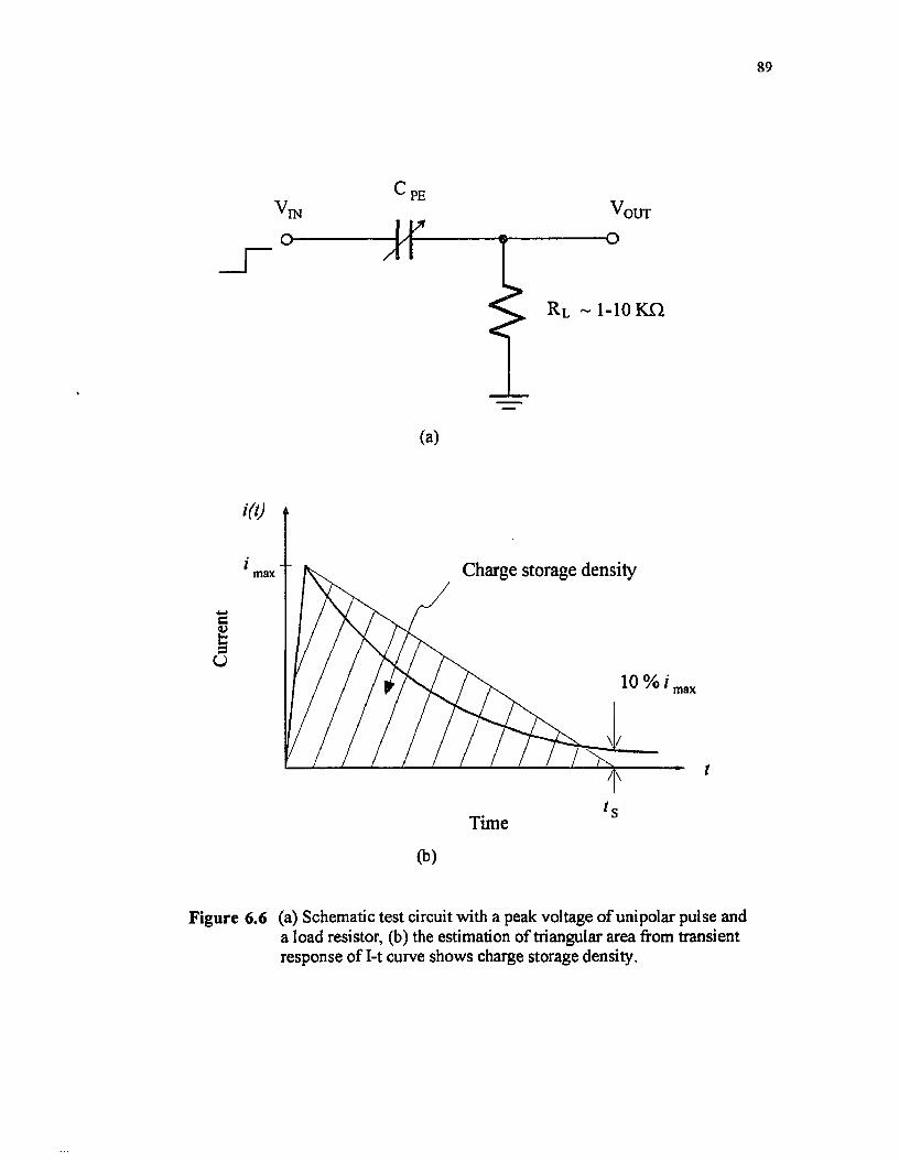
89
PEOUT
(a)
c<uS
U
m
Charge storage densitymax
10 % / max
Time
(b)
Figure 6.6 (a) Schematic test circuit with a peak voltage of unipolar pulse and a load resistor, (b) the estimation of triangular area from transient response of I-t curve shows charge storage density.
where, Vmax is the maximum response voltage,
Rl is the load resistance, and
A is the area of the paraelectric MDM capacitor.
The transient response is nearly exponential as shown in Figure 6.6 (b).
Figure B.7 presents the voltage-time curves with the different peak voltage of the
unipolar pulse experiments for the estimation of charge storage density and charging time.
The triangular area (i.e., charge storage density) is also increased, as the peak voltage of
unipolar pulse increases. The detailed results, compared with the data of P-E
measurements, are summarized in Table 6.1. It is noted that the charge storage density is
11.3 pC/cm2 at 4 V (200KV/cm) peak voltages. The charge storage density estimated by
the above equation produces an inaccuracy of about 9.7 % by comparison with the P-E
characteristics. The charging and discharging times are an important parameter in
determining the speed of a MDM capacitor in a DRAM unit cell. The total charging time
(tT) of the capacitors using paraelectric PLT thin films is expressed by:
tT = t c + t p — 2.303{RLCejgr ) + t p
where, Ctff - £'£° ^ E -,
and tp is the time of parasitic capacitance due to test setup. Lee et al [40] reported that
tp was estimated to be 0.7 psec for a capacitor area of 10000 pm2. The charging and
discharging times are dependent significantly on the electrode area, so that the switching

91
3coCDlaCDJZ
Coco•craO.£oo
c4J£uu=3C/3cd0/
x>*o0>td
3*3o
C/3 +J C C
■° ECD (DOP
C/32 o €3<135/1 ECD ,oo uj« Cu,f= £Vj O
VO4i
303
H
JOCD
wIeu
o
C l
•4a*
CCOtocoooc4-*CD4J«3
<5
2 ^ C <N 03 C73 s
I Io
eo4a*COCooO
•noCD"a3Q
c ^CD E "O .oCD ( J£P 3. £3 w J=
CJ>
o•c ECDu» -a4-*B ^ > 53 £
CD^ op ^ed cd 0) X! ^Oc o w
m(Sr-»
oor~-VO
ooo>n
csrW
ov d
C l©
Ovr~- oo p» vo rfr- vooof*5vo
OvOvm
© ov m00 in •—I
in vO 00* *—•
vo t s~ ro
OinOo Oin oors
oinrs
<N m i n

92
time decreases with a decrease o f the electrode area. Larsen et al [95] reported that it was
difficult to take measurements for the small capacitor area o f a MDM capacitor due to the
above-mentioned parasitic capacitance as well as the limitation of the measuring system's
respond time.
Figure B.8 shows the switching time response characteristics as a function of load
resistance under the same peak voltage of 4 V (200 KV/cm). The smaller the load
resistance, the faster the switching time response as shown in this Figure. The transient
response is governed by the following:
/(/) = / , exp
where, tT = 2.303RLCeff +tP and Ip is the maximum current. The switching time response
in Figure B.8 appears to correspond to the above equation.
CHAPTER 7
SUMMARY AND CONCLUSIONS
7.1 Summary
Since thin film material with extremely high dielectric constant was required in high
density capacitor of ULSI DRAM cell, lanthanum modified lead titanate (PLT; Pbj_x
LaxTii.x/403) thin films prepared by various deposition techniques have been
concentrated as an attractive candidate. In this research, paraelectric PLT thin films were
fabricated in a unique way by reactive magnetron sputtering system using a multi-
component metal target which was designed in our laboratory. The content of Pb in the
sputtering target appeared to play an important role in the film growth. As-deposited PLT
thin films were annealed to cause crystallization into paraelectric perovskite structure at
temperatures ranging from 550 to 750 °C.
The chemical composition, crystalline structure and surface morphology of the
films were extensively investigated. The semi quantitative analysis of stoichiometric
composition, based on RBS data for a standard PLT film, were measured by AES. The
best stoichiometric composition observed by AES analysis was Pb, 0.73; La, 0.28; Ti,
0.88; and O, 2.9. The relations of composition, crystalline structure and microstructure in
paraelectric PLT thin films annealed by a heat treatment appeared simultaneously
important from the results of XRD and SEM. The as-deposited films were altered during
post-deposition annealing by the inter-dependent relationship between composition and
crystalline structure through Pb evaporation.
The dielectric and electrical characteristics o f paraelectric perovskite PLT thin
films were conducted under different post-annealing conditions. The dielectric constant
increased significantly and the dissipation factor decreased slightly, as the post-annealing
temperature increased. The dielectric properties of PLT films were also exhibited as a
93

94
function of La content in the general formula of Pb-La-Ti-0 system. The dielectric
constant increased with a rise in La concentration. The best results of dielectric constant
and dissipation factor in the paraelectric capacitor, at low field measurement of 500 V/cm
(10 mV), were 1216 and 0.018, respectively. The measured dielectric constant was
tremendously different from the value of PLT bulk films reported by Hennings et al [22],
This is due to porosity and segregation phenomena caused by Pb evaporation in post
deposition annealing treatment.
The charge storage density (Qc) of the film annealed at 650 °C was 10.3 pC/cm2 at
the peak voltage of 4 V. The charge storage density at 750 °C was 12.5 pC/cm2, and then
the effective dielectric constant was about 706. The leakage current density was ordinarily
observed to decrease as the annealing temperature increased. But the leakage current for
PLT film annealed 750 °C was higher than that of the film heat-treated at 650 °C. The
optimal relationship between minimum leakage current density and maximum charge
storage density was chosen by the adjustable conditions of the post-annealing technique.
Voltage-time (V-t) measurement was also an important tool to determine the charge
storage density and the transient response of the paraelectric PLT capacitor. The charge
storage density was approximately 11.3 pC/cm2 at 4 V peak voltage. This estimated value
produced an inaccuracy of about 9.7 % in comparison with the value of P-E measurement.
The electrical characteristics of paraelectric PLT thin films for the capacitor dielectric of a
DRAM cell were compared in Table 7.1 with the results published by other researchers.
The results of dielectric constant and leakage current density in PLT films were generally
better than those of PZT films for ULSI DRAM applications. But it seemed that the
charge storage density of PLT and PZT thin films was somewhat less than the value
required in the planar capacitor of 1-T DRAM cell.
In summary, fabrication of the ternary compound PLT thin film could be easily
controlled by each metal element on the target. Post-annealing treatment should be
optimized as significant factors to improve the dielectric properties and electrical

Tabl
e 7.1
El
ectri
cal
Char
acte
ristic
s in
rece
nt r
esea
rche
s of
PT fam
ily
for D
RAM
appl
icat
ions
.
95
CM
t i l l3
13@
0.5M
V/c
m15
@0.
2MV
/cm
N.A
.
N.A
.
luo/AW
SZO©
III 15@
0.1M
V/c
m19
.6@
0.1M
V/c
m
81 42@
0.6M
V/c
m15
@0.
125M
V/c
m29
.3@
1.2M
V/c
m Eo §
o®
12.5
@0.
2MV
/cm
.*1=
3
N.A
.
0.1
@5M
V/c
mN
.A.
N.A
.
N.A
.
u»/Am
@
10 0.1
@0.
2MV
/cm
N.A
.
N.A
.
25@
2MV
/cm
0.5
@lM
V/c
mN
.A.
uw/A
WSZO
®10
1
to*
330
0.04
1500
0.01
513
000.
0280
00N
.A. £00
069 1300
N.A
.N
.A. 100
098
6100O
Sll 577
N.A
.N
.A.
820
0.2
1216
0.01
8
Thic
knes
sG
un)
0.25 0.5
0.35 0.4
0.4
0.2-
0.6
0.4
0.3-
1 00o1<No' 0.
2-0.
6
0.04
-0.1
5
1-3.
5
Mat
eria
l(L
a/Zr
)
H O>—1 (DA* — PLT
(28/
0)PL
T(2
8/0)
PLT
(0-4
2/0)
PLT
(25/
0)PZ
T(0
/50)
PZT
(0/6
5)PZ
T(0
/52)
PZT
(0/5
0-56
)PZ
T(0
/50)
PZT
(0/5
0)PZ
T(0
/52)
PLT
(28/
0)
Dep
ositi
on
MO
CV
D
Sol-G
el
MO
D
rf-M
ag.
Sput
ter
MO
D
Sol-G
el
dc-M
ag.
Sput
ter
KrF
Exci
mer
MIB
ERS
Sol-G
el
Sol-G
el
dc-M
ag.
Sput
ter
dc-M
ag.
Sput
ter
WmCG<D£<u
pS
Wata
nabe
(4
4)
1993
Dey
(30)
19
92Kh
an
(22)
19
92A
dach
i (1
) 19
91Sc
hwar
tz (4
1)
1991
Moa
zzam
i (3
8)
1992
Chik
aman
e (3
) 19
92Ro
y (1
5)
1992
Kru
pani
dhi
(8)
1992
Carra
no
(20)
19
91M
ader
ic (9
6)
1991
Sree
niva
s (6
2)
1988
NJI
T19
94

96
characteristics of the paraelectric capacitor. Thus, paraelectric perovskite PLT (28) thin
films offer critical advantages over the conventional dielectrics (e.g. silicon oxide, silicon
nitride and Z r02), and the ferroelectric thin films for ULSI DRAM applications.
7.2 Conclusions
The research showed that multi-component metal target sputtering was a promising
deposition technique to grow PLT thin films with the paraelectric perovskite structure.
The results of this investigation are described as follows.
(1) The paraelectric PLT thin films for the capacitor dielectric of DRAM memory
cells were successfully prepared by reactive magnetron sputtering using a multi-
component metal target. The individual control of each metal area on the sputtering target
had considerable influence on the stoichiometry and electrical properties of the thin films.
The relative ratio of each component area on the multi-component metal target was
estimated by the base on the chemical composition of the deposited thin films, the
sputtering yields for Pb, La and Ti metals and sticking coefficient in substrate.
(2) A post-deposition annealing treatment for the as-deposited PLT thin films
affected composition, crystalline structure and surface morphology due to Pb evaporation.
Single crystal film at 650 °C were smooth and the PLT thin films annealed at high
temperature (750 °C) frequently exhibited segregation phenomenon along the grain
boundary on the film surface. Finally, the annealing treatment for a prolonged period of
high temperature led to the formation of serious microcrack and craters.
(3) The dielectric characteristics were essentially dependent on the changes in the
chemical composition and crystalline phase with variation o f annealing heat treatment.
The dielectric constant increased significantly and the dissipation factor decreased slightly,
as the post-annealing temperature increased. The dielectric constant also increased with a
rise in La concentration. The best results of dielectric constant and dissipation factor in
the paraelectric PLT film annealed at 750 °C were 1216 and 0.018, respectively.

97
(4) The best value of the charge storage density in the 200 nm PLT (28) thin film
annealed at 750 °C was approximately 12.5 pC/cm2, and the effective dielectric constant
was about 706. The P-E plot at low electric field was similar with the linear behavior of a
normal dielectric material, while P-E characteristics were developed to the paraelectric
state of nonlinear behavior at high electric field.
(5) The leakage current density in the paraelectric PLT thin film annealed at 650°C
was around 0.1 pA/cm2 at the electric field of 0.25 MV/cm. The charge storage density
by V-t measurement was about 11.3 pC/cm2 at 4 V peak voltage. This estimated value
produced an inaccuracy of around 9.7 % in comparison with the value of P-E
measurement.
From the above results, the dielectric constant and charge storage density o f paraelectric
PLT thin films annealed at 750 °C were higher than those of the PLT films annealed at
650 °C. The leakage current density of the films annealed at 750 °C was worse value than
that of the films annealed at 650 °C. Therefore, the optimization among maximum
dielectric constant, maximum charge storage density and minimum leakage current density
for the capacitor dielectric of a DRAM cell was essentially adjusted by the conditions of
the post-deposition annealing treatment.
In conclusion, a large charge storage density, high dielectric constant and relatively
low leakage current density have been illustrated in the paraelectric perovskite PLT thin
films annealed under optimal conditions of post-deposition annealing treatment.
Therefore, it is expected that the paraelectric PLT capacitor is an attractive candidate for
potential application as capacitor dielectrics in ULSI DRAM cells.

APPENDIX A
TEST RESULTS OF PLT THIN FILM ANALYSIS
Oin
m§•■h
o£
o 00
SJJ!P'3*G)N
98
Figu
re
A.1
Auge
r ele
ctron
sp
ectro
scop
y sp
ectru
m of
pure
Pb
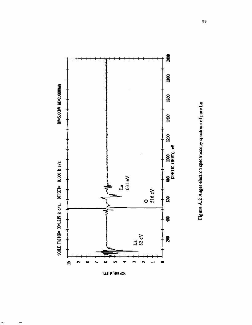
SCAL
E FA
CTOR
= 30
4.215
k
c/s.
0F
FSET
= 8.6
80
k c/s
BV
=5.60
kV
BI=
8.68
00uA
99
« <N •J OO
46 LO
£JJIP'3*G)N
Figu
re A
.2 Au
ger
electr
on
spec
trosco
py
spectr
um
of pu
re La

SCALE
FACTOR=
380.565
k c/s,
OFFSCT=
0.000
k c/s
BV=5.G
0kV BI=8.OO00uA
100
P ^
CD
£JJ!P'3*G)N
Figu
re
A.3
Auge
r ele
ctron
sp
ectr
osco
py
spect
rum
of pu
re Ti
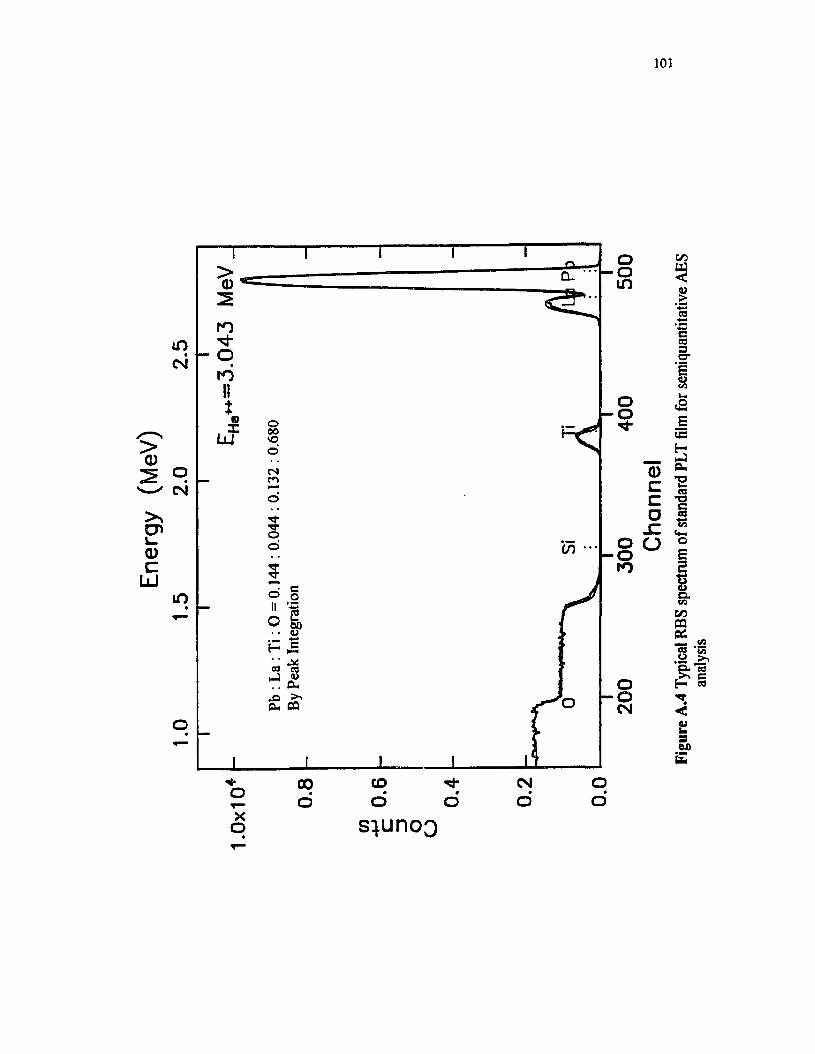
Ener
gy
(MeV
)
101
oovoo'
LlI
Ocsi o
oo'
in
o
00 to ^ N o2 o o d d d o S}UnoQ
200
300
400
500
Cha
nnel
Figu
re
A.4
Typi
cal
RBS
spec
trum
of sta
ndar
d PL
T film
for
sem
iqua
ntita
tive
AES

102
(N<*1?
Ovf?»• v~i . . — -S >0 Nf V" - m N ^
O
VOCNVOu
1£
<NJ00
mONUJ
oo 00 N . CslCO
tr>
SJJIP'3s(3)H
Figu
re
A.5
Typi
cal
AES
spec
trum
of sta
ndar
d PL
T fil
m

103
vO•"T
5h
i1Cm9)d
6U<sUJI
inm —•Ov Ov
<N00
oo_ fN <*) • m 00 O
S s i ivo (Sft o o ft 7
« oS n —■ n J H0 ,2" ■a-- «
X « O. hJ P o £
>Vvo<N <uVO ,— 1
tn
in>o>00rf
><umov
CO i n
SJJ!P*Jt(3)M
Figu
re
A.6
Typi
cal
resu
lts o
f AE
S an
alysis
on
an as
-dep
osite
d PL
T fil
m

SCAL
E FA
CTOR
= 92
.888
k
c/s,
OF
FSET
= 0.0
00
k c/
s BV
=5.0O
kV
BI=0
.OOO
OuA
104
oo00
00
t" ° w . iri *' rr w oo oo n— (N
- „ wO n ._ -
fs r .■» " i j Ht- -i 2 cs CO
r f s f J d ejo Cd . _ x>a J h O ' d .
« ’
00
CO CDO 00
«3
£JJ!P'3»G)N
Figu
re
A.7
AES
spec
trum
of PL
T (2
8) t
hin
films
with
di
ffere
nt t
arge
t ar
ea:
(a) P
b : L
a :T
i =
8.38
: 5.
85:
85.7
6(b)
Pb
: La
: Ti
= 7.6
0 : 7
.80
: 84.
60

o00I Noo rrr~ o oo oo
cK ^ °® v d — — oo r-« N ifl - (NO
tsso
oo
Os
o00 C \Jo CO
SJJ!P'3«<3)H

106
T
v§
00VO
cu
cu
e e ooo
o -5
X *3 -V
Figu
re A
.8 Au
ger
depth
pr
ofile
of
an as
-dep
osite
d PL
T film
as
a fu
nctio
n of
etchin
g tim
e

107
«
s cu>
oo00o'
CN
oo ocn o ooooo
C89>
<U00CO
C£
&
cfiE o o •S N UtC • •00 00 00 c n • • • •w U-1 OE— oo oo J w KCU . . . .“o 0 0 o® r«l vo" oo K tc o II II 5 .£—• H 1
8 - 2 j• o • • • •
c-m J D « C« ,£ o«00
<! - 9v<£s00
CD X )
X '3 'V

108
I
1
cu
cu
m
Ocu cu00
CN©
CN
o o oo oo
X - a ‘ V

Ener
gy
(MeV
)
109
inCM
Ll I
00
o
OCMCO
in
<Dcco
S Ioto
CM
XCM s ^ u n o Q
Figu
re A
.10
Ruth
erfo
rd
back
scat
terin
g sp
ectra
of
PLT
thin
films
with
di
ffere
nt a
rea
ratio
of
mul
ti-co
mpo
nent
meta
l ta
rget

Ener
gy
(MeV
)
110
inCN
LU
OCN oo
©0-1(N
ts v> I"; t/1 O O
II O' II
O*in
o t
oo
CD
m
oon
CN
XCN S } u n o Q
Cha
nnel

Ener
gy
(MeV
)2.0
2.
5
in
UJ
OvOO o
o ^ cm •2 r- -33 t'-« m 2 6m n
C 11 E 11 SPH 8 P
m
q
oooCN
in
ooro
ooCN
s^ L in o Q
Cha
nnel

112
incvi
m
><D
2
cna>c
Ld
vO(S
1 . tfl <N 2 ii Q*
oO
CD ^ CN
s}unoQ
200
300
400
500
Cha
nnel

113
(Oil)
(001)
X )
a
:B
■B
-9
H
-»
:r i
UoO«n
E-a
t-s
R
H
uoOinlOo
Figu
re A
.ll X
RD
patte
rns
of PL
T thi
n fil
ms w
ith
diffe
rent
pos
t-ann
ealin
g tre
atm
ent.
Thes
e PL
T fil
ms b
elong
to
the
type
D in
Table
5.
3

114
Sub.
( 110)
(100) (211)
_ ^ / l(c) 650 °C
(210)
(b) 550 °C
(a) As-dep.
6050403020
TWO THETA
Figure A. 12 XRD spectra of the paraelectric PLT (28) thin films as a function of post- annealing temperature. These PLT films belong to the type A in Table 5.3

115
750 °C
650 °C
550 °C
TWO THETA
Figure A.13 XRD step scans to observe the (211) peak shift of PLT (28) films at 550, 650, and 750 °C for 5 min

116
Sub.
(110)750 °C
( 100)(200)
(211)
J L650 °C
550 °C
PbO
40 6020 30 50
TWO THETA
Figure A.14 XRD patterns as a function of annealing temperature for PLT thin films of chemical composition type B in Table 5.3

117
750 °CMgO( 100)
(200)
550 °C
As-dep.
20 40 50 6030
TWO THETA
Figure A.15XRD spectra of PLT thin films on single-crystal MgO (100) substrate

INTE
NSIT
Y
118
Sub.(200)
60 min.
( 110)( 100 )
(211)
30 min.
10 min.
As-dep.
6050403020
TWO THETA
Figure A. 16 XRD patterns of the paraelectric PLT (28) thin films as a function of annealing time at 650 °C

Figure A. 17 Typical SEM of as-deposited PLT film with smooth surface
Figure A.18Tvpicai SEM of PLT thin film annealed at 650 °C for 5 min

120
- 'jap*; v ' 7
v '> 'j& fT,/x ^ '^ ^ v c k y . ■
Wt-1. '
Figure A.19 Segregation of grain boundary in PLT films due to Pb evaporation

121
Microcrack
Figure A.20 SEM of typical defects on PLT films annealed at 750 °C for 60 min:(a) crack and (b) craters and holes

APPENDIX B
TEST RESULTS OF ELECTRICAL ANALYSIS
X: 100 KV/cm/Div.Y: 10.94 |aC/cm2/Div. ................ ....... ;....- ......-............ ;............C0: 68.7 nF
........................ -............ :............ -............ ............-........-.. .......................-...............
(a)V p = l V
X: 100 KV/cm/Div.Y: 10.94 (iC/cn^/Div. ................r............ : -.... .....1......- -------------C0: 68.7 nF
............. -......... . - ... '........... .........
(b) Vp = 2 V
X: 100 KV/cm/Drv. Y: 10.94 fiC/cm^/Div. Cn: 68.7 nF
(c) Vp = 4 V
Figure B.l P-E characteristics as a function of peak voltage for 200 ran PLT (28) thin film at 650 °C for 5 min
122

123
X: 100 KV/cm/Div. Y: 10.94 fiC/cm2/Div.C0: 68.7 nF
(a)VD= l V
X: 100 KV/cm/Div. Y: 10.94 |iC/cm2/Div, C„: 68.7 nF
X: 100 KV/cm/Div. Y: 10.94 fiC/cm2/Div Cn: 68.7 nF
Figure B.2 P-H characteristics with different peak voltages for 200 nm PLT (28) thin film at 750 °C for 5 min

124
X: 100 KV/cm/Div.Y: 10.94 |iC/cm2/Div. ... C„: 68.7 nF
(a) 550 °C
X: 100 KV/cm/Div. Y: 10.94 |tC/cm2/Div. Cft: 68.7 nF
(b) 650 °C
X: 100 KV/cm/Div. Y: 10.94 (j.C/cm2/Div. C„: 68.7 nF
(c) 750 °C
Figure B.3 P-E characteristics as a function of annealing temperature for PLT films at the same peak voltage of 4 V (200 KV/cm)

125
<o©
o00 O'©
©<n
©©
eo
s2’a3«3o
2ajW
©</■>
[_uio/V] Xjisuap juaimo
Figur
e B
.4I-V
plo
t of
PLT
thin
films
with
di
ffere
nt p
ost-a
nnea
ling
tem
pera
ture
for
5 m
in.

126
Oo
•ri
C CO
cuor lQ
u_ a)n Fi
gure
B.S
Th
e ph
enom
ena
of dc
volta
ge-in
duce
d re
sistan
ce
degr
adat
ion
sudd
enly
ris
ing
in the
lea
kage
cu
rrent
lev
el pr
ior t
o di
electr
ic br
eakd
own
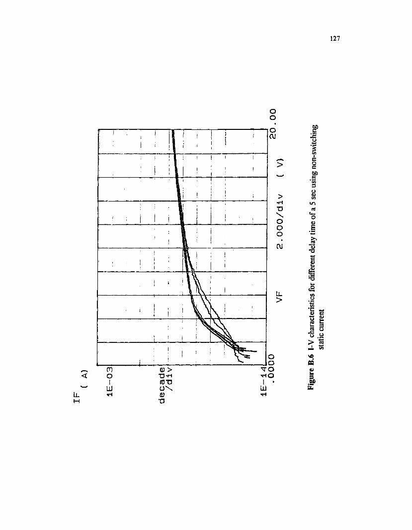
127
OO
m (D > r r o< o ■D-rt ^iO
i (0*0 i •LU ui
Ll a)M TJ
igur
e B
.6 I-V
ch
arac
teris
tics
for d
iffer
ent
delay
tim
e of
a 5
sec
using
no
n-sw
itchi
ng
static
cu
rren
t

128
X: 1 jisec/Div. Vp = l VY: 1 V/Div.Rl : 1 K Q
4v
i
X: 1 fxsec/Div. Vp = 2 VY: 1 V/Div.Rl : I K n »
X: 1 usec/Div. v D = 3 VY: 1 V/Div. PRl : 1 K Q r
X: 1 ^sec/Div. Vp = 4 VY: 1 V/Div.R , : 1 K Q
Y: 1 V/Div. R l : 1 KD.
a L . x! V
X: 1 iisec/Div. y = 5 Vi P
Figure B.7 Voltage-time characteristics of PLT (28) MDM capacitors with different peak voltage of unipolar pulse

129
X: 2 jisec/Div. ,Y: 1 V/Div. E V p = 4 VRl : 10 K n
X: 1 jisec/Div.Y: 1 V/Div. V p = 4 VRL: 1 KH %
X: 0.5 fisec/Div. _Y: 1 V/Div. v p = 4 vRl : 0.5 K D
Figure B.8 Switching time response characteristics as a function of load resistance under the same peak voltage of 4 V (200 KV/cm)

REFERENCES
[1] H. Adachi and K. Wasa. "Sputtering Preparation of Ferroelectric PLZT Thin Films and Their Optical Application." DEEE Trans. Ultra. Ferro. Freq. Control, 38(6), 645,1991.
[2] R. Takayama, Y. Tomita, K. Iijima, and I. Ueda. "Preparation and Characteristics of Pyroelectric Infrared Sensors Made of c-axis Oriented La-Modified PbTi03 Thin Films." J. Appl. Phys. 61(1), 411, 1987.
[3] V. Chikarmane, J. Kim, C. Sudhama, J. Lee, A. Tasch, and S. Novak. "Annealing of PZT (65/35) Thin Films for ULSI Storage Dielectric Applications: Phase Transformation and Electrical Characteristics." J. Elect. Mater. 21(5), 503, 1992.
[4] L. Wang, A. Pignolet, and F. Levy. "Properties of PZT Thin Films Prepared by rf Magnetron Sputtering and Heat Treatment." Mater. Res. Bull. 25, 1495, 1990.
[5] M. Okuyama, and Y. Hamakawa. "PT Ferroelectric Thin Films and Their Pyroelectric Application." Ferro. 118, 261, 1991.
[6] R. Watton, and M. Todd. "Induced Pyroelectricity in Sputtered PST Films and Their Merit for IR Detector Arrays." Ferro. 118, 279, 1991.
[7] R. Castelland, and L.Feinstein. "Ion-Beam Deposition of Thin Films of Ferroelectric PZT." J. Appl. Phys. 50, 4406, 1979.
[8] B. Krupanidhi, H. Hu, and V. Kumar. "Multi-Ion-Beam Reactive Sputter Deposition of Ferroelectric PZT Thin Films." J. Appl. Phys. 71, 376, 1992.
[9] M. Okada, S. Takai, M. Amemiya, and K. Tominaga. "Preparation of c-axis Oriented PbTi03 Thin Films by MOCVD under Reduced Pressure." Jpn. J. Appl. Phys. 28, 1030, 1989.
[10] R. Vest. "Metallo-Organic Decomposition Processing of Ferroelectric and Electro- Optic Films: A Review." Ferro. 102, 53, 1990.
[11] G. Haertling. "Ferroelectric Thin Films for Electronic Applications." J. Vac. Sci. Technol. 9(3 A), 414, 1991.
[12] S. Dey, and R.Zuleeg. "Integrated Sol-Gel PZT Thin Films on Pt, Si and GaAs for Non-volatile Memory Applications," Ferro. 108, 37, 1990.
130

131
REFERENCES(Continued)
[13] G. Spierings, M. Ulenaers, G. kampschoer, H. Hal, and P. Larsen. "Preparation and Ferroelectric Properties of PZT (53/47) Thin Films by Spin Coating and Metalorganic Decomposition." J. Appl. Phys. 70, 2290, 1991.
[14] H. Buhay, S. Sinharoy, W. Kasner, M. Francombe, D. Lampe, and E. Stepke."Pulsed Laser Deposition and Ferroelectric Characterization of Bismuth Titanate Films." Appl. Phys. Lett. 58, 1470, 1991.
[15] D. Roy, S. Krupanidhi, and J. Dougherty. "Excimer Laser Ablation of Ferroelectric PZT Thin Films with Low Pressure Direct-Current Glow Discharge." J. Vac. Sci. Technol. 10(4A), 1827, 1992.
[16] M. Lines, and A. Glass. Principles and Applications o f Ferroelectrics and Related Materials. Clarendon Press, Oxford, 1977.
[17] C. Land, P. Thacher, and G. Haertling. Electrooptic Ceramics, in Applied Solid State Science: Vol 4 edited by R.Wolfe, Academic Press, New York, P137, 1974.
[18] H. Adachi, T. Kawaguchi, K. Setsune, K. Ohji, and K. Wasa. "Electro-Optic Effects of PLZT Thin Films Prepared by rf Planar Magnetron Sputtering." Appl. Phys. Lett. 42(10), 867, 1983.
[19] G. Haertling. Piezoelectric and Electrooptic Ceramics, in Ceramic Materials for Electronics edited by R.Buchanan, 2nd Edition, Marcel Dekker, Inc., New York,PI 29, 1991.
[20] J. Carrano, C. Sudhama, V. Chikarmane, J. Lee, A. Tasch, W. Shepherd, and N. Abt. "Electrical and Reliability Properties of PZT Thin Films for ULSI DRAM Applications." IEEE Ultra. Ferro. Freq. Control 38(6), 690, 1991.
[21] D. Hennings, and K. Hardtl. "The Distribution of Vacancies in Lanthana-Doped Lead Titanate." Phys. Stat. Sol. (a) 3, 465, 1970.
[22] A. Khan, I. Yoo, and S. Desu. "Preparation and Characterization of PLT Thin Films by Metalorganic Decomposition." IEEE-92, ISAF, 412, 1992.
[23] D. Hennings. "The Range of Existence of Perovskite Phase in the System PbO-Ti02- La20 3." Mater. Res. Bull. 6, 329, 1971.

132
REFERENCES(Continued)
[24] K. Keizer, and A. Burggraaf. "Grain Size Effects on the Ferroelectric-Paraelectric Transition, the Dielectric Constant, and the Lattice Parameters in Lanthana- Substituted Lead Titanate." Phys. Stat. Sol. (a) 26, 561, 1974.
[25] R. Roth, T. Negas, and L. Cook. Phase Diagrams fo r Ceramists: Vo! 4. The American Ceramic Society, Inc., Ohio, P223, 1981.
[26] G. Fox, S. Krupanidhi, K. More, and L. Allard. "Composition/Structure/Property Relations of Multi-Ion-Beam Reactive Sputtered Lead Lanthanum Titanate Thin Films: Part I. Composition and Structure Analysis." J. Mater. Res. 7(11), 3039,1992.
[27] J. Thornton. "Influence of Substrate Temperature and Deposition Rate on Structure of Thick Sputtered Cu Coatings." J. Vac. Sci. Technol. 12(4), 830, 1975,
[28] T. Yamamoto, H. Igarashi, and K. Okazaki. "Dielectric, Electro-mechanical, Optical, and Mechanical Properties of Lanthana-Modified Lead Titanate Ceramics." J. Amer. Ceram. Soc. 66(5), 363, 1983.
[29] K. Keizer, G. Lansink, and A. Burggraaf. "Anomalous Dielectric Behaviour of La(III) Substituted Lead Titanate Ceramics." J. Phys. Chem. Sol. 39, 59, 1978.
[30] S. Dey, and J.Lee. "Cubic Paraelectric (Nonferroelectric) Perovskite PLT Thin Films with High Permittivity for ULSI DRAMs and Decoupling Capacitors." IEEE Elect. Dev. 39(7), 1607, 1992.
[31] L. Parker, and A. Tasch. "Ferroelectric Materials for 64 and 256 Mb DRAMs."IEEE Circuit Dev. Mag. 17, Jan. 1990.
[32] A. Tasch. "Storage Capacitor Dielectric Issues and Requirements in Gigabit One- Transistor Cell MOS RAMs." 184th Electrochem. Soc. Meeting, New Orleans,P238, 1993.
[33] R. Dennard. "Field-Effect Transistor Memory." US Patent 3 387 286, June 4, 1968.
[34] D. Bondurant. "Ferroelectric RAM memory Family for Critical Data Storage." Ferro. 112, 273, 1990.
[35] S. Dey, and R. Zuleeg. "Processing and Parameters of Sol-Gel PZT Thin Films for GaAs Memory Applications." Ferro. 112, 309, 1990.

133
REFERENCES(Continued)
[36] C. Hashimoto, H. Oikawa, and N. Honma. 11 Leakage-Current Reduction in Thin Ta20 5 Films for High Density VLSI Memories." IEEE Elect. Dev. 36(1), 14, 1989.
[37] L. Manchanda, and M. Gurvitch. "Yttrium Oxide/Silicon Dioxide: A New Dielectric Structure for VLSI/ULSI Circuits." IEEE Elect. Dev. Lett. 9(4), 180.1988.
[38] R. Moazzami, C. Hu, and W. Shepherd. "Electrical Characteristics o f Ferroelectric PZT Thin Films for DRAM Applications." IEEE Elect. Dev. 39(9), 2044, 1992.
[39] R. Moazzami, C. Hu, and W. Shepherd. "A Ferroelectric DRAM Cell for High Density NVRAM." IEEE Elect. Dev. Lett. 11(10), 454, 1990.
[40] J. Lee, and S. Dey. "Sol-Gel Derived PLT Thin Films with High Linear Permittivity for ULSI DRAMs." Ceram. Trans. 25, 235, 1992.
[41] A. Tasch, and L. Parker. "Memory Cell and technology Issues for 64- and 256-Mbit One-Transistor Cell MOS DRAMs." Proc. IEEE 77(3), 374, 1989.
[42] H. Adachi, T. Mitsuya, O. Yamazaki, and K. Wasa. "Ferroelectric PLZT Epitaxial Thin Films on Sapphire Grown by rf planar Magnetron Sputtering." J. Appl. Phys. 60(2), 736, 1986.
[43] R. Schwartz, B. Tuttle, D. Doughty, C. Land, D. Goodnow, C. Hernandez, T. Zender, and S. Martinez. "Preparation and Characterization of Chemically Derived PLT Thin Films." IEEE Ultra. Ferro. Freq. Control, 38(6), 677, 1991.
[44] S. Watanabe, T. Fujiu, and A. Tanaka. "Lanthanum-Modified Lead Titanate Thin Film Formed by Low Temperature Chemical Vapor Deposition and Subsequent Annealing." Appl. Phys. Lett. 62(25), 3377, 1993.
[45] Z. Qian, D. Xiao, J. Zhu, and Z. Li. "X-ray Photoelectron Spectroscopy and Auger Electron Spectroscopy Studies of Ferroelectric PLT Thin Films Prepared by A Multi- Ion-Beam Reactive Cosputtering Technique." J. Appl. Phys. 74(1), 224, 1993.
[46] G. Fox, S. Krupanidhi, and K. More. "Composition/Structure/Property Relations of Multi-Ion-Beam Reactive Sputtered Lead Lanthanum Titanate Thin Films: Part II. Textured Microstructure Development." J. Mater. Res. 8(9), 2191, 1993.
[47] S. Krupanidhi. "Recent Advances in Physical Vapor Growth Processes for Ferroelectric Thin Films." J. Vac. Sci. Technol. 10(4A), 1569, 1992.

134
REFERENCES(Continued)
[48] S. Swan. "Magnetron Sputtering." Phys. Technol. 19, 67, 1988.
[49] R. Waits. Planar Magnetron Sputtering, in Thin Film Processes edited by J.Vossen and W.Kem, Academic Press, New York, P131, 1978.
[50] Hexetch 640, Asymmetrical Reactive Ion Etch System. Instruction Manual, Plasma- Therm, Inc., Kresson, NJ, 1982.
[51] Tri-Mag Sputtering Source. 383-BPM-FS-AS-VCOS. Instruction Manual, L.M.Simard Inc., Oregon, 1989.
[52] The Simion PC/PS2, User's Manual, Version 4.0, Idaho National Engineering Laboratory, EG&G Idaho Inc., Idaho Falls, Idaho, 1988.
[53] B. Chapman. Glow Discharge Processes: Sputtering and Plasma Etching. John Wiley and Sons, New York, P263, 1980.
[54] F. Green, and B. Chapman. "Electron Effects in Magnetron Sputtering." J. Vac. Sci. Technol. 13(1), 165, 1976.
[55] A. Kingon, H. Al-Shareef, and S. Summerfelt. "Electrodes Systems for Ferroelectric Capacitor Structures in DRAMs." 184th Eiectrochem. Soc. Meeting, New Orleans, P263, 1993.
[56] K. Sreenivas, I. Reaney, T. Maeder, N. Setter, C. Jagadish, and R. Elliman. "Investigation of Pt/Ti Bilayer Metallization on Silicon for Ferroelectric Thin Film Integration." J. Appl. Phys. 75(1), 232, 1994.
[57] I. Kondo, T. Yoneyama, O. Takenaka, and A. Kinbara. "Formation of High Adhesive and Pure Pt Layers on Ti02." J. Vac. Sci. Technol. 10(6A), 3456, 1992.
[58] J. Olowolafe, R. Jones, A. Campbell, R. Hegde, C. Mogab, and R. Gregogy. "Effects of Anneal Ambients and Pt Thickness on Pt/Ti and Pt/Ti/TiN Interfacial Reactions."J. Appl. Phys. 73(4), 1764, 1993.
[59] A. Croteau, and M. Sayer. "Growth and Characterization of PZT Films Deposited by Reactive Sputtering of Metallic Targets." IEEE-86, ISAF, 606, 1986.

135
REFERENCES(Continued)
[60] T. Yamamoto, T. Imai, and T. Shiozaki. "Preparation of PZT Thin Films by Reactive rf Magnetron Cosputtering Using Multi-Element Metallic Targets and Their Evaluations." IEEE-92, ISAF, 317, 1992.
[61] M. Sayer. "Fabrication and Application of Multi-Component Piezoelectric Thin Films." IEEE-86, ISAF, 560, 1986.
[62] K. Sreenivas, and M. Sayer. "Characterization of PZT Thin Films Deposited from Multi-Element Metal Targets." J. Appl. Phys. 64(3), 1484, 1988.
[63] Y. Ochiai, K. Aso, M. Hayakawa, H. Matsuda, K. Hayash, W. Ishikawa, and Y. Iwasaki. "On Specimen Preparation by rf Planar Magnetron Sputtering." J. Vac. Sci. Technol. 4(1 A), 19, 1986.
[64] T. Fukami, and T. Sakuma. "Composition of Reactively Sputtered PLZT Films." Jpn. J. Appl. Phys. 20(8), 1599, 1981.
[65] T. Hase, and T. Shiosaki. "Preparation and Switching Kinetics of PZT Thin Films Deposited by Reactive Sputtering." Jpn. J. Appl. Phys. 30(9B), 2159, 1991.
[66] P. Sigmund. "Theory of Sputtering. I. Sputtering Yield of Amorphous and Polycrystalline Targets." Phys. Rev. 184(2), 3883, 1969.
[67] P. Sigmund. "Sputtering of Single and Multiple Component Materials." J. Vac. Sci. Technol. 17(1), 396, 1980.
[68] H. Adachi, T. Mitsuyu, O. Yamazaki, and K. Wasa. "Preparation and Properties of PLT Epitaxial Thin Films by Multi-Target Sputtering." Jpn. J. Appl. Phys. Suppl. 24(3), 13, 1985.
[69] R. Comely. Film Growth by Ion Beam and Plasma Discharge Sputtering Method, in Ion Beam Assisted Film Growth edited by T.Itoh. Japan. P9, 1989.
[70] O. Auciello, and A. Kingon. "A Critical Review of Physical Vapor Deposition Techniques for the Synthesis of Ferroelectric Thin Films." IEEE-92, ISAF, 320,1992.
[71] H. Adachi, K. Hirochi, K. Setsune, M. Kitabatake, and K. Wasa. "Low Temperature Process for the Preparation of High Tc Superconducting Thin Films." Appl. Phys. Lett. 51(26), 2263, 1987.
136
REFERENCES(Continued)
[72] R. Sandstrom, W. Gallagher, T. Dinger, R. Koch, R. Laibowitz, A. Kleinsasser,R. Gambino, B. Bumble, and M. Chisholm. "Reliable Single-Target Sputtering Process for High Temperature Superconducting Films and Devices." Appl. Phys. Lett. 53(5), 444, 1988.
[73] N. Terada, H. Ihara, M. Jo, M. Hirabayashi, Y. Kimura, K. Matsutani, K. Hirata, E. Ohno, R. Sugise, and F. Gawashima. "Sputter Synthesis of YBCO As-Deposited Superconducting Thin Films from Stoichiometric Target: A Mechanism of Compositional Deviation and Its Control." Jpn. J. Appl. Phys. 27(4), L639, 1988.
[74] M. Okuyama, T. Ueda, and Y. Hamakawa. "Bias Effect in rf Sputtering ofPbTi03 Thin Films." Proc. 1985 5th Meeting on Ferro, and Their Appl., Kyoto, 1985.
[75] R. Hill. Physical Vapor Deposition, Temescal, Berkeley, P57, 1976.
[76] J. Vossen, and J. Cuomo. Glow Discharge Sputter Deposition, in Thin Film Processes edited by J. Vossen and W.Kem, Academic Press, New York, P48, 1978.
[77] V. Fridkin. Ferroelectric Semiconductors. Consultants Bureau, New York, P70, 1980.
[78] Z. Surowiak, J. Dudek, Y. Goltzov, S. Gach, A. Dranishnikov, L. Shpak, andV. Yurkevich. "The Semiconductor Properties on the System Metal-Semiconductive Ferroelectric-Metal." Ferro. 123, 19, 1991.
[79] L. Davis, N. MacDonald, P: Palmberg, G. Riach, and R. Weber. Handbook o f Auger Electron Spectroscopy. Physical Electronics Industries, Eden Prairie, Minn. 1976.
[80] C. Chang. "Auger Electron Spectroscopy." Surf. Sci. 25, 53, 1991.
[81] Y. Shimizu, K. Udayakumar, and L. Cross. "Preparation and Electron Properties of Lanthanum-Doped Lead Titanate Thin Films by Sol-Gel Processing." J. Amer. Ceram. Soc. 74(12), 3023, 1991.
[82] G. Samara. "Pressure and Temperature Dependence of the Dielectric Properties and Phase Transitions of the Ferroelectric Perovskites: PbTi03 and BaTi03 " Ferro. 2, 277, 1971.
[83] S. Dana, K. Etzold, and J. Clabes. "Crystallization of Sol-Gel Derived Lead Zirconate Titanate Thin Films." J. Appl. Phys. 69(8), 4398, 1991.

137
REFERENCES(Continued)
[84] T. Ogawa, A. Senda, and T. Kasanami. "Controlling the Crystal Orientations of Lead Titanate Thin Films." Jpn. J. Appl. Phys. 30(9B), 2145, 1991.
[85] M. Murakami. "Thermal Strain in Lead Thin Films VI: Effects o f Oxygen Doping." Thin Sol. films, 69, 253, 1980.
[86] R. Opila. "The Role of Grain Boundaries in the Surface Segregation of TiN in TiN- Lead Alloys." J. Vac. Sci. Technol. 4(2A), 173, 1986.
[87] C. Sawyer, and C. Tower. "Rochelle Salt as a Piezoelectric." Phys. Rev. 35, 269, 1930 or Diamant, H., K. Drenck, and R. Pepinsky. "Bridge for Accurate Measurement of Ferroelectric Hystersis." Rev. Sci. Instru. 28(1), 30, 1957.
[88] G. Fox, and S. Krupanidhi. "Composition/Structure/Property Relations of Multi-Ion- Beam Reactive Sputtered Lead Lanthanum Titanate Thin Films: Part III. Electrical Properties." J. Mater. Res. 8(9), 2203, 1993.
[89] S. Sze. Physics o f Semiconductor Devices. 2th Edition, Wiley, NJ, P403, 1981.
[90] I. Yoo, and S. Desu. "Leakage Current Mechanism and Accelerated Unified Test of Lead Zirconate Titanate Thin Film Capacitor." IEEE-92, ISAF, 225, 1992.
[91] V. Chikarmane, C. Sudhama, J. Kim, J. Lee, A. Tasch, and S. Novak. "Effects of Post-Deposition Annealing Ambient on the Electrical Characteristics and Phase Transformation Kinetics of Sputtering Lead Zirconate Titanate (65/35) Thin Film Capacitors." J. Vac. Sci. Technol. 10(4A), 1562, 1992.
[92] R. Waser, T. Baiatu, and K. Hardtl. "dc Electrical Degradation of Perovskite-Type Titanate: I. Ceramics." J. Amer. Ceram. Soc. 73(6), 1645, 1990.
[93] T. Baiatu, R. Waser, and K. Hardtl. "dc Electrical Degradation of Perovskite-Type Titanate: III. A Model of the Mechanism." J. Amer. Ceram. Soc. 73(6), 1663, 1990.
[94] H. Duiker, P. Beale, J. Scott, C. Araujo, B. Melnick, J. Cuchiaro, and L. McMillan. "Fatigue and Switching in Ferroelectric Memories: Theory and Experiment." J. Appl. Phys. 68(11), 5783, 1990.

138
REFERENCES(Continued)
[95] P. Larsen, G. Kampschoer, M. Ulenaers, G. Spierings, and R. Cuppens. "Nanosecond Switching of Thin Ferroelectric Films." Appl. Phys. Lett. 59(5), 611, 1991.
[96] B. Maderic, L. Sanchez, and S. Wu. "Ferroelectric Switching, Memory Retention and Endurance Properties of Very Thin PZT Films." Ferro. 116, 65, 1991.