Embed Size (px)
Citation preview

Copyright
By
Muhammad Tauseef Rab
2013

The Dissertation Committee for Muhammad Tauseef Rab Certifies that this is the
approved version of the following dissertation:
Techniques To Minimize Circuitry and Improve Efficiency for
Defect Tolerance
Committee:
Nur A. Touba, Supervisor
Andreas Gerstlauer
David Z. Pan
Sarfraz Khurshid
Baker Mohammad

Techniques To Minimize Circuitry and Improve Efficiency for
Defect Tolerance
by
Muhammad Tauseef Rab, B.S.EE.; M.S.E.
Dissertation
Presented to the Faculty of the Graduate School of
The University of Texas at Austin
in Partial Fulfillment
of the Requirements
for the Degree of
DOCTOR OF PHILOSOPHY
The University of Texas at Austin
May 2013

Dedication
To my parents Dr Muhammad Fasih-ur-Rab and Dr Shahnaz Iffat.
To my wife Sameen Siddiqi and our daughter Sarah.
To my brother Muhammad Asim Rab.
To my entire family.

v
Acknowledgements
Alhumdu liLlah! All praises belong to Allah, the most merciful, for allowing me
to be able to complete this work.
This thesis is dedicated to my loving parents, who have always supported me in
everything and for their tireless efforts and continuous prayers at every stage of my life.
I am indebted to my advisor Dr Nur A Touba for his guidance, help and
invaluable mentorship throughout the PhD studies. Nur’s passion for the subject in
addition to his very pleasant personality makes him a great tutor, advisor and mentor. I
will consider myself successful if I am able to emulate him in my career.
I would like to thank my committee members Dr. Andreas Gerstlauer, Dr. David.
Z. Pan, Dr. Sarfraz Khurshid and in particular Dr. Baker Mohammad who was
instrumental in getting the best out of me.
I would like to thank all my friends and extended family who have been with me
through this very rewarding journey, in particular Abbas Hasan, Adnan Wasim, Bilal
Janjua, Hamid Tirmizi, Irfan Waheed, Aater Suleman, Kamil Fareed and Umar Farooq. I
would like to thank Amber Hasaan for providing me with assistance with coding key
algorithms. Asad Bawa deserves a special mention for spending countless brainstorming
hours with me on multiple occasions. I would also like to thank my parents-in-law for
their support and prayers.
I would like to thank the University of Texas at Austin for being the perfect
learning place which taught me a lot, from the day I entered in the BSEE program till

vi
today. In addition, I would like to thank Qualcomm Inc, for financially supporting my
studies.
This work would not have been possible if not for the academic coaching and
constant mentorship I got from my brother, Muhammad Asim Rab who has been a great
big brother throughout my life.
My wife, Sameen Siddiqi, has been the most important factor in the completion of
this thesis. It is because of her belief, prayers and support that this PhD could be
completed.
And finally, I would like to thank the most important member, without whose
cooperation and cheering, life would not be complete; Sarah, our beloved daughter.
Alhumdu liLah (all praises belong to Allah, Almighty)

vii
Techniques To Minimize Circuitry and Improve Efficiency for
Defect Tolerance
Muhammad Tauseef Rab, Ph.D.
The University of Texas at Austin, 2013
Supervisor: Nur. A. Touba
As technology continues to scale to smaller geometries and newer dimensions (3-
D), with increasingly complex manufacturing processes, the ability to reliably
manufacture 100% defect-free circuitry becomes a significant challenge. While
implementing additional circuitry to improve yield is economically justifiable, this thesis
addresses the cost of defect tolerance by providing lower cost solutions or alternatively
more defect tolerance for the same cost in state-of-the-art ICs, including three-
dimensional ICs (3-D ICs). Conventional defect tolerance techniques involve
incorporating redundancy into the design. This thesis introduces novel designs to
maximize the utility of spare elements with minimal circuitry overhead, thereby
improving the yield. One idea proposed is Selective Row Partitioning (SRP), a technique
which allows a single spare column to be used to repair multiple defective cells in
multiple columns. This is done by selectively decoding the row address bits when
generating the select signals for the column multiplexers. This logically segments the
spare column allowing it to replace different columns in different partitions of the row
address space. All the chips are identical, but fuses are used to customize the row
decoding circuitry on a chip-by-chip basis. An implementation procedure and results are

viii
presented which show improvement in overall yield at a minimal overhead cost.
Moreover, new yield-enhancing design techniques for 3-D ICs are introduced. When
assembling a 3-D IC, there are several degrees of freedom including which die are
stacked together, in what order, and with what rotational symmetry. This thesis describes
strategies for exploiting these degrees of freedom to reduce the cost and complexity of
implementing defect tolerance. One strategy is to enable asymmetric repair capability
within a 3-D memory stack by exploiting the degree of freedom that the order of the die
in the stack can be selected. This technique optimizes the number of fuses, and in some
cases, the number of spares as well, required to implement defect tolerance. Another
innovative technique is to exploit rotational symmetry of the dies to do implicit
reconfiguration to implement defect tolerance. Results show that leakage power and
performance overhead for defect tolerance can be significantly reduced by this technique.

ix
Contents
Dedication .............................................................................................................. iv
Acknowledgements ..................................................................................................v
Contents ................................................................................................................. ix
List of Tables ......................................................................................................... xi
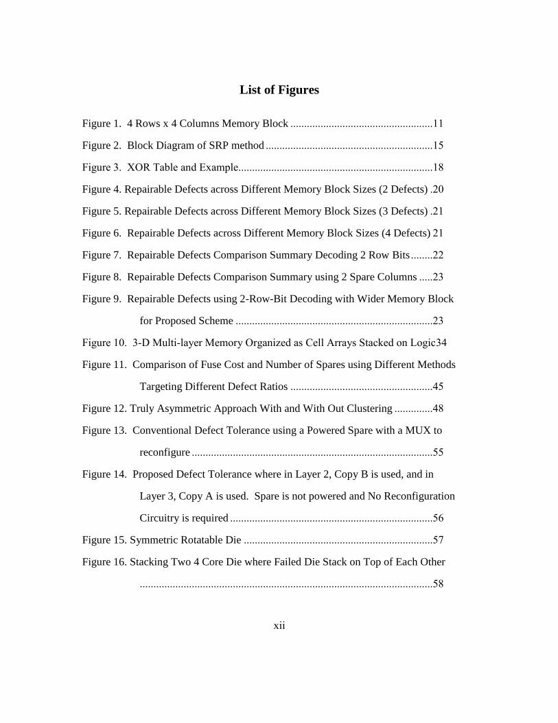
List of Figures ....................................................................................................... xii
Chapter 1: Introduction ...........................................................................................1
1.1. Background ............................................................................................1
1.2. Low Yield ................................................................................................1
1.3. Manufacturing Defects.............................................................................2
1.4. Defect Tolerance ......................................................................................3
1.5. Three Dimensional Integrated Circuits ....................................................4
1.5.1. History..........................................................................................4
1.5.2. Through Silicon Via .....................................................................5
1.5.4. 3-D IC Advantages ......................................................................5
1.5.5. 3-D IC Challenges........................................................................6
1.6. Motivation ................................................................................................7
1.7. Contributions............................................................................................7
1.7.1. Selective Row Partitioning ..........................................................7
1.7.2. Defect tolerance in 3-D IC ...........................................................8
1.7.2.1. Re-ordering dies in stacked memories .............................9
1.7.2.2. Rotational Symmetry in stacked dies ...............................9
1.8. Thesis Organization ...............................................................................10
Chapter 2: Row Partitioning Spare Columns to Improve Yield ...........................11
2.1. The Problem ...........................................................................................11

x
2.2. Related Work .........................................................................................12
2.3. Improving Memory Repair by Selective Row Partitioning ...................13
2.4. Overview of the proposed scheme .........................................................14
2.5. Repair Algorithm ...................................................................................15
2.6. Experimental Results .............................................................................19
2.7. Analysis..................................................................................................24
2.8. Conclusion .............................................................................................26
Chapter 3: Asymmetric Repair in Stacked Memories ..........................................27
3.1. The Problem ...........................................................................................27
3.2. Introduction ............................................................................................27
3.3. Related Work .........................................................................................30
3.4. Overview of the Proposed Scheme ........................................................32
3.5. Procedure for Allocating Spares ............................................................37
3.6. Fine Tuning Domain of Spare................................................................38
3.7. Combining with Selective Row Partitioning .........................................41
3.8. Experimental Setup ................................................................................43
3.9. Results ....................................................................................................45
3.10. Conclusions ..........................................................................................49
Chapter 4: Rotational Symmetry in Stacked Dies .................................................50
4.1. Background ............................................................................................50
4.2. Introduction ............................................................................................52
4.3. Defect Tolerance Based on Layer Ordering ..........................................54
4.4. Defect Tolerance Based on Rotational Symmetry .................................56
4.5. Multiple Rotatable Dies .........................................................................58
4.6. Experimental Results .............................................................................61
4.7. Conclusions ............................................................................................62
Chapter 5: Summary and Future Direction ............................................................64
Bibliography ..........................................................................................................68

xi
List of Tables
Table 1. . Expected distribution of defects/die for 1000 die with 2k bits and bit error
rate of 2-k
. ..........................................................................................34
Table 2. Way to construct 250 4-layer 3-D ICs using the 1000 die shown in Table 1.
...........................................................................................................35
Table 3. Expected distribution of defects/die for 996 die with 2k bits and bit error rate
of 1.5x2-k
. ..........................................................................................36
Table 4. Way to construct 166 6-layer 3-D ICs using the 996 die shown in Table 3.
...........................................................................................................36
Table 5. Domain Selection for Each Spare ............................................................40
Table 6. Tradeoffs for Stacking Arrangement ......................................................61
Table 7. Comparison of Block 1 Implemented with Conventional Defect Tolerance
versus Proposed Defect Tolerance based on Layer Order ................62
Table 8. Comparison of Block 2 Implemented with Conventional Defect Tolerance
versus Proposed Defect Tolerance based on Layer Order ................62
xii
List of Figures
Figure 1. 4 Rows x 4 Columns Memory Block ....................................................11
Figure 2. Block Diagram of SRP method .............................................................15
Figure 3. XOR Table and Example .......................................................................18
Figure 4. Repairable Defects across Different Memory Block Sizes (2 Defects) .20
Figure 5. Repairable Defects across Different Memory Block Sizes (3 Defects) .21
Figure 6. Repairable Defects across Different Memory Block Sizes (4 Defects) 21
Figure 7. Repairable Defects Comparison Summary Decoding 2 Row Bits ........22
Figure 8. Repairable Defects Comparison Summary using 2 Spare Columns .....23
Figure 9. Repairable Defects using 2-Row-Bit Decoding with Wider Memory Block
for Proposed Scheme ........................................................................23
Figure 10. 3-D Multi-layer Memory Organized as Cell Arrays Stacked on Logic34
Figure 11. Comparison of Fuse Cost and Number of Spares using Different Methods
Targeting Different Defect Ratios ....................................................45
Figure 12. Truly Asymmetric Approach With and With Out Clustering ..............48
Figure 13. Conventional Defect Tolerance using a Powered Spare with a MUX to
reconfigure ........................................................................................55
Figure 14. Proposed Defect Tolerance where in Layer 2, Copy B is used, and in
Layer 3, Copy A is used. Spare is not powered and No Reconfiguration
Circuitry is required ..........................................................................56
Figure 15. Symmetric Rotatable Die .....................................................................57
Figure 16. Stacking Two 4 Core Die where Failed Die Stack on Top of Each Other
...........................................................................................................58

xiii
Figure 17. Stacking Two 4 Core Die where Failed Die Do Not Stack on Top of Each
Other .................................................................................................60

1
Chapter 1: Introduction
1.1. BACKGROUND
Integrated Circuit (IC) designs have followed Moore’s law for almost five
decades. Moore’s law states that the transistor density of ICs doubles almost every two
years. This has been possible because of the continuous scaling of the silicon process
technology. As the transistor dimensions shrink, designs benefit in many ways. The
semiconductor industry has been able to produce smaller and faster products due to the
scaling effect. The devices shrink in size allowing more transistors to be packed in a
smaller foot print which in turn reduces overall power consumption. As a result, higher
performing ICs can be built with less cost per function, which leads to greater
profitability. These advantages have accelerated the rate at which the industry adopts
newer technologies.
While Moore’s law has enabled the density of devices to increase, it has also
introduced new challenges, such as low yield. The profitability of IC is also a function of
the fabrication yield, where yield is a ratio of operational devices to the total number of
devices manufactured. Lower yield results in a lot of wasted devices and has a negative
impact on the IC manufacturer’s net profit, which in turn fuels a lot of interest among
researchers to make continuous progress in dealing with yield.
1.2. LOW YIELD
Low yield is an undesirable outcome of the manufacturing process. The
complexity, density and size of the circuit play an important role in determining the yield.

2
As technology scales to smaller dimensions, newer challenges arise. While
nanotechnology based ICs offer advantages such as density and performance, it is
expected to suffer from a significantly increased permanent failure rate. As the transistors
scale to single digit nanometer, higher rates of manufacturing defects are expected.
1.3. MANUFACTURING DEFECTS
Manufacturing defects can be categorized either as global defects or spot defects.
Global defects are larger defects which may be caused by wafer mishandling or
imperfections during etching. These relatively large defects can be controlled by moving
to more sophisticated fabrication lines. Spot defects, which are smaller in size and
random in nature are more difficult to control and hence are a major contributor to yield
loss. Depending on where and when they get introduced and the effect they have, the spot
defects can be further categorized. Photolithographic defects, such as missing or adding
extra metal, diffusion or poly-silicon, are those which get introduced during the
lithographic processes. Moreover, dust particles which contaminate a localized area can
cause defects by either adding or removing material from the vias which are used to
establish contact between the various metal and poly-silicon layers.
Manufacturing defects that have been highlighted thus far, all cause structural
faults. Spot defects which do not cause structural faults will most likely still result in
undesirable operation, such as loss of performance. This can happen if the spot defects
succeed in tampering with the electrical properties of the devices, leading into parametric
faults. One of the major factors in deciding whether or not a defect will manifest as a
structural fault, is the chip density. Dealing with all these manufacturing issues have been

3
a cause of concern and remains a topic of interest among researchers as technology
scaling leads to denser chips. Defect tolerance is one technique to address the
manufacturing defects directly.
1.4. DEFECT TOLERANCE
Transistors with smaller geometry are more susceptible to manufacturing defects.
With the chip density and functionality increasing at a rapid pace, chip designers and
manufacturers continue to be challenged by manufacturing defects in the future.
Furthermore, it is known that the process variations have an amplified effect on devices
as their dimensions shrink resulting in nonoperational, weak and poor performing
devices. While technology scaling satisfies the desire for higher performing, low area
devices, it has made designing for yield enhancement even more economically justifiable.
Conventional defect tolerance involves adding redundant elements and switches
in the design. After manufacture, testing is performed to locate defects, and then
reconfiguration using the switches is performed to bypass the defects so that system
operation is performed using defect-free circuitry [Koren 98].
An important area of design where defect tolerance techniques can significantly
impact overall yield is in memory design. Most of today’s chips are dominated by
memory cells. In fact, SRAM cells are used in caches which take up 50% of the chip area
and constitute 80% of the transistor count [Roelke 07]). The SRAM cell is not only the
most frequently used cell, but also has the smallest geometry transistors, making it the
most susceptible to both device electrical and geometrical variation [Mukhopadhyay 05].

4
Due to these variations, manufacturing reliable memory can become very challenging.
Traditionally defects are tolerated by adding redundancy. Spare rows/columns are added
in the memory and are used to salvage the memories with defects. The spare
rows/columns are put in the design with some additional circuitry to allow the defective
memory location to be swapped with the spare column. The limitation of this approach is
that for memories which have more defective rows/columns than the spare rows/columns
added in the design, the yield loss cannot be prevented.
This thesis addresses how to improve yield and reduce the cost of defect tolerance
in 2D as well as three dimensional integrated circuits.
1.5. THREE DIMENSIONAL INTEGRATED CIRCUITS
1.5.1. History
The insatiable desire for higher computing at the most optimum area, power, price
and performance intersection has pushed the IC industry into a whole new dimension. 3-
D or vertical integration is an exciting new technology which can boost performance and
extend the capabilities of modern ICs. Essentially, it helps with extending Moore’s law
and enables a new generation of tiny but powerful devices. While the opportunities that
3-D ICs offer have been known for a while, it is only recently that the road blocks in the
adaption of this technology have been removed. Some of the early challenges in doing
vertical integration included in-depth knowledge on low temperature bonding and better
understanding of inter layer transfer and alignment. Finally, achievements in the process
of electrical connectivity between layers and progress in an understanding of an effective
release process also helped to push 3-D ICs toward the mainstream.

5
A variety of innovations in the industry have been suggested using 3-D stacking.
System-in-Package (SiP) is one such type of design in which multiple bare dies are
vertically stacked in a single IC package. The different layers are interconnected using
wire-bonds to the substrate. Another example of vertical stacking is the Package-on-
Package (PoP) design, in which multiple packaged chips are vertically stacked. The latest
addition to the list of exciting designs enabled by the emergence of 3-D stacking is the
concept where a single package contains a vertical stack of bare dies interconnected by
means of Through-Silicon Vias (TSVs).
1.5.2. Through Silicon Via
While 3-D ICs can be stacked in multiple ways, TSVs are the most promising
solution as it offers higher density as well as lower capacitance interconnects when
compared to the wire-bond approach. A die can vertically stack on top of another die
using TSVs, which are made of highly conductive material and protrude from the back-
side of a thinned-down die. Among the most compelling benefits which TSVs offer are
shorter interconnect and lesser wire length. The shorter wire length helps with reducing
delays as well as reducing power.
1.5.4. 3-D IC Advantages
3-D IC using TSVs is an important new technology that provides a number of
significant advantages including increased functional density, shorter interconnect, higher
performance, and lower power. Moreover 3-D ICs are attractive not only because they
alleviate interconnect related problems but also facilitate integration of heterogeneous

6
technologies in one single chip [Banerjee 01]. Stacking in a 3-D IC can be done wafer-
to-wafer (W2W), die-to-wafer (D2W), or die-to-die (D2D).
A key advantage that 3-D ICs offer is the drastic decrease in the length of the
longest interconnects across the chip. Another equally important characteristic of 3-D ICs
is the ability to include disparate technologies which offers unique opportunities for
highly heterogeneous and multifunctional systems. Some of the main advantages which
3-D ICs offer are:
1. Shorter interconnects
2. Lower power consumption
3. Increased density
4. Heterogeneous integration
1.5.5. 3-D IC Challenges
While 3-D ICs provide many advantages, there are some challenges as well. 3-D
testing issues and the lack of DFT techniques have made the adoption of this technology
a challenge [Lee 09]. Despite recent advances in design automation tools [Goplen 07],
manufacturing and yield continue to be a point of concern. W2W allows higher
manufacturing throughput, but achieving a good compound yield is difficult. In D2W
and D2D, pre-bond testing can be used to screen out defective die and use only known-
good die (KGD) when constructing the stack. This thesis introduces novel ideas to tackle
the yield challenges of 3-D ICs and does a cost analysis on them.

7
1.6. MOTIVATION
As technology continues to scale to smaller geometries and newer dimensions (3-
D), with increasingly complex manufacturing processes, the ability to reliably
manufacture 100% defect-free circuitry becomes a significant challenge. This work is
motivated by the challenges that yield-enhancing designs face in newer technologies.
While implementing additional circuitry to improve yield is economically
justifiable, this thesis introduces novel techniques to minimize circuitry and improve
efficiency for defect tolerance.
1.7. CONTRIBUTIONS
1.7.1. Selective Row Partitioning
To reduce yield loss due to defects in memory cells, the conventional approach is
to add spare rows and columns to a memory array [Schuster 78], [Zorian 03]. However,
this approach is only useful if the number of defective columns (rows) is less than the
number of spare columns (rows) provided. As the number of defects increase, the ability
to fix only a very limited number of defects is a significant handicap. This thesis
introduces Selective Row Partitioning (SRP), a technique to allow one spare column (or
row) to replace multiple defective columns (or rows). SRP allows a single spare column
to be used to repair multiple defective cells in multiple columns. This is done by
selectively decoding the row address bits when generating the control signals for the
column MUXes. This logically segments the spare column allowing it to replace
different columns in different partitions of the row address space. The hardware is the
same for all chips, but fuses are used to customize the row decoding circuitry on a chip-

8
by-chip basis. An algorithm is described and results presented which show improvement
in overall yield at a minimal overhead cost.
1.7.2. Defect tolerance in 3-D IC
When assembling a 3-D IC, there are several degrees of freedom including which die are
stacked together, in what order, and with what rotational symmetry. This thesis describes
strategies for exploiting these degrees of freedom to reduce the cost and complexity of
implementing defect tolerance. In 3-D memories for example, different architectures exist which
take advantage of TSVs to interconnect multiple layers. One approach is to use stacked banks
where each stacked die contains a different bank of memory. This organization offers significant
reduction in wire-length routing in comparison to a corresponding multi-bank 2D memory.
Cell arrays stacked on logic (using the term from [Taouil 11]) is another exciting new
approach that becomes possible because of TSVs where the upper die layers contain the
cell arrays and the bottom layer implements the peripheral logic (i.e., row decoders,
column select logic, sense amplifiers, row buffers, output drivers, etc.). The advantage of
isolating the peripheral logic on a separate layer is that different process technologies can
be used. For example, cell arrays can be implemented with process technology optimized
for density (e.g., NMOS), whereas the peripheral logic can be implemented with process
technology optimized for speed (e.g., CMOS).
This thesis describes strategies for taking advantage of the new degrees of
freedom which presents itself in 3-D ICs. In particular two new ideas are presented:

9
1.7.2.1. Re-ordering dies in stacked memories
3-D stacking makes it possible to organize memories as cell arrays stacked on
logic where upper die layers contain the cell arrays and the bottom layer implements the
peripheral logic. This allows new degrees of freedom that can be exploited to optimize
the use of spare rows/columns to maximize yield. This thesis exploits the opportunity
presented by the fact that the order of the die in the stack can be selected. The cell array
dies can be ordered such that the most defective cells are at the lowest layer, followed by
next most defective, and so forth, finishing with the die with the fewest defective cells on
the top layer. All the cell array dies have identical designs and are manufactured
identically. However, the peripheral logic die is designed in a way where it costs less to
provide repair on the lower layers than it does on the higher layers of the cell arrays.
This is done by limiting the domain over which some spares can be used thereby
reducing the number of fuses needed for configuring the spare. Experiments show that
the ability to skew repair capability across the different layers in a 3-D IC allows greater
yield enhancement at lower cost both in terms of number of spares and number of fuses.
1.7.2.2. Rotational Symmetry in stacked dies
Conventional defect tolerance schemes involve bypassing defects by
reconfiguring the circuitry so that system operation is performed using defect-free
circuitry. Explicit reconfiguration circuitry is required to perform the reconfiguration,
and the power distribution network must be designed to support all redundant elements.
The schemes proposed in this thesis use the degrees of freedom that exist when a 3-D IC
is assembled at manufacture time to implicitly bypass manufacturing defects without the
need for explicit reconfiguration circuitry. Defects are identified during manufacture test,
and the 3-D ICs are assembled in a way that avoids the use of the defective circuitry. It is
10
shown that leakage power and performance overhead for defect tolerance can be
significantly reduced by exploiting rotational symmetry in stacked 3-D ICs.
1.8. THESIS ORGANIZATION
Chapter 2 discusses one of the main ideas of this thesis. After discussing the
problem and the related work, a detailed overview and algorithm is presented for our
technique. Experimental results and a conclusion are presented in the last two sections of
this chapter.
Chapter 3 explores a new technique for 3-D or stacked memories. It includes a
sub section to show how the idea presented in chapter 2 can be utilized to further improve
the yield in 3-D memories. Experimental results for 3-D memory are show in section
3.10.
Chapter 4 sheds light on other innovative defect tolerance techniques that become
possible because of the degree of freedom which becomes available in the 3-D stacked
ICs. Optimizations and savings in area and yield are studied and presented in this section.
Chapter 5 summarizes the work as well as discusses future direction.

11
Chapter 2: Row Partitioning Spare Columns to Improve Yield
2.1. THE PROBLEM
Fig. 1 shows a block diagram of a traditional 4x4 memory array. The green
blocks indicate the regular memory cells, and the blue boxes indicate the spare column
and spare row added to hide defects. For example, if column0 has one defective cell, it
can be bypassed and the spare column can be used in its place. However, if both columns
0 and 1 have one error each, the memory array becomes unusable and contributes to low
yield. Thus, generally, one spare column (or row) can only replace one column (or row)
containing a defective cell. This is a limitation of current designs.
Figure 1. 4 Rows x 4 Columns Memory Block
12
2.2. RELATED WORK
Traditionally, design time optimizations along with some adaptive design
techniques, and redundancy have been employed to reduce the yield loss due to
manufacturing or parametric shift. These approaches have limitations on the number and
type of failures (read disturb, write failures, access failures) it can repair [Mukhopadhyay
05]. It also has an area, timing and cost overhead. Memory failures are traditionally
compensated for by three main approaches. Firstly, a design time optimization through
selecting the right RAM cell which involves a complex tradeoff between area utilization,
performance, power and yield [Mukhopadhyay 05] may be used. The bigger cell area
usually means more stable memory and better yield but the cell density per area
decreases. Secondly, an adaptive and tunable design which changes the behavior of the
memory cell electrical characteristics based on the process, voltage, and temperature
status on the chip [Mohammad 08] is used. This approach improves yield but cannot fix
all the failures and there will still be some yield loss due to un-tunable cells. The third
approach employed is to repair the failure through swapping the identified failing cells
with working cells. This is done through adding extra memory elements referred to as
redundant columns or rows. Figure 1 shows the basic memory block with main interface
signals and main blocks showing potential redundant cells and fail cells. If there is a
failure in a certain memory bank (identified by BIST) then the entire column/row of the
failing location is swapped out with the spare column/row. This technique works well if
the failures are limited as each additional failure requires a spare column/row. Every bad
cell in a unique memory column requires an additional spare column to rectify it. As we
see in this approach there is a linear dependency of area with the number of fails that can
be tolerated. The addition of these redundant RAM cells and the associated logic (fuses,

13
special BIST) add to the cost of the product [Hamdioui 03]. The approach is also limited
to repair only certain number of cells in a block resulting in yield loss.
Another logical or architectural way of improving yield by making the repair
algorithm more efficient is proposed in [Mohammad 09]. [Mohammad 09] proposes a
solution which dynamically reduces the size of caches, there by taking a performance hit.
It is done by using a state bit which when set indicates that a particular way in the set of
the cache has a defective memory location. The replacement algorithm is then adjusted to
make the set choose between the remainder of the ways only, thereby increasing the miss
rate. This approach can increase the yield at the expense of performance, which may not
be an acceptable trade-off in some of the latest applications.
2.3. IMPROVING MEMORY REPAIR BY SELECTIVE ROW PARTITIONING
The proposed method allows a single spare column to be used to repair multiple
defective cells in multiple columns. This is done by selectively decoding the row address
bits when generating the control signals for the column MUXes. This logically segments
the spare column allowing it to replace different columns in different partitions of the row
address space. The hardware is the same for all chips, but fuses are used to customize the
row decoding circuitry on a chip-by-chip basis. An algorithm is described for choosing
which row address bits to decode given the defect map for a particular chip. This
additional degree of freedom allows customization based on the defect map of a chip and
increases the efficiency of the proposed scheme in comparison to traditional memory
repair. Experimental results show that when compared with traditional schemes of

14
similar complexity, the proposed scheme achieves a higher probability of repairing
defects.
2.4. OVERVIEW OF THE PROPOSED SCHEME
The main motivation behind the proposed scheme is to address the inherent
inefficiency of the conventional approach. Typically an additional spare column is used
in its entirety when repairing a defective cell. This implies that in order to repair multiple
defects, the memory should typically have as many number of spares available as there
are defects in the memory. This is generally true unless a single column in the memory
has more than one defect; in which case the spare, when swapped out with the faulty
column, ends up repairing both of the defects. Such scenarios are rare, thus multiple
spares are added to memories when more defects need to be tolerated. This linear
dependency will lead to excessive overhead as memories continue to be scaled and have
increasingly higher defect rates. The proposed approach increases the efficiency of spare
columns by allowing a single spare column to repair defects in multiple columns by
partially decoding the row address when determining which column is replaced by the
spare. The proposed approach makes use of existing chip repair methodologies. The
novelty in our approach is that given the defect map, it selects n row address bits to
decode so as to allow all defective cells in the memory to be bypassed. Moreover, the
proposed scheme requires the ability to store the information on-chip as to which row
addresses to decode and which column to replace in each partition of the row address
space. This is illustrated in the high level block diagram of the proposed scheme given in
Fig. 2.

15
Figure 2. Block Diagram of SRP method
2.5. REPAIR ALGORITHM
The memory is initially designed with a certain number of spare columns (may be
one, but can be more than one) and the ability to decode a certain number of row address
bits (n). This hardware is fixed for all chips. Given the defect map for a particular chip,
the proposed repair algorithm is used to configure the hardware to bypass the defective
cells. The algorithm first selects the n row address bits to decode based on the defect
map and the number of spare columns available. Decoding the n row address bits
effectively partitions the row address space into 2n different partitions. The spare column
can be used to replace one column in each of the 2n different partitions. So the goal is to
do the partitioning in such a way as to have only a single column in each partition having
a defect. So if there are multiple defects in different columns, the partitioning should be
done such that each partition contains only one defect. This is done by representing each
defect’s row address as a binary number, and then forming a matrix of the XORs of all

16
the pair wise row address combinations. This is illustrated in Figure 3 where the row
addresses of four defects are {000, 010, 100, and 111}. Each of the 6 rows in the table
corresponds to one of the 6 pair wise combinations of the row addresses of the defects,
and each column corresponds to a row address bit. An entry in the matrix is a ‘1’ if the
pair of row addresses of the defects differs in that bit, and a ‘0’ if they are the same.
For example, the row addresses for the defect at “000” and at “010” differ in bit 1,
but not in bits 0 and 2. The goal is to select n row address bits to decode such that each
defect is in a different partition. This corresponds to finding a column cover for the
matrix in which a set of columns is selected such that it contains at least one ‘1’ in each
row. A column cover of this matrix ensures that the selected row address bits will
distinguish every defective row such that no partition will contain more than one defect.
If it is not possible to find a column cover with n or fewer columns, then the memory is
irreparable. Many efficient column covering algorithms exist [Beasley 87].
Once the n row address bits have been selected, the fuses are programmed to
hardcode which row address bits to decode as well as the column that is replaced by the
spare in each partition. This can be done by implementing a small ROM or fuse box. The
ROM drives the select lines of the column muxes which do the actual swapping of the
faulty cell(s) with the good cell(s) from the spare element.
The repair procedure is now illustrated with a small example. Assume that n=2,
so two row address bits are used to partition the spare column in a manner that it can map
each defect in a unique partition of the spare column. The memory used in this example
has 8 rows and 8 columns (C). The row addresses for the defects are {D0, D1, D2, and

17
D3} -> {000, 010, 100, 111}. The XOR between each pair of the row addresses with
defects is performed and stored in a matrix as shown in Fig. 3. A column covering
procedure is then performed which identifies a two bit column cover using bit 2 and bit 1.
Those two row address bits are connected (with fuses) to a ROM (fuse box). The
contents of the ROM are set so that columns 6, 4, 2, 1 are bypassed when the row address
bits are 00, 01, 10, and 11, respectively. The output of the ROM goes to a decoder which
decodes the column to bypass and generates the appropriate set of MUX select signals.
For example, if column 2 is to be bypassed, then the MUX select signals for the
leftmost 3 MUXes are set to select their right input, and the rest of the MUX select
signals select their left input. This uses the spare column and skips column 2. The
additional circuitry required to implement the proposed scheme for the above example is
illustrated in Fig. 3. The fuse box is 2n
(n=2) by log2C (C=8) wide. Additionally a log2C
to C (3 to 8) decoder is needed to generate the C (8) bit MUX select signals.

18
Row Address # Bit 2 Bit 1 Bit 0
(000 ⊕ 010) 0 1 0
(000 ⊕ 100) 1 0 0
(000 ⊕ 111) 1 1 1
(010 ⊕ 100) 1 1 0
(010 ⊕ 111) 1 0 1
(100 ⊕ 111) 0 1 1
Figure 3. XOR Table and Example

19
2.6. EXPERIMENTAL RESULTS
Several simulations were performed to evaluate yield improvements using the
proposed selective row partitioning. For the first set of simulations, two, three and four
random defects were injected across different memory block sizes. We then compared the
traditional probability of repair with a single spare column versus the proposed scheme
using a single spare column and two row address bits for decoding. Fig. 4, 5 & 6 show
the results of these simulations. These simulations were mainly done to see the
effectiveness of the proposed scheme in fixing multiple defects, and also to investigate if
the size of the memory had any impact on the effectiveness of the proposed scheme.
As clearly seen from the results shown in Fig. 4 and Fig. 5, the proposed scheme
is close to 100% effective for two and three defects and there is almost no dependency on
the memory block size. However for four defects, as seen in Fig. 6, the effectiveness of
our approach is clearly dependent on the number of rows. This result is understandable
and expected since the more rows in a block, the more likely it is to find two row bits to
partition the memory with one defect in each partition. Note that for the case of a
traditional single spare, the chance of repairing multiple defects is very low as it depends
on the defects all being in the same column. The probability of this decreases with more
columns or more defects.
Fig. 7 summarizes the comparison between the traditional and proposed scheme
for a 9-row-address-bit and 32-column-bits memory block using one spare column and 2-
address bits for decoding (n=2). As can be seen below the proposed scheme is close to
100% effective for two or three defects, the reason it is not a 100% effective is due to the

20
small chance of defects in the same row. Such defects can obviously not be distinguished
using row address bits for decoding.
For four defects the proposed scheme still achieves close to 80% probability of
repair. This reduction in the probability of repair going from three to four defects is also
expected since partitioning the memory using 2-row-address-bits requires that each of the
four partitions have exactly one defect and there are cases where a solution does not exist.
Figure 4. Repairable Defects across Different Memory Block Sizes (2 Defects)
56
78
9
8
16
32
64
96.70% 98.21% 99.09% 99.68% 99.80%96.84% 98.32% 99.22% 99.69% 99.74%96.75% 98.51% 99.21% 99.61% 99.77%96.90% 98.48% 99.27% 99.59% 99.83%
0.00%
10.00%
20.00%
30.00%
40.00%
50.00%
60.00%
70.00%
80.00%
90.00%
100.00%
% S
olv
ed
No. of Address bits
Num
ber
of
Colu
mns
% Fixable Defects (2 defects) (Proposed Scheme)
8
16
32
64
56
78
9
8
16
32
64
1.53%1.67%
1.64%1.67%
1.48%
3.37%3.15%
3.00%3.25%
3.23%
6.33%6.13%
6.00%5.70%
6.00%
12.56%12.10%
12.30%12.51%
12.12%0.00%
10.00%
20.00%
30.00%
40.00%
50.00%
60.00%
70.00%
80.00%
90.00%
100.00%
% S
olv
ed
No. of Address bits
Num
ber
of
Colu
mns
% Fixable Defects (2 defects) (Traditional)
8
16
32
64

21
Figure 5. Repairable Defects across Different Memory Block Sizes (3 Defects)
Figure 6. Repairable Defects across Different Memory Block Sizes (4 Defects)
56
78
9
8
16
32
64
90.70%95.53% 97.57% 98.81% 99.39%
91.12%95.36% 97.82% 98.87% 99.38%
90.56%95.10% 98.01% 98.68% 99.48%
90.26%95.54% 97.95% 98.71% 99.38%
0.00%
10.00%
20.00%
30.00%
40.00%
50.00%
60.00%
70.00%
80.00%
90.00%
100.00%
% S
olv
ed
No. of Address bits
Num
ber
of
Colu
mns
% Fixable Defects (3 defects) (Proposed Scheme)
8
16
32
64
56
78
9
8
16
32
64
0.02%0.02%
0.02%0.04%
0.04%0.09%
0.06%0.11%
0.12%0.12%
0.37%0.39%
0.31%0.40%
0.40%
1.69%1.84%
1.95%1.57%
1.50%
0.00%
10.00%
20.00%
30.00%
40.00%
50.00%
60.00%
70.00%
80.00%
90.00%
100.00%
% S
olv
ed
No. of Address bits
Num
ber
of
Colu
mns
% Fixable Defects (3 defects) (Traditional)
8
16
32
64
56
78
9
8
16
32
64
47.61%
57.80%
66.74%
75.36%80.23%
47.51%
58.77%
67.35%
74.42%
80.39%
48.77%
58.49%
67.62%
74.98%
80.36%
47.27%
58.37%
67.87%
74.98%
81.15%
0.00%
10.00%
20.00%
30.00%
40.00%
50.00%
60.00%
70.00%
80.00%
90.00%
% S
olv
ed
No. of Row Address bits
Num
ber
of
Colu
mns
% Fixable Defects (4 defects) ( Proposed Scheme )
8
16
32
64
56
78
9
8
16
32
64
0.00%0.00%
0.01%0.00%
0.00%0.00%
0.01%0.01%
0.01%0.01%
0.01%0.00%
0.03%0.05%
0.04%0.10%
0.29%0.12%
0.22%0.17%
0.00%
10.00%
20.00%
30.00%
40.00%
50.00%
60.00%
70.00%
80.00%
90.00%
100.00%
% S
olv
ed
No. of Row Address bits
Nu
mb
er
of
Co
lum
ns
% Fixable Defects (4 defects) (Traditional)
8
16
32
64

22
Figure 7. Repairable Defects Comparison Summary Decoding 2 Row Bits
Fig. 8 shows similar results as Fig. 7 except in this case 2-spare columns are being
used and an attempt is made to solve up to eight defects. This was done to show the
scalability of the proposed scheme. Note that in this case, the same row address bit
decoder is used for both spares. Alternatively, one could use separate row address bit
decoders for each spare, and in that case the effectiveness of each spare would be
equivalent to what was shown in Figure 7.
Memory block (9 row address bits) 32 columns
0.00%
10.00%
20.00%
30.00%
40.00%
50.00%
60.00%
70.00%
80.00%
90.00%
100.00%
0 1 2 3 4
No. of Defects
% S
olve
dProposed Yield
Traditional Yield

23
Figure 8. Repairable Defects Comparison Summary using 2 Spare Columns
Figure 9. Repairable Defects using 2-Row-Bit Decoding with Wider Memory Block for
Proposed Scheme
Comparision of Traditional Vs Proposed
Memory blocks size is 9 row address bits
0.00%
10.00%
20.00%
30.00%
40.00%
50.00%
60.00%
70.00%
80.00%
90.00%
100.00%
0 1 2 3 4
No. of Defects
No. of Column bits for each spare (16 for traditional) and (64 for proposed)
%S
ovle
d
Proposed Yield
Traditional Yield

24
The first set of experiments, summarized in Fig. 7 clearly show the effectiveness
of the proposed scheme in fixing multiple defects, however there is an area overhead cost
associated with implementing the proposed scheme since it requires extra logic (fuses,
muxes, etc.).
An alternative to the proposed approach for improving repair capability would be
to simply use the traditional approach with more spares. To compare these two
alternatives, experiments were performed considering four memory blocks having 9-row-
address-bits and 16-column-bits in which the traditional approach has one spare for each
block. For the proposed scheme we assumed a single memory block with 9-row-address-
bits, 64-column-bits and one spare column. The results are shown in Fig. 9. The
probability of fixing defects with the proposed scheme is clearly better with less spare
columns. The results for the traditional approach can also be probabilistically calculated
and cross checked against the numbers obtained through simulations. In this particular
example, it has been shown that by reducing four spare columns down to one with the
proposed approach, the probability of repairing defects is higher. This advantage comes
from the ability to select which row address bits to decode on a chip-by-chip basis such
that the hardware is effectively customized to the defect map for a particular chip.
2.7. ANALYSIS
In this section simulation results are validated using probability. The equations
can be written in terms of the variables r,k and d. Where r represents total number of row

25
address bits, k represents the number of bits selected for partitioning the spare and d
represents the total number of defects.
The closed form probability can be derived using the formula shown below. The
equations are set up for k = 2. Similar expression could be derived for other values of k.
rd
idr
i
ird
rd
CCd
dkrPdkrP
ddkrP
2
])2()22[(]![
)4,2,1(4,2,2
094.0256
24
2
!)4,2,2(
4
2
2
0
)2(2
1
Using the above expression, the probability when r=3, can then be written as follows:
222.04096
912
4096
)]10()12)[(24(
256
24
2
])2()22[(]!4[
)4,2,2()4,2,3()4)(3(
4
2
423
0
)23(2
1
4
i
i
i CC
dkrPdkrP
And the probability for r = 4, can be written as follows.
356.065536
23328
65536
])10()10)(12()12)[(24(
4096
912
2
])2()22[(]!4[
)4,2,3()4,2,4(
22
)4)(4(
4
2
424
0
)24(2
1
4
i
i
i CC
dkrPdkrP
The formula given above was used to validate the simulation results for the
experiments using the algorithm described in section 2.5. The results correlated very
closely with the calculated probabilities.

26
2.8. CONCLUSION
In this chapter, a scheme is presented for selectively decoding row address bits to
repair multiple defects using a single spare column. This approach is a logical extension
to current approaches where a single spare column replaces another column that has a
defect. The proposed scheme requires some additional logic and fuses to implement,
however it was shown that when comparing the proposed scheme to the traditional
approach of increasing the number of spare to tolerate more defects, for similar
complexity, the proposed scheme achieves a higher probability of repairing defects (Fig.
9). The optimal number of row address bits to decode and memory block size to use
would depend on the process, architecture, and defect rate. Furthermore, this technique
can be employed in conjunction with the existing repair methodology to improve yield in
3-D stacked memories as well.

27
Chapter 3: Asymmetric Repair in Stacked Memories
3.1. THE PROBLEM
In stacked memory arrangement each layer in the stack has identical spare
elements. If a particular layer does not utilize its spare row/column, it can share the
unused redundant row/column with another layer. Repairing a memory location requires
muxing in a defective location with the spare element, which is done by adding additional
circuitry at design time. With a symmetric approach, where spare elements from any
given layer can be used to repair defects in any of the layers, the number of fuses used
may not be optimal. One way this can happen is any time there is a layer which
completely utilizes its spare rows/columns. For such layers it would have been sufficient
to limit the redundancy to the local, smaller space; thereby using fewer fuses. This is one
example of the underlying problem where the number of fuses are not optimized for
yield.
3.2. INTRODUCTION
Stacked memories can be constructed in three-dimensional integrated circuit by
using through silicon vias (TSVs) to interconnect multiple layers. One approach is to use
stacked banks where each stacked die contains a different bank of memory. This
organization offers significant reduction in wire-length routing in comparison to a
corresponding multi-bank 2D memory. Cell arrays stacked on logic (using the term from
[Taouil 11]) is another exciting new approach that becomes possible because of TSVs
where the upper die layers contain the cell arrays and the bottom layer implements the
peripheral logic (i.e., row decoders, column select logic, sense amplifiers, row buffers,
output drivers, etc.). The advantage of isolating the peripheral logic on a separate layer is

28
that different process technologies can be used. For example, cell arrays can be
implemented with process technology optimized for density (e.g., NMOS), whereas the
peripheral logic can be implemented with process technology optimized for speed (e.g.,
CMOS). This approach was first commercially used by Tezzaron Semiconductors. Pre-
bond testing of cell array die has added difficultly, but techniques such as the one
described in [Noia 11] can be used to probe TSVs.
A new idea is proposed in this chapter (preliminary results were presented in [Rab
12]) which exploits an additional degree of freedom which is that the order of the die in a
three-dimensional (3D) memory stack can be selected and optimized. This creates a
degree of freedom which is used to lower the cost of repair and improve yield. This
degree of freedom can be exploited in die-to-wafer (D2W), or die-to-die (D2D) cell
arrays stacked on logic type configurations in the following way. In the proposed
arrangement the lowest die layer will have the dies with the most defective cells,
followed by the next most defective cells in the second lowest layer, and so forth
finishing with the die with the fewest defective cells on the top layer. All the cell array
dies have identical designs and are manufactured identically. The bottom most layer,
which does the peripheral logic, is designed such that it costs less to tolerate defects on
the lower layers than it would on higher layers of the cell arrays. One simple example of
this concept is the following. Suppose there are 4 layers of cell arrays, and each cell
array die contains one spare column, and for simplicity, there are no spare rows. So there
are a total of 4 spare columns. The concept of sharing unused spares among stacked dies
used in [Chi 12] and [Wang 12] could be applied to share the 4 spare columns globally
among all die in the stack which would ensure that any four die with a cumulative total of

29
4 defects or less could be stacked together and be repaired. However, an alternative with
asymmetric layer repair capability would be to dedicate two spares to only be used for the
lowest layer (where the die with the most defects can always be placed) while the other
two spares could be used for any of the four layers. For each spare column that is
dedicated to only be used in one layer (the lowest layer in this example), the space of
possible columns that it can be configured to replace is reduced by a factor of 4 (since
there are 4 layers in this example) meaning that log2(4 layers) =2 less fuses would be
required to implement the reconfiguration logic for each of those spares to select which
column it will replace. Since there are two such dedicated spares in this example, the
total number of fuses for asymmetric repair is reduced by 4 compared to symmetric
repair. In terms of overall repair capability, the asymmetric repair approach could always
handle any stack of four die with a cumulative total of 4 defects or less provided at least
one of those die has 0 defects. So if the overall yield of cell array die with 0 defects is
expected to be greater than 25%, then there will be at least one die with 0 defects that
could be allocated to each stack. Results will be shown later in the chapter that the
overall yield using asymmetric repair can be effectively equivalent to that of symmetric
repair while using fewer fuses, or alternatively for the same number of fuses, the yield
can be improved. Note that each array die is identical, and the proposed method only
impacts the design of the reconfiguration logic on the peripheral layer.
While the simple example above illustrated the concept of asymmetric layer
repair capability using spares dedicated to certain layers, another efficient way that this
concept can be used is with the selective row partitioning (SRP) scheme described in
Chapter 2. SRP provides a way to logically segment a single spare column and use it to

30
repair multiple defective cells in multiple other columns. This capability comes at the
cost of additional fuses, but if it can be utilized to repair multiple defective cells then the
fuse cost per defective cell repaired can be minimized. Using SRP symmetrically for all
layers would tend to be inefficient because some layers may have 1 or 0 defective cells
thereby completely wasting the extra fuses used to implement SRP. However, the
proposed idea here is to use SRP for only one or a few layers and then match up the cell
array die having the most defective cells that can most efficiently benefit with the SRP
layers to efficiently utilize the SRP capability. This would reduce the number of spares
that need to be incorporated in the cell array die thereby reducing the required
redundancy to achieve a given defect tolerance. For example, instead of requiring 2 spare
columns per cell array die, SRP could be used to achieve the same yield using only 1
spare column per cell array die with little or no increase in the number of fuses.
Reducing the cell array size helps reduce area, delay, and power for the overall memory.
3.3. RELATED WORK
Given the high defect rates in memories, spare rows and columns are typically
used to allow for post-manufacturing repair in order to enhance yield [Schuster 78],
[Zorian 03]. The memory is tested, and a defect map is generated indicating which cells
in the memory are defective. Based on the defect map, the memory is reconfigured to use
the spare rows and columns to bypass defective cells [Kuo 87], [Wey 87], [Hemmady
89]. The memory reconfiguration can be done either at manufacture time with fuses, or it
can be done with a built-in self-repair (BISR) scheme [Kim 98].

31
In a conventional single die implementation of a memory, if it is not possible to
repair all the defective cells with the available spare rows and columns, then the die is
discarded as worthless. In a 3D memory where multiple die are stacked together, the idea
of using unused spares in one die to help in repairing another die has been proposed in
[Chou 10, 11] and [Jiang 10]. In these approaches, if there are too many defective cells
to repair using a die’s own intra-die resources, it can borrow unused spares from other
die. This is applicable for any of the integration methods, i.e., wafer-to-wafer (W2W),
die-to-wafer (D2W), or die-to-die (D2D). However, it is especially powerful for D2W
and D2D where the specific die to be stacked together can be selected to optimize overall
yield. For example, consider the case where each die contains one spare row and one
spare column. With the ability to share spares across die, then dies with 4 defects could
be stacked together with dies containing 0 defects, and dies with 3 defects could be
stacked with dies containing 1 defect, and so forth. So by categorizing every die in a lot
and carefully distributing them among the various 3D stacks, the number of unusable die
can be minimized. The schemes in [Chou 11] and [Jiang 10] were conceived for a
stacked banks type configuration for 3D memory using additional TSVs to share spares
across layers, but the same concept could be applied for a cell arrays stacked on logic
type configuration also where the row decoders, column select logic, and reconfiguration
logic is all located on the bottom layer.
In [Chi 12], a more general method for sharing spares across layers was presented
for processor-memory stacks in which a stacked banks type of configuration is used for
the memory, but on the processor die, a global spare assignment unit is placed which can
allocate spares across the layers. [Wang 12] uses a similar approach, and also proposes

32
the use of a spare cylinder which replaces all the cells in a vertical axis across multiple
die.
The asymmetric layer repair method proposed in this chapter is for the cell arrays
stacked on logic memory architecture and takes advantage of the degree of freedom that
the order of the die in the stack can be chosen. It differs from earlier methods in that it
optimizes repair configuration logic by exploiting the fact that dies with more defects can
be placed in certain layers in the stack which allows greater yield enhancement at lower
cost both in terms of number of spares and number of fuses.
3.4. OVERVIEW OF THE PROPOSED SCHEME
Figure 10 shows a block diagram of a 3-D multi-layer memory organized as cell
arrays stacked on logic. All the cell array dies are identical. The spare columns and rows
are evenly distributed among the layers. The row decoder, column select logic, and other
peripheral logic are located in a separate logic layer. The fuses for configuring the spares
to perform repair are also located on the logic layer. To maximize the repair capability,
the spares could be used for global inter-die repair. In other words, each spare column
(row) could be used to replace any column (row) on any layer. The main cost for this
would be the number of fuses needed to configure each column (row) globally across all
layers. If there are n layers and c columns (r rows), the number of fuses needed to make
each spare column (row) a global spare that can be used to replace any bit line (word
line) in any layer would be log2[n] to select the layer and log
2[c] (log
2[r]) to select the bit
line (word line). So the cost of a global spare versus the cost of a spare local to one die is
the following:

33
Fuses for global spare = log2[c] (or log
2[r]) + log
2[n]
Fuses for local spare = log2[c] or log
2[r]
The proposed idea is to consider allowing some spares to be global and some to
be local rather than the conventional symmetric design having all local spares or all
global spares. The optimal number of local and global spares and their distribution
across the layers depends on the expected distribution of defects. Without loss of
generality, consider the case where defects are equally likely in each cell of each die (i.e.,
they are not clustered in certain die). Suppose 1000 die are manufactured each
containing 2k bits and the bit error rate is 2
-k. Then the expected distribution of
defects/die is shown in Table 1. If there are 4 layers and 4 global spares, then the 1000
die can be combined together to construct 250 3-D ICs with the configuration shown in
Table 2. As can be seen from Table 2, 15 3-D ICs would combine one die with 4 defects
together with three die having 0 defects. 61 3-D ICs would combine one die with 3
defects, one die with 1 defect, and two die with 0 defects, and so forth.
Using the proposed approach, we can exploit the degree of freedom of which
order the die are stacked. The peripheral logic built on the logic array can be designed so
that it always allocates two local spares to the lowest layer and then two global spares
that can be used in any layer. The die with the most defects is then always placed in the
lowest layer. As can be seen in Table 2, all the configurations that are used have at least
one die with 2 defects. Thus, the two local spares are fully utilized. Since all
configurations have no more than 4 defects in total, the combination of the 2 fully utilized
local spares plus the 2 global spares can repair all the defects in all the configurations.
Thus the yield in this case would be identical to using 4 global spares, but the advantage

34
is that the number of fuses is reduced by 4 because each local spare needs log2(4 layers)
fewer fuses.
Figure 10. 3-D Multi-layer Memory Organized as Cell Arrays Stacked on Logic
Table 1. . Expected distribution of defects/die for 1000 die with 2k bits and bit error rate
of 2-k
.
Defects/Die Number of
Die
0 370
1 370
2 184
3 61
4 15
spare row
spare
column
spare row
spare
column
spare row
spare
column
spare row
spare
column
spare row
spare
column
Cell Array Layer
Logic Layer
Column Select
Row
Decoder
Fuses

35
Table 2. Way to construct 250 4-layer 3-D ICs using the 1000 die shown in Table 1.
Num. Config. Defects/Die
3-D ICs 4 3 2 1 0
15 4-0-0-0 15 0 0 0 45
61 3-1-0-0 0 61 0 61 122
10 2-2-0-0 0 0 20 0 20
145 2-1-1-0 0 0 145 290 145
19 2-1-0-0 0 0 19 19 38
250 Total 15 61 184 370 370
Now consider a second example where 996 die are manufactured each containing
2k bits and the bit error rate is 1.5x2
-k. The expected distribution of defects/die is shown
in Table 3. If there are 6 layers and 2 global spares per die, then 166 3-D ICs can be
constructed using the configurations shown in Table 4.
Using the proposed method, 3 local spares could be allocated for the lowest layer,
2 local spares could be allocated for the second lowest layer, 1 local spare could be
allowed for the third lowest layer, and 3 global spares could be used to cover the rest of
the defects not covered by the local spares. Thus a total of 9 spares is required with 6 of
those being local and only 3 of them being global. This helps to significantly reduce the
number of fuses required.

36
A procedure for allocating local and global spares to minimize the number of
spares and number of fuses is given in the next section.
Table 3. Expected distribution of defects/die for 996 die with 2k bits and bit error rate of
1.5x2-k
.
Defects/Die Number of
Die
0 222
1 334
2 251
3 125
4 47
5 14
6 3
Table 4. Way to construct 166 6-layer 3-D ICs using the 996 die shown in Table 3.
Num. Config. Defect/Die
3D-ICs 6 5 4 3 2 1 0
3 6-2-1-0-0-0 3 0 0 0 3 3 9
14 5-2-1-1-0-0 0 14 0 0 14 28 28
47 4-2-2-1-0-0 0 0 47 0 94 47 94
23 3-3-1-1-1-0 0 0 0 46 0 69 23
61 3-2-2-1-1-0 0 0 0 61 122 122 61
11 3-2-1-1-1-1 0 0 0 11 11 44 0
7 3-2-1-1-1-0 0 0 0 7 7 21 7
166 Total 3 14 47 125 251 305 215

37
3.5. PROCEDURE FOR ALLOCATING SPARES
Given an expected defect distribution (i.e., the information shown in Tables 1 and
3), the following procedure can be used to configure the die in the layers to construct 3-D
ICs to minimize the total number of spares required and maximize the number of local
spares (i.e., to obtain the information shown in Tables 2 and 4).
Step 1: Set the total-defect-limit per 3-D IC equal to the number of defects in the
die with the most defects.
Step 2: Fill the lowest layer of each of the n 3-D ICs with the n die having the
most defects.
Step 3: For the next lowest layer, fill each of the n 3-D ICs from the population
of remaining die placing the most defective die in the 3-D IC with the fewest total
defects under the constraint that the total defects in any 3-D IC does not exceed
the total-defect-limit.
Step 4: Step 3 is repeated until all layers are filled at which point the procedure
completes. However, if a point is reached where it is impossible to fill a 3-D IC
from the population of remaining die without violating the total-defect-limit
constraint, then the total-defect-limit is incremented by 1 and the procedure starts
over from Step 2.
Once the procedure above is completed, then the set of possible distributions of
defects per layer is known. The final total-defect-limit is the total number of spares
required. The minimum number of defects in a particular layer is the number of local
spares that can be fully used for that layer. If some distributions have 0 defects in some

38
layer, then no local spares can be fully used for that layer. Once the local spares are
determined, then the number of global spares is simply the total number of spares minus
the number of local spares.
The above procedure gives the minimum total number of spares. However, in
some cases some global spares can be converted to local spares (i.e., with no net increase
in the total number of spares) while still satisfying the constraints. This arises because
the number of spares has to be a whole number, so there can be some slack. So a final
post-processing step would be to iterate through each layer and try to convert a global
spare to become a local spare for that layer while still satisfying the constraints.
This design procedure described in this section uses enough spares to ensure that
all die in the considered distribution can be repaired and utilized (i.e., 100% utilization).
If it is acceptable to allow some of the die with the most defects to be discarded (i.e.,
have less than 100% utilization), then the same procedure can still be used. The input
distribution would simply be adjusted based on the desired utilization. For example, if it
is acceptable to discard all die with 4 or more defects, then the input distribution for the
procedure would only contain the population of die with fewer than 4 defects. Under this
condition the procedure would minimize the number of total spares and maximize the
number of local spares.
3.6. FINE TUNING DOMAIN OF SPARE
When memories are arranged as cell arrays stacked on logic it allows for a degree
of freedom which can be exploited to optimize the use of spare rows/columns to

39
maximize yield. In Sec. 3.4, it was shown how this degree of freedom can reduce the
cost, in terms of fuses, of yield enhancement. So far in the chapter a local spare has been
defined as one which is restricted to a particular layer in the stacked IC. Similarly a
global spare is defined to be one which is capable of tolerating a defect in all the layers of
the stack. While this approach is successful in reducing the overall cost of repairing
defects, it does not completely exploit the degree of freedom offered by this memory
architecture. In this section, the domain selection process is generalized to achieve greater
reductions.
By allowing spares to cover a smaller domain than a single layer, the cost of
repair can be lowered further. For example a local spare can be restricted to a subset of
the columns in that particular layer, thereby lowering the repair cost since fewer fuses are
needed to implement it. Similarly a global spare can also be restricted to any subset of
layers as opposed to all the layers. By fine tuning the local spares to a smaller set within
the layer and the global spares to a subset of the layers, the number of fuses required
reduces even more as compared to the approach discussed in Sec. 3.4 where spares are
restricted to only global or local to one layer.
To illustrate this concept, consider the example from Sec. 3.4 of a 4 layer stack
with a defect ratio of 1.0 and a total of 1000 dies. It has 250 stacks of 4 dies in each stack
with the distribution shown in Table 1.
By using the algorithm described in Sec. 3.5, it is known that the total number of
spares needed to tolerate all the defects in each of the stack is four (maximum of the sum
of the defects in each stack). After going through the complete algorithm it is shown (in

40
Sec. 3.4) that the peripheral logic built on the logic array can be designed so that it
always allocates two local spares to the lowest layer and then two global spares that can
be used in any layer as seen in Table 2. This saves a total of four fuses.
By further fine tuning the domain for local and the global spares, as described
earlier in this section, we can reduce 1 more fuse. Since we have a layer (top layer) with 0
defects, none of the spares would need to tolerate a defect in that layer. Similarly in the
next layer the most defective die has one defect; hence covering that layer with only of
the two global spares should be sufficient. Below we show how we can assign the global
and local spares
Table 5. Domain Selection for Each Spare
Num. Config. Local and Global Domain
3-D ICs {L0-1-2-3} Local Local G0 G1
15 4-0-0-0 1 1 L0 L0
61 3-1-0-0 1 1 L0 L1
10 2-2-0-0 1 1 L1 L1
145 2-1-1-0 1 1 L1 L2
19 2-1-0-0 1 1 L1 -
One of the global spares (G0 in Table 5) only has to repair a defect in either layer
0 (L0 in Table 5) or layer 1 (L1 in Table 5). Therefore by fine tuning the domain over
which each of the global spares are capable to repair defects, the number of fuses is
41
reduced by 1 because one of the global spare needs log2(2 layers) fewer fuses. This
increases the savings from 4 fuses to 5.
In the results section, experimental results for fine tuning the domain of each
spare is shown where the cost, in terms of fuses, of yield enhancement is reduced over
several defect ratios and stacked ICs.
3.7. COMBINING WITH SELECTIVE ROW PARTITIONING
Another very efficient way that the proposed concept can be used is with the SRP
scheme described in Chapter 2. The SRP method selectively chooses one or more row
address bits to decode thereby partitioning the row address space. The column that is
replaced by a particular spare column can be different for each partition of the row
address space. This allows a single spare column to repair multiple defects provided each
defect exists in a different partition of the row address space. The cost of SRP is that the
number of fuses required for configuring the spare column is now multiplied by the
number of row address partitions since it can be different in each row addresses partition.
For example, suppose the number of columns is c. If SRP was used to decode two row
address bits and create 4 partitions of the row address space, then the number of fuses
required would be 4 log2(c). However, if 4 defects are repaired, then the fuse cost is the
same as if four separate spare columns were used to repair the four defects each requiring
log2(c) fuses. On the other hand, if only 3 defects are repaired, then the number of fuses
is higher for SRP with one spare column compared to using 3 spare columns (i.e., 4
log2(c) vs. 3 log2(c)). So the efficiency of SRP depends on how much of the maximum
repair capability of SRP can be utilized.

42
With the proposed idea of asymmetric repair, it is possible to use SRP for one
layer and then select a die whose defect profile can be most efficiently repaired with SRP.
By selective matching up die with layers implementing SRP, the repair capability of the
SRP can be efficiently used. When it is possible to always maximally use the SRP repair
capability, then there is no additional fuse cost for using SRP. Thus it can effectively
either reduce the total number of spares required for a given yield or enhance the yield for
a given number of spares without requiring additional fuses. If SRP’s repair capability
cannot always be maximally used, then there is some fuse overhead for using SRP
compared with using more spares, but it still may be worthwhile. For example, it may be
possible to reduce the number of spares included in each cell array die by using SRP at
the cost of more fuses. So the tradeoff would be the cost of the additional fuses versus
the area, delay, and power reduction resulting from reducing the number of spares on
each cell array die.
SRP can be used by first selecting spares using the procedure in Sec. 3.5. A
subset of the local spares in some layer can be replaced by SRP. The smaller the number
of partitions that are used by SRP, the higher the utilization of repair capability will be.
In the results section, results are shown for two cases. One is where SRP is used only
when it will not increase the number of fuses (i.e., its capacity is fully utilized), and the
other is where SRP is used more aggressively so that the number of spares per cell array
die is reduced at some cost in terms of additional fuses.

43
3.8. EXPERIMENTAL SETUP
Simulations were performed targeting different defect ratios where the defect ratio
is defined as the average number of defective memory cells per cell array die. Note that
the proposed method does not require knowing the exact defect ratio that will exist when
the cell array die are manufactured, it simply targets some maximum defect ratio for
which it is desired that the repair capability be able to handle.
The results are shown in Fig. 11 assuming a uniform distribution of defects across
memory cells and die. Results are plotted for five different methods providing repair
capability sufficient for the targeted defect ratio. The first is the conventional symmetric
repair where all spares were considered to be global. The second is the proposed
asymmetric repair (Sec. 3.4) where the procedure in Sec. 3.5 is used to select local and
global spares. The logic layer is designed to implement these spares using the minimum
number of fuses. The third method is using the proposed asymmetric repair with SRP
only when it does not increase the number of fuses. The fourth method is using the
proposed asymmetric repair with aggressive use of SRP sufficient to reduce the number
of spares required per cell array die. The fifth approach is using the technique described
in section 3.6 to improve domain selection for each of the spares. The results were
generated assuming 3 layers, 4 layers, and 6 layers of cell array dies. For each number of
layers, there is one graph for the number of fuses per targeted defect ratio and another
graph for the total number of spares per targeted defect ratio. Note that the total number
of spares is a multiple of the number of layers since each cell array die is identical and
contains the same number of spares. Furthermore only four approaches are shown in the
spares results since both the asymmetric approaches (Sec. 3.4 and Sec. 3.6) use identical

44
number of spares. The savings is only in the number of fuses if truly asymmetric
approach is used.
From the results, it can be seen that the number of fuses can be significantly
reduced using the proposed asymmetric repair approaches. If SRP is used, in some cases
the number of spares per cell array die can also be reduced without any increase in the
number of fuses (e.g., when the defect ratio is 2.25 or 2.5, one spare per die can be
reduced with no increase in the number of fuses). Finally, if SRP is used more
aggressively, it is possible to reduce the number of spares per cell array die at the cost of
more fuses. Note that the total number of fuses required to reduce the number of
spares/die is generally less than the number of fuses required for conventional symmetric
SRP.
The results in Fig. 11 are conservative in that they assume defects are uniformly
distributed which is the worst case for the proposed method. To see how clustering of
defects would impact the results, experiments were performed where defects were
modeled using the Polya Eggenberger distribution with =2.130 and =2.382 [Strapper
80] to represent the case with clustered defects. In Fig. 12, the cost of fuses with a
distribution with clustering is compared against the results with a uniform distribution for
the fine-tuned asymmetric case. As can be seen, the results are somewhat better when
there is clustering.
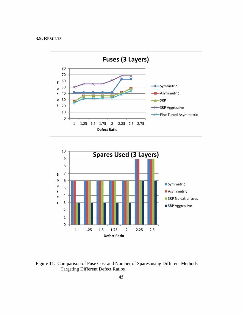
45
3.9. RESULTS
Figure 11. Comparison of Fuse Cost and Number of Spares using Different Methods
Targeting Different Defect Ratios
0
10
20
30
40
50
60
70
80
1 1.25 1.5 1.75 2 2.25 2.5 2.75
F
u
s
e
s
Defect Ratio
Fuses (3 Layers)
Symmetric
Asymmetric
SRP
SRP Aggressive
Fine Tuned Asymmetric
0
1
2
3
4
5
6
7
8
9
10
1 1.25 1.5 1.75 2 2.25 2.5
S
p
a
r
e
s
Defect Ratio
Spares Used (3 Layers)
Symmetric
Asymmetric
SRP No extra fuses
SRP Aggressive

46
Figure 11. Comparison of Fuse Cost and Number of Spares using Different Methods
Targeting Different Defect Ratios
0
10
20
30
40
50
60
70
80
90
1 1.25 1.5 1.75 2 2.25 2.5
F
u
s
e
s
Defect Ratio
Fuses (4 Layers)
Symmetric
Asymmetric
SRP
SRP Aggressive
Fine Tuned Asymmetric
0
2
4
6
8
10
12
14
1 1.25 1.5 1.75 2 2.25 2.5
S
p
a
r
e
s
Defect Ratio
Spares Used (4 Layers)
Symmetric
Asymmetric
SRP No extra fuses
SRP Aggressive

47
Figure 11. Comparison of Fuse Cost and Number of Spares using Different Methods
Targeting Different Defect Ratios
0
20
40
60
80
100
120
140
160
1 1.25 1.5 1.75 2 2.25 2.5
F
u
s
e
s
Defect Ratio
Fuses (6 Layers)
Symmetric
Asymmetric
SRP
SRP Aggressive
Fine Tuned Asymmetric
0
2
4
6
8
10
12
14
16
18
20
1 1.25 1.5 1.75 2 2.25 2.5
S
p
a
r
e
s
Defect Ratio
Spares Used (6 Layers)
Symmetric
Asymmetric
SRP No extra fuses
SRP Aggressive

48
Figure 12. Truly Asymmetric Approach With and With Out Clustering
20
25
30
35
40
45
50
1 1.25 1.5 1.75 2 2.25 2.5 2.75
F
u
s
e
s
Defect Ratio
Clustering on True Asymmetric (3 Layers)
Uniform
Clustering
25
30
35
40
45
50
55
1 1.25 1.5 1.75 2 2.25 2.5
F
u
s
e
s
Defect Ratio
Clustering on True Asymmetric (4 Layers)
Uniform
Clustering
25
35
45
55
65
75
85
1 1.25 1.5 1.75 2 2.25 2.5
F
u
s
e
s
Defect Ratio
Clustering on True Asymmetric (6 Layers)
Uniform
Clustering
49
3.10. CONCLUSIONS
The new concept of asymmetric repair described in this is made possible by the
degree of freedom in multi-layer 3-D IC memories that the order of the die in the stack
can be selected. By matching up die with more defects to layers that have greater repair
capability, the number of fuses required to handle a particular defect ratio is significantly
reduced. Moreover, the SRP technique from chapter 2 can be efficiently utilized to also
reduce the number of spares per cell array. It is also shown that by fine tuning the domain
of each spare further cost reduction in fuses is possible. Finally, the results show that the
proposed scheme works best when faults are clustered together. This is because
clustering increases the number of zero-fault dies and also increases the number of multi-
fault dies. The increase in multi-fault dies increases the assignment of local spares,
whereas the increase in the number of zero-fault dies help with the better selection of
global spares.
In this chapter it was shown how defect tolerance can be made more efficient in a
3D memory design. However by exploiting degrees of freedom which exists when
assembling a 3-D IC, the cost of defect tolerance can be reduced in other, non-memory,
types of 3-D ICs as well. In the next chapter a technique to lower defect tolerance cost for
3-D ICs will be presented.

50
Chapter 4: Rotational Symmetry in Stacked Dies
4.1. BACKGROUND
As technology aggressively scales, 3D stacking of devices have become a viable
solution for building high performing ICs. Stacking in a 3-D IC can be done wafer-to-
wafer (W2W), die-to-wafer (D2W), or die-to-die (D2D). Other stacking methods such as
die-partial wafer bonding, partial wafer-partial wafer bonding are also briefly discussed
in [Black 06]. The most commonly used are W2W or D2D bonding, and each have their
own advantages [Patti 06]. W2W has a better manufacturing throughput while it may
suffer from lower yield. Techniques to overcome the yield challenges in W2W stacking
are introduced in several of the recent work such as that in [Reda 10]. The D2D stacking
on the other hand has the advantage of doing known-good-die testing after manufacture
which helps with improving yield.
W2W stacking and alignment can be done in various ways as presented and
compared in [Lindner 02]. [Lindner 02] explains the steps involved in the stacking
procedure which includes the application of the intermediate layer, wafer alignment and
bonding. The main idea, as the name suggests, involves vertically stacking the wafers
using one of several bonding methods [Morrow 04 and Lindner 02]. The most commonly
used is through TSVs.
D2D stacking has two natural topologies, face to face and face to back, where a
die’s face is the side with the metallization and its back is the side with the silicon
substrate [Loh 07]. [Loh 07] explains how the copper deposits are done on each layer to
form the bonding between the two dies. Similar to the W2W stacking, D2D stacking also
involves the use of TSVs to build the connection through the layers of the die stacks.

51
TSVs are the most common solution for stacking as it offers higher density as
well as lower capacitance interconnects when compared to the wire-bond approach. A die
can vertically stack on top of another die using TSVs, which are made of highly
conductive material and protrude from the back-side of a thinned-down die. Among the
most compelling benefits which TSVs offer are shorter interconnect and lesser wire
length. The shorter wire length helps with reducing delays as well as reducing power.
Vias can be introduced during various stages of the stacking flow. These are
classified as via-first, via-middle or via-last. Depending on the final product, the choice
of via-first or via-last can be made [Knickerbocker 08 and Henry 07]. [Laviron 09]
explains the difference between the via-first and via-last approaches. The via-first
approach is when the TSVs are formed on the device side of the wafer before the bonding
process. [Laviron 09] also discusses what material to use and when to introduce the TSV
bricks depending on thermal budget limitation. One advantage of the via-first approach is
that the TSV brick does not impact the post process flow as the via is fully filled and
planarised. In the TSV last process the fabricated wafers are bonded and then the
substrate is thinned before forming the TSV [Burns 06].
In this chapter novel techniques to do implicit defect tolerance will be introduced.
The techniques that will be discussed are for D2D stacking. The ideas require that the
dies have all been manufactured identically, then after testing and locating the defective
portions or modules of the design, stacking arrangement can be done to do implicit defect
tolerance. The techniques will work equally with either TSV-first or TSV-last methods.

52
4.2. INTRODUCTION
When assembling a 3-D IC, there are several degrees of freedom including which
die are stacked together, in what order, and with what rotational symmetry. This chapter
describes strategies for exploiting these degrees of freedom to reduce the cost and
complexity of implementing defect tolerance. Conventional defect tolerance schemes
involve bypassing defects by reconfiguring the circuitry so that system operation is
performed using defect-free circuitry. Explicit reconfiguration circuitry is required to
perform the reconfiguration, and the power distribution network must be designed to
support all redundant elements. The schemes proposed in this chapter use the degrees of
freedom that exist when a 3-D IC is assembled at manufacture time to implicitly bypass
manufacturing defects without the need for explicit reconfiguration circuitry. Defects are
identified during manufacture test, and the 3-D ICs are assembled in a way that avoids
the use of the defective circuitry. It is shown that leakage power and performance
overhead for defect tolerance can be significantly reduced.
3-D ICs using through-silicon vias (TSVs) is an important new technology that
provides a number of significant advantages including increased functional density,
shorter interconnect, higher performance, and lower power. Stacking in a 3-D IC can be
done wafer-to-wafer (W2W), die-to-wafer (D2W), or die-to-die (D2D), as mentioned in
chapter 3. W2W allows higher manufacturing throughput, but achieving a good
compound yield is difficult. In D2W and D2D, pre-bond testing can be used to screen
out defective die and use only known-good die (KGD) when constructing the stack.
As technology continues to scale to smaller dimensions, with increasingly
complex manufacturing processes, the ability to reliably manufacture 100% defect-free

53
circuitry becomes a significant challenge. It is widely recognized that future technologies
will need to rely on defect tolerance techniques. The cost benefits of using defect
tolerance techniques to boost yield are becoming increasingly compelling. Conventional
defect tolerance involves adding redundant elements and switches in the design. After
manufacture, testing is performed to locate defects, and then reconfiguration using the
switches is performed to bypass the defects so that system operation is performed using
defect-free circuitry [Koren 98].
The idea proposed here is to implement defect tolerance by using these degrees of
freedom to implicitly bypass defects without the need for explicit reconfiguration
circuitry. For D2D stacking, the dies that are used to assemble the 3-D IC are
manufactured and tested resulting in a repository of dies in which the location of the
defects is known. From this repository, the goal is to assemble the maximum number of
3-D ICs (i.e., maximize yield) in which the defects are bypassed so that defect-free
system operation can be performed. The key idea is to make the design such that the
computing elements that are used differ depending on which layer or which rotational
symmetry is used. So a die with a defect in a certain location may be usable in certain
layers or certain rotational symmetries, but may not be usable in others. Since the
repository contains a large selection of die with different defects, the dies can be matched
together in an optimal way when assembling the 3-D ICs so as to maximize the overall
yield of 3-D ICs. The advantages of this approach include eliminating the need for
switches and explicit reconfiguration circuitry and its associate overhead. Another
advantage is the power distribution network in the surrounding layers need only be
designed to support the computing elements being used and not the redundant elements.

54
This is a big advantage as it avoids leakage current in the redundant elements and allows
for a less expensive power/ground distribution network to be used.
While the proposed defect tolerance techniques can be used for memories, they
are more suited for logic elements. Because memories have a very regular structure, very
efficient defect tolerance techniques based on using spare rows and columns are already
available [Schuster 78], [Zorian 03]. Recent work in [Chou 09, 10, 11], and [Jiang 10]
has proposed techniques for using unused spares in one die to help in repairing another
die in an adjacent layer in 3-D ICs. This approach allows memory die to be matched up in
a way that maximizes yield when assembling 3-D ICs. Chapter 3 also introduced a novel
technique for optimizing the number of spares used in a 3D memory design.
Earlier work in defect tolerance for logic circuits has investigated using arrays of
regular processing arrays including linear arrays, rectangular arrays, and binary tree
architectures in which spares are included [Singh 88]. The schemes described in this
chapter can be applied for these types of architectures where the processing elements are
distributed across multiple die. This can be done in a way that avoids the need for
explicit reconfiguration circuitry.
4.3. DEFECT TOLERANCE BASED ON LAYER ORDERING
Consider a 3-D IC where the two middle layers contain identical die, as shown in
Fig 13. The two middle die can be designed with one or more sub-modules duplicated.
The other layers can be designed so that it always interfaces to and uses copy A of all
duplicated sub-modules in the 3rd layer die, and always uses copy B of all duplicated

55
sub-modules in the 2nd layer die. If a die has a defect in copy A of some duplicated sub-
module, that die could be stacked so that it is in the 2nd layer where copy B is used. If a
die has a defect in copy B of some duplicated sub-module, that die could be stacked so
that it is in the 3rd layer where copy A is used.
After manufacture, the dies are tested and the defects located. The repository of
die would include some die that are defect-free, some that have a defect in copy A, and
some that have a defect in copy B. When assembling the 3-D ICs, the dies with defects
would be placed in the appropriate layer where the defect is bypassed. The defect-free
dies could be place in either layer. In this manner, the overall yield of operational 3-D
ICs that can be constructed from the die can be maximized. Yield would only be lost for
die which had defects in both copy A and copy B.
Experimental results highlight the reduction in area and power by taking
advantage of the layer ordering for redundant logic. Results are shown in section 4.6.
Layer 3
Copy A Copy B
Mux
Layer 2
Copy A Copy B
Mux
Figure 13. Conventional Defect Tolerance using a Powered Spare with a MUX to
reconfigure

56
Layer 3
Copy A Copy B
Layer 2
Copy A Copy B
Figure 14. Proposed Defect Tolerance where in Layer 2, Copy B is used, and in Layer 3,
Copy A is used. Spare is not powered and No Reconfiguration Circuitry is
required
4.4. DEFECT TOLERANCE BASED ON ROTATIONAL SYMMETRY
The idea of using rotational symmetry was proposed in [Singh 11] at the wafer
level for W2W stacking in 3-D ICs. The idea is to place die symmetrically on the wafer
so that the wafer can be rotated 90 degrees at a time yielding 4 different rotational
symmetries. This increases the number of ways that wafers can be matched together in
W2W stacking. In this chapter, we propose to use rotational symmetry for D2D stacking
as illustrated in Fig. 15.
Rotational symmetry can be used as an effective defect tolerance strategy in
designs which have spares in a die. Consider a 3-D IC where one layer contains a die
with four identical cores. Three functional cores are needed, and one is a spare. If the
die can be layed out symmetrically as shown in Fig. 15, then it is possible to rotate the die
to always place the defective core in say, the southwest quadrant when bonding the die to
the 3-D IC stack. The other layers can be designed knowing the core in the southwest
quadrant will not be used. This eliminates the need for any explicit reconfiguration
mechanism and avoids the associated power and performance overhead. Moreover, no

57
TSVs, power distribution network, or DFT support would need to be designed on the
other layers (surrounding the symmetric die) to support the core in the unused quadrant.
This avoids power dissipation, including static power dissipation, in the unused core and
reduces both functional as well as power/ground TSVs running to the unused core. This
helps improve manufacturability and yield because there are fewer things that can fail,
while still providing the desired defect tolerance coming from having a spare core.
Figure 15. Symmetric Rotatable Die
A couple of issues for implementing this approach include the following. First,
the die needs to be square in order to have this symmetry. Second, buses and signals that
are passing through this layer to interface with other layers would need to be designed so
that they have a symmetric layout so that rotating the die will not affect them (i.e., there
will still be a TSV/wire connecting them regardless of the rotation).
Note that the example in Fig. 15 shows 4 cores. It is also possible to implement a
symmetric rotatable die using 2 cores with one on each half of the die. In this case, the
die does not have to be square as the rotation would be 180 degrees.

58
4.5. MULTIPLE ROTATABLE DIES
Current and future multi-core CPUs achieve high core counts by increasing the
size of the processor die. As die size and transistor density grow, the susceptibility of
these processors to hard faults grows as well [Powell 09]. Furthermore, ongoing research
suggests that next generation designs should be optimized for performance, area and
thermal issues jointly [Li, 06]. The longevity and the reliability of the cores are a function
of the heat dissipation within the core. Hot spot formations and other undesirable
conditions may occur due to variations in heat dissipation within the core. Hot spots can
be formed, for example, when a high power core gets integrated with low power
memories, thereby creating localized high power regions. It is expected that the heat flux
emanating from hot spots in the next generation microprocessors may exceed 100W/cm2,
six times more than the average heat flux on the die [Yang 07]. Rotational symmetry can
be applied in multi-layered, multi-core 3-D ICs to help address these issues. Rotational
symmetry can be effectively used not only to increase the yield of the 3-D stacked cores,
but also to improve the reliability and the longevity of the 3-D stacked ICs, as it may be
used to help alleviate the thermal issues.
Figure 16. Stacking Two 4 Core Die where Failed Die Stack on Top of Each Other
BAD BAD

59
Consider an example of a 6 core 3-D IC where 2 rotatable layers are dedicated for
cores, such that each layer has 4 cores; 3 functional and one redundant core. Figure 16
shows two dies with exactly one bad core in each die. Since one of the cores in each die
is a spare, any die with 3 or more functional cores can be stacked together to produce a 6
core design. At design time, a stacking arrangement can be chosen based on, for example,
whether the IC should be optimized for power or heat dissipation. Below we present two
ways in which the 3-D stacked IC may be designed, one where the design is optimized
for low power and the other where the design is optimized to avoid formation of hot
spots.
Rotational symmetry of the dies provide a degree of freedom in designing the
surrounding layers in terms of where the defective unused cores on each of the layers will
be located. For each rotatable layers, at design time, the quadrant where the unused
defective core is located can be selected. If the 3-D IC is designed for low power, then
the arrangement in Fig. 16 can be used where both unused defective core are placed in
the same quadrant (e.g., northwest as shown in Fig. 16). The advantage of putting them
both in the same quadrant is that it simplifies the voltage regulator and simplifies the
routing of clock and power lines.

60
Figure 17. Stacking Two 4 Core Die where Failed Die Do Not Stack on Top of Each
Other
Another alternative stacking arrangement is shown in Fig 17. In this case, the
other layers are designed so that the unused defective cores are placed in different
quadrants. The advantage of this stacking arrangement is that heat dissipation gets spread
out better and makes hot spot formations less likely. The two stacking arrangement
options are summarized in Table 5.
Based on the stacking arrangement selected, the other layers are designed so that
they can interface with the two rotatable cores. The unused cores are not powered, so
there is no need for power/ground distribution, clock, or DFT support for those quadrants
from the other layers. Based on how the design is done, after manufacture, testing is
done to locate any defective cores, and then the 3-D ICs are assembled by rotating the
rotatable die to put the defective cores in the unused quadrants. Note that earlier defect
tolerance techniques based on arrays of processing elements with spares [Singh 88] can
be implemented using multiple rotatable die. Each die effectively contains 3 processing
elements and one spare, and a set of such die can construct an array of the desired size.
BAD
BAD

61
Table 6. Tradeoffs for Stacking Arrangement
Stacking Type Advantage Dis Advantage
Same Quadrant (Fig. 16) Low Power Hot Spot Formation
Different Quadrant (Fig. 17) Heat Balancing More Complex Routing
4.6. EXPERIMENTAL RESULTS
Experiments were conducted to show the area and power savings when
employing defect tolerance based on layer order. A cluster (module) of logic from an
industrial design was synthesized in two different ways. In the first case the conventional
defect tolerance approach was implemented where reconfiguration switches were
provided to allow explicit reconfiguration (as shown in Fig. 13). The design was
synthesized using a standard library. Next, the logic for the proposed method where no
explicit reconfiguration logic was required (as shown in Fig. 14) was synthesized.
This was done for two different blocks, and Tables 7 and 8 below compare area
and power between the two approaches. As can be seen from the results, leakage power
is reduced by more than a factor of 2 because of the fact that the unused copy is not
connected to the power distribution network. Area is reduced because the
reconfiguration circuitry is no longer needed.

62
Table 7. Comparison of Block 1 Implemented with Conventional Defect Tolerance
versus Proposed Defect Tolerance based on Layer Order
Conventional Proposed
Input Ports 1345 1345
Output Ports 1183 1183
Flip Flops 17825 17824
Combo Cells 118672 116922
Area 92926 92068
Leakage 25.49 (uW) 12.63 (uW)
Table 8. Comparison of Block 2 Implemented with Conventional Defect Tolerance
versus Proposed Defect Tolerance based on Layer Order
Conventional Proposed
Input Ports 612 612
Output Ports 558 558
Flip Flops 14531 14530
Combo Cells 273978 272940
Area 252339 251590
Leakage 44.5623(uW) 22.215 (uW)
4.7. CONCLUSIONS
As manufacturing and design complexity continue to increase, the cost benefits of
using defect tolerance will become increasingly compelling. It was shown how the
degrees of freedom that exist when assembling a 3-D IC can be used to implement defect

63
tolerance without the need for explicit reconfiguration circuitry. These techniques reduce
the power, area, and performance overhead for defect tolerance

64
Chapter 5: Summary and Future Direction
Integrated Circuit designs have followed Moore’s law for almost five decades.
Moore’s law states that the transistor density of ICs doubles almost every two years. This
has been possible because of the continuous scaling of the silicon process technology.
While Moore’s law has enabled the density of devices to increase allowing higher
performing ICs to be built with less cost per function, it has also introduced new
challenges, such as low yield. Low yield is an undesirable outcome of the manufacturing
process. The complexity, density and size of the circuit play an important role in
determining the yield. As technology continues to scale to smaller geometries and newer
dimensions (3-D), with increasingly complex manufacturing processes, the ability to
reliably manufacture 100% defect-free circuitry becomes a significant challenge. This
work was motivated by the challenges that yield-enhancing designs face in newer
technologies.
While implementing additional circuitry to improve yield is economically
justifiable, in this thesis novel ideas were introduced to minimize circuitry and improve
efficiency for defect tolerance in 2D as well as 3-D ICs. One area of improvement was in
memory design. In chapter 2 of this thesis an idea was explored which allowed a single
spare column to be used to repair multiple defective cells in multiple columns. Results
were presented in section 2.5 which showed that when comparing the proposed scheme to
the traditional approach of increasing the number of spare to tolerate more defects, for
similar complexity, the proposed scheme provided greater defect tolerance (Fig. 9).

65
In chapter 3, another novel technique was introduced to lower the cost of defect
tolerance. Unlike chapter 2, the idea presented in chapter 3 was for a 3-D memory design.
When assembling a 3-D IC, there are several degrees of freedom including which die are
stacked together, in what order, and with what rotational symmetry. This chapter
described strategies for exploiting these degrees of freedom to reduce the cost and
complexity of implementing defect tolerance. Specifically, if Cell-arrays-stacked-on-
logic architecture is used for the 3-D memory, it was shown how it creates a degree of
freedom which is used to lower the cost of repair and improve yield. The key idea
introduced was to exploit the degree of freedom that the order of the die in the stack can
be selected, which made asymmetric repair possible in a 3-D memory stack. Results in
section 3.9 showed the improvement in the efficiency of defect tolerance as compared to
the traditional symmetric repair in 3-D memory designs.
In chapter 4 a similar technique was introduced to improve the cost of defect
tolerance. The idea also took advantage of the degrees of freedom which exist when
assembling a 3-D IC. Specifically, the idea exploited rotational symmetry of the dies and
addressed the defect tolerance cost and trade-offs in 3-D ICs. The main idea introduced in
this chapter was to implicitly bypass manufacturing defects without the need for explicit
reconfiguration circuitry. The techniques introduced here could be used in lowering the
cost in different types of 3-D ICs, such as cores and processors. Results in section 4.5
showed the advantages of implementing defect tolerance without the need for explicit
reconfiguration circuitry, such as reduction in the power, area, and performance overhead
for defect tolerance.

66
This thesis introduced three unique techniques to improve the efficiency for
defect tolerance. Defect tolerance remains to be one of the biggest challenges for the
main stream adoption of cutting edge technologies such as 3-D ICs. While significant
strides have been made in making defect tolerance cheap and easy to implement, several
other challenges are still looming. Some of the challenges which DFT faces in the
immediate future include:
1. Exploring various test flow methods and finding the optimum test flow for
the type of 3-D IC being built. The optimum test flow for SiP may be
different than the optimum test flow for PoP. In particular developing test
flows to specifically target 3-D ICs which exploit the degrees of freedom
in 3D memories as described in chapter 3 needs to be studied.
2. Fault models and corresponding tests for new intra-die defects need to be
developed. New defects may arise from the novel 3D processing steps
such as wafer thinning, as well as thermal and thermo-mechanical stress.
The technique described in chapter 4 addressed the thermal issue and
models can be built to explore the feasibility of extending rotational
symmetry for various types of 3-D ICs.
3. Wafer test for 3-D SiCs is a challenge. The main challenge is to introduce
cost-effective solutions to probe the I/Os of all the dies in the stack. While
some pre-bond testing techniques such as one described in [Noia 11] can
be used to probe TSVs, more techniques need to be developed in order for

67
novel defect tolerance designs such as the ones described in chapter 3 and
chapter 4 to be implemented in real designs.
These are some of the general challenges which are actively being worked on and
can be natural extension of the 3-D work introduced in this thesis. However, some of the
immediate area of research which can extend the work directly includes:
1. Doing a feasibility and cost analysis of implementing the techniques such
as asymmetric repair capability (chapter 3) and rotational symmetry
(chapter 4) for W2W stacking.
2. The techniques described in this thesis were mostly for regular designs,
such as memories. These techniques could also be applied for FPGA
designs, which are similar to memories in that they have repeated cells,
and a 3-D IC with FPGAs could have a stack of identical chips, similar to
designs explored in this thesis.

68
Bibliography
[Banerjee 01] . Banerjee et al, “3-D ICs: A Novel Chip Design for Improving Deep-
Submicrometer Interconnect Performance and Systems-On-Chip Integration An
Algorithm for Set Covering Problem,” European Journal of. Operational
Research, pp. 85-93, Jul. 1987
[Beasley 87] J.E. Beasley, “An Algorithm for Set Covering Problem,” European Journal
of. Operational Research, pp. 85-93, Jul. 1987
[Black 06] B. Black, M. Annavaram, N. Brekelbaum, J. DeVale, L. Jiang, G. H.Loh, D.
McCaule, P. Morrow, D. W. Nelson, D. Pantuso, P. Reed, J.Rupley, S. Shankar, J.
Shen, and C. Webb, “Die stacking (3D) microarchitecture,” in Proc. Int. Symp.
Microarch., 2006, pp. 469–479.
[Burns 06] J. A. Burns, B. F. Aull, C. K. Chen, C.-L; Chen, C. L. Keast, J. M. Knecht, V.
Suntharalingam, P. W. Wyatt and D.-R. W. Yost, “A waferscale 3-D circuit
integration technology”, IEE Trans. On Elec. Devices, vol. 53, n°10, October
2006.
[Chi 12] C.-C. Chi, Y.-F.Chou, D.-M.Kwai, Y.-Y.Hsiao, C.-W.Wu, Y.-T.Hsing, L.-
M.Denq , and T.H. Lin, "3-D IC BISR for Stacked Memories using Cross-Die
Spares", Int. Symp.on VLSI Design, Automation, and Test (VLSI-DAT), pp. 1-4,
2012.
[Chou 09] Y.-F. Chou, D.-M.Kwai, and C.-W. Wu, “Memory Repair by Die Stacking
with through Silicon Vias”, Int. Workshop on Memory Technology, Design, and
Testing, pp. 53-58, 2009.
[Chou 10] C.-W. Chou, Y.-J.Huang, and J.-F. Li, “Yield-Enhancement Techniques for 3-
D Random Access Memories”, Int. Symp. on VLSI Design Automation and Test
(VLSI-DAT), pp. 104-107, 2010.
[Chou 11] Y.-F. Chou, D.-M.Kwai, and C.-W. Wu, “Yield Enhancement by Bad-Die
Recycling and Stacking with Through-Silicon Vias”, IEEE Trans. on VLSI
Systems, Vol. 19, Issue 8, pp. 1346-1356, Aug. 2011
[Goplen 07] B. Goplen and S. Sapatnekar, ‘‘Placement of 3-D ICs with Thermal and
Interlayer via Considerations,’’Proc. 44th Design Automation Conf. (DAC 07),
ACM Press,2007, pp. 626-631
[Hamdioui03]GeorgiGaydadjiev, Ad J. van de Goor, “The state-of-artand future trends in
testing Embedded Memories”, Memory technology, design and testing, 2004
[Hemmady 89] V. Hemmady and S.M. Reddy, “On Repair of Redundant RAMs”, Proc.
of Design Automation Conference, pp. 710-713, June 1989.
[Henry 07] D. Henry et al., “Viafirst technology development based on high aspectratio
trenches filled with doped polysilicon,” in Proc. IEEE Electron. Compon.Technol.
Conf., May/Jun. 2007, pp. 830–835.

69
[Jiang 10] L. Jiang, R. Ye, and Q. Xu, “Yield Enhancement for 3-D Stacked Memory by
Redundancy Sharing across Dies,” Int. Conf. on Computer-Aided Design
(ICCAD), pp. 230-234, 2010.
[Kim 98] I. Kim, Y. Zorian, G. Komoriya, H. Pham, F.P. Higgins, and J.L.
Lewandowski, “Built In Self Repair for Embedded High Density SRAM,” Proc.
of International Test Conference, pp. 1112-1119, 1998.
[Knickerbocker 08] J. U. Knickerbocker et al., “Three-dimensional silicon integration,”
IBM J. Res. Develop., vol. 52, no. 6, pp. 553–569, Nov. 2008.
[Kuo 87] S.-Y. Kuo and K. Fuchs, “Efficient Spare Allocation for Reconfigurable
Arrays,” IEEE Design & Test, Vol. 4, Iss. 1, pp. 24-31, Feb. 1987.
[Laviron 09] C. Laviron et al., “Via first approach optimisation for through silicon via
applications,” in Proc. IEEE Electron. Compon. Technol. Conf., May 2009, pp.
14–19.
[Lee 09] H. Lee and K. Chakrabarty, “Test challenges for 3-D integrated circuits,”IEEE
Design Test Comput., vol. 26, no. 5, pp. 26–35, Sep.–Oct. 2009
[Li 06] Yingmin Li, Benjamin Lee, David Brooks, Zhigang Hu and Kevin Skadron,
“Impact of Thermal Constraints on Multi-Core Architectures” Thermal and
Thermomechanical Phenomena in Electronics Systems, 2006.pp.132-139, 2006.
[Lindner 02] P. Lindner, V. Dragoi, T. Glinsner, C. Schaefer, R. Islam,"3D interconnect
through aligned wafer level bonding," In Proceedings of the Electronic
Components and Technology Conference, pages 1439-1443, May 2002.
[Loh 07] G. H. Loh, Y. Xie, and B. Black, “Processor design in 3D die-stacking
technologies,” IEEE Micro, pp. 31-48, May-June 2007
[Mohammad 08] Baker Mohammad; Martin Saint-Laurent, Paul Bassett; and Jacob
Abraham; “Cache Design for Low Power and High Yield”, IEEE
ISQEDConference; March 2008
[Mohammad09] Baker Mohammad, Muhammad Tauseef Rab, Khadir Mohammad, and
M. AaterSuleman. “Resizeable Cache Architecture for High Yield SOC”
In the International Conference on IC Design and Technology ICICDT, 2009
[Morrow 04] P. Morrow, M. J. Kobrinsky, S. Ramanathan, C.-M. Partk, M. Harmes, V.
Ramachandrarao, H.-M. Park, G. Kloster, S. List, and S. Kim, "Wafer-level 3D
interconnects via Cu bonding," In Proceedings of the 2004 Advanced
Metalization Conference, October 2004.
[Mukhopadhyay 05] S. Mukhopadhyay, H. Mahmoodi, and K. Roy, “Modeling of
Failure Probability and Statistical Design of SRAM Array for Yield Enhancement
in NanoscaledCMOS,” IEEE Trans. on Computer-Aided Design, pp. 1859-1880,
Dec. 2005.
[Noia 11] B. Noia and K. Chakrabarty, "Pre-Bond Probing of TSVs in 3-D Stacked ICs",
Proc. of International Test Conference, pp. 1-10 , 2012.

70
[Patti 06] R. S. Patti, “Three-Dimensional Integrated Circuits and the Future of System-
on-Chip Designs”, Proceedings of the IEEE, Vol 94, Issue 6, June 2006.
[Powell 09] Michael D. Powell, ArijitBiswas, Shanatnu Gupta and Shubhendu S.
Mukherjee, “Architectural Core Salvaging in a Multi-Core Processor for Hard-
Error Tolerance,” Proc. of Int. Symposium on Computer Architecture (ISCA),
pp.93-104, 2009.
[Rab 09] M.T. Rab, A.A. Bawa, and N.A. Touba, “Improving Memory Repair by
Selective Row Partitioning,”, Proc. of IEEE Symposium on Defect and Fault
Tolerance, pp. 211-219, 2009.
[Rab 12] M.Tauseef Rab, Asad A. Bawa, and Nur A. Touba, “Using Asymmetric Layer
Repair Capability to Reduce the Cost of Yield Enhancement in 3-D Stacked
Memories,”, Proc. of VLSI and System-on-chip (VLSI-SoC) pp. 195-200, 2012.
[Reda 10] S. Reda, G. Smith and L. Smith, “Maximizing the Functional Yield of Wafer-
to-Wafer 3-D Integration”, IEEE Transactions on Very Large Scale Integration
(VLSI) Systems, Vol 17 , Issue: 9, pp. 1357 - 1362, 2010.
[Roelke 07] G.R. Roelke, R.O. Baldwin, “A Cache Architecture for the Extremely
Unreliable Nanotechnologies,” IEEE Trans. on Reliability, Vol. 56, Jun. 2007.
[Schuster 78] S.E. Shuster, “Multiple word/bit line redundancy for semiconductor
memories,” IEEE Journal of Solid-State Circuits, Vol. SC-13, pp. 698-703, 1978.
[Singh 88] Singh, A., “Insterstitial Redundancy: An Area Efficient Fault Tolerance
Scheme for Large Area VLSI Processor Arrays”, IEEE Trans. on Computers,
Vol. 37, No. 11, pp. 1398-1410, Nov. 1988.
[Singh 11] Signh, E. “Exploiting Rotational Symmetries for Improving Stacked Yield in
W2W 3-D SICs”, Proc. of VLSI Test Symposium, pp. 32-37, 2011.
[Strapper 80] C.H. Strapper, A.N. McLaren, and M. Dreckmann, "Yield Model for
Productivity Optimization of VLSI Memory Chips with Redundancy and Partially
Good Product," IBM Journal of Research and Development, Vol, 24, Issue 3, pp.
398-409, May 1980.
[Taouil 11] M. Taouil and S. Hamdioui, “Layer Redundancy Based Yield Improvement
for 3-D Wafer-to-Wafer Stacked Memories,” European Test Symposium, pp.45-
50, 2011.
[Wang 12] X. Wang, D. Vasudevan, and H.-H.S. Lee, "Global Built-In Self-Repair for 3-
D Memories with Redundancy Sharing and Parallel Testing," Proc. of Int. 3-D
Systems Integration Conference (3-D IC), Paper 8.1, 2012.
[Wey 87] C.-L. Wey and F. Lombardi, “On the Repair of Redundant RAM’s”, IEEE
Trans. on Computer-Aided Design, Vol. 6, No. 2, Mar. 1987.
[Yang 07] Bo Yang, Peng Wang and Avram Bar-Cohen, “Mini-Contact Enhanced
Thermoelectric Cooling of Hot Spots in High Power Devices,” IEEE Transactions

71
on Components and Packaging Technologies, Vol. 30, No. 3, pp. 432-438, Sep
2007.
[Zorian 03] Y. Zorian, and S. Skoukourian, “Embedded-Memory Test and Repair:
Infrastructure IP for SOC Yield,” IEEE Design & Test of Computers, Vol. 20,
Issue 3, pp. 58-66, May 2003.