Embed Size (px)
Citation preview
Copyright © 2011 Evgeni Stavinov

Copyright © 2011 Evgeni Stavinov
3
Preface
I have never thought of myself as a book writer. Over the course of my career, I have
written volumes of technical documentation, published several articles in technical
magazines, and have done a lot of technical blogging. At some point, I have
accumulated a wealth of experience and knowledge in the area of FPGA design, and
thought it was a good time to share it with a broader audience.
Writing a book takes time, commitment, and discipline. It also requires a very different
skill set. Unfortunately, many engineers, including myself, are trained to use
programming languages better than natural languages. Despite all that, writing a book
is definitely an intellectually rewarding experience.
I would like to express my gratitude to all the people who have provided valuable ideas,
reviewed technical contents, and edited the manuscript: my colleagues from SerialTek,
former colleagues from Xilinx, technical bloggers, and many others.
About the author
Evgeni Stavinov is a longtime FPGA user with more than 10 years of diverse design
experience. Before becoming a hardware architect at SerialTek LLC, he held different
engineering positions at Xilinx, LeCroy and CATC. Evgeni holds MS and BS degrees in
electrical engineering from University of Southern California and Technion - Israel
Institute of Technology. Evgeni is a creator of OutputLogic.com, a portal that offers
different online productivity tools.
Table of Contents
1. Introduction 9
2. FPGA Landscape 11
3. FPGA Applications 14
4. FPGA Architecture 17
5. FPGA Project Tasks 22
6. Overview of FPGA design tools 30
Copyright © 2011 Evgeni Stavinov
7. Xilinx FPGA Build Process 35
8. Using Xilinx tools in command-line mode 40
9. Xilinx Environment Variables 49
10. Xilinx ISE Tool Versioning 53
11. Lesser known Xilinx Tools 54
12. Understanding Xilinx Tool Reports 57
13. Naming Conventions 62
14. Verilog Coding Style 72
15. Writing Synthesizable Code for FPGAs 81
16. Instantiation vs. Inference 91
17. Mixed use of Verilog and VHDL 97
18. Verilog versions: Verilog-95, Verilog-2001, and SystemVerilog 100
19. HDL Code Editors 110
20. FPGA Clocking Resources 113
21. Designing a Clocking Scheme 120
22. Clock Domain Crossing 126
23. Clock Synchronization Circuits 131
24. Using FIFOs 139
25. Counters 145
26. Signed Arithmetic 152
27. State machines 156
28. Using Xilinx DSP48 primitive 161
5
29. Reset Scheme 168
30. Designing Shift Registers 178
31. Interfacing to external devices 182
32. Using look-up tables and carry chains 188
33. Designing Pipelines 191
34. Using Embedded Memory 198
35. Understanding FPGA Bitstream Structure 207
36. FPGA Configuration 212
37. FPGA Reconfiguration 218
38. Estimating Design Size 222
39. Estimating Design Speed 230
40. Estimating FPGA Power Consumption 233
41. Pin Assignment 238
42. Thermal Analysis 242
43. FPGA Cost Estimate 247
44. GPGPU vs. FPGA 250
45. ASIC to FPGA Migration tasks 253
46. Differences Between ASIC and FPGA Designs 258
47. Selecting ASIC Emulation or Prototyping Platform 261
48. Partitioning an ASIC design into multiple FPGAs 269
49. Porting Clocks 277
50. Porting Latches 280
Copyright © 2011 Evgeni Stavinov
51. Porting combinatorial circuits 283
52. Porting non-synthesizable circuits 287
53. Modeling memories 293
54. Porting tri-state logic 296
55. Verification of a Ported Design 300
56. FPGA Design Verification 304
57. Simulation Types 310
58. Improving Simulation Performance 315
59. Simulation and Synthesis Results Mismatch 322
60. Simulator Selection 325
61. Overview of Commercial and Open-source Simulators 329
62. Designing Simulation Testbenches 332
63. Simulation Best Practices 335
64. Measuring Simulation Performance 343
65. Overview of FPGA-based Processors 346
66. Ethernet Cores 351
67. Designing Network Applications 355
68. IP Core Selection 362
69. IP Core Protection 368
70. IP Core interfaces 372
71. Serial and parallel CRC 377
72. Scramblers, PRBS, and MISR 388
7
73. Security Cores 392
74. Memory Controllers 396
75. USB Cores 404
76. PCI Express Cores 409
77. Miscellaneous IP Cores and Functional Blocks 414
78. Improving FPGA Build Time 417
79. Design Area Optimizations: Tool Options 422
80. Design Area Optimizations: Coding Style 428
81. Design Power Optimizations 435
82. Bringing-up an FPGA design 439
83. PCB instrumentation 443
84. Protocol Analyzers and Exercisers 448
85. Troubleshooting FPGA Configuration 450
86. Using ChipScope 455
87. Using FPGA Editor 462
88. Using Xilinx SystemMonitor 468
89. FPGA Failure Analysis 471
90. Timing Constraints 474
91. Performing Timing Analysis 478
92. Timing Closure Flows 485
93. Timing Closure: Tool Options 489
94. Timing Closure: Constraints and Coding Style 494

Copyright © 2011 Evgeni Stavinov
95. The Art of FPGA Floorplanning 498
96. Floorplanning Memories and FIFOs 510
97. Build Management and Continuous Integration 520
98. Verilog Processing and Build Flow Scripts 522
99. Report and Design Analysis Tools 524
100. Resources 526
Acronyms 529
Introduction Tips 1:5
Efficient use of Xilinx FPGA design tools Tips 6:12
Using Verilog HDL Tips 13:19
Design, Synthesis, and Physical Implementation Tips 20:37
FPGA selection Tips 38:44
Migrating from ASIC to FPGA Tips 45:55
Design Simulation and Verification Tips 56:64
IP Cores and Functional Blocks Tips 65:77
Design Optimizations Tips 78:81
FPGA Design Bring-up and Debug Tips 82:89
Floorplanning and Timing closure Tips 90:96
Third party productivity tools Tips 97:99
Resources Tip 100
9
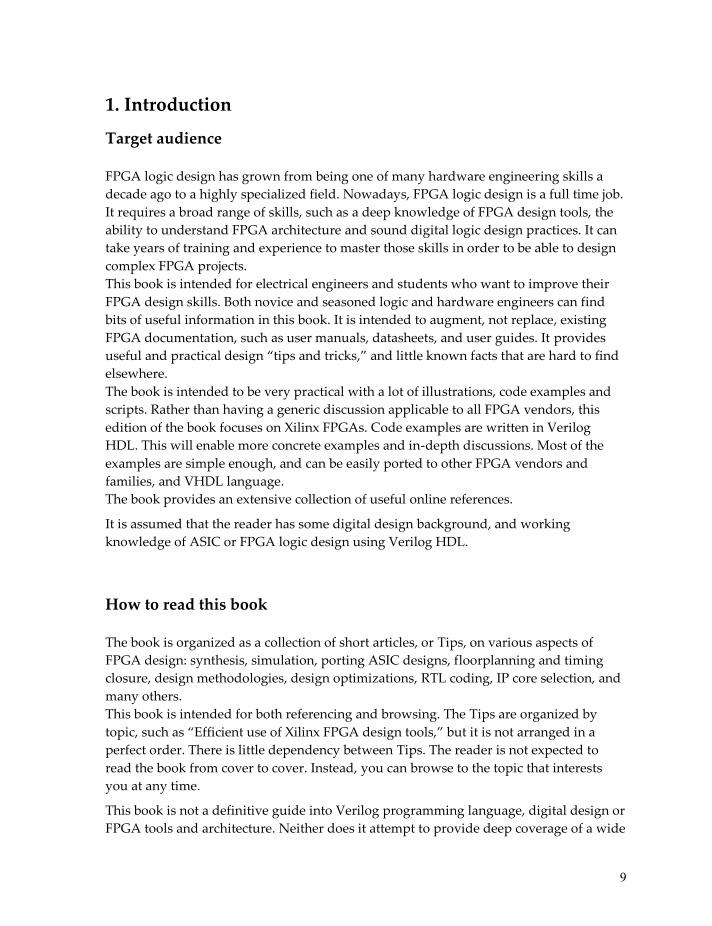
1. Introduction
Target audience
FPGA logic design has grown from being one of many hardware engineering skills a
decade ago to a highly specialized field. Nowadays, FPGA logic design is a full time job.
It requires a broad range of skills, such as a deep knowledge of FPGA design tools, the
ability to understand FPGA architecture and sound digital logic design practices. It can
take years of training and experience to master those skills in order to be able to design
complex FPGA projects.
This book is intended for electrical engineers and students who want to improve their
FPGA design skills. Both novice and seasoned logic and hardware engineers can find
bits of useful information in this book. It is intended to augment, not replace, existing
FPGA documentation, such as user manuals, datasheets, and user guides. It provides
useful and practical design ‚tips and tricks,‛ and little known facts that are hard to find
elsewhere.
The book is intended to be very practical with a lot of illustrations, code examples and
scripts. Rather than having a generic discussion applicable to all FPGA vendors, this
edition of the book focuses on Xilinx FPGAs. Code examples are written in Verilog
HDL. This will enable more concrete examples and in-depth discussions. Most of the
examples are simple enough, and can be easily ported to other FPGA vendors and
families, and VHDL language.
The book provides an extensive collection of useful online references.
It is assumed that the reader has some digital design background, and working
knowledge of ASIC or FPGA logic design using Verilog HDL.
How to read this book
The book is organized as a collection of short articles, or Tips, on various aspects of
FPGA design: synthesis, simulation, porting ASIC designs, floorplanning and timing
closure, design methodologies, design optimizations, RTL coding, IP core selection, and
many others.
This book is intended for both referencing and browsing. The Tips are organized by
topic, such as ‚Efficient use of Xilinx FPGA design tools,‛ but it is not arranged in a
perfect order. There is little dependency between Tips. The reader is not expected to
read the book from cover to cover. Instead, you can browse to the topic that interests
you at any time.
This book is not a definitive guide into Verilog programming language, digital design or
FPGA tools and architecture. Neither does it attempt to provide deep coverage of a wide
Copyright © 2011 Evgeni Stavinov
range of topics in a limited space. Instead, it covers the important points, and provides
references for further exploration of that topic. Some of the material in this book has
appeared previously as more complete articles in technical magazines.
Software
The FPGA synthesis and simulation software used in this book is a free Web edition of
Xilinx ISE package.
Companion web site
An accompanying web site for this book is:
http://outputlogic.com/100_fpga_power_tips
It provides most of the projects, source code, and scripts mentioned in the book. It also
contains links to referenced materials, and errata.
11
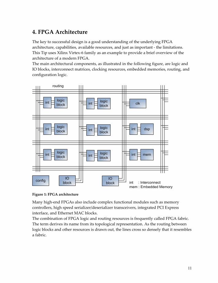
4. FPGA Architecture
The key to successful design is a good understanding of the underlying FPGA
architecture, capabilities, available resources, and just as important - the limitations.
This Tip uses Xilinx Virtex-6 family as an example to provide a brief overview of the
architecture of a modern FPGA.
The main architectural components, as illustrated in the following figure, are logic and
IO blocks, interconnect matrices, clocking resources, embedded memories, routing, and
configuration logic.
Figure 1: FPGA architecture
Many high-end FPGAs also include complex functional modules such as memory
controllers, high speed serializer/deserializer transceivers, integrated PCI Express
interface, and Ethernet MAC blocks.
The combination of FPGA logic and routing resources is frequently called FPGA fabric.
The term derives its name from its topological representation. As the routing between
logic blocks and other resources is drawn out, the lines cross so densely that it resembles
a fabric.
Copyright © 2011 Evgeni Stavinov
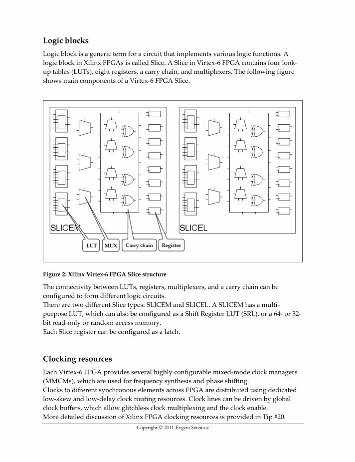
Logic blocks
Logic block is a generic term for a circuit that implements various logic functions. A
logic block in Xilinx FPGAs is called Slice. A Slice in Virtex-6 FPGA contains four look-
up tables (LUTs), eight registers, a carry chain, and multiplexers. The following figure
shows main components of a Virtex-6 FPGA Slice.
Figure 2: Xilinx Virtex-6 FPGA Slice structure
The connectivity between LUTs, registers, multiplexers, and a carry chain can be
configured to form different logic circuits.
There are two different Slice types: SLICEM and SLICEL. A SLICEM has a multi-
purpose LUT, which can also be configured as a Shift Register LUT (SRL), or a 64- or 32-
bit read-only or random access memory.
Each Slice register can be configured as a latch.
Clocking resources
Each Virtex-6 FPGA provides several highly configurable mixed-mode clock managers
(MMCMs), which are used for frequency synthesis and phase shifting.
Clocks to different synchronous elements across FPGA are distributed using dedicated
low-skew and low-delay clock routing resources. Clock lines can be driven by global
clock buffers, which allow glitchless clock multiplexing and the clock enable.
More detailed discussion of Xilinx FPGA clocking resources is provided in Tip #20.
13
Embedded memory
Xilinx FPGAs have two types of embedded memories: a dedicated Block RAM (BRAM)
primitive, and a LUT configured as Distributed RAM
Virtex-6 BRAM can store 36K bits, and can be configured as a single- or dual-ported
RAM. Other configuration options include data width of up to 36-bit, memory depth up
to 32K entries, and error detection and correction.
Tip #34 describes different use cases of FPGA-embedded memory.
DSP
Virtex-6 FPGAs provide dedicated Digital Signal Processing (DSP) primitives to
implement various functions used in DSP applications, such as multipliers,
accumulators, and signed arithmetic operations. The main advantage of using DSP
primitives instead of general-purpose LUTs and registers is high performance.
Tip #28 describes different use cases of DSP primitive.
Input/Output
Input/Output (IO) block enables different IO pin configurations: IO standards, single-
ended or differential, slew rate and the output strength, pull-up or pull-down resistor,
digitally controlled impedance (DCI). An IO in Virtex-6 can be delayed by up to 32
increments of 78 ps each by using an IODELAY primitive.
Serializer/Deserializer
Most of Virtex-6 FPGAs include dedicated transceiver blocks that implement
Serializer/Deserializer (SerDes) circuits. Transceivers can operate at a data rate between
155 Mb/s and 11.18 Gb/s, depending on the configuration.
Routing resources
FPGA routing resources provide programmable connectivity between logic blocks, IOs,
embedded memory, DSP, and other modules. Routing resources are arranged in a
horizontal and vertical grid. A special interconnect module serves as a configurable
switch box to connect logic blocks, IOs, DSP, and other module to horizontal and
vertical routing. Unfortunately, Xilinx doesn’t provide much documentation on
performance characteristics, implementation details, and quantity of the routing
resources. Some routing performance characteristics can be obtained by analyzing
timing reports. And the FPGA Editor tool can be used to glean information about the
routing quantity and structure.
Copyright © 2011 Evgeni Stavinov
FPGA configuration
The majority of modern FPGAs are SRAM-based, including Xilinx Spartan and Virtex
families. On each FPGA power-up, or during a subsequent FPGA reconfiguration, a
bitstream is read from the external non-volatile memory (NVM), processed by the
configuration controller, and loaded to the internal configuration SRAM. Tips #35-37
describe the process of FPGA configuration and bitstream structure in more detail.
The following table summarizes this Tip by showing key features of the smallest, mid-
range, and largest Xilinx Virtex-6 FPGA.
Table 1: Xilinx Virtex-6 FPGA key features
XC6VLX75T XC6VLX240T XC6VLX760
Logic cells 74,496 241,152 758,784
Embedded memory (Kbyte) 832 2,328 4,275
DSP modules 288 768 864
User IOs 240 600 1200
15
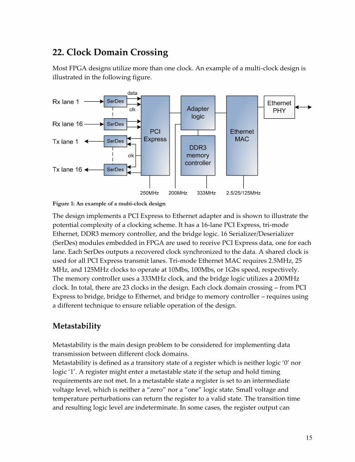
22. Clock Domain Crossing
Most FPGA designs utilize more than one clock. An example of a multi-clock design is
illustrated in the following figure.
Figure 1: An example of a multi-clock design
The design implements a PCI Express to Ethernet adapter and is shown to illustrate the
potential complexity of a clocking scheme. It has a 16-lane PCI Express, tri-mode
Ethernet, DDR3 memory controller, and the bridge logic. 16 Serializer/Deserializer
(SerDes) modules embedded in FPGA are used to receive PCI Express data, one for each
lane. Each SerDes outputs a recovered clock synchronized to the data. A shared clock is
used for all PCI Express transmit lanes. Tri-mode Ethernet MAC requires 2.5MHz, 25
MHz, and 125MHz clocks to operate at 10Mbs, 100Mbs, or 1Gbs speed, respectively.
The memory controller uses a 333MHz clock, and the bridge logic utilizes a 200MHz
clock. In total, there are 23 clocks in the design. Each clock domain crossing – from PCI
Express to bridge, bridge to Ethernet, and bridge to memory controller – requires using
a different technique to ensure reliable operation of the design.
Metastability
Metastability is the main design problem to be considered for implementing data
transmission between different clock domains.
Metastability is defined as a transitory state of a register which is neither logic ‘0’ nor
logic ‘1’. A register might enter a metastable state if the setup and hold timing
requirements are not met. In a metastable state a register is set to an intermediate
voltage level, which is neither a ‚zero‛ nor a ‚one‛ logic state. Small voltage and
temperature perturbations can return the register to a valid state. The transition time
and resulting logic level are indeterminate. In some cases, the register output can
Copyright © 2011 Evgeni Stavinov
oscillate between the two valid states. Metastability conditions arise in designs with
multiple clocks, or asynchronous inputs, and result in data corruption.
The following are some of the circuit examples that can cause metastability.
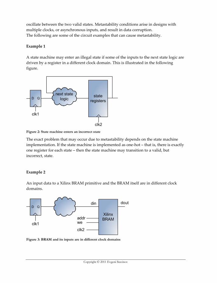
Example 1
A state machine may enter an illegal state if some of the inputs to the next state logic are
driven by a register in a different clock domain. This is illustrated in the following
figure.
Figure 2: State machine enters an incorrect state
The exact problem that may occur due to metastability depends on the state machine
implementation. If the state machine is implemented as one-hot – that is, there is exactly
one register for each state – then the state machine may transition to a valid, but
incorrect, state.
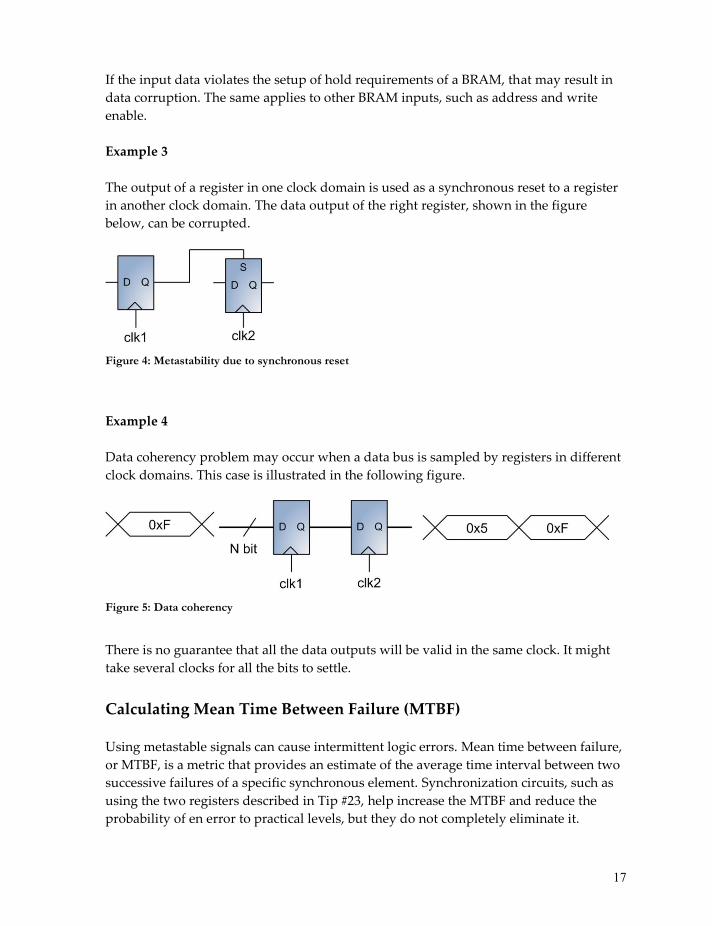
Example 2
An input data to a Xilinx BRAM primitive and the BRAM itself are in different clock
domains.
Figure 3: BRAM and its inputs are in different clock domains
17
If the input data violates the setup of hold requirements of a BRAM, that may result in
data corruption. The same applies to other BRAM inputs, such as address and write
enable.
Example 3
The output of a register in one clock domain is used as a synchronous reset to a register
in another clock domain. The data output of the right register, shown in the figure
below, can be corrupted.
Figure 4: Metastability due to synchronous reset
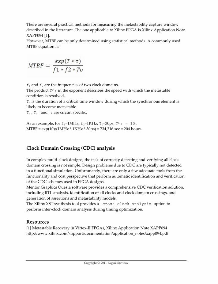
Example 4
Data coherency problem may occur when a data bus is sampled by registers in different
clock domains. This case is illustrated in the following figure.
Figure 5: Data coherency
There is no guarantee that all the data outputs will be valid in the same clock. It might
take several clocks for all the bits to settle.
Calculating Mean Time Between Failure (MTBF)
Using metastable signals can cause intermittent logic errors. Mean time between failure,
or MTBF, is a metric that provides an estimate of the average time interval between two
successive failures of a specific synchronous element. Synchronization circuits, such as
using the two registers described in Tip #23, help increase the MTBF and reduce the
probability of en error to practical levels, but they do not completely eliminate it.
Copyright © 2011 Evgeni Stavinov
There are several practical methods for measuring the metastability capture window
described in the literature. The one applicable to Xilinx FPGA is Xilinx Application Note
XAPP094 [1].
However, MTBF can be only determined using statistical methods. A commonly used
MTBF equation is:
f1 and f2 are the frequencies of two clock domains.
The product T*τ in the exponent describes the speed with which the metastable
condition is resolved.
To is the duration of a critical time window during which the synchronous element is
likely to become metastable.
To , T, and τ are circuit specific.
As an example, for f1=1MHz, f2=1KHz, T0=30ps, T*τ = 10,
MTBF = exp(10)/(1MHz * 1KHz * 30ps) = 734,216 sec = 204 hours.
Clock Domain Crossing (CDC) analysis
In complex multi-clock designs, the task of correctly detecting and verifying all clock
domain crossing is not simple. Design problems due to CDC are typically not detected
in a functional simulation. Unfortunately, there are only a few adequate tools from the
functionality and cost perspective that perform automatic identification and verification
of the CDC schemes used in FPGA designs.
Mentor Graphics Questa software provides a comprehensive CDC verification solution,
including RTL analysis, identification of all clocks and clock domain crossings, and
generation of assertions and metastability models.
The Xilinx XST synthesis tool provides a -cross_clock_analysis option to
perform inter-clock domain analysis during timing optimization.
Resources [1] Metastable Recovery in Virtex-II FPGAs, Xilinx Application Note XAPP094
http://www.xilinx.com/support/documentation/application_notes/xapp094.pdf