Embed Size (px)
Citation preview

Copyright 2007 Society of Photo-Optical Instrumentation Engineers.
This paper was published in SPIE Vol. 6520 (2007) p. 652004, and is made available as an electronic reprint with permission of SPIE. Single print or electronic copies for personal use only are allowed. Systematic or multiple reproduction, or distribution to multiple locations through an electronic listserver or other electronic means, or duplication of any material in this paper for a fee or for commercial purposes is prohibited. By choosing to view or print this document, you agree to all the provisions of the copyright law protecting it.
Optical Lithography … 40 years and holding
John H. Bruning Corning Tropel Corporation
Fairport, NY 14450
ABSTRACT
Optical lithography has been the dominant patterning process for semiconductor fabrication for over 40 years. The patterning process evolved initially from methods used in the printing industry, but as integrated circuits became more complex, and as device geometries shrank, sophisticated new imaging methods evolved. Today’s optical lithography systems represent the highest resolution, most accurate optical imaging systems ever produced. This remarkable evolutionary process continues to this day, paced by “Moore’s Law”. The evolutionary development of lithography systems over the last 40 years is reviewed along with a brief discussion of options for the future. Keywords: lithography history, photolithography, optical lithography, immersion, reduction lithography
1. INTRODUCTION The production of microelectronics has made incredible strides over a period of nearly 50 years. The main driver of lithography improvements is reduced device cost. This has come about through improvements in resolution, resulting in more chips per wafer, higher performance devices, and improvements in productivity, all of which continue to reduce the cost per function in integrated circuits. We review and update an earlier history on this subject from 19971 with a new emphasis on progress in the last 10 years and offer a rationalization for major changes. This paper cannot cover all aspects of the lithography process, but concentrates on the evolution of optical imaging systems and technology.
2. EARLY LITHOGRAPHY
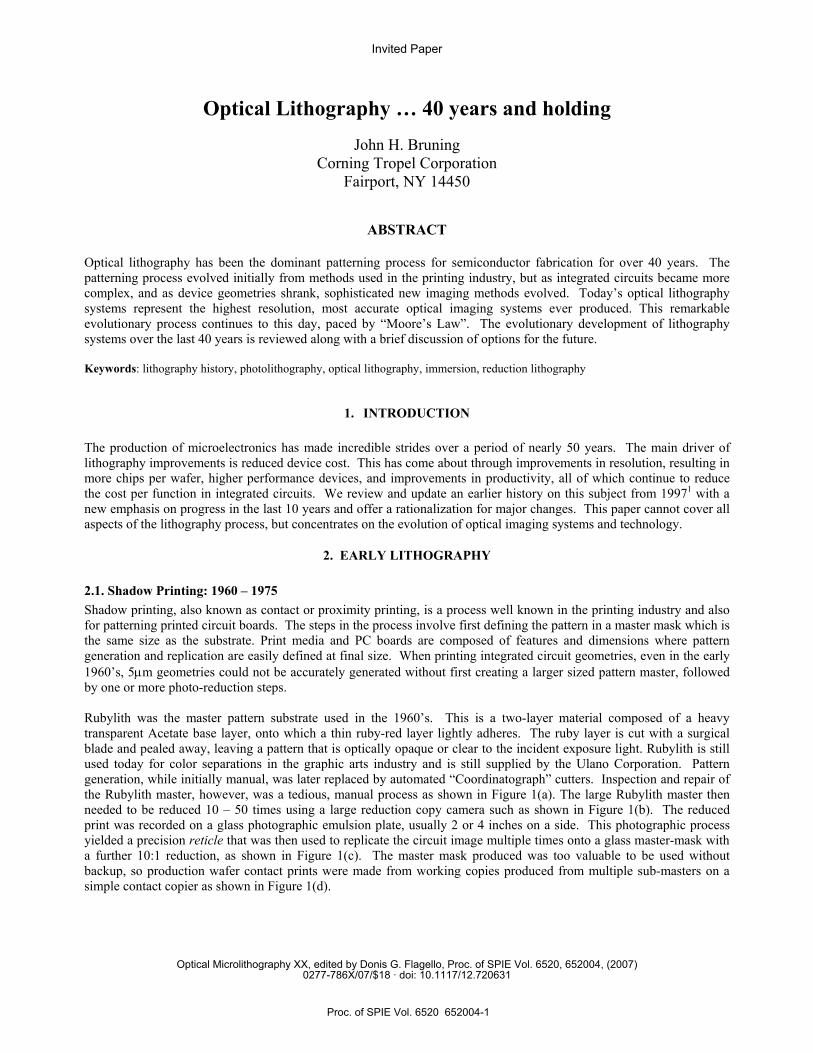
2.1. Shadow Printing: 1960 – 1975 Shadow printing, also known as contact or proximity printing, is a process well known in the printing industry and also for patterning printed circuit boards. The steps in the process involve first defining the pattern in a master mask which is the same size as the substrate. Print media and PC boards are composed of features and dimensions where pattern generation and replication are easily defined at final size. When printing integrated circuit geometries, even in the early 1960’s, 5µm geometries could not be accurately generated without first creating a larger sized pattern master, followed by one or more photo-reduction steps. Rubylith was the master pattern substrate used in the 1960’s. This is a two-layer material composed of a heavy transparent Acetate base layer, onto which a thin ruby-red layer lightly adheres. The ruby layer is cut with a surgical blade and pealed away, leaving a pattern that is optically opaque or clear to the incident exposure light. Rubylith is still used today for color separations in the graphic arts industry and is still supplied by the Ulano Corporation. Pattern generation, while initially manual, was later replaced by automated “Coordinatograph” cutters. Inspection and repair of the Rubylith master, however, was a tedious, manual process as shown in Figure 1(a). The large Rubylith master then needed to be reduced 10 – 50 times using a large reduction copy camera such as shown in Figure 1(b). The reduced print was recorded on a glass photographic emulsion plate, usually 2 or 4 inches on a side. This photographic process yielded a precision reticle that was then used to replicate the circuit image multiple times onto a glass master-mask with a further 10:1 reduction, as shown in Figure 1(c). The master mask produced was too valuable to be used without backup, so production wafer contact prints were made from working copies produced from multiple sub-masters on a simple contact copier as shown in Figure 1(d).
Invited Paper
Optical Microlithography XX, edited by Donis G. Flagello, Proc. of SPIE Vol. 6520, 652004, (2007)0277-786X/07/$18 · doi: 10.1117/12.720631
Proc. of SPIE Vol. 6520 652004-1

A
(a) (b)
(c) (d)
Figure 1. (a) Rubylith master, (b) Reduction copy camera, (c) Step and Repeat Camera, (d) Mask contact copier
2.2. Second Generation Mask-Making: 1970 – 1980 The mask making process described above was really quite clumsy, often combining multiple pieces of equipments from different manufacturers. Some of the larger semiconductor manufacturers made substantial investments to improve the mask making process. One particularly significant effort by Bell Laboratories included development and implementation of an integrated mask making system that included integrated pattern layout and mask management software, a fast laser pattern generator, reduction camera and step-and-repeat camera for the creation of master masks2. Three such pieces of equipment are shown in Figure 2. The Primary Pattern Generator, shown in Figure 2(a) used a single-mode Argon Laser operating at 514nm with external acousto-optic modulation at 2 MHz. The 26,000 pixel, 32,000 line primary pattern was recorded in photographic emulsion on an 8” x 10” x ¼” Kodak High Resolution Plate (HRP). A 7um Gaussian spot was scanned by a rotating 10-sided polygon and scan lens, optically corrected for constant spot-size and exposure along the scan-line. A precision step-motor and ball-screw advanced the plate, perpendicular to the scan-line in 7um increments during the dead-time between facets. 5 spots, or address units, made up a minimum width line on the plate. Figure 2(b) shows a precision reduction camera, operating at a reduction ratio of 3.5:1. The function of this camera was to produce a reduced image reticle from the 8” x 10” primary pattern plate onto a 4” x 5” HRP for use at a later step. The camera lens and illuminator were highly corrected for distortion, uniformity of imagery, and uniformity of illumination intensity over the image field. The address size at the reticle was 2µm and the minimum feature-width was 10µm. The reticle so produced served as the input to a 10:1 reduction step-and-repeat camera shown in Figure 2(c). Using this reticle, the step-and-repeat camera photo-composed a finished 1:1 master with an address size of 0.2µm and a minimum feature size or critical dimension, CD, of 1.0µm. The maximum image or chip-size was 5mm x 5mm, but multiple patterns could be arrayed onto a plate up to 100mm x 100mm. This pattern array was then used as a master for contact or projection printing onto wafers 85mm diameter or less. A mask from this period is shown in Figure 2(d).
Proc. of SPIE Vol. 6520 652004-2

• •IiI I
1Il
•1 * —
(a) (b)
(c) (d)
Figure 2. (a) Primary Pattern Generator, (b) 3.5x Reduction Camera, (c) Step-and-Repeat Camera, (d) Master Mask
2.3. Projection Printing: 1970 – 1985 One of the obvious problems with contact printing is the inevitable damage to the wafer by contact and the cumulative damage to the mask with each additional contact. While contact printing is a simple process, projection printing is deceptively complex. Initially, projection printing was done with a custom 1:1 imaging lens between the mask and wafer when 2” diameter wafers were the norm. But even at this field size, the optical challenges were great. Several refractive lens systems built by Canon, Telefunken and others, demonstrated instabilities associated with long air paths, optical glasses with high absorption and poor homogeneity, rendering these systems unworthy for production1. The next generation of 1:1 systems was based on a unique concentric lens design invented by Dyson3. Variations on this design gave a larger working distance and overcame the problem that object and image shared the same space. The Dyson relay is catadioptric, incorporating both refractive and reflective components. Systems based on this concept, such as one by Optimetrix shown in Figure 3, were ultimately plagued by some of the same issues that limited performance of earlier 1:1 full-wafer dioptric or all-refractive systems. The transition of wafer size from 50mm to 75mm put a greater burden on layer to layer overlay, which was compounded by further improvements in resolution. A rule of thumb then, and now, is that layer-to-layer overlay error should be 20% of the minimum CD or less. This became a more serious issue with larger wafers due to differential expansion between the mask and wafer, differing film stresses on the wafer, changes in lens distortion during exposure and mismatches in lens distortion from tool-to-tool. During the mid 1970’s optically based mask generation tools began to reach their limits because 1:1 masks needed to grow in size to match the larger wafers. This trend continued until wafers reached 6” in diameter. This capped the growth of masks to 6” x 6”. 1:1 masks were preferentially produced by e-beam at final dimensions on 6” substrates. This eliminated the need to make more than a single mask or reticle substrate for wafer exposure. Bell Laboratories developed three generations of successful electron beam exposure systems called EBES4. These were licensed and successfully commercialized in the early 1980’s.
Proc. of SPIE Vol. 6520 652004-3

Mask
Warer
Fall Wf I[gi[g75 mm 4,fleld
?=436,NA=0.2W 1,8 i, N 3.4 x 10⁸
M3
I N /4 M4
Arc Illumination Roof-Mirror Plane-Mirror
Mask Wafer
Mask and Wafer pivot as a unitabout the scan axis
Figure 3. Optimetrix 1:1 full wafer printer for 75mm wafers (1974)
Economic pressures eventually drove device makers to larger wafers, higher resolution and higher throughput, which in turn drove optical designers toward more stable imaging systems with greater control of overlay. In 1970, the Perkin-Elmer Corporation introduced a novel all-reflective (catoptric), 1:1 scanning system that changed the lithography landscape for more than a decade. This new exposure system, the Micralign 100, was based on the Offner relay5, an elegant and simple 1:1 imaging system composed of two concentric spherical mirrors and three plane fold mirrors to bring object and image planes into useful positions. This system is shown in Figure 4.
Figure 4. Perkin Elmer Micralign 100 (1974)
The optical simplicity of the system is evident, but making it work relied on superb figure, proper assembly and alignment of all mirrors, along with a high precision scanning carriage. The optical system has a perfectly flat image field because of its zero Petzval sum. The large concave mirror is used twice, while the smaller convex mirror with twice the curvature, is used only once. This unique system is also telecentric in both object and image spaces. The numerical aperture of the system is, however, restricted by vignetting to no more than 0.16. The image is well corrected only over a narrow annular width of 1mm when the median diameter of the annulus is 150mm. The lens is illuminated by a high-pressure Hg capillary lamp bent into a circular arc, whose image on the wafer has a cord length equal to the wafer diameter. The illuminator, its circular segment image of the arc, and the imaging lens are stationary. A carriage supporting the mask and wafer in parallel planes, is pivoted about an axis parallel to a line joining the centers of the mask and wafer. Axial symmetry of the optical design theoretically provides uniform imagery along the annulus, which when combined with scanning, nominally perpendicular to the chord of the annular segment, provided very uniform imagery over the full extent of the wafer, without a “sweet-spot”. Several competitive systems, with the minor variations shown in Figures 5 and 6, were legally blocked and appeared on the market only briefly.
Proc. of SPIE Vol. 6520 652004-4

3,Arc Illumination
Mask
VVater
Scan
Directionor Scan
MS
Mask Wafer
Mask
Dyson
Wafer
IlluminationSource
Figure 5. Canon MPA-500FA (1978) Figure 6. Cobilt CA 3000 (1978) A larger, final evolution of the Micralign is shown in Figure 7. This system, commercialized in 1984, had no fold mirrors, but an annular field large enough to sweep out a 6” wafer.
Figure 7. Perkin Elmer Micralign 500 (1984)
Several other approaches to 1:1 printing were attempted with varying degrees of success. The Micralign systems were ultimately limited by overlay, primarily because there were few practical methods to compensate overlay errors over a large wafer. In 1976, Bell Laboratories developed several prototypes of a 2-dimensional Scanning Projection Printer6 (SPP) as shown in Figure 8.
Figure 8. Bell Labs 1:1 Scanning projection printer (1976)
Proc. of SPIE Vol. 6520 652004-5

aHg Arc Lamp-house ______ Reticle AlignmentMicroscope
I-— Cast Iron Optical Column
Laser Interferometer 10:1 Zeiss LensNA= 0.28
water Alignment
water Stage Microscope2-point Aug nment
This system was also based on the Dyson relay which is capable of considerably higher NA than the Offner relay, but only realized when object and image are on or close to the optical axis. Here, object and image, while optically on-axis, were physically separated by approximately 8” by using polarized illumination, a polarization beam-splitter and a quarter-wave plate at the concave mirror. The complex prism arrangement separates and orients the object and image onto a single flat plane, so that the scanned image transfers to the wafer without blur. The diamond-shaped image overlaps on adjacent scans. Provision for small motions of the mask during exposure allowed for small overlay corrections. The system never worked properly due to pattern dependent, thermally induced aberrations resulting from high optical absorption in long glass paths. A novel fix was found by scaling down the optical system, re-plumbing object and image locations, and changing the optical material to low-loss fused silica7. This was never implemented because more economical stepper-based solutions became available. One such solution was a 1:1 stepper commercialized by Ultratech Stepper in 1980. The imaging lens was based, once again, on the simple Dyson relay. This approach did not require a beam-splitter or polarized light since it used an off-axis image. The off-axis object and image fields were cleverly separated by compact prisms8. This approach evolved to increasingly larger fields and NA9. This stepper configuration struggled in the marketplace, in part, because it required non-standard masks, pellicles, inspection and support equipment. Within the same time period, reduction steppers gained rapid acceptance because of improved CD control at the wafer and the greatly reduced burden on the mask-maker. This relatively brief period was regarded as a “mask-makers holiday”.
3. REDUCTION LITHOGRAPHY The maturing mask-making process enabled reduction photolithography directly onto the wafer since it was nearly identical to the last lithography step in the production of 1:1 photomasks. Printing a reduced image of the reticle directly onto the wafer required the addition of a wafer alignment step, but eliminated making a 1:1 mask all together. The GCA Corporation, having previously produced reduction photo-repeaters for mask-making, redesigned the product to align and step the reduced image directly onto the wafer. The first wafer stepper, the 4800 DSW, was introduced in 1978 and is shown in Figure 9. It was the first such product to utilize automated wafer handling and alignment. The reduction lens, made by Carl Zeiss, had a 10:1 reduction ratio, a numerical aperture of 0.28 and a field size of 10mm x 10mm. The exposure wavelength was the spectrally isolated mercury g-line (436nm) from a high-pressure mercury lamp. Zeiss supplied a variety of lenses prior to GCA acquiring Tropel as a captive lens supplier.
Figure 9. GCA 4800 DSW 10:1 Reduction Stepper
Proc. of SPIE Vol. 6520 652004-6

H
9
3.1. Reduction stepper lens evolution: 1980 - 1993 A few useful figures of merit for lithographic lenses are resolution and pixel count. We define resolution as the minimum printable critical-dimension, minCD , as:
NAkCD λ1min ≈ , (1)
where k1 is a process dependent factor in the range .3 < k1 < 1. Thus, resolution improves when k1 or λ are reduced, or when the numerical aperture, NA, is increased. Pixel count, N, is defined as the number of pixels of size minCD x
minCD that fit within the useful image field, imageA , or:
2minCD
AN image≈ . (2)
Lenses with axial symmetry naturally print a circular field, but wafer-stepper reticles are typically 150mm square, with the central 130mm square available for device patterns. Lithography tool productivity increases when the stepper image size increases due to fewer exposures per wafer. Higher resolution means more circuits per wafer and higher performance chips. Initially, wafer steppers imaged reticles with a 10:1 reduction. As chip-size requirements grew, reduction ratios were reduced so that larger chips, or larger blocks of chips, could be imaged with the same reticle substrate size. Table 1 summarizes some of critical change points in reduction-ratio, wafer size and field size.
Table 1. Turning points in reduction wafer stepper evolution
Year Reduction Wafer Dia. (mm) Image Area (mm x mm) λ (nm) CDmin N 1970 1:1 50 50mm dia. full-wafer 400 – 440 lamp 5.0um 7.9 x 10⁷ 1980 10:1 100 10mm x 10mm 436 1.5um 4.4 x 10⁷ 1985 5:1 150 14mm x 14mm 436 1.0um 2.0 x 10⁸ 1990 4:1 200 20mm x 20mm 365 0.5um 1.7 x 10⁹ 1993 4:1 200 22mm x 22mm 248 .25um 7.7 x 10⁹
Note the dramatic increase in N over time, image area and minCD . Note also that the burden on the lens manufacturer was initially reduced when the industry moved from full-wafer imaging to reduction step-and-repeat, but as the need for higher resolution and image area grew, dramatic increases in lens size and complexity were required. Lens cross-sections representative of the period in Table 1, produced by Tropel, are shown in Figure 10. Less evident from the Figure are changes that took place in wavelength, sources, and materials to achieve these advances in resolution, field size and complexity. This development spanned nearly 20 years until GCA exited the stepper business in 1993.
Figure 10. GCA/Tropel lithographic lenses 1965 – 1993
Proc. of SPIE Vol. 6520 652004-7

Annular Field
i'J_22-C" 32
,Image Wafer Plane
3.2. High-NA step-and-scan reduction lithography: 1990 – 2004 Demand for still-higher resolution and throughput drove lithography tool makers to further enlarge the image field by stepping and scanning the image. Scanning afforded the opportunity to increase image field coverage without increasing the natural field size of the lens. In 1990, Perkin Elmer introduced the first step-and-scan system, the Micrascan I10. This system had an annular image field, but a complex optical system with many folds, as shown in Figure 11. This system was very difficult to manufacture. Three years later, the system was replaced by the SVGL Micrascan II, shown in Figure 12. The MS-II design was a more manufacturable folded catadioptric design that enabled scanning a narrow, rectangular strip image which reduced the throughput loss from over-scanning an annular image field. Multiple generations of the Micrascan are summarized in Table 2 and reference 11.
Figure 11. Micrascan I (1990) Figure 12. Micrascan II (1993)
Table 2. Evolution of PE/SVGL Micrascan step-and-scan systems (1990 – 2003)
Ultimately, the size and homogeneity requirements of the large beamsplitter cube limited the highest attainable NA. The MS-VII, while a significant technical achievement, never advanced beyond the prototype stage, due to the limited availability of high-purity CaF2 and other issues associated with pellicles and resist. It took little time for the other lithography manufacturers, ASML/Zeiss, Canon and Nikon, to realize that the same all-refractive lens technology used for wafer stepping was well suited for step-and-scan lithography. In fact, a refractive stepper lens, with its circular image field, can scan an image field nearly 30% larger in height than the inscribed square. This results because the scanning aperture can be nearly equal to the full diameter of the circular image field. This is a great advantage since larger image fields can be exposed by smaller lenses, or same-sized lenses of higher numerical aperture. The trade-off of reduced lens size and cost at the expense of increased stage cost and complexity has enabled significantly higher NA lenses to be implemented. This can be seen in Figure 13 and Table 3, where lenses from Nikon are shown in cross-section, spanning the period from 1982 to 200412. Many things changed between lens generations, including wavelength, field-size and resolution. These changes had a dramatic effect on lens size, cost and complexity. Consider, for example, the consequences of changing the wavelength from 365nm in the stepper lens of 1993, to 248nm in the scanner lens of 1999. Changing the illumination source from a lamp to an excimer laser required a change of optical materials, a change of photoresist materials, chemistry and processes, as well as the development of improved tools, metrology and processes for lens manufacturing. The relatively large 3nm bandwidth of the Hg i-line required
Year Model Image Area (mm x mm) λ (nm) NA CDmin(nm) N 1990 MS-I 22mm x 32mm - Annular 250 lamp 0.35 350 5.6 x 10⁹ 1993 MS-II 26mm x 50mm - Strip 250 lamp 0.50 250 2.1 x 10¹⁰ 1997 MS-III 26mm x 50mm - Strip 248 KrF 0.60 200 3.2 x 10¹⁰ 2001 MS-V 26mm x 50mm - Strip 193 ArF 0.75 130 7.7 x 10¹⁰ 2003 MS-VII 26mm x 50mm - Strip 157 F2 0.75 100 1.3 x 10¹¹
Proc. of SPIE Vol. 6520 652004-8

a- a a
multiple glasses to correct color aberrations over this large spectral bandwidth (as with earlier g-line lenses). Changing the source to a line-narrowed, 248nm KrF excimer laser, eliminated the need to color correct the lens13. As a result, the few-pm source bandwidth allowed all elements of the lens to be made from fused silica, an optimized material for the ultraviolet. The rapid development of excimer lasers for lithography is an impressive story unto its own14. Compare next the 2004 and 1999 lenses from Figure 13 and Table 3. The 2004 lens was designed to work at the 193nm wavelength of the ArF excimer laser. This wavelength change once again required new photoresists, chemistry and processes. The huge NA increase from .68 to .85 was accomplished with a relatively small increase in physical size in order to avoid a larger increase in cost and complexity. This came about through the introduction of large departure aspheric surfaces into the design, which substantially changed the optical design form from the predecessor lenses12.
1982 1989 1993 1999 2004
Figure 13. Nikon lithography lenses
Table 3.
3.3. Ultra-high NA and immersion imaging (2003 – Present) In early 2000, lithography faced an even greater challenge keeping up with Moore’s Law. Both 157nm and 193nm wavelengths were being developed along with other optical and non-optical approaches with no obvious long-term choice. By 2003, 157nm was written off as an impractical next step in optical lithography after 193nm. Optical lithography demonstrated tremendous staying power and accumulated an enormous investment in its supporting infrastructure and technologies. Besides advancements in wavelength and numerical aperture, further resolution improvements have come about as a result of improved mask, wafer and process integration that allow lithography systems to operate at smaller values of k1. Figure 14 illustrates the progress in exploiting optical lithography at lower k1 values over a period of nearly 15 years15. The cross-features with their overlayed aerial images to the right of the Figure show the impact on the aerial image when the cross feature is printed, at that particular k1 value, without compensation or resolution extension techniques.
Year Image Area (mm x mm) λ (nm) NA CDmin(nm) N 1982 15mm x 15mm - Stepper 436 lamp 0.30 1200 1.6 x 10⁸ 1989 15mm x 15mm - Stepper 435 lamp 0.54 660 5.2 x 10⁸ 1993 22mm x 22mm - Stepper 365 lamp 0.57 450 2.4 x 10⁹ 1999 26mm x 32mm - Scanner 248 KrF 0.68 200 2.1 x 10¹⁰ 2004 26mm x 32mm - Scanner 193 ArF 0.85 82 1.2 x 10¹¹
Proc. of SPIE Vol. 6520 652004-9

0.9 350nm nodeA
0.85O0nr node
Wavelength0.7 N
'365N A245
0.6250nm node
Al8Onm node • 157
0.5 A
9Onm node
• 193
l3Onm node OSnn node0.4
65nm nod0.3
1992 1994 1996 1998 2000 2002 2004 2006
Figure 14. Historical trend of k1 and its effect on the resist image without compensation
Operating at lower k1 values requires superb uniformity of imaging, uniformity of illumination, and uniformity of image placement, to nanometer levels. While lens designers achieve near-zero aberration targets, at the design stage, realizing design performance requires nearly perfect materials and processes. Optical elements must be fabricated from material that is homogeneous in index to fraction ppm, birefringence free and low in absorption. High purity fused silica is an optimized UV optical material for this application and material improvements continue to evolve. Lens element polishing, coating and metrology processes must also approach perfection. Finally, lens element mounts and the assembly structure, must be precise, kinematic, and stable, with no discernable deformation to components or surfaces. In a production environment, it is particularly important that the lithographic lenses and tool platforms match one another, particularly in image placement and CD control, within the image field and across the wafer. Achieving such high performance and uniformity between tools requires aberration correction 5-10x better than the traditional definitions of the “diffraction limit”, such as the Marechal Criterion12. Once the lens and illumination system are operational within in the exposure tool, there are many other fine “tweaks”, some static, others dynamic, that must be made to various components to maintain performance and matching. Many parameters and characteristics are under dynamic control including focus, exposure, magnification, temperature, laser power, wavelength, and bandwidth, including some lens characteristics, to name a few. Other examples include dynamic infrared thermal aberration control12, control of polarization induced aberrations12, in-situ lens interferometry15, and fine motion control of multiple components in the optical system15. Wafer exposure by scanning a slit image, allows sophisticated tracking of non-flat mask and wafer surfaces, which permits greater image fidelity and process tolerance than possible with static imaging16. It is truly amazing that such precise imagery and image placement can result when reticle and wafer are moving at such high speeds and different speeds. Decades earlier, it was unthinkable to change device processes for lithography reasons. Process changes were the turf of material scientists, device physicists and circuit designers. Today, device improvements are more difficult and convoluted, requiring not only greater resolution, but greater system thinking and design for manufacturability. Lithographic specific processes improvements such as antireflection from the top and bottom surfaces of the resist18 proved improved device yields. Planarization techniques using CMP, shown in Figure 14(b), have become standard in device processing17 and enable devices to work over the very narrow working depth of focus at high yield for optics with NA ≈ 1. This should enable 193nm water-immersion lithography at even higher NA of ≈ 1.3. In this arena, depth of focus is practically limited to ≈λ/2 or 100nm for 193nm tools. Today’s steppers would have very poor yield with the older, unplanarized processes17 shown in Figure 14(a).
Proc. of SPIE Vol. 6520 652004-10

i 1A
'WI )(
I' t*
' Mt
—S
(a) (b)
Figure 14. Unlike older processes (a), modern CMP processes planarize the wafer at nearly every lithography step (b)
Other improvements that enable low-k1 lithography include modified illumination techniques19, resolution enhancement techniques (RET) and optical proximity correction (OPC). These techniques are able to simulate realistic mask structures and provide guidance as to how mask structures can be modified to produce images closer to the desired image shapes19. As resolution extension techniques become more extreme, mask and wafer patterns become physically less and less alike.
3.4 Immersion Lithography Water-immersion lithography at 193nm, in principal, allows the NA to rise to nearly 1.4, but the lens design problem is very challenging. Simple morphing of a lower index dioptric design to higher NA has been shown to be economically and technically impractical20. Catadioptric design forms, however, were found to be essential in order to contain size and cost while keeping the image field flat20, 21. Catadioptric lenses are particularly difficult to design because the multiple mirror surfaces tend to obscure one another. The best lens designs smoothly distribute ray bending among the many optical surfaces in a lens system. Strong refractions introduce large aberrations that must be compensated elsewhere in the lens, so it is best to avoid them when possible. Analogously for reflecting surfaces, reflections close to normal incidence create the least problems, but then they are more likely to obscure one another unless they are widely separated – hence the difficulties. (a) Dioptric (b) In-line Catadioptric (c) Folded Catadioptric
Figure 15. Comparison of immersion lens design forms for NA=1.2
Proc. of SPIE Vol. 6520 652004-11

The problem and two representative solutions are illustrated in the Figure 15 above20. Figure 15(a) shows a dioptric solution for an immersion lens at NA = 1.2. In comparison to lower NA counterparts, (cf. Fig. 10 and 13) elements of this hyper-NA lens become unavoidably large, thick, and strongly refracting in the journey from a lower to an NA = 1.2, while keeping the image field flat. If well placed mirrors of appropriate power are able to do some of the work, more “relaxed” designs can results. The in-line design of Zeiss20 shown in Figure 15(b) is an elegant solution in that there are few strong refractions or reflections and the construction remains a centered, on-axis optical system. The folded design of Figure 15(c) is similarly relaxed, except for the fold mirrors which break axial symmetry of the main optical path. Both lens design forms shown in Figures 15(b) and 15(c) appear to be able to be migrated to higher NA’s. Innovation in UV lithography has been very rapid, particularly at the 193nm wavelength. Figure 16 and Table 4 show the evolution of 193nm scanner lenses in size, resolution and NA developed by ASML/ Zeiss22. These lenses cover a common field size of 26mm x 32mm and span both air (dry) and immersion (wet) imaging.
Figure 16. 193nm lens evolution at Carl Zeiss
Table 4. Parameters of Zeiss Lens
Model 900 1100 1200 1400 1700 1900 Node, CDmin 130 100 80 65 50 45
NA .63 .75 .85 .93 1.20 1.35 k1 Factor .42 .39 .35 .31 .31 .31
N 4.9 x 10¹⁰ 8.3 x 10¹⁰ 1.3 x 10¹¹ 2.0 x 10¹¹ 3.3 x 10¹¹ 4.1 x 10¹¹
4. Conclusions and Outlook The great economic value and industry pressure to continue incremental improvements in optical lithography has always been underestimated. But industry competition, cooperation and customer-pull for improvements have a way of making difficult things work. Where optical lithography will be in 10 years is not clear, other than that it will still be the primary lithographic technology for production. Barriers to continued optical lithography improvement already visible, surmounting those barriers may become practical for reasons we cannot yet see. The following issues will likely keep optics as the dominant lithographic technology for the foreseeable future. Double Patterning Technology is rapidly emerging as the most viable next optical patterning method and has demonstrated imaging at a k1 value of 0.1424. This technology requires process optimization with conventional tools, is clumsy and requires more exposures per wafer level which lowers productivity and raises costs. The semiconductor industry tends to adopt new approaches when they are needed and there are no other viable alternatives. If higher-index optical materials and resists are developed for immersion lenses, numerical apertures could be pushed beyond NA = 1.5 and lens sizes could be reduced. Such new material is only needed for the optical element closest to the wafer23.
Proc. of SPIE Vol. 6520 652004-12

The effective “pixel-rate” of optical lithography is and has been the highest of any lithography technology and is still growing. A 45nm node, 193nm immersion scanner exposing 300mm wafers at 100 wafers per hour has a pixel exposure rate of approximately 1015 Pixels/sec or approximately 1017 bits/sec! It is currently inconceivable that this exposure rate could be exceeded by any other means. Maskless exposure with high density spatial light modulators (SLM) could work with a small-field, high reduction, 2D scanning system. Such a high reduction, small-field lens could be made considerably better than today’s nearly perfect 4:1 large-field lenses. SLM technology and high bandwidth electronics are improving rapidly, but it has a long way to go to catch up with the pixel exposure rate above. Eliminating the mask is likely to change the cost model in a way that is difficult to quantify, but may be attractive. This would likely be a tool that could easily mix with more conventional optical lithography tools. If field-size can be compromised (i.e. reduced), further improvements in lenses with better overlay could be made. Two-dimensional scanning with a smaller-field lens may have merit. The next factor of two improvement in resolution could take many potential paths before arrival, but is nonetheless, very likely to occur. In any event, optical lithography is still the most productive and flexible lithographic technology. That fact alone should guarantee survival for the foreseeable future.
Acknowledgements The author wishes to thank the following people and organizations for generously providing graphic material and assistance: Donis Flagello of ASML, Akiyoshi Suzuki and Phil Ware, Canon Inc., David Williamson and Tomoyuki Matsuyama of Nikon Corporation, Winfried Kaiser of Carl Zeiss, Tim Brunner of IBM, Bob Sell and Dave Young of Corning.
References 1. J. Bruning, Optical Lithography – Thirty years and three orders of magnitude, Proc. SPIE, 3050, (1997) 2. K. Poole, Bell System Technical Journal, November (1970) 3. J. Dyson, "Unit magnification optical system without Seidel aberrations", J. Opt. Soc. Am., 49, p. 713, 1959 4. D. Alles, et. al., “EBES, A practical electron lithographic system”, IEEE Trans. Electron Devices, ED-22, (1975) 5. A. Offner, "New concepts in projection mask aligners", Opt. Eng. 14(2), pp. 130-132, 1975. 6. M. King, et. al., “A scanning projection printer”, Appl. Opt., (1978) 7. J. Bruning, A. White, Patent No. 4171870, Compact image projection apparatus, 1979 9. H. Jeong, et. al., "Optical projection system for gigabit random access memories", JVST, 49, p. 713, 1995 10. J. Buckley, “Step-and-scan: A systems overview of a new lithography tool”, Proc. SPIE, 1088 (1989) 11. D. Williamson, “DUV or EUV, that is the question”, Proc. SPIE, 4146, (2000) 12. Matsuyama, et. al., “Lithographic lens: its history and evolution”, SPIE Microlithography, 2006 13. J. Bruning, Patent No. 4,773,750, Deep-UV Lithography, 1988 14. G. Blumenstock, “Lithography light sources through 2010”, Cymer 11/20/2006 15. P. Ware, “Pushing ArF to the limits”, DNS Lithography Breakfast Forum, 2003 16. A.Namba, et. al., “0.85NA ArF scanner: advancing features and performances“, Proc. SPIE 5377 (2004) 17. T. Brunner, “Lithography technology for 45nm CMOS”, MIT Technical Symposium, 3-8-2005 18. T.A. Brunner, "Optimization of optical properties of photoresist processes", SPIE 1466 p. 297 (1991) 19. A. Wong, “Resolution Enhancement Techniques in Optical Lithography”, SPIE Press (2001). 20. B. Kneer, et. al., “Catadioptric Lens Design: The Breakthrough to Hyper-NA Optics”, Proc. SPIE, 6154-20 (2006) 21. H. Ikezawa, et. al., “A Hyper-NA Projection Lens for ArF Immersion Exposure Tool”, Proc. SPIE, 6154-21, (2006) 22. W. Kaiser, Carl Zeiss SMT, (2007) 23. A.Suzuki: “Critical issues of high index materials”, High Index Materials Critical Review, Kyoto Meeting (2006) 24. M. Levinson, “Double double, toil and trouble”, Microlithography World, article 286361 (2007)
Proc. of SPIE Vol. 6520 652004-13