Embed Size (px)
Citation preview

DC ANALYSIS OF QUASI-RESONANT BUCK AND FORWARDCONVERTERS INCLUDING EFFECTS OF PARASITIC ELEMENTS
bvLEWIS MARLIN ROUFBERG
Thesis submitted to the Faculty 0F the
Virginia Polytechnic Institute and State Universityin partial Fulfillment 0F the requirements For the degree 0F
MASTER OF SCIENCEin
ELECTRICAL ENGINEERING
APPROVED:
1 Fred C. Läe, Chairman
Vatche Voréerian Cho
March, 1987Blacksburg, Virginia

DC ANALYSIS OF QUASI-RESONANT BUCK AND FORWARDCONVERTERS INCLUDING EFFECTS OF PARASITIC ELEMENTS
by i
LEWIS MARLIN ROUFBERG
Fred C. Lee, Chairman
ELECTRICAL ENGINEERING
(ABSTRACT)
The need for smaller and more efficient power supplies steadily grows. Many power supplies in-
corporate high-frequency dc·to—dc switching converters to meet these demands. Recently, a new
class of switching converters has been introduced which can operate at very high frequencies to
further reduce size and increase efficiency. They are called quasi-resonant converters. Previously,
the dc characteristics of many of these converters had been determined, assuming ideal components
and circuit operating conditions. However, as the frequency of operation increases, the circuit be-
havior becomes less ideal causing changes in the expected characteristics. This is because resistive
losses, sexniconductor junction capacitances, and other parasitic (undesirable) elements become
more pronounced at higher frequencies.
This thesis investigates the effects of parasitic elements on the dc characteristics of several zero-
current-switched, buck-derived quasi-resonant converters. For the quasi-resonant buck converter,
it is demonstrated that for certain operating conditions the dc voltage gain can increase when
parasitic losses are increased. Design guidelines are given for maximizing this converter’s efficiency.Various forward quasi~resonant topologies are investigated, and the effects of parasitic elements on
circuit operation are highlighted. A dc analysis is performed for the secondaxy-resonance forward
converter, which has not previously been analyzed. This converter can operate either in full-wave
or half-wave mode. Its dc voltage gain in full-wave mode is less sensitive to load variations than {other resonant forward topologies that only operate in ha1f·wave mode. {
II
I

l
Acknowledgements
I I thank my advisor, Dr. Fred C. Lee, for his support, skillful guidance, and encouragement during
my research. I have greatly enjoyed the opportunity to work with and learn from him.
I am grateful to my cormnittee members: Dr. Vatche Vorperian, for directing the theoretical anal-ysis in my research; and Dr. Bo H. Cho, for many helpful discussions and suggestions.
It has been a pleasure associating with the excellent faculty, staff, and students at the Virginia PowerElectronics Center (VPEC). I thank all the VPEC members who, each in their own way, has en-
riched my experience.
This research was supported in part by the International Business Machines Corporation,Lexington, Kentucky, under contract number 85-1119-02 and in part by the VPEC Industry-
University Partnership Program.
Acknowledgements iii

I
I
Table of Contents1. INTRODUCTION ..................................................... 11.1 Background Information ................................................ 11.2 Preview of Material lncluded in this Thesis ................................... 51.3 IGSPICE Circuit Simulation Program and Component Models .................... 81.4 Terminology ........................................................ 13
2. 'IHE QUASI-RESONANT BUCK CONVERTER ............................. 17
2.1 Review of Ideal Circuit Operation and DC Characteristics ....................... 172.1.1 Ideal Circuit Operation ............................................. 172.1.2 DC Voltage Gain for the Lossless Buck QRC ............................. 22
2.2 DC Voltage Gain and Efficiency for the Buck QRC With Losses .................. 242.3 Effect of Losses on the Buck QRC Resonant Tank Waveforms ................... 28
2.4 Simple, Approximate Expressions to Predict DC Voltage Gain and Efiiciency ......... 302.5 Design Guidelines to Maximize Converter Efiiciency ........................... 432.6 Theoretical Maximum Efficiency at Maximum Load and Minimum Supply .......... 50
3. ADDING A TRANSFORMER TO THE BUCK QRC ......................... 54
Table of Contents iv

4. THE VINCIARELLI CONVERTER ....................................... 594.1 Using Parasitics to Reset the Transforrner’s Core ............................. 59
4.1.1 Circuit Operation and Topological Stages ................................ 614.1.2 Comparison of Experimental and Computer-Simulated Waveforms ............. 704.1.3 Transistor Voltage and Current Stress ................................... 78
. 4.1.4 DC Characteristics Including Parasitic Effects Using IGSPICE ................. 874.2 Using a Textiary Winding to Reset the Transformer’s Core ...................... 93
.4.2.1 Circuit Operation and Topological Stages ................................ 944.2.2 A Practical Circuit Implementation and Simulation of a One-Megahertz Off-Line
Closed-Loop Regulator ............................................... 104
5. THE SECONDARY-RESONANCE FORWARD CONVERTER ................ 1145.1 Circuit Operation and Topological Stages .................................. 1155.2 DC Characteristics ................................................... 1225.3 Device Voltage and Current Stresses ...................................... 126
6. CONCLUSIONS .................................................... 1306.1 Summary of Results ................................................. 1306.2 Suggestions for Further Study .......................................... 133
REFERENCES ....................................................... 137
APPENDIX A ........................................................ 140
_ APPENDIX B ........................................................ 166
VITA ............................................................... 190
Table of Contents v

I
1.1 Background II¢~0I'I1”l(lÜOIl
The need for smaller, lighter, and more efficient power supplies steadily grows as
computers and other electronic products decrease in size. The circuit density within
microelectronic chips is rapidly increasing, allowing equipment to contain fewer chips
while performing more complex functions. Therefore, the power supply becomes a
larger portion of these systems and more attention is devoted to reducing its size.
In large systems, such as main-frame computers, the power supply requirements are just
as stringent. For these systems, use of distributed power processing can be
advantageous. Generally, this involves many power supplies, each on a circuit board
located in a rack among several digital logic circuit boards. These power supplies must
be small and efficient to fit in the racks without generating too much heat.
I1. INTRODUCTION 1I
I

I
Most power supply applications requiring high efficiency and small size use a switchingconverter. In switching converters, the size of the filter components and transformerdecreases as the switching frequency is increased. However, when the switchingfrequency becomes exceedingly high, losses in each switching element and switch-drivecircuit begin to dominate causing a loss of efficiency. It is desirable to makeimprovements to the converter which increase switching frequency, without incurringhigher switching losses. This can be achieved in two ways. One way is through theimprovement of power semiconductor switches by reducing parasitic junctioncapacitances and increasing switching speed. This is occurring at a moderate rate by thesemiconductor manufacturers, but not rapidly enough to keep up with the demands ofpower supply designers. The other way to achieve higher frequencies is by theadvancement of new switching converter topologies, as pursued in this thesis.
Because power electronics is still a relatively new field of study, many new switchingconverter topologies are being proposed [1-6, 8-ll]. Many of these new topologies,including the three analyzed in this thesis, reduce stress and losses in the switch, allowinghigher switching frequencies. The following paragraphs illustrate the relationshipbetween these topologies and the converters analyzed in this work.
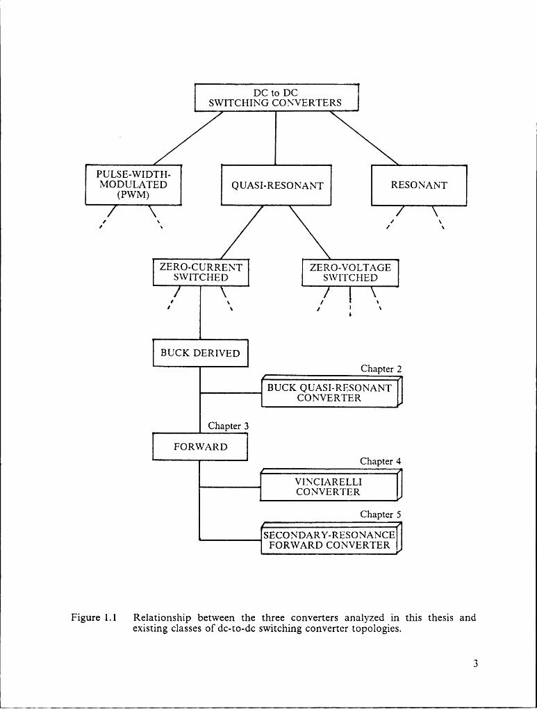
Figure 1.1 shows a classification tree of dc-to-dc switching converter topologies. Themajor categories of dc-to-dc switching converters are: pulse-width·modulated (PWM)converters, quasi-resonant converters, and resonant converters. Currently, PWMconverters are the most common because they are best understood. The resonantconverters, which reduce switching losses and stress compared with PWM converters,have been used in limited applications and usually only for inverters and higher powersystems.
1. INTRODUCTION 2
1 l
DC to DCSWITCHING CONVERTERS
PULSE-WIDTH-MODULATED QUASLRESONANT RESONANT
(PWM)
I x I \I x I \
ZERO-CURRENT ZERO-VOLTAGESWITCHED SWITCHED
I \ / \I \ } l \•
BUCK DERIVEDChapter 2
BUCK OUASI-RESONANTCONVERTER
Chapter 3
FORVVARDChapter 4
VINCIARELLIl CONVERTER
Chapter 5
SECONDARY-RESONANCEFORWARD CONVERTER
Figure 1.1 Relationship between the three converters analyzed in this thesis andexisting classes of dc-to-dc switching converter topologies.
3

Quasi-resonant converters (QRCs) are the newest class of switching converters.
Although some transformer-isolated converters of this type were introduced earlier [5,6],
it has only been recently understood that there exists a large family of converters in thisclass. The term "quasi-resonant" [7], refers to converters which are a hybrid between
PWM converters and resonant converters. Quasi-resonant converters possess the
advantages of simple topologies, like PWM converters; and reduced switching losses, like
resonant converters. In general, a QRC is formed from a PWM converter by replacing
each conventional active switch with a "resonant switch." The resonant switch is
actually a network consisting of an LC resonant tank and a switch (transistor and
diode). Resonant switches can be either zero-voltage-switched or zero-current—switched.
The resonant tank shapes the switch voltage or current (depending on type of resonant
switch), to minimize switching stress andlosses.The
quasi-resonant converters can be divided into two categories, depending on the typeof resonant switch used, as illustrated in Figure l.l. In this thesis, the QRCs analyzed
are of the zero-current·switched type. This means that there is virtually zero current
through the switch when it is turned on and off, and at the switching instants there are
no step-changes in the switch current. Henceforth, in this thesis, all references to
quasi-resonant converters will imply zero-current-switched unless otherwise stated.
Under the category of zero-current-switched converters, for every PWM converter there
exist a number of corresponding quasi-resonant converters. The buck-derived converters
have been chosen for study in this thesis since the PWM versions have relatively simple
dc and small—signal ac characteristics. Buck-derived, quasi~resonant converters includethe buck QRC and forward QRCs of which there are a number of variations.
I. INTRODUCTION 4

[
1.2 Preview of Material Incladed in this Thesis
This thesis discusses the dc steady—state operation and characteristics of the buckquasi-resonant converter (QRC) and two versions of the forward QRC. Circuit analysisand computer simulations are used to study the behavior of these converters. Also,breadboard circuits have been constructed in the laboratory and experimental results arecompared with the theory. The effects of parasitic elements on dc voltage gain andefhciency are presented. To explain these results, the effects of parasitics on thewaveforms within the converters are demonstrated. Design guidelines are given formaximizing converter efliciency. Parasitics also affect component stresses, andexpressions are derived which predict these stresses. The following paragraphssummarize the contents of this thesis.
Section 1.3 describes the circuit simulation program called IGSPICE which is used tosupplement the circuit analysis. IGSPICE provides a convenient way to gain insightinto the complexities of circuit operation when parasitic elements are introduced. Alsoincluded is a description of IGSPICE models for various components within thequasi-resonant converters.
Chapter 2 presents a dc analysis of the buck QRC which is shown in Figure l.2a.Previously, the voltage-conversion ratio for this converter had been determined for thecase where parasitic losses have been neglected [2]. In this analysis, the effects ofequivalent series resistance (ESR) in the resonant inductor and resonant capacitor areincluded. lt is shown that the dc voltage gain can increase with increasing losses forcertain operating conditions. The effects of losses on the resonant tank waveforms are
1. INTRODUCTION 5[[[

I
<=‘> Ii/ ‘°CO DF
•
•rb) co DF CFLo .
>• •(
>••<¤> Co D,.
lLo
Figure 1.2 The buck·derived, zero-current-switched quasi-resonant convertcrsanalyzed in this thesis.a) Quasi-resonant buck converter.b) Vinciarelli converter (reset by parasitics).c) Vinciarelli converter with reset winding. _d) Secondary-resonance forward converter.
6

demonstrated to explain the results of the dc analysis. The exact results of the dc
analysis can only be found by numerical methods or from graphs. To provide more
analytical insight, simple, approximate expressions which predict the dc Voltage gain and
efficiency are derived in Section 2.4. Using these results, design guidelines to maximize
converter efficiency are presented in Section 2.5.
Chapter 3 serves as an introduction to various forward QRC topologies which can resultwhen a transformer is added to the buck QRC. The analyses of these forward
quasi-resonant converters are given in Chapters 4 and 5.
Chapter 4 discusses two implementations of the forward quasi-resonant topology known
as the Vinciarelli converter [5]. Like the PWM forward converter, the quasi-resonant
forward converters must have a means by which the transformer core flux can be reset.
If external circuitry is not added to the Vinciarelli converter the transformer will be reset
due to circuit parasitics. Section 4.1 examines the implementation of the Vinciarelli' converter where the parasitics are used advantageously to reset the transformer core.
This case is represented schematically by Figure 1.2b. The dc characteristics including
parasitic effects for this implementation are presented. An expression is derived to
predict the transistor Voltage stress which is a function of the Values of the parasitic
elements in this type of operation. The other implementation studied is presented inSection 4.2. In this case, external circuitry is added to provide a more controlled
transformer reset in the Vinciarelli converter using a standard technique usually
associated with the PWM forward converter. A diode in series with a tertiary
transformer winding is placed across the input Voltage source as illustrated in Figure
1.2c. A practical converter using this reset mechanism is demonstrated in Section 4.2.2.
1. INTRODUCTION 7

Chapter 5 analyzes a recently introduced forward quasi-resonant topology known as thesecondary-resonance forward converter [ll], shown in Figure 1.2d. Its operation anddc characteristics are different from the other converters of Figure 1.2. An advantageof the secondary-resonance forward converter is that the transformer flux is resetinherently within the converter topology. No external reset circuitry is required, and thereset is not dependent on parasitics. Also, this converter can operate in either full-waveor half-wave mode, whereas the Vinciarelli converter only operates in half-wave mode.When the secondary-resonance forward converter operates in full-wave mode it is muchless sensitive to load variations than is the Vinciarelli converter. Section 5.1 presents thecircuit operation and topological stages. The dc characteristics are derived in Section5.2. Device stresses, which are a function of the dc operating point in this converter, arederived in Section 5.3.
Chapter 6 concludes the thesis with a summary of results and suggestions for furtherstudy.
Appendices A and B contain derivations of the dc characteristics for the convertersanalyzed, the results of which are used throughout the thesis.
1.3 IGSPICE Circuit Simulation Program and Component
Models
Usually parasitics in a physical circuit are undesirable because most circuits exhibit idealcharacteristics only when the components individually behave in an ideal fashion.
1. 11~mzonuc*r10N 8

However, some circuits are designed to take advantage of the existence of certainparasitics. For example, with an isolated PWM converter it is necessary to minimize theparasitic leakage inductance of the transformer, whereas with many isolatedquasi-resonant and resonant converters it has been shown that the leakage inductancecan be used to effectively form all or part of the resonant inductance.
In quasi-resonant converters there are many parasitic elements which can influencecircuit behavior. With the trend toward higher operating frequencies, these parasiticeffects become more pronounced, and at very high frequencies they can even dominatea converter’s response. As more parasitic elements are taken into account in a particularconverter, the circuit topology becomes increasingly complex and the analysis becomesmore involved. As will be shown, parasitic elements can cause additional topologicalstages to be encountered during the switching cycle. Because of the topologicalcomplexity and the inherent nonlinearity of the switching converter, computer
simulation can be used as an effective tool for the study of parasitic effects.
For this thesis IGSPICE is used to simulate the quasi-resonant converters beinginvestigated. IGSPICE, sold by AB Associates in Tampa, Florida, is a digital computer
program that simulates the performance of electronic circuits. For transient(time-domain) analysis it uses a variable time-step iteration technique. The "lG" partof the acronym stands for "interactive graphics." IGSPICE is an advanced version ofSPlCE—2 [12], having the ability to display waveforms resulting from time-domain circuit
simulations. Once a basic circuit has been stored in the computer, parasitic elements canbe added as needed. The effects of a parasitic element can be found by varying its valuefor a number of simulation runs. q
1. INTRODUCTION 9

lt is sometimes difficult to measure certain currents or voltages in a real circuit. Forexample, in a high frequency converter with a physically compact circuit layout it maybe very difficult to monitor magnetizing current in a transformer. With IGSPICE thecircuit can be simulated and any current or voltage may be selected for display. Thesimulation combined with actual lab measurements can provide a thoroughunderstanding of complex circuit behavior. Sometimes there are parasitic element valueswhich are not well known. In these cases the values can be adjusted until a close matchis obtained between the simulated waveforms and those obtained in the laboratory.
A model of a circuit can only be as good as the models for each of the components.Besides having the capability to model pure resistances, inductances, capacitances, andsources, IGSPICE has internal models for various semiconductor devices. The structureof these models is fixed but the user supplies the values for the device parameters. Also,the user may develop specialized models, or make additions to the ones alreadyavailable.
All the circuits investigated in this thesis use a MOSFET as the active switching element.IGSPICE has a MOSFET model [12] which is applicable to any insulated-gate FET.The model was modified for use as a HEXFET (International Rectifier trademark for ‘
their power MOSFETS) and is shown in Figure 1.3. The values of the parameters usedin the equations for the MOSFET model were found by using a procedure [13] whichenables one to determine model parameters from the manufacturer’s device data sheet.
IGSPICE has an intemal model for diodes shown in Figure 1.4. This model includes theeffects of two charge-storage mechanisms in a diode. Charge storage in the junctiondepletion region is modeled by CJ, and charge storage due to injected minoiity carriersis modeled by CD.
1. 1NTRODuc'1‘10N 10

I1
D
LD
E RD E: CoD .
RG * vé'° - . IG. v}, ID CDS A pgp:: cos :
E * Vb-R5L.......-----.-.----.......{
LS
wams:0, v'GS s VT AND VOD s vr
(CUTOFF)
/0 ¤ Kp V'DS[(\/'GS · VT) V'Gs 2 VT AND V'GD 2 VT(OHMIC)
I/TFH + M/’D$I . VG, 2 v, Auo v·„ s v,(PINCH OFF)
gps • .[L.._/ V'os1+ PB
Figure 1.3
IGSPICE MOSFET model, modified for cvHEXFET application. .
CJ"
ID RS
+ V) ··Vo
ID = IS
"Figure1.4 CD ” „ VT ° nw
IGSPICE diode model.CJ, - &)„„
PB
ll

I
I
PRIMARY PRIMARY SECONDARY SECONDARYRENSTANCE INDUCTANCE INDUCTANCE RESISTANCE
RI 1.n *-7- R2
EFFECTIVE EFFECTIVEPRIMARY SECONDARY _SHUNT _n SHUNT
CJ CAPACITANCE LH RH IDEAL CAPACITANCE C-1MAGNETIZING 1·g1·A;_INDUCTANCE ggg; _
LOSS
Figure 1.5 High-frequency power transformer model.
3) b)*-°° EQUIVALENT
+° + +- I«.oA1• +“U’ C·¤¤ R U;_ Lo/tb _ _
Ä: _ C:Ts1'U"U’
U1 I*1HO x V
TS1
TS TS1 .
VOUT='T' Vdt=""" Ä.dt=‘VCTS C0 0 0
Figure 1.6 Infinite filter-inductance assumption. This reduces computer simulationtime by attaining steady state "irnmediately”.
12

A general model for a high-frequency power transformer is shown in Figure 1.5. Thismodel was implemented in IGSPICE using the discrete components shown.
In many cases the filter-inductor current of a quasi—resonant converter can be assumedconstant. When this assumption is valid, the output filter and load can be modeled byan equivalent circuit as shown in Figure 1.6. This reduces the amount of computersimulation time required for the circuit to reach steady state. The filter inductor andcapacitor of Figure 1.6a must be given correct initial conditions (not always accuratelyknown beforehand); otherwise, the simulation will require many switching cycles toreach steady state. The circuit in Figure 1.6b presents a constant current sink to theresonant tank. The output voltage is found after one switching cycle and is equal to thevalue of vc at time Ts (the switching period). The resistor in Figure 1.6b is very largein value, but must be present for IGSPICE to work properly.
1.4 Termirwlogy
Table 1.1 defines the symbols used in this work.
In this thesis the "secondary-resonance forward converter" refers to the forwardconverter with secondary·side resonance, shown in Figure 1.2d, which was introduced inReference [11].
There are various implementations of the Vinciarelli converter depending on the methodby which the transformer's core is reset. ln this thesis the "Vinciarel1i converter" refersto the forward converter switching at zero current, shown in Figure 1.2b, patented in
1. INTRODUCTION 13

[
Reference [5]. The "Vinciarelli converter with reset winding" refers to the convertershown in Figure l.2c. None of the implementations of the Vinciarelli converterdiscussed in this thesis necessarily represent the actual implementation of the Vinciarelliconverter manufactured by the Vicor Corporation. Because of the differences inimplementation, the converter manufactured by Vicor may have some differentcharacteristics than those presented in this work.
Although the Vinciarelli converter employs the secondary-side resonance techniquepresented in Reference [1 1], the terminology defined in the previous two paragraphs willbe used in this thesis to avoid confusion between the converters studied.
1. INTRODUCTION 14

Table 1.1 Definition of symbols used in this thesis.
CDS MOSFET drain-source capacitanceCF Filter capacitorCFWD Forward-diode junction capacitanceCO Resonant capacitorDA Antiparallel diodeDD Blocking diodeDDD MOSFET body·drain diodeDF, DFW Freewheeling diodeDFWD Forward diodeDRESET Reset diodeDS Series diodefD, FD Resonant frequency
= 1/(2¤\/LOCO )fjg, FS Switching frequencyfS /fD Normalized switching frequencyIC Resonant-capacitor currentIC ,,,,5. RMS resonant-capacitor currentil, Resonant-inductor currentiL ,,m. RMS resonant·inductor currentIM DC magnetizing current in transformer (referred to secondary)IMN Normalized dc magnetizing current
ID DC output currentICN Normalized dc output current
IQ peak Peak current through transistorLF Filter inductorLM Transformer magnetizing inductance (referred to primary)LO Resonant inductorL'O Resonant inductance referred to the transformer secondaryM DC voltage gain
NF Number of turns on transformer primaryNS Number of tums on transformer secondaryPIN DC input powerPLDSS DC power lost in converterPDUT DC output powerQ Normalized load resistance
= R/ZDQRC Quasi-resonant converter
I5

Table 1.1 (Continued)
R Load resistanceR/ZO Normalized load resistancefz Temporary variable (see Figures B.2 and B.6, and Equation (5-4))RC Resonant—capacitor ESRRL Resonant·inductor ESRz TimeATM MOSFET gate "on"-time marginTO Resonant period
= 1/FOZQ MOSFET gate "on" timeVC Resonant-capacitor VoltageVCON Normalized initial resonant-capacitor Voltage
(see Figures B.2 and B.6)VD; MOSFET drain-source VoltageVD;pN Normalized peak drain-source Voltage on the MOSFET
= VPEAK/ VsVL Resonant inductor VoltageVM Transformer primary VoltageVN Magnitude of negative peak Voltage on transfoxmer primaryVO DC output VoltageVPEAK Peak drain-source Voltage on the MOSFETV; DC input VoltageV'; DC Input Voltage referred to the transformer secondaryX Normalized switching frequency
= Fs/FoZ0 Characteristic impedance
= „/YZF?QL- Damping factor related to resonant capacitor ESR= Rc / ( 2 Z0) ·QL Damping factor related to resonant inductor ESR
= RL / ( 2 ZO)11 Converter efficiencync Converter efiiciency due only to resonant-capacitor ESR11 L Converter efliciency due only to resonant—inductor ESR9 Phase angle
= cutco, 600 Resonant frequency in radians per second
= 1/\/LococoR Reset frequency in radians per second
= 1/«/(LM + L0)C0s
16

2.1 Review of Ideal Circuit Operation and DC
Characteristics
2.1.1 Ideal Circuit Operation
Figure 2.1 shows a circuit diagram and typical waveforms of the buck QRC(quasi·resonant converter). This particular implementation uses thezero-current-switched L-type switch in half-wave mode [1]. Table 1.1 includesterminology describing the circuit elements. The diode, DS, in series with the resonantinductor, LO, allows current flow only in one direction. This is known as half-wavemode. In full-wave mode, to be discussed later, the resonant-inductor current is allowedto flow in both directions by the addition of an antiparallel diode,
2. THE QuAs1-Rnsommr sucx cowvmzrmz 17

DS LO LF ,L’0Vs ‘“ Co DF DF F
- ÄLO RESONANT INDUCTOR CURRENT
To{0
2VS IT/E30 RESONANT CAPACITOR VOLTAGE
O .ToT1 T2 T3 T4VS [VDS FET DRAIN—SOURCE VOLTAGE
ToT1 T2 Ta T4
Figure 2.1 Buck quasi-resonant converter (half-wave mode) and typical waveforms.
18

In normal operation the buck QRC cycles through four topological stages for eachswitching cycle. The stage changes at times indicated by TO through T4. Circuitoperation in half-wave mode is described below with the time interval indicated for eachstage. (See waveforms in Figure 2.1.) This description assumes that the circuitcomponents are ideal and the filter inductor, LF, is much larger than the resonantinductor, LO, so the filter-inductor current can be considered constant.
Time Interval [TO — T1]
At time TO, the transistor is turned on externally (by the control circuitry). Immediatelybefore TO, the resonant—inductor current and resonant-capacitor voltage are both zero
[
and the freewheeling diode is conducting the filter-inductor current. After TO, theresonant-inductor current charges linearly with time until T1. At T1, theresonant-inductor current equals the filter-inductor current and the freewheeling diodeturns off
Time Interval [Tl — T2]
LO and CO resonate during this stage. Ideally, the resonant-capacitor voltage reaches apeak equal to twice the input voltage and then begins to decrease. The stage ends atT2 when the resonant-inductor current decreases to zero and the series diodecomrnutates off
Time Interval [T2 — T3]
The filter-inductor current then discharges the resonant capacitor linearly. During thistime the resonant-inductor current remains at zero. Note that the transistor must beturned off after T2 but before the resonant-capacitor voltage decreases to less than theinput voltage to prevent the resonant—inductor current from flowing again until the nextswitching cycle. This stage ends at T3 when the resonant-capacitor voltage becomes zeroand the freewheeling diode tums on.
2. THE QUASI-RESONANT BUCK CONVERTER 19

Time Interval [T3 — T4]
The converter remains idle during this stage with the resonant-inductor current andresonant-capacitor voltage at zero. The freewheeling diode conducts the filter-inductorcurrent. This stage continues until the transistor is turned on again by the controlcircuitry.
To obtain the full-wave mode implementation of the buck QRC from the half-wavemode, an antiparallel diode, DA, is placed across the transistor and series diode, as
shown in Figure 2.2. This allows the resonant-inductor current to reverse direction, as
illustrated in the corresponding waveforms of Figure 2.2. The converter cycles through
the same stages as described for the half-wave mode, except the resonant stage does notend until the resonant-inductor current becomes negative and then returns to zero. Inthe full-wave mode, the transistor must be turned off during the negative
resonant-inductor current interval. It is possible to operate in full—wave mode by using
a MOSFET without external diodes DA and DS since the MOSFET includes an internaldrain-source antiparallel diode. This will not work well at high frequencies, however,
because the internal MOSFET diode has a relatively slow reverse recovery.
From the description of the buck QRC operation, it should be observed that the circuit
operation is insensitive to the turn-0fT time of the MOSFET as long as turn-off occurssoon after diode DS (in half-wave mode) or DA (in full-wave mode) naturally
commutates off This implies that for a particular buck QRC, the MOSFET is driven
with constant on—time and the switching frequency is varied to achieve control of theoutput voltage.
2. THE QUASI-RESONANT Buck CONVERTER 20

D
P08 Lo LF llovs ‘“ co 0,: CF R
ÄLO RESONANT INDUCTOR CURRENT
IE F2T0T1 Ts T4
2VS li/CO RESONANT CAPACITOR VOLTAGE
OT T T T T1/ FET DRAIN-SOURCE VOLTAGEDSVs
Figure 2.2 Buck quasi-resonant converter (f”u1l—wave mode) and typical wavcforms.
21

2.1.2 DC Voltage Gain for the Lossless Buck QRC
The dc voltage gain of the buck QRC has been analyzed for the lossless case inReference [2]. The results are repeated here for comparison with the analysis presentedin Section 2.2, which includes the effects of losses in the converter. An assumption madein both cases is that the filter inductance is large enough that the filter-inductor currentcan be considered constant. This is usually a good assumption. When the filter-inductorcurrent variation becomes large, new modes of operation can occur which are discussedin Reference [14]. The results of the dc voltage gain analysis are plotted in terms ofnormalized parameters. Therefore, the curves are applicable to any buck QRC of thetopologies shown in Figures 2.1 and 2.2 regardless of the actual component values. Thenormalized parameters used in this thesis are given with their definitions in Table 1.1.
Figure 2.3a shows the ideal dc voltage-conversion ratio versus normalized switchingfrequency for half-wave mode. The individual curves on each plot represent differentvalues of the normalized load resistance. Figure 2.4a shows the same parameters plottedfor the full-wave mode. The dc voltage-conversion ratio in full-wave mode is almostindependent of load because excess resonant tank energy is returned to the input voltagesource through the antiparallel diode, DA.
2. THE QUASI-RESONANT BUCK CONVERTER 22

(¤> IIEEIEIIHII (¤> IIIIIIIIIIIIIIIIEI E IIIIIII?IMIIIIIIII 6 IIIIIIVI I_.§· IIVIHIHIIIII 6;IIIIIIAaIII6 IIMIHHIIII 6 IIIIIV IIIFl IIIIHBV II Ei EIIIIIIIIIg. WMEHIIIIII S. I=aIIIIII;. I%lIIIIIII IIV IIIIIIMIIIIIIIIIU.0 0 0.2 0.0 0.0 1 0
(b> IIIIIIIIII (0) IIIIIIIIIIC IIIIIIIIII IIIIIIIEZI6 IIIIIIIIII Sg IIIIIIIAI§ IIIIIIIIII 6 IIIIIWMIII6 IIIIII! I 6 IIIIIWIIIIä IIAIAIIIIIIII Ci IIIIÄIIIIIg. WIIVIIIIIII g. III7
4I‘%'lllII ulllll<¢> IIIIIIIIII (¤>· IIIIIIIIII
E IFIHIBIIZHI E IIIIIIIIII6 IIIIIIIIII 6 IIIIIII%IIlßllll mm III6 IIIIIIHIIII 6 IIII!%IIIIä IHHIQIIIIII ä IIII%IIIII· ; IMIQEIIIIII g. lII„%IIIIII
E MZHIIIIIII ;. g I%IIIIIII%HIIIIIIII %IIIIIIII.’ ! C C .7;/ lo (NONDIÜÜZDÖ Switching Fr•qu•ncy)1.· 7; / fo (girmaiizw Switching Fr•qu•ncy) ·
Figure 2.3 Figure 2.4DC voltage gain of the half-wave DC voltage gain of the full-wave buckbuck QRC. R/ZO is the normalized QRC. R/ZO is the normalized loadload resistance. resistance.a) Lossless case. a) Lossless case.b) With resonant inductor ESR b) With resonant inductor ESR(CL = 9-1)- _ (CL = 0-05)- _c) With resoriant capac1tor ESR c) With resonant capacxtor ESR(gc = 0.1). (gc = 0.05).
23

2.2 DC Voltage Gain and Eßiciency for the Buck QRCWith Losses
This section describes the results of a de analysis, including the effects of losses, for thebuck QRC. The analysis was performed by solving the state equations for eachtopological stage and then matching boundary conditions between the stages. AppendixA contains the details of the analysis, with a complete description of the procedure. Theresults were computed numerically and then plotted as functions of normalizedparameters. It is assumed, as in the lossless case, that the filter-inductor current isconstant. The resistive losses in the circuit are lumped as resonant-inductor BSR andresonant-capacitor BSR and are characterized by their equivalent damping factors,QL and QC, respectively, to normalize these parameters. The definitions of the dampingfactors are given in Table 1.1.
Graphs b and c of Figures 2.3 and 2.4 show how the dc voltage gain is modified whenlosses are introduced. The parasitic damping factors are constant for each plot whilenormalized switching frequency is varied for comparison to the lossless case (Figures2.3a and 2.4a). The effects of losses are better understood when the damping factors arevaried as a parameter. The results of this are discussed in the following paragraphs.
Half-Wave Mode: Figures 2.5a and 2.5b illustrate the effect of increasingresonant-inductor BSR on the voltage gain and efficiency for the half—wave mode. Thenormalized switching frequency was chosen to be 0.3 for these plots. Figures 2.5c and2.5d show the effect of increasing the resonant—capacitor BSR. Resonant-inductor BSRand resonant-capacitor BSR have very similar effects. The voltage gain and efficiency
2. THE QUAS1-RESONANT Bucx CONVERTER 24

8IIIII CV II V NIIIIg \IIIII XIIII·;·° Ä ät: ‘IIIgtI _g‘III=ä%.® 0.l0 0.E 0.§ 0.40 0.50 .¤) 0.l0 0.20 0.ä 0.40 0.50CL CL
8
IIIII Qd „IIIII V LIIIIIIIII l¤IIIIII? IÄII
Q
_
§ ·IIIII älücb.® 0.I0 0.20 0.§ 0.40 0.50 .® 0.lO 0.20 0.3) 0.0 0.50Cc Cc
Figure 2.5 Effect of ESR on the half-wave buck QRC at FS/ FO = 0.3.a) DC Voltage gain versus normalized resonant inductor ESR.b) Efficiency versus normalized resonant inductor ESR.c) DC Voltage gain versus normalized resonant capacitor ESR.d) Efficiency versus normalized resonant capacitor ESR.
25

QEIIIIII t3IIl W MNIIIIIQ 7 llY.IEllII .M§IIII'$’ E.%IIIII ämhägll
3 h 3 . ‘ 1 =.lIEllI . Illqlw 0.ß 0.10 0.15 0.20 0.25 0.§ 0.05 0.10 0.15 0.20 0.25 0.w
C1. C1.
Q.IIlIlä .0 7 -<·=> r <d>gII!4lI .&!lIIIEIEAIII ÄMBEIIIgs Ih$WW"ii *NIÜ"ä° i" hu.IIllII .Nll¤-¤.IIIIII .MÜIIII%.® 0.G 0.10 0.15 0.E 0.25 0.ä 0.10 0.15 0.20 0.25 0.§Cc Cc
Figure 2.6 Effect of ESR on the full-wave buck QRC at FS/ FO = 0.5.a) DC Voltage gain versus normalized resonant inductor ESR.b) Efficiency versus normalized resonant inductor ESR.c) DC Voltage gain versus normalized resonant capacitor ESR.d) Efficiency versus normalized resonant capacitor ES R.The Voltage gain can increase with ESR if the converter is lightly loaded.
26

both decrease when BSR is increased, as might be expected with the introduction of ilosses.
Full-Wave Mode: Figures 2.6a and 2.6b illustrate the effect of increasing theresonant-inductor BSR on the dc voltage gain and efliciency for full-wave mode. Theeffect of increasing the resonant-capacitor BSR is shown in Figures 2.6c and 2.6d. Theseresults, for full-wave mode, are plotted with the normalized switching frequency equal
· to 0.5. In this case the dc voltage gain increases or decreases with increasing BSRdepending on the value of the normalized load resistance. For light loads (highernormalized load resistance), the dc voltage gain tends to increase with increasing losses.It may, at first, seem unusual that the dc voltage gain can increase as the losses in theconverter are increased. This will be explained in Section 2.3. The efficiency, whichalways decreases with increasing losses, is much more sensitive to load variations infull-wave mode than in half-wave mode.
As these plots (Figures 2.3 through 2.6) are examined, it will be observed that theindividual curves representing various load resistances terminate at different values ofthe x-axis parameter. A particular curve ends when the converter no longer operates inthe desired mode. For a sufficiently high value of the x-axis parameter, the desiredoperation, described in Section 2.l.l, will not be achieved. There are two possibleconditions which will cause a different mode to be encountered. One condition is wherethe resonant—inductor current does not naturally return to zero. In this condition, whenthe switch is turned off, the current is forced to zero, and the zero—current switchingproperty of the converter is lost. (Zero-current switching implies that the transistorcurrent is zero at turn-on and turn-off and there is no abrupt change in transistor currentat the switching instants.) The other condition occurs when the resonant-capacitor
2. THE QUASI-RESGNANT BUCK CONVERTER 27

voltage does not return to zero before the switch is turned on. This causes the converterto operate in a different mode. The analysis of other operating modes is not coveredhere, but can be found in Reference [7], for the lossless case.
2.3 Eßect of Losses on the Back QRC Resonant TankWaveforms
To illustrate why the dc voltage gain can increase with added ESR in full-wave mode,the effects of losses on the resonant tank waveforms are shown. Figures 2.7a and 2.7bshow the waveforms for a lightly-loaded buck QRC in full-wave mode with no losses.The waveforms for the same converter, except having added resonant-inductor ESR, areshown in Figures 2.7c and 2.7d. When losses are introduced, energy is lost throughoutthe resonant stage causing a smaller portion of the total tank energy to be returned tothe input voltage source. This can be observed in Figure 2.7c where theresonant-inductor current becomes a sinusoid with an exponentially decaying envelope.In this figure, the ratio of negative amp-seconds (proportional to energy returned to thesource) to positive amp-seconds (proportional to energy taken from the source) issmaller than for the lossless case in Figure 2.7a.
Modification of the resonant-inductor current, due to losses, affects theresonant-capacitor voltage as follows. Although the resonant-capacitor’s peak voltagebecomes lower than the ideal (twice the input voltage), the capacitor takes longer todischarge because less of its energy was returned to the source. It will be noted that thearea under the resonant·capacitor voltage waveform is greater in the case with losses.
2. THE QUASI-RESONANT BUCK CONVERTER 28

a) RESONANTINOUCTOR CURRENT b) RESONANT CAPACITOR VOLTAGE(LOSSLESS CASE) (LOSSLESS CASE)
c) RESONANT INDUCTOR CURRENT d) RESONANT CAPACITOR VOLTAGE(WITH LOSSES) (WITH LOSSES)
Figure 2.7 erregt of parasitic losses on resonant tank waveforrns of the f‘u11—wave buckQRC.
a) RESOHANT INDUCTOR CURRENT b) RESONANT CAPACITOR VOLTAGE(LOSSLESS CASE) (LOSSLESS CASE)
c) RESONANTINWCTGR CURRENT 6) Rssorumr cArAcn*oR votmcs(WITH LOSSES) (WITH LOSSES)
Figure 2.8 EtTect of parasitic losses on resonant tank waveforms of the half-wavebuck QRC.
29

ISince the output voltage is the average of the resonant-capacitor voltage, and theswitching time remains constant, the output voltage increases with the addition oflosses.
The efTect of losses on the waveforms for half-wave mode is now examined. Figures 2.8aand 2.8b show waveforms for a half~wave buck QRC without losses. Whenresonant-inductor ESR is added, the waveforms appear as in Figures 2.8c and 2.8d. Thegeneral shape of the waveforms remain the same but the amplitudes decrease with lossessince energy is never returned to the source. Therefore, the area under theresonant-capacitor voltage waveform decreases when losses are introduced. Thisillustrates why the output voltage always decreases with increasing losses for the buckQRC in half-wave mode.
2.4 Simple, Approximate Expressions to Predict DC
Voltage Gain and Eßiciency
In Section 2.2, exact results were given for the dc voltage gain and efficiency of thequasi·resonant buck converter when parasitic losses are included. The exact results canonly be computed numerically because the analytical solution is in the form of implicitequations (see Appendix A). lt is desirable to obtain explicit expressions for the dcvoltage gain and etliciency; however, this requires that some approximations be made.In this section, these approximate expressions are derived. It will be demonstrated thatfor most operating conditions, the approximate results match the exact results quiteclosely. The results of this section are then used in the next section to provide the circuitdesigner with a strategy to maximize converter efliciency.
2. THE QUASI-RESONANT ßucx coNvERTER so

n 1lTo simplify the expressions in this section, the following symbols are used (see also Table1.1):
M = VO/VS , DC Voltage GainX = FS/FO , Normalized Switching Frequency
Q = R/ZO , Nonnalized Load Resistance
Before proceeding with the derivations of approximate expressions to predict dc voltagegain and efficiency, it is necessary to digress briefly to show that Q 2 M for normaloperation of the buck QRC (both in full-wave and half-wave mode). This result will beused later in this section and in Section 2.5.
During the resonant stage (interval [T) — T2], as described in Section 2.1.1) theresonant-inductor current is given by:
12 — /0 + — Sm l<¤(¢ · Ti)l (2 — 1)Z0
To achieve Zero-Current switching the resonant-inductor current must naturally returnto zero. This can only happen ii
V1 S J 2 — 20 ZO ( )
Manipulating this constraint gives,
I Z Z(ZE;).-[ON-.iM-..s>lK’.-M. (2-3)VS VO R Q
Therefore, it has been shown that Q 2 M, thus concluding this digression.
2. THE QUASI-RESONANT Bucx coNvERTER 31

The approximate expressions for dc voltage gain and efficiency are derived separately forfull-wave and half-wave modes. The derivations will now be given.
2.4.1 Full-Wave Mode
2.4.1.1 Voltage Gain: In full-wave mode the ideal dc voltage gain is approximately equalto the normalized switching frequency [2],
FM;x=—i 0-o. FO
This result will be used in deriving the approximate efficiency with losses, next.
2.4.1.2 Efficiency: Resistive losses in the circuit are assumed to be lumped asresonant—inductor ESR and resonant—capacitor ESR. The converter efficiency due toeach of these losses is computed separately to gain insight into the effects of each. Theresulting efficiency due to both losses is then be found by superposition of the individual_losses, which is a valid approximation.
It is assumed in this analysis, that the addition of parasitic resistance is small enoughthat it does not cause the resonant-inductor current or resonant-capacitor currentwaveforms to change. This is a valid assumption for practical circuits where theefficiency must be maximized. The efficiency is found by first determining the loss,which is equal to the parasitic resistance multiplied by the square of the rms currentthrough the parasitic resistance. This approach is similar to that used in the analysisof efficiency for the series and parallel resonant converters given in Reference [15]. Theefliciency is given by:
2. THE QUAS1-RESONANT BUCK CONVERTER 32

P PIN our 1.0ss 1 + Loss
Pour
2.4.1.2.1 Efficiency Due to Resonant-Inductor ESR Only: The loss in theresonant-inductor ESR, and the output power are given by:
Ptoss = lim.- R1. (2 ” 6)
Pour = VÖ/R (2 ‘ 7)
To find a simple expression for the rms current through the resonant inductor, it isassumed that the resonant-inductor current is exactly one cycle of a sinusoid during thetime when the switch is conducting. This is shown in Figure 2.9. When thisapproximation is made, the mean-square value of the resonant-inductor current is:
F /F 2 . (2-8)
where,
VZo
Substituting Equation (2-9) into (2-8), performing the integration, and using M = Xgives, ·
2 ViPLOSS = M IO RL (2 — 10)
Dividing Equation (2-10) by (2-7), and writing the result in terms of normalizedparameters results in,
2. THE QUAS1-REs0NANT Bucx CONVERTER 33

RESONANT INDUCTOR CURRENT
{ VS/ZO,00
1 { "’{ g cot
21:21:-—-1—•1 RESONANT CAPACITOR CURRENT
FS/FO Q_ VS/ZO ‘
0 Q ...t-. Q —)•{ ; (Dt
Z<-———21:Figure
2.9 Approximate waveforms for the full-wave buck QRC.
RESONANT INDUCTOR CURRENT
,0.=.....1..--O{ : a
_>
: E S mt:*-**-*2 ;é
··ÄTE— Q RESONANT CAPACITOR CURRENT
'•
0 Q ..!.. ‘- IO E ä Q (Dt
· S N 2Q ·
Figure 2.10 Approximate waveforms for the haltlwave buck QRC.
34

PLOSS 21/I +QL= L L Q (2 — 11)Pour Q M L
Substituting this into the extreme-right side of Equation (2-5) gives the efficiency infull-wave mode due to ESR in the resonant inductor which is,
rr. =L (2 — 12)1 .. „. 2 CLQ M
2.4.1.2.2 Efficiency Due to Resonant-Capacitor ESR Only: The method used above todetermine the eflficiency due to the resonant-inductor ESR is used here. The currentthrough the resonant capacitor is assumed to be a complete cycle of a sinusoid when theswitch is conducting, as shown in Figure 2.9. With this approximation, the mean-squarecurrent through the resonant capacitor is,
F /F 2 .rgm = .16 (2 — 13)
where,
VS •i = —·——s1n 9 (2 — 14)
The power loss in the resonant-capacitor ESR is:
1 M VéPLOSS = ICrms Rc = —?Rc (2 ‘ 15)
Dividing Equation (2-15) by (2-7) and substituting into (2-5) gives the desired result.The efliciency in full-wave mode due to ESR in the resonant capacitor is,
2. THE QUASI-RESONANT ßucx CONVERTER 35

nc = ——¥ (2 — 16)1 + Ä;
Figure 2.11a shows efficiency versus normalized resonant-inductor BSR and Figure2.1lb shows efficiency versus normalized resonant-capacitor BSR. In these figures, theexact analysis (of Section 2.2) is shown as a solid line, and the "dotted" lines are a resultof the approximate analysis above. These graphs are plotted for a value of normalizedswitching frequency equal to 0.5. The agreement between approximate and exactanalysis is quite good for reasonable values of BSR. The effects of resonant-inductorBSR and resonant-capacitor BSR can be combined into one expression by simply addingthe "1oss" terms from Bquations (2-12) and (2-16). The result gives the overall efficiencydue to resistive losses in the buck quasi-resonant converter in full-wave mode:
n = -——-#—-— (2 — 17)1+ 1%+-15711-+w3·1«
2.4.2 Half-Wave Mode
2.4.2.1 DC Voltage Gain: For the half-wave case the approximation for voltage gain is
not quite as simple as for full-wave mode. The dc voltage gain, M, in the ideal case hasbeen derived in Reference [2]. The result is the implicit equation:
(2-18)
2. THE QUASI-RESONANT ßucx CONVERTER 36

O8
i
‘A A A
+ + 0:2+ +
X 0:5
O Ü=lÜLJOÜÖÜBELu X
ci , ·Q- 4 Il1*% X.Cb.00 0.10 0.20 0.30 0.40 0.20 QL¤lO“8"
MYb) C; ~“
+ A Ü:]„„
\
·
+ + + + + O=2j L X 6-6ZLL] O Ü=lÜ
UOÜBÜBE· 0:20üca Y +6 Q. Ö 6
II — IlCb.00 0.10 0.20 0.30 I 0.40 0.50 CCxs lÜ°
Figure 2.11 Comparison of“ exact (solid lines) versus approximate (points) analysis ofthe full-wave buck QRC, for:a) Efficiency versus normalized resonant inductor ESR.b) Efficiency versus normalized resonant capacitor ESR.
E 37

Since Q 2 M, as shown by Equation (2-3), the arcsin and square-root terms can beapproximated. The expression then becomes [16],
gl. JL JL .9. .9. (219)
This makes it possible to solve explicitly for M. The result is:
g_ + gi + 4QX _ sxiM = 2 4 Ti ri 2 — 202 _ 3X ( )
27tQ
If desired, the above expression can be simplified further. Q is always greater than X,which leads to the approximation [16],
... L /% -M 4 + E (2 21)
These approximate results are plotted along with the exact analysis for comparison inFigure 2.12. The solid lines are the results of the exact analysis. The "triang1e" and"p1us" symbols indicate values of the approximations using Equations (2-20) and (2-21),respectively.
2.4.2.2 Efficiency
2.4.2.2.1 Eßiciency Due to Resonant Inductor ESR Only: The resonant-inductor currentis assumed to be exactly a half cycle of a sinusoid during the time when the switchconducts. This is shown in Figure 2.10. The mean-square current through the resonantinductor can then be approximated by:
2. THE QUAS1-RESONANT BUCK CONVERTER 38

EIC)9Ä Ä.1 — 2I ‘
+3 1 Ä 6. ‘ " ^+
O I ‘IF! i.6O_>~q3¤
+> . ‘ -
OCZ
Cb.00 0.20 0.40 0.60 0.80 1.00
SOLID LINES = EXACT SOLUTIONA = APPROXIMATION USING EOUATION (2-20)
+ = SIMPLE APPROX. USING EOUATION (2-21)
Figure 2.12 DC voltage gain for the halflwave buck QRC; comparison of exact versusapproximate analysis.
39

F FIärms = (12 49 (2 * 22)
where,
ViL=IO+?‘i-sin9 (2-23)0
Solving the integration of Equation (2-22) gives:
2 — X 2 2/YIOVO _ILrms"7IO++ (2 24)
Next, the ratio of power loss to power output is:
PLOSS Iärm RL= '*+·"ourVO/R
Substituting Equation (2-24) into (2-25) and writing in terms of normalized parametersgives:
P;·@.=X|:£(;+gC.l;.+£] (2-26)· Pour Q 2M2 M4
Using Equations (2-5) and (2-26), the efliciency in half-wave mode due toresonant-inductor ESR is,
""=—_T—l<§——T— “‘ 27)
In this equation, M can be obtained from the exact analysis of Section 2.2 or from theapproximate analysis above.
2. THE QUASLRESONANT BUCK CONVERTER 40

2.4.2.2.2 Eßiciency Due to Resonant Capacitor ESR Only: In half-wave mode the Ä
resonant-capacitor current is approximately as shown in Figure 2.10. The mean-square Ä
current in the resonant capacitoris,F
2 _ F5/FO 11 Vé . 2 Fg/FO 2Q/M 2S1!} +
(2*Performingthe integration, then using Equation (2-7) and PLOSS = [gms RC, andwriting in terms of normalized parameters gives,
P X...LQ.€-E.;-..§.Q|il+Ä] (2-29)POUT TC
Therefore, the efficiency in half-wave mode due to resonant-capacitor ESR is,
nc = -—-ll--- <2 — sm1 „. Ä. [L ., 2];M 2M TI C
In the above equation, M can be found from the exact analysis of Section 2.2 or from
the approximate analysis in this section.
Figure 2.13a shows efliciency versus resonant-inductor ESR. The exact analysis (solid
curves) is compared with the approximate analysis. Figure 2.13b shows similar results
for resonant-capacitor ESR. ln both figures, the approximate analysis uses the value
of M calculated from Equation (2-20). These graphs are plotted for a value ofnormalized switching frequency equal to 0.3.
The "loss" terms of Equations (2-27) and (2-30) are now combined to determine theoverall etliciency of the buck QRC in half-wave mode due to resistive losses:
2. THE QUAS1-RESONANT Buck CONVERTER 41

O9\\_ A 0:0 .6\\
O .. ‘‘
Ü=56§I-0· .mq § _ ~
C)
°0.00 0.02 0.04 0.06 0.06 0.10 QLOC!
‘\ A @=Ü . 536)C; + @:1
X @:20
@:52M3C)
°0.00 0.02 0.04 0.06 0.08 0.10 Cc
Figure 2.13 Comparison of exact (solid lines) versus approximate (points) analysis of 1the halllwave buck QRC, for: Qa) Bfliciency versus normalized resonant inductor BSR. ,b) Etliciency versus normalized resonant capacitor ES R. ·
42 Q1Il

(n= (2 — 31)
Q Zjwz 1)/[rt
2.5 Design Guidelines to Maximize Converter Eßiciency
Using the approximate results for efficiency obtained in the previous section, designguidelines will be given for maximizing converter efliciency. The goal is to find the Qwhich maximizes efliciency for a fixed M. The value of M relates to the application(voltage gain required) and Q relates to the design of the resonant tank components.The maximization of efficiency will be investigated separately for full-wave andhalf-wave modes. Then, the results will be combined at the end of this section.
Full-Wave Mode: Equation (2-17) gives the efliciency due to resonant-inductor andresonant-capacitor ESR in full-wave mode. To maximize the efficiency, it is necessaryto minimize the normalized loss:
MINIMIZE:
QLwhere,
- RL _ ß _ Rc = Rc _ÖL ZZO ZR Q md Cc 220 2R Q (2 32)
To find the optimum Q for any given application, M, R, RC, and RL are held constant.1Therefore, the minimizationbecomes:2.
THE QUASI-RESONANT BUCK CONVERTER43_

2MINIMIZE: %(RL + RC)
The solution to this minimization is to make Q as small as possible, but, as stated at thebeginning of” Section 2.4, it is necessary that Q 2 M . Therefore, to maximize theefficiency:
QWPTIMUM) = M (FULL-WAVE MODE) (2 — 33)
Half-Wave Mode: Equation (2-31) gives the efiiciency in half-wave mode due toresonant·inductor and resonant-capacitor ESR. To maximize the efficiency:
X X 2MINIMIZE; .2-. + + (2 - 34)QTo
minimize the above expression while maintaining M constant, requires finding X asa function of M and Q. This can be done by solving for X in the simplified equation forM given in Equation (2-21). The result is:
= Q _ M4 _X (2 35)
Equation (2-34) can then be minimized by first making substitutions using (2-32) and(2-35). Then, in Equation (2-34), the partial derivative with respect to Q is taken, andthe resulting expression is set equal to zero. The next step is to solve for the value ofQ. In this case, the resulting value of Q depends on the ratio RL/RC . However,regardless of the value of this ratio, the result always indicates that Q should be smallerthan M. But, since it is necessary that Q 2 M,
QMPTIMUM) = M (HALF-WAVE MODE) (2 — 36)
2. THE QUASI-RESONANT BUCK CONVERTER 44

I
Using the results obtained in this section, the values of the resonant inductance andresonant capacitance are now selected to maximize converter efliciency. The resonanttank components, LO and CO, can be expressed as:
Z0 1L = l , C = — 2 — 37O (00 O (00 ZO ( )
The resonant tank components, therefore, are completely determined knowing theresonant frequency, mo (in radians per second), and the characteristic impedance, ZO.The resonant frequency is usually chosen to be as high as possible. Some factors whichlimit the resonant frequency are: transistor switching speed, transistor drive speed, andpower loss due to discharge of the switch capacitance at turn-on. Once the resonantfrequency is selected, it is necessary to determine the characteristic impedance of theresonant tank. The characteristic impedance can be expressed as the actual loadresistance divided by the normalized load resistance. That is,
- Ä _l Z0 Q (2 38)
Equations (2-3), (2-33), and (2-36) show that to maximize the efliciency of the converter,whether in full-wave or half-wave mode, Q should be made as small as possible whileQ 2 M . Manipulating this constraint, using Equation (2-38), ·
Rmin _Qmm = Mmax —> —··— — *0/{max (2 ‘ 39)Z0
The final result for the optimum characteristic impedance is given by:
_ RminZO(OPTIMUM) " (2 ‘ 40)‘ max
2. THE QUASI-RESONANT BUCK CONVERTER 45

Assuming that the resonant frequency has been selected, Equations (2-37) and (2-40)define the values for the resonant tank components, which will maximize the converterefficiency.
In Reference [17] basic design procedures are developed for QRCs specified to operateover a given load-resistance range and a given voltage-conversion—ratio range. In thisreference it has been shown that to minirnize the peak current stress in the transistor,idealßz, Q must be selected such that Qmin=Mmax. Fortunately, this is the same rulewhich should be applied to maximize the converter efficiency. The coincidence of theserequirements should be expected since the rms current through the switch is directlyproportional to the losses. Hence, lower current stress in the switch implies higherefficiency.
When Q equals M, the ideal resonant tank waveforms in full-wave mode are identical tothose in half-wave mode. These waveforms are shown in Figure 2.14. In this condition,to achieve zero-current switching, it is necessary to turn off the transistor exactly at1 + 31:/2 radians after the transistor was turned on. Thi.; leaves no margin for thetransistor drive "on-time" which is the time interval during which a positive bias isapplied to the base (or gate). In a practical design where on-time margin is desirable,it is necessary to make Q greater than M. The ratio Q/M determines the on-time marginfor proper circuit operation. This will be discussed in more detail in the next paragraph.
For proper operation in half-wave mode, the transistor must be turned off after theresonant-inductor current returns to zero, but before the resonant-capacitor voltagedecreases below the input voltage. In full-wave mode, the transistor must be turned offduring negative resonant-inductor current. The dc characteristics are not affected by theon-time of the transistor, as long as the transistor is turned offduring the interval stated
2. THE QUASI-RESONANT BUCK CONVERTER 46

2,0 · 2l
RESONANT INDUCTOR CURRENTO I /
/0 "Ä‘0
— Ä:;: : I { CO?
1• E- I Ä l E- I 1 I :
2 2 2 I
2VS -; RESONANT CAPACITOR VOLTAGEVs ··.····¤
· E' ‘ mt
2rtFS/FO ‘
IO lRESONANT CAPACITOR CURRENT
¤ -·I · E• ‘•—
__E
Figure 2.14 Waveforms of the buck QRC when Q (normalized load resistance) = M(dc voltage gain). In this condition, which maxirnizes efliciency, full-waveand half~wave mode waveforms are identical.
47

above. This interval will be called the "on-time margin," ATM . The on-time margin canbe found in terms of the ratio Q/M, by state-plane analysis, which results in:
ATM = —L 1 HALF-wAvE Moor; (2 — 4la)600 M
ATM = é (rz — 2sin_1%) FULL-WAVE MODE (2 — 4lb)0
These equations are plotted in terms of normalized on-time margin, ATM/TO, in Figure2.l5a. TO is the resonant period. From this figure it is observed that at Q/M= l thereis no on-time margin. The on-time margin increases as Q/M increases. For small valuesof Q/M, the full-wave mode has a greater on-time margin than the half-wave mode; forlarge values of Q/M, the opposite is true. Since small values of Q/M are desirable tomaximize efficiency, an expanded plot of on-time margin for these values is shown inFigure 2.15b.
From the desired on-time margin, Figure 2.15b can be used to determine the minimumQ/M for the converter. Equation (2-40) can now be modified so the calculation ofoptimum characteristic impedance includes the effect of desired on-time margin. Theresult for the optimum characteristic impedance is:
R ~ 1Z = 2 — 42O (OPTIMUM1 Mmax [ Minimum Q/M found from Figure 2.15b ]( )
Now, assurning that the resonant frequency has been selected, Equations (2-37) and
(2-42) define the values for the resonant tank components which will maximize theconverter efficiency. For QRCs, the ratio Q/M is considered a design constraint inReference [17] where a practical value of Q/M= 1.1 is suggested.
2. THE QUASI-RESONANT BUCK CONVERTER 48

3 HALF-O WAVEMODEA)
O“!
Z
MM F1 4_ A ..-• WAVE——— go ß·* MODETo .°‘3Ä7gu-.Ol.00 Zig/M 3.00 4.00 5.00
6 ' ° FULL-WAVE
6 YZE HALF·ATM A. WAVETO EO rv Moon;aiE3 A° f
ol.00 1.05 1.10 1.15 1.20(3/M
Figure 2.15 Normalized "on—time margin" versus Q/M. ATM/TO is the relative intervalduring which the switch can be turned oil] while maintaining properoperation of the buck QRC.a) Normal graph.b) Expanded Q/M scale.
49

MM
Ml2.6 Theoretzcal Maximum Eßiczcrzcy at Maximum Load l
and Minimum Supply
In this section, the maximum efliciency which can be obtained from a quasi-resonantbuck converter is deterrnined as a function of parasitic ESR for the condition ofmaximumload and minimum input voltage. lt was deterrnined in the previous sectionthat to maximize efüciency, ideally, the characteristic impedance of the converter shouldbe chosen such that,
Zo oprmu =M) A/[max
The above equation is equivalent to stating that M = Q at the condition of maximumload and minimum input voltage. This is usually the condition when the efficiency ismost critical.
All efliciency calculations in this section assume that the converter is operating atmaximum load and minimum input voltage. ln this condition, neglecting losses, whenM = Q the fu11·wave and half-wave mode resonant tank waveforms are identical, andappear as in Figure 2.14. These waveforms are not desirable from a practical standpointbecause the converter is on the border of nonzero-current switching and there is noon—time margin. However, since practical circuit operation can become close to this
lirniting case, it will serve to determine the theoretical maximum efficiency at maximumload and minimum supply voltage, for which the converter can be designed, given valuesof ESR in the circuit. It is assumed in this analysis that the addition of losses does not
2. THE QUASLRESONANT Buck cowvmzrnn so

significantly alter the shape of the resonant tank waveforms. This is a valid assumption Ifor practical circuits where high efficiency is required.
The maximum efficiency (at the condition stated above) obtainable from the converter
will be considered in two parts; first, when only resonant-inductor ESR is present and,
second, when only resonant-capacitor ESR is present. This will provide insight into the
two effects separately. The results will then be combined by superposition of the lossesfor the practical case where both effects are present.
Maximum Efficiency With Resonant-Inductor ESR: The mean-square value of the
resonant-inductor current of Figure 2.14 is:
ll .1,{„,„ = {T [ (Q (10 6)** de + (02 (10 + 10 Sm 6)2 dö] (2 - 43)
Performing the integration gives:
1,{„,,_. = [L + 2-il xzg = 1.496XIé (2 - 44)61: 8
It is desirable to put this equation in terms of M rather than X, since the former is a
parameter which depends directly on the application (dc voltage gain). The exact dc
voltage gain in half-wave mode is given by Equation (2-18). When M = Q , Equation
(2~l8) simplifies to give the explicit equation,
M=ä-[1+-%-]X=0.9887X (2-45)
The exact equation for dc voltage gain in full-wave mode also simplifies to Equation(2-45) when M = Q, which should be expected since the resonant tank waveforms are
2. THE QuAs1-R1zs0NAN'r Buck c0NvERTER ' 51
I_ _

1identical in full-wave and half-wave mode in this case. Substitution of Bquation (2-45)into (2-44) gives:
- 1.496 -1;,,,,, - Egg-M1; - 1.s13M1; (2 — 46)
The efficiency is given by:
- 1 _T] — *'·——i)·Ä—·· (2 47)1 + Loss
Pour
Ä@”.§.===1_5}gM£'; (2..48)Povr IO R IO R R
The theoretical maximum efficiency for the buck quasi-resonant converter at maximumload and minimum input voltage, considering only resonant-inductor BSR is, therefore,
‘11.( max) ‘—‘· ( )- 1 2 — 491 + 1.513MÄR
' Maximum Efficiency With Resonant-Capacitor ESR: The mean-square value of theresonant-capacitor current of Figure 2.14 is:
2 __ X Ä - 2 1 2 _(IO sm 9) df) + jo IO d9 (2 50)
Performing the integration gives:
1;,,,,, = [Ä + Ä] X1; = 0.s342X1; (2 — 61)21t 8
Using Equation (2-45) to convert from X to M,
2. THE QUAS1-RESONANT BUCK CONVERTER 52

lg- ms = 0.5403 MI?) (2 — 52)
The efliciency is found by first computing,
P 12 R 0.5403 M 12 R P.!:.%¥.~i=.£Lé"£._€.=......;V...Q.£= ()_54()3Mi (2- 53)Pour IO R IO R R
Substituting the above result into Equation (2-47) gives the desired result. Thetheoretical maximum efliciency for the buck quasi-resonant converter at maximum loadand minimum input voltage, considering only resonant—capacitor ESR, is:
— 1 2 — 54nC( max) " ;—""l"7'{— ( )1 + 0.5403 ML
R
The results for efliciency due to resonant-inductor ESR and resonant-capacitor ESR cannow be combined using Equations (2-49) and (2-54). The overall theoretical maximumefficiency of the buck quasi-resonant converter at maximum load and minimum supplyvoltage, valid for both full-wave and half-wave modes, is:
- 1 _(2 55)l + (1.513RL + 0.5403RC)——E—
2.THE QUASLRESONANT ßucx c01~1v1~:R'rER S3

3. ADDING A TRANSFORMER TO THE BUCK
QRCThischapter serves as an introduction to Chapters 4 and 5 by discussing the variousquasi-resonant forward converters which can be derived from the quasi-resonant buckconverter.
Figure 3.la shows the buck QRC discussed previously. In the diagram, a general switchis shown which represents either a half-wave or full-wave implementation. As shown inChapter 2, the dc voltage gain of the buck QRC is always less than unity; the outputvoltage is always less than the input voltage. lf an application requires an outputvoltage which is greater than the input voltage, the quasi-resonant buck converter canbe modified by the addition of a transformer. The transformer, in a quasi-resonantconverter, can perform the same functions as it does in the PWM converters; that is, toachieve electrical isolation between input and output, and to provide a step-up involtage.
3. ADDING A TRANSFORMER TO THE ßucx QRC 54l

OUASI-RESONANT BUCKOCO DF
PRIMARY-RESONANCE FORWARD>O 1/ LO OSCO Il CF
SECONDARY-RESONANCE FORWARD6 >C) DS
"°" "F
LO
VINCIARELLI CONVERTERd) Ds
H CO DFLO
Figure 3.1 The buck quasi-resonant converter and three variations of the forwardquasi-resonant converter resulting from the addition of a transformer.
65

In the buck QRC, a transformer can be inserted between the resonant capacitor and thefreewheeling diode, as shown in Figure 3.1b. This is called a primary-resonance forwardQRC because the resonant capacitor is placed on the primary side of the transformer.When the transformer is added, it is necessary to include a series diode, DS. Without thisdiode the transformer voltage would never reverse polarity, due to the presence of thefreewheeling diode on the secondary side, and would cause transformer saturation.
The location of the resonant capacitor can be shifted from the primary to the secondaryside of the transformer as shown in Figure 3.lc (with the switch and resonant capacitorrepositioned to show the circuit in its more conventional form). The operation of theconverters of Figures 3.lb and 3.lc is identical (taking into account the transformerturns ratio). However, there is a significant advantage to the configuration of Figure3.lc, known as the secondary-resonance forward converter [1 1]. The resonant inductoris now in series with the primary leakage inductance of the transformer. In highfrequency applications where the resonant inductance can be relatively small, thetransformer’s leakage inductance can form all or part of the resonant inductance. It isinteresting to note that with the PWM forward converter it is necessary to minirnize thetransformer leakage inductance, whereas in the quasi-resonant forward converter thisparasitic can be used advantageously. The operation and dc voltage gain characteristicsof the secondary-resonance forward converter are different from the buck QRC. Thiswill be discussed in Chapter 5.
Figure 3. ld shows another version of the forward QRC which can be obtained by, again,
shifting the location of the resonant capacitor. In this case the resonant capacitor is inparallel with the freewheeling diode. This version was actually introduced before theothers shown in Figure 3.1. It is called the Vinciarelli converter [5], named after its
3. ADDING A TRANsFORMER TO THE Buck QRC 56

I
I
inventor at the Vicor Corporation. The Vinciarelli converter operates only in half-wavemode due to the location oF the series diode, DS. The operation oF this converter is verysimilar to the buck quasi-resonant converter. In Fact, the dc voltage gain characteristicis virtually identical to that 0F the buck QRC in halF—wave mode. The Vinciarelliconverter is investigated in Chapter 4.
When a transformer is used in a switching converter, care must be taken to insure properreset oF the Flux in the transFormer’s core. The method oF Flux reset is not indicated inthe Vinciarelli converter diagram oF Figure 3. ld. Various auxiliary circuits can be addedto the basic converter to implement reset. One scheme uses an active circuit called a"magnetizing current mirror" [18] which is claimed to achieve "optimal resetting oF thetransFormer’s core." This scheme requires the addition oF a switch, capacitor, andcontrol circuitry to drive the additional switch.
A conventional approach used with the PWM Forward converter can be applied to theVinciarelli converter. This reset mechanism uses a passive network consisting oF a diodein series with a tertiary "reset" winding on the transformer and connected across theinput voltage source. This simple approach, shown in Figure 1.2c, works quite well andis investigated in Section 4.2.
IF no additional circuitry is added to the basic Vinciarelli converter oF Figure 3.1d,”thetransformer will still be reset due to parasitics. Section 4.1 discusses the operation oF theVinciarelli converter when its parasitics are used advantageously to achieve transformerreset.
In some implementations the reset is accomplished inherently by the topology oF theswitching converter, as in the PWM flyback converter or the PWM halF·bridge push-pull
3. ADDING A TRANSFORMER TO THE Bucx QRC sv

° E
COIIVBTICI'. The S€COI1Cl&I’y-I'€SOI1äI1C€ l~OI'W&I'd COI1V€I°t€I' CllSCL1SS€Cl above, Elfld lll Chäptéf
5, also features this inherent transformer reset. This is an advantage, because noadditional reset circuitry is required and the reset does not depend on parasitics.
3. ADDING A TRANSFORMER TO THE BUCK QRC 58

l
The operation of the Vinciarelli converter [5] depends on the method of transformer fluxreset. Section 4.1 examines the case where the converter is reset by the parasitics withinthe circuit. In Section 4.2 the converter is analyzed for the case where external circuitry(a tertiary transformer winding and a diode) is used to reset the transformer.
Neither of these methods of flux reset are necessarily used in the Vinciarelli convertermanufactured by the Vicor Corporation (see Section 1.4 for further clarification).
4.1 Using Parasitics to Reset the Transf0rmer’s Core
Figure 4.1 shows the Vinciarelli converter and idealized waveforms. In thisimplementation, the parasitics are used advantageously to accomplish reset. Theresonant-inductor current and resonant-capacitor Voltage waveforms appear similar tothose of the quasi-resonant buck converter operating in half—wave mode. Because of the
4. THE VINCIARELL1 CONVERTER 59

1 111E11
>• • 0,,,,,,, 1/0+ Co ‘
RVsLo
«»-1 __?Cos
I RESONANTO 1r~1oucToRQ CURRENTRESONANT
CAPACITORQ VOLTAGET¤T1 T2 To Ts T4
VS MOSFETDRAIN—SOURCEQ VO T E
2 V8 TRANSFORMERVS PRIMARY0 . VOLTAGEMAGNETIZING
0 _ CURRENT
Figure 4.1 The Vinciarelli converter and idealized waveforms.
60

I
placement of the forward diode, DFWD, the Vinciarelli converter only operates inhalf-wave mode. Further analysis shows that the circuit operation is more complex thanthe buck QRC due to magnetizing current circulating in the transformer. For example,the sinusoidal peak in the MOSFET drain-source voltage waveform, caused by thetransformer reset action, is not present in the buck QRC. The voltage stress on theMOSFET due to this sinusoidal peak is analyzed later in this chapter.
The operation and topological stages of this converter are examined in Section 4.1.1.
In Section 4.1.2, a comparison is made between experimental waveforms and simulated1 waveforms using IGSPICE. Voltage and current stresses on the MOSFET are analyzed
in Section 4.1.3. DC characteristics including parasitic effects are studied in Section
4.1.4, using the IGSPICE simulation program.
4.1.1 Circuit Operation and Topological Stages
The study of the topological stages of the Vinciarelli converter is important for two
reasons. One is to gain a better understanding of the circuit operation. The other is to
provide a basis for the study of parasitic effects at higher frequencies. By analyzing the
waveforms in each topological stage separately, it becomes easier to pinpoint the
components and/or parasitic elements which dominate the circuit response during each
stage.
The Vinciarelli converter investigated in this section was designed with a 100kHz
resonant frequency and was constructed in the laboratory. Typical waveforms for this
converter are shown in Figure 4.2. The buck QRC was shown to have four topological
stages per switching cycle. With the Vinciarelli converter, more topological stages are
4. THE VINCIARELLI c0NvERTER 61

1
GrwoPDrwo+ 1.. ll Go A Ew lb '¤
Vs*-0
V0; A Dgp cos
RESONANT 1N¤ucroR cuRRENT§§’Z€E§¤1m STAGE A (0 · I1) _VOLTAGE Lmear Inductor Chargmg.
STAGE B (Il — I2)Resonance.
° STAGE C (1%- 13)Vs Forward diode o .VVV0 0 1, t2 1, 1, fs 1, o STAGE D (I3 - I4)Transformer reset.
Vis STAGE E (I4 — I5)0 Body-drain diode conduction.TRA~s•=oRMER$$:*82** STAGE E _ <15;14Linear capacitor disc arge.
mNS1¤RMER STAGE G (I6 · 0)10 SIEJGQGQQQQRY Freewheeli ng.
0t I t I t0*1 2 s 4 s 6 0
Figure 4.2 Equivalent circuit, typical waveforms, and summary of topological stagesfor the Vinciarelli converter (using parasitics to reset the transformer).
62

IIIIIV ·
Drwo+ LM T IOVs
Lo+ °¤S
Rssoumr moucroa cunneur
Mosssromu-souncsV¤¤^GE Mosnzr is TURNED ON (svCONTROL CIRCUIT)• CDS quickly discharges, reducing VDSfrom VS to zero.
°• Resonant inductor current linearly
‘ lI'lCl'C8S€S, I'€dUClflg CUITCHI III ÜICVs Vi freewheeling diode.
0 • Resonant ca ° 'p2ClIOI' voltage lI‘lCl'€3SCS0- M (2 ta M ts ts 0 slightly due to decreasing forward dropacross freewheeling diode.
Vs • Stage ends when freewheeling diode0
CUITCIII ÖCCOITICS Z€I'O (I.I'3HSI~O['H1CI' SCC·TRANSFORMER Ofldafy CUITBHI equals output CUITCHI).§§f$§§QRY i=Rr;r;wm;r:1.iI~I<; oiooß runws orr
mmssoamea, secouomvO cunasnr0 :4 :2 :5 :4 ts :5
0 0
Figure 4.3 Topological stages of the Vinciarelli converter (using parasitics to reset thetransformer).a) STAGE A (0 — :1)
Linear inductor charging.
In the continuation of this figure (following sheets) the active circuitryduring each stage and the corresponding portion of the waveforms arehighlighted (heavy lines).
63

I I‘
II I
DrwoL., II Co A lb ·¤+ Vs*-0
ERESONANT INDUCTOR CURRENT
MOSFETDRAIN-SOURCE"°“^GE rRm;wm:i·:i.u~Ic mom; HAS Jusr
TURNED OFF• Resonant inductor current builds up to
a peak and then decreases.0 • During this time, resonant capacitor
voltage is increasing and reaches a peakVs ‘ when transformer secondary current0 equals output current.
t I t I t 0 _0 ti 2 3 4 S 6 • Resonant inductor current continues todecrease until transformer secondaryV, current equals zero.s
0• Resonant inductor current now equals
TRANSFQRMER U'3IlSfOI'IT1€I' m3gHCY.iZiI1g CUl'I'Clll.SECONDARYVQLTAGE FORWARD DIODE TURNS OFF
TRANSFORMERI SECONDARYO CURRENT
0 t1 t2 *2 t4 *6 t60 0
Figure 4.3b STAGE B (I1 — I2)Resonance.
64

I Crwo
t L~ I ¢¤ ^ 9 'OVs
Lo
I1
I RESONANT INDUCTOR CURRENTMOSFETDRAIN·SOURCEv0LTA6E
FORWARD DIODE HAS JUSTTURNED OFF• Voltage across transformer secondary
0 abruptly changes from resonantcapacitor voltage to reflccted inputvoltage.
vsV
0• Resonant inductor rings with forward
0 (1 (2 (3 (2 (5 (6 0 diode junction capacitance (through lowimpedance resonant capacitor).
V, • Magnetizing current is still flowing in5 primary and continues to incrcasc.0 TRANSFORMER
• This stage continues until:§§f$§§QR" Mosnzr is rukmzp orr (ßv
CONTROL CIRCUIT)
TRA~sFoRMERI sEco~0ARv9 cunmaur
00
Figure 4.3c STAGE C (I2 —— I3)Forward diode off
65

Crwo
+ :~ ll 6 'OVs
*-0+Vo; A cos
REsoNANT INDUCTOR CURRENT
MOSFET MOSFET HAS JUST BEEN TURNEDonmw-sounce OFFVOLTAGE _ _• Transformer magnetizing current
charges CDS and CFWD .• VDS reachcs a peak when magnetizing
current goes to zero.0 • Magnetizing current then reverses,vs diSCnaI'ging CDS and CF};/D•
Vg • VDS decrcases until transformer0 t1 t2 t3 t4 ts I6 0 secondary voltage equals resonant
capacitor voltage.
VS FORWARD DIODE TURNS ON
0• lf at this time VDS > 0 then:
lflresonant capacitor voltage > 0,VOLTAGE Sklptolf
resonant capacitor voltage = O,skip to STAGE G.
TRANSFORMER • Othcrwise:I SECONDARYO cumzsm BODY-DRAIN DIODE TURNS ON0 t1 *2 t3 *4 *6 t6 00
Figure 4.3d STAGE D (I3 — I4)TI'aI1SfiOl'n’1€l’ reset.
66

it.
Drwo4.,,, co 4 Q] '¤+ VsLo
D60
Rssoumr moucron cuRREur4 Mosrsr0RA•~-souacs
VOLTAGE BODY·DRAIN DIODE HAS JUSTTURNED ON• Negative (upward in figure)° magnetizing current flows in the0 resonant inductor.• Body-drain diode conducts causing E
VsV0
t { t t t 0 • Transformer secondary voltage tracks061 2 3 ‘ 3 6 resonant capacitor linear discharge.• Transformer primary voitage decreases,V'; causing resonant inductor voltage to0 increase.
g2égä:3‘;':ERJ • Resonant inductor current decreases tovotucs Z°’°·
BODY-DRAIN DIODE TURNS OFF‘rRA~s•=oRMERI sscouomvO cuaneur
0
0
Figure 4.36 STAGE (r4 - t;) _Body-drain ÖIOÖC conduction.
67

Is
Dßwo+ L~ l CO 'OVs
Lo
v ° A Cos D5
RESONANT INDUCTOR CURRENT
MOSFETDRAIN-SOURCEVOLTAGE
BODY-DRAIN DIODE HAS JUSTTURNED OFF• VDS abruptly changes from zero to VS
0 minus the reflected resonant capacitorvoltage.
Vs •CDS rings with resonant inductor
0 (through transformer, DI.-WD, and CO).0 t1 t2 t3 tl ts I6 0 .. . . .• Magnetizmg current is flowmg in
secondary (through DI,'WD)•V'$ • Stage continues until resonant capacitor0 voltage drops below zero.
rnßmvußßniwc mom; TURNS ONv0•.TAGE
TRANsFoRMER —I SECQNDARYO cumzeur
0
0 0
Figure 4.3fi STAGE F (I5 — I6)Linear capacitor discharge.
68

Cl
DßwoLM Dpw lo
VsLo
V VDS Ä CQ5
RESONANT INDUCTOR CURRENT
MOSFETDRAIN-SOURCEVOLTAGE
FREEWVHEELING DIODE HAS JUSTTURNED ON• Output current flows through
Q freewheeling diode.
V• Magnetizing current flows through5 V secondary.
00 t1 ,2 V3 D gs gs Q • Transformer voltage is zero.
•VDS = input voltage.
V'5 • This stage continues until:0 TRANSFORMER MOSFET IS TURNED ON (BY
SECONDARY CONTROL CIRCUIT)(co to STAGE A)
TRANSFORMERI SECONDARYO cumaeur
00
Figure 4.3g STAGE G (t6 — 0)Freewheeling.
69

l»
encountered simply because there are more switches (the forward diode has been added).For this case, the circuit has seven topological stages indicated as A through G. StagesA, B, F, and G are equivalent to the four stages of the buck QRC. Stages C, D, and Eare not encountered in the buck QRC.
The behavior of the laboratory circuit was observed to be dominated by the componentsand parasitics shown in the circuit diagram of Figure 4.2. The filter-inductor current isassumed to be a constant dc value. For the purpose of identifying the topological stagesand associated waveforms, the constant filter—inductor-current assumption is quiteacceptable. Figures 4.3a through 4.3g show each of the stages individually. In thecircuit diagrams, the elements which are active for each stage are highlighted with thickerlines. Also, the section of the waveforms for the time interval pertaining to each stageis highlighted. A discussion of the circuit behavior for each stage is given and, theswitching elements that turn on or off at the beginning and end of each stage areindicated in bold capital letters.
4.1.2 Comparison of Experimental and Computer-Simulated Waveforms
Figure 4.4 shows an IGSPICE model for a Vinciarelli converter which was designed andbuilt in the laboratory. A corresponding IGSPICE input file is shown in Figure 4.5.Experimental waveforms of the resonant·inductor current and MOSFET drain-sourceVoltage are shown in Figure 4.6. The corresponding waveforms resulting from computersimulation of the circuit are also shown in Figure 4.6. A comparison of waveforms forthe transformer secondary Voltage and current is shown in Figure 4.7. Theresonant~capacitor Voltage waveforms are shown in Figure 4.8. The IGSPICE
4. THE VINCIARELLI CONVERTER 70

I
3°°PF‘ ~ . L6· RM 1.: I/I as iz: ¤·• *-33 •·•Hs
¤.o1 ca F3.2 u R1”' -:. ‘i .... er R7
y 2 IO
LI :·
I R3OIO3
VI · ‘ V1I'·|.O V 1.2. ’
lonü
cw R3
osI "" uo pvRI ·ISO cos gg
usrrFigure4.4 An IGSPICE model of the Vinciarelli converter built in the laboratory.
71

N VINCIARELLI CONVERTER FEB 28, '86 LMRN C1 17 10 0.44UF IC=0VL C2 19 0 1000UF IC=5.11VC3 4 0 110PF IC=0V
C4 16 17 300PF IC=0VD1 0 4 DIODEID3 16 17 DIODEZD4 0 17 DIODEZE1 20 0 13 9 0.5F1 13 9 V5 0.5L1 9 5 27UH IC=—7.9MAL2 6 4 10NH IC=—7.9MAL3 12 13 1.8UH IC=—7.9MAL4 13 8 3.2MH IC=—7.9MAL5 14 15 .9UH IC=0AL6 17 19 1.32MH IC=0.511AM1 4 3 0 0 IRF510R1 2 3 150R2 10 0 0.06R3 5 6 0.03R4 11 12 0.24R5 15 16 0.07R7 19 0 10V1 1 0 DC 14VV2 2 0 PULSE(-5 15 0 .1NS .1NS 8US 20US)V4 1 11 DC 0VV5 20 14 DC 0VV6 8 9 DC 0V.MODEL DIODEZ D(RS=.1 CJO=100PF N=.25).MODEL DIODE1 D(TT=.3US).MODEL IRF510 NMOS(VTO=3.9 KP=5.5 LAMBDA=0 RS=.4 CGS=115PF+ CGD=20PF PB=1 RD=.1 LEVEL=1).TRAN 100NS 20US UIC.PLOT TRAN V(3) V(6) V(9) V(16) I(V5) V(17) I(V6).0PTIONS ITL5=400000 ACCT.0PTIONS LIMPTS=5001 LVLTIM=2.0PTIONS RELTOL=.001 METHOD=TRAPEZOIDAL.END
Figure 4.5 An IGSPICE input file f“or the Vinciarelli converter, corresponding to theschematic of the previous figure.
72

EXPERIMENTAL WAVEFORMS
Q REsoNANTI. ¤NoucToRI CURRENT
0.2 AMPS/DIVI I I I
O JI 1;I I Mosr=Er
DRAIN-SOURCE' zov I·JmU 5, Zus ' VOLTAGE
20 VOLTS/DIV2 pS/DIV HORIZ.
AMÄS SIMULATED WAVEFORMS
°°°°°” "„'T T°T'T'T'T'T'T'T RESONANT‘°°‘°" 'T°T° 'T°T°T°T’T’T'T 'NDUCTOR"°°°' T'T’.'T'T°T°T°T'T'T CURRENTZCJR -+-4--+_; I I I I I I I
votrs
oRAn~1—souRcEVOLTAGE„.„ -l-l-l-'-l-l-l-l-l-l
-4... -;-;-;-;-:.-;-;-1-;-;n e i
IvIICROSECONDS·
Figure 4.6 Experimental versus simulated MOSFET current and voltage(Vinciarelli converter).
73

EXPERIMENTAL WAVEFORMS I
Es/11, /\-I. TRANSFORMER° I SECONDARY_ VOLTAGEÄ [ 10 VOLTS/DIV
TRANSFORMERI ; SECONDARY
O ¢ / cupppwrWU WWU ZMS _ 0.5 AMPS/DIV
2 pS/DIV HORIZ.
VOLTS SIMULATED WAVEFORMS
TpANspoRmER-r•.¤• -+-+-+- -+-+-+-+-+-+ SECONDARY-„.„. -i-i-i-i-'-L-i-i-i-i VOLTAGE
E AMPS 'T'T'T°T'T’T°T°T°T'T
TRANSFORMER”“· ·r·r·t·:·:·¢·r·t·:·r SECONDARY•-¤¤¤ — T — T —T I I I CURRENT
LEO
I
OLE OiOE ILE [LE ZLE
MICROSECONDS
Figure 4.7 Experimental versus simulated transformer voltage and current(Vinciarelli converter).
74

l
EXPERIMENTAL WAVEFORMS
REsoNANr/ ACAPACITORVOLTAGE2 votrsxonv/ 1/ i
E /1/ TRANSFORMER/1 SECONDARY
2 ;,1S/DlV HORIZ.
VQl;_TS s¤Mu1.ArEo WAVEFORIY1
RESGNANT8.000
voLrAoE
JJ?.|.|O|
I
4.Lll
I
ITOG · :2•|I' IILOOIM IZLG
MICROSECONDS
Figure 4.8 Experimental versus simulated resonant capacitor voltage(Vinciarelli converter).
75

I
I
simulation predicts the actual circuit behavior quite accurately. For a detailed discussionof the waveforms shown here, the previous section should be consulted. The waveformsshown in the previous section were extracted from the experimental waveforms of theconverter described here.
In the laboratory it was difficult to measure the transformer magnetizing current.However, with IGSPICE it was quite simple to monitor this current. Figure 4.9 showssimulated waveforms of the magnetizing current along with the transformer secondaryvoltage for reference. In steady state, the magnetizing current has a nonzero averagevalue. Also, the magnetizing current does not start at zero at the beginning of theVswitching cycle (when the MOSFET is turned on). Ideally, the peak positive value ofmagnctizing current will be equal in magnitude to the peak negative value. In Figure4.9 this magnitude is about 27 rnilliamps. The positive and negative peaks are equal inmagnitude because the magnetizing inductance and MOSFET drain-source capacitanceresonate during the "transformer reset" period. The magnetizing current is at amaximum immediately before the reset period (at 8.0 microseconds in Figure 4.9).During the reset period the energy stored in the magnetizing inductance is transferredto the drain-source capacitance causing a peak in the drain-source voltage (and anegative peak in the transformer voltage). As the "reset resonance" continues, themagnetizing current reverses direction. At the end of the reset period (at llmicroseconds in Figure 4.9), the capacitance has transferred its energy back to themagnetizing inductance. In summary, after the reset period, the magnetizing current hasthe same value it had before the reset period except that it is flowing in the oppositedirection, assuming losses are negligible.
4. THE VINCIARELLI CONVERTER 76

I
I
VOLTS ‘38-% -+—+··+-+-+-+—+-+—+—+
I I I I I I I I I I39-99 -+—+·-+-+-+—+—+—+-+—+
I I I I I I I I I I18.88 —+- -+ -+-+-+-+-+—+
I I I I I I I I8.888 +—+—+·- -+—+--I--+—
I I I I I I I I I I-18.88 —·-I·-—+—+— —+—+-+—+—+—+
-2.... -l-l-l-L ' —-I-TRANSFORMERde 86 ' ' ' ' ' 'SECONDARY‘ ‘f“‘f‘j"j*‘ -TVOLTAGE-48.88 —+—+—+—+ —-+—+-+-+—+
I I I I I I I I I-58.88 —+-+-+—+ -+—+—+—+—+
I I I I I I I I I I-68.88 —+—+·-+-+—+—+—+—+—-+—+
JU I I I I I I I I I II I I I I I I I I I
38.88 ‘ -+—+-+—+-+-+—+—+—-+—+
..... -l-l-l . l-lTRA~sI=oRMERHg ¤ • ¤ • IMAGNETIZING
1- -+—+-+-+ +—+I I I I I ICURRENT
8.888 —+- —+-+-+—+—+—+—+·-+I I I I I I I· I I
-18.88 —+—+—+-·+— —+—+— —+—+I I I I I I I I
-28.88 —+—+—+·-+— — —+—+—+—+I I I I I I I I I I
-38.88 --4--+-+—+—+—+—+—+—+—+I I I I I I I I I I
-48.88 —+—+—+-+-+—+—+—+—+—+I I I I I I I I I I
-58.88' 8.888 4.888 8.888 12.88 16.88 28.-88
MICROSECONDS
Figure 4.9 Simulated waveforms of the Vinciarelli converter.
77

l
4.1.3 Transistor Voltage and Current Stress
4.1.3.1 Peak Current Through Transistor
The peak current through the transistor switch in the Vinciarelli converter is similar tothat of the buck QRC. In the Vinciarelli converter the transformer turns ratio must beaccounted for. Also, the magnetizing current in the transformer will modify thecalculation. Usually, the magnetizing current is small compared with the output current.Assuming this is true, the peak current through the switch is given by:
Ns Vs4 '" 1)Q peak NP
O4.1.3.2Peak Voltage Stress on Transistor
In general, the voltage stress on the transistor switch will be higher in the Vinciarelliconverter than for a buck QRC with the same input voltage. This is because thetransformer magnetizing current charges the MOSFET drain-source capacitance duringthe "reset" period as described in the previous section. It is desirable to quantify thepeak voltage stress for proper selection of the MOSFET and to control the circuitparameters affecting its stress. In this section an equation is derived which gives peakvoltage stress on the MOSFET as a function oh input voltage, gate "on" time,magnetizing inductance, resonant inductance, and MOSFET drain-source capacitance.
For this analysis the Vinciarelli converter is idealized as shown in Figure 4.10. It isassumed that the magnetizing inductance is much greater than the resonant inductance(LM >> LO). Figure 4.11 shows the transformer voltage waveform on the primary side
4. THE VINCIARELLI CONVERTER 78

E°°°°°‘ >+ I Z
VS ° °•-- - - - JLO IDEAL
Voä cos
Figure 4.10 Idealized Vinciarelli converter.
VM2VS
VS V \ ‘\
‘ ~„ TIME0
VPEAK
Figure 4.11 Idealized transformer primary voltage waveform (ringing not shown).
79

(ringing is not shown here). At rQ the switch opens and the circuit begins its "reset"stage which ends at {E. During this stage the transformer primary voltage isapproximately equal to the input voltage minus the MOSFET drain-source voltage.This means that if the peak negative value of the transformer voltage is known, the peakdrain-source voltage can easily be calculated. In this analysis, the negative peak voltageon the transformer which results in volt-second balance on the transformer is found and,
then, the peak MOSFET drain-source voltage is calculated. .
lThere are actually a few different transformer voltage waveforms which can result
idepending on how long the "reset" stage lasts. For example, the effect of increasingMOSFET drain-source capacitance is illustrated in Figure 4.12. In this figure, case (c)has the longest reset period. Also, because volt—second balance must be maintained on
the transformer, the negative portion of the transformer voltage in case (c) has thelowest peak (in magnitude). This analysis of peak voltage on the transistor is based oncase (c). For high frequency converters, this case is more likely to be encountered. Also,if case (a) or (b) is encountered in a particular design and the peak voltage on theMOSFET is too great, additional external capacitance can be added across thedrain—source terminals. This reduces the peak drain-source voltage as illustrated inFigure 4.13. However, there are two disadvantages of using external capacitance toreduce MOSFET voltage stress. First, adding capacitance causes the reset period tobecome longer. This lengthens the entire switching period which decreases the maximumswitching frequency of the converter. The second disadvantage is that higher
drain-source capacitance causes higher power loss. The power loss results from
discharge of the drain-source capacitance each time the MOSFET turns on. Generally,
the voltage across the MOSFET at turn on is equal to the input voltage, so the power
4. THE VINCIARELL1 CONVERTER so

2VSINCREASINGMOSFETDRAIN-
SOURCECAPACITANCE
Vsi x ‘
·.2Vs
.(¢)
vsFigure4.12 EfTect of increasing MOSFET drain-source capacitance on transformervoltage waveform. (Ringing is not shown). The analysis of peak voltageon the MOSFET assumes case (c) operating condition.
81

Vs0 -
0 .
’HIGH’ CDS
VsO
Figure 4.13 EfTect of iricreasing drain-source capacitance on MOSFET drain-sourcevoltage W&VCf~OI'm.
O 82

loss due to this energy dissipation can be expressed as (see Table 1.1 for definitionofsymbols):
c VzfPLoss = (4 ‘ 2)
With the assumptions stated above, the equation for the peak drain-source voltage onthe MOSFET will now be derived. Table 1.1 and Figure 4.11 define the symbols usedin this derivation. In steady-state operation the accumulated volt-seconds on thetransformer primary during a switching cycle is zero. This is stated as:
]éEvMd{ = 0 (4- 3)
This expression may be divided into two parts for convenience:
0 (4-4)
A1 A2So, A1 + A2 = 0. First, A1 will be found. Using the fundamental relation betweencurrent and voltage of the resonant inductor:
. . __ 1 _lL(ZQ) VL dl *
0Theabove equation is set equal to zero because, by definition of zero—current switching,the resonant-inductor current is zero both at time zero and time {Q. This implies thatthe average voltage across the resonant inductor is zero during the interval [0 to {Q].
Since vDS is zero during [0 to {Q], the average transformer voltage is VS during this sameinterval. The result gives:
Al = VS {Q (4 - 6)
4. THE v1Nc1ARELL1 CONVERTER 83

11
Now an expression for A2 will be obtained. Let IC be the zero time reference forequations in this section (for finding A2). That is, IC = 0. During [IQ to IE] thetransformer primary voltage is given by
VM = " VN SLI']
'“where
„/(LM '*' Lo) CDS
VN will remain an unknown until after A2 is found. By substitution,
To find an expression for IQ it is observed that at IQ, vM = VS. Therefore, at IQ,
VS = — VN
sinSincethe previous equation holds for I = IQ, solving for IQ gives:
1 - -1 VS= — i .—. 4 -IQ (QR sin VN ( ll)
From Equation (4-7) and the transformer voltage waveform (Figure 4.11), it is observedthat the value of IE is equivalent to one half of a cycle at the reset frequency, coR.
z = -1*- 4 — 12E QR ( )
The expressions for IQ and tE above can now be substituted for the limits of integrationin Equation (4-9). Performing the integration gives,
4. THE VINCIARELLI CONVERTER 84

S
,4,=-$[1/N+„/1/§,—V§] (4-13)12
Now that Al and A2 have been found, their expressions may be substituted intoA1 -1-A2 = 0. The result is,
V - _L V / V2 - 2 = -SIQ COR': N+ N VS] 0 (4 14)
Solving this equation for VN and, then, using VPEAK = VS+ VN, the final result isobtained:
VS (@,,1Q + 1)2V = ———-—-—— (4 — 15)PEAK 2 (0R,Q
where
VPEAK = Peak drain-source Voltage on MOSFETVS = DC input VoltagetQ = MOSFET gate "on" time
4 @12 = 1/ M + 0 DS
Although MOSFET drain-source capacitance decreases with drain-source Voltage, if thevalue of CDS specified at the maximum VDS is used, the above equation will give a goodestimate of the worst-case peak Voltage on the MOSFET that can be expected. Ifexternal capacitance is added across the drain-source terminals, this should be included
in the Value of CDS used in the equation. Note that the parasitic transformer windingcapacitance and the reflected junction capacitance of the forward diode are effectivelyin parallel with the drain-source capacitance during reset. If the Values of theseparasitics are large enough, they should also be included in the total Value of CDS usedin the equation.
4. THE VINCIARELLI coNVERTER ss

CASE 1 CASE 2
LM = 3.2 mH LM = 3.2 m1—ILO = UH LO = uH
VS = 5.54 V VS = 12.9 VzQ = 11.8 uS rQ = 12.5 uSSto}; = 431 kRad/S 05R = 314 kRad/S
VPEAK PREDICTED VPEAK PREDICTED
20.2 V 39.9 V
VPEAK MEASURED VPEAK MEASURED
21.1 V 41.2 V
5% ERROR 4% ERROR
Figure 4.14 Experimental verification of the equation for calculating peak drain-sourcevoltage on the MOSFET.
86

i The equation for peak drain-source voltage was verified in the laboratory. Figure 4.14shows two cases for which VPEAK was predicted by Equation (4-15) and compared tothe measured value. The values of CDS include external capacitance placed across thedrain-source terminals in addition to the internal parasitic MOSFET capacitance. Themeasured values are within five percent of the predicted values.
,4.1.4 DC Characteristics Including Parasitic Effects Using IGSPICE
Ideally, the dc voltage gain characteristic for the Vinciarelli converter is the same as forthe buck quasi-resonant converter in half—wave mode (given in Chapter 2). To apply thegraphs of Chapter 2 to the Vinciarelli converter, it is necessary to account for thetransformer turns ratio. This is accomplished by multiplying the dc voltage gain, readfrom the plots, by NS/NP to get the actual voltage gain. Also, to account for the turnsratio of the transformer, the following assignments are needed to determine the othernormalized parameters used in the graphs:
Äs —— Ns—— f 21: L C —— (4 — 16)fo —* s «/ 0 0 NP
R R NP. —-— ————...-i- (4 — 17)Za T „/Lomo NsThe effects of ESR in the resonant inductor and capacitor for the buck QRC (inhalf-wave mode), discussed in Section 2.2, will also be applicable to the Vinciarelliconverter. Again, the transformer turns ratio must be taken into account. The graphsof Section 2.2 can be applied to the Vinciarelli converter when the following assignmentsare used to determine the normalized ESR:
4. THE VINCIARELLI CONVERTER 87

RL NSC1, —* (4 “ 18)
Cc —* (4 ‘ 19)
The above assignments in conjunction with the graphs in Chapter 2 will provide accurateresults for the Vinciarelli converter, assuming that the magnetizing current circulating inthe transformer is small compared to the output current. This assumption is usuallysatisfied. Some other parasitics which can atfect the output voltage and efliciency are:MOSFET drain-source capacitance, forward-diode junction capacitance, andtransformer magnetizing inductance. These elTects, discussed in the followingparagraphs, were studied by using IGSPICE simulation of the circuit shownin Figure4.4.
MOSFET Drain-Source Capacitance: Figure 4.15 shows the effect of varying theMOSFET drain-source capacitance, CDS, with all other circuit parameters held constant.For the converter built in the laboratory, the nominal value of CDS is 110pF. As thecapacitance is increased, the output voltage begins to increase. This is because the shapeof the transformer voltage waveform changes with MOSFET drain-source capacitance(see Figure 4.12). Therefore, the magnetizing current waveform is affected, as shown inFigure 4.16. In the case of higher capacitance there is more magnetizing current flowingduring the linear resonant-capacitor discharge stage. During this time the magnetizingcurrent is llowing in the transformer secondary, so that the increase in magnetizingcurrent causes extra charge to be delivered to the resonant capacitor, increasing theoutput voltage. As the MOSFET drain-source capacitance is increased even further, theefliciency sharply decreases. This is because with high values of capacitance the circuit
4. THE VINCIARELLI CONVERTER 88

Vom6I \° es' \ F' .ourpur votmos \ ‘g“'° 4 15I H DC output voltage and\ effic1ency versus MOSFETI drain-source capacitance.
6.0 I es
vz
IO IOO I000 [099QMOSFETDRAIN-
SOURCECAPACITANCE
(pF)40.99n —·+—+—+-+·+-+—+•+—+-+„.„„ -.l-l-l-i-l-l-i-i-l-l„.„. -l-l-l i-i-l-l-l-l„.„„ -l-l- l-l-l-l-i-i3::; LZ
|»— I I I I I I I IZ'2••OOI• -+-+•+-+-
·+FigurcgklöEffect
of increasing MOSFET INCREASINGdrain-source capacitance on 51 CAPACITANCEtransformer magnetizing current.Z
I I I I I I I I I I
-;-;-1TIME
89

does not have enough time for the transformer to completely reset. When the MOSFETturns on at the beginning of the cycle the drain-source Voltage is higher than the inputVoltage (instead of equal to the input Voltage). This causes a drop in efficiency due toCV2/2 energy dissipation each time the MOSFET turns on (see Equation (4-2)).
Forward-Diode Junction Capacitance: The results of Variations in the junctioncapacitance of the forward diode are shown in Figure 4.17. The nominal Value of thiscapacitance for the laboratory circuit is 300pF. The maximum in the curves at about1000pF is due to the effect of magnetizing current increasing in the secondary during thelinear resonant-capacitor discharge stage. This is the same effect seen when thedrain-source capacitance is increased. At larger Values of forward-diode capacitance, theoutput Voltage decreases but the efficiency stays fairly constant. The increasedcapacitance provides a path for the input current to reverse direction at the time whenthe forward diode should be commutated off The resonant-inductor current then beginsto look more like full-wave mode. This is shown in Figure 4.18. In this condition someof the energy is being returned to the input Voltage source, which explains why theoutput Voltage is decreasing. The effect of longer reverse recovery time of the forwarddiode is similar to the effect of increasing the forward-diode junction capacitance shownin Figure 4.18. lt is, therefore, important that the forward diode be a fast-recoveryrectifier. At Very high Values of forward-diode capacitance, Figure 4.17 shows that theefficiency begins to drop off due to CV2/2 energy being lost each time the diode turnson.
Transformer Magnetizing Inductance: Figure 4.19 illustrates the effect of transformermagnetizing inductance on output Voltage and efficiency. The nominal Value ofmagnetizing inductance in this case is 3.2mH. If the inductance is too low, high current
4. THE VINCIARELL1 CONVERTER 90

Vour1V9‘-TS) s1=1=1c1E~cv 1%)6.1
OUTPUT VOLTAGE6.0
O o5.9 ,/’“ ~„_ _ ¤_ 76 _-----9 0 600 °‘ ‘ 0‘~\\ Fxgure 4.17EFFICIENCY ° Q5_8 1 DC _ output voltage and
1 ef11c1ency versus t"orward·diode‘junction capacitance.
5.7X 95
115.6
‘°° *°°° IO 000 1oo oooFORWARD·DIODE JUNCTIONCAPACITANCE (pF)
·+•+-+-+-+-4--+-4--+-+
1- ’7T°T'\T'T°T'T'T°T°T'TZ +-4-- -+-+-+-4--+-+-+LLI 1 1 1 1 1 1 1 1 1
—+—+—+-+·+-+—+-+-+-+Q _ 1 1 1 1 1 1 1 1 1 1
•O _1_1_1 I I I I I I IFlgurc4•18 —+—+—+—+-+—+-+·+-+-+
. . . E13fTect of 11'1CI°€§.SII°1g I‘OI'WEI.I°(1·(11OC1C g INCREASING]LlI1CI1OI'1 CapaC1t&I1C€ on resonant O · CApACITANCEinductor current. E
1-Z —+-+-+-+-+—+—+-+-+—+< I 1 1 1 1 1 1 1 1 1Z “ T . ' T ' T 'T'‘'T°T“*‘*O
· -+ +•+·+-•+—+-l-L-LU) I I I I I I I I I ILU -+-+-+·+•+•+-+-+-+-+E I I I I I I I I I |
I I I I I I I I I I
1 TIME
91

I Vom IVGLTSI EI=I=Icu;~cv (%)
I EFFICIENCY
axOUTPUT VOLTAGE 95-
I;· _ Figure 4.19
I I 9·I DC output voltage andI I efficiency versus transformerI magnetizing inductance.5.5' J 93
I
l 9*2$.0
O.I I.0 IO Ioo IoooTRANSFORMER MAGNETIZING
INDUCTANCE (ITIH)
'T'T?T'T'T'T'T’T°T’T_; MAGNETIZINGI- I I __I_ I I INDUCTANCEä ·r·r·r·:·t·r·:·r·7·¢
ä t·:· ·t·t·r·:·:·r·tD ·°T'T'T‘T°T°T'T'*'T'Tä¤ ·:-I-I.,..I „ .Q —+-+--•-·-·•··-+-+··+-+—+-+Effect of low magnetizing inductance *6 ' ' ‘ ' ' ' ' ' ' '
OI1 I‘€SOI1211’1IZII1dUCtOI' CLlI°I‘€I1t. _+_+_+_+_+_+_+_+_+_+E -l-i-l-l-l-l-l-l-l-i•.- I I I I I I I I I IZ
•+ -+-+-+-+·+—+—+—+< _'_; ;_;_; ”LOW"ä _l_l_¤_l_lMAGNET|Z|NG$ I I I I INDUCTANCEcz I’T°I °T°T°T°T'T'T
O -l-l-l-l-i-l''''
0.000 4.000u 8.000u I2.00u 16.00u |20.00¤
TIME
' 92

will circulate in the transformer. When this happens, the magnetizing current issuperimposed on the resonant-inductor current waveform as shown in Figure 4.20. Thehigh circulating current in the transformer causes higher power dissipation in theMOSFET on-resistance, resonant-inductor ESR, and transformer winding resistance.When the magnetizing inductance is very high, the transformer does not have enoughtime to reset before the MOSFET turns on again. As discussed before, an incompletetransformer reset causes loss of efficiency.
4.2 Using a Tertiary Winding to Reset the Transformefs
Core
It has been shown that the Vinciarelli converter can exhibit high MOSFET drain-sourcevoltage peaks if no external circuitiy is added to reset the flux in the transformer. Thehigh voltage peaks, which depend on parasitics, occur when the transformer is beingreset. To obtain a more controlled reset of the transformer, a path can be provided forthe magnetizing current to reset. This is accomplished by adding a tertiary winding anda diode as shown in Figure l.2c. The new winding will be referred to as the "resetwinding." The converter shown in Figure l.2c will be referred to as the "Vinciarelliconverter with reset winding." For the present application the reset winding was giventhe same number of turns as the primary winding. With this configuration, theMOSFET drain-source voltage is clamped at twice the input voltage during thetransformer reset period.
4. THE VINCIARELLI CONVERTER 93

E 5
Section 4.2.1 describes the operation and topological stages of the Vinciarelli converterwith reset winding. In Section 4.2.2 a practical circuit implementation of this converteris given with methods to avoid undesirable operating conditions.
4.2.1 Circuit Operation and Topological Stages
The addition of the reset diode introduces more topological stages in the Vinciarelliconverter with reset winding. For the present circuit there are eight topological stagesindicated as A through H. These topological stages are sumrnarized in Figure 4.21 alongwith the converter waveforms and an equivalent circuit. In Figure 4.22 each stage isdiscussed separately. In the circuit diagrams, the elements which are active for eachstage are highlighted with thicker lines. Also, the section of the waveforms for the timeinterval pertaining to each stage is highlighted. A discussion of the circuit behavior foreach stage is given in the figure and, the switching elements that turn on or off at thebeginning and end of each stage are indicated in bold capital letters. The waveformsshown in Figures 4.21 and 4.22 were generated by IGSPICE simulation of theexperimental converter shown in Figure 4.23. The implementation of this converter willbe discussed in the next section.
The dc voltage gain and efficiency characteristics including resistive losses in theresonant tank, discussed at the beginning of Section 4.1.4 (for the Vinciarelli converter
which is reset by parasitics), directly applies to the Vinciarelli converter with reset
winding. However, because the Vinciarelli converter with reset winding is not very
sensitive to certain parasitics, the discussion at the end of Section 4.1.4 will not apply.Specifically, the effects of MOSFET drain-source capacitance, forward-diode junction
4. THE VINCIARELLI CONVERTER 94

Crwo
DrwoHH °" '°+ Vs n:1
IVDS: { 1- cos
RESONANTmoucroa STAGE A (0 - Tl)CURRENT Linear inductor charging.A40r, 1*, r, r_, rsrß 7, 0 STAGE B (T] — T2)
Resonance.Mossar STAGE C ('I;2 — T3)¤RA¤~-souacs ·VOLTAGE Forward diode o .
STAGE D (T3 — T4)Pre·reset.
0STAGE E (T4 - T5)Transformer reset.rRA~sr=oRMERsEco~oARv STAGE E (T5 _ T6)CURRENT Post-reset.
0 A L -STAGE G (T6 - T7)Capacitor Discharge.
RssoNA~r STAGE H (T7 · 0)CAPACWGR Freewheeling.votmcs
°T1 T2 Ts T4 Ts T6 T7 0
Figure 4.21 Equivalent circuit, waveforms, and summary of topological stages for theVinciarelli converter with reset winding.
T 95

{ ——{|·—
DrwoT
IO
+ Vs { '-¤fVos__ cos
RESGNANTMosrm is TURNED ON (svCONTROL CIRCUIT)• CDS quickly discharges, reducing VDS
° T4 T4 T4 T4 T5 T4 T7 ° from Vs ro mo.• Resonant inductor current rises linearly
Mosrsr { Ä = QDRAIN·SOURCE a dt LO'Vol-TAGE • Freewheeling diode current linearly
decreases.• Stage ends when freewheeling diode
0 current becomes Z€I'0.
FREEWHEELING DIODE TURNS OFFTRANSFORMERSEc0N¤ARYCURRENT
0
RESONANTCAPACITORVOLTAGE ‘
0 T, T2 T2 Ts Ts Ts T, 0
Figure 4.22 Topological stages of the Vinciarelli converter with reset winding.a) STAGE A (0 — Tl)
Linear inductor charging.
On this sheet, and the continuation of this figure (following sheets), theactive circuit durin each sta e and the corres ondin ortion of theTY _ _S S _ P E Pwaveforms are highhghted (heavy lines).
96

1‘_‘Ü"'—Drwo - IC¤ " °
'—n:1
+ Lvs ° Iv,,s' g
RESONANT .INDUCTOR1 CURRENT FREEWHEELING DIODE HAS JUSTTURNED OFFA 7 Q ;
Ü T1 T2 T3 T4 T5 T6 T7 0 • LO YCSOIIHICS CO.•
Resonant inductor current p€akS at
A|N—SOURCESSH-AGE • glescßrnant capacitor voltage peaks at
S •
• Stage ends when transformer secondarycurrent becomes zero.0 • At end of stage (at T2) resonantinductor current equals tr&nSfOrn1¢r
TRANSFORMER magnetizing current.SECONDARY r0RwARn mom: ruRI~Is orrCURRENT
0 A —·
IRESONANTCAPACITORVOLTAGE
0 T1 T2 T3 Ts T5 Ts T7 0
Figure 4.22b STAGE B (T1 — T2)Resonance.
97

Crwo
Z13 Il °<· '°*’ Vs Lo
+ LVos_ —·
RESONANTINDUCTORCURRENT FORWARD DIODE HAS JUST‘ TURNED OFFA-; 4
0 T1 T2 T3 T,1 T5 T6 T7 0 • Magnetizing current linearly increascsin primary.
• Resonant capacitor voltagc linearlyMOSFET dv [ODRAIN·SOURCE decreases at TZ- = T,TAGE OVOL • Stage continues until MOSFET gate
drive is removed.• At T3 resonant inductor current cquals0 VST}/LM.MOSFET IS TURNED OFF (BY
1-RANSFORMER CONTROL CIRCUIT)SECONDARYCURRENT
0RESONANTCAPACITORVOLTAGE
0 T1 T2 T2 T_1 Ts T2 T7 0
Figure 4.22c STAGE C (T2 — T3)Forward diode ofK
98

1l
crwo
Ä H Co 1 1 lo
vVos__ cvs
RESONANTINDUCTORCURRENTA A A MOSFET HAS JUST TURNED OFF
0 T1 T2 T; T4 T5
_
T6 T7 0 • Magnetizing current charges CDS andCm/0-‘
MOSFET [ljjesat approximately
DRAIN·SOURCE = —.VOLTAGE dt Cos• Stage ends when VDS = ZVS.
RESET DIODE TURNS ON0
TRANSFORMERSECONDARYCURRENT
0 A Q -
RESONANTCAPACITORVOLTAGE
0 T1 T2 T3 T4 TS Ts T7 0
Figure 4.22d STAGE D (T3 — T4) IPre·reset. Q
99

Crwo
C L loDmsssr OV
vs °
IVDS:
[ ICDS
RESONANTINDUCTORCURRENT RESET DIODE HAS JUST TURNEDA ONÜL0
T1 T2 T3 T4 TS -T6 T7 0 •VDS = 2VS_
• Magnetizing current decreases linearlydi VsMOSFET at — = -——.¤RAn~1-souacs dt LM _ _ _VOLTAGE • Stage cont1nues untxl magnetxzmg
current becomes zero.RESET DIODE TURNS OFF
0
TRANSFORMERSECONDARYCURRENT
0 A A -
RESONANTCAPACITORVOLTAGE
0 T1 T2 T3 T4 T5 T6 T7 0
Figure 4.22e STAGE E (T4 — T5)TIHHSTLOTIHCI reset.
100

1
Crwo
II °¤ er ’°+ Vs Lo
J- CDS
RESONANTINDUCTORCURRENT RESET DIODE HAS JUST TURNED· OFFÄ'A .;
Ü T1 T2 T3 T4 TST6 T7 Ü·
CDS HIIÖ CFWD discharge through LM .• Magnetizing current reverses directi0n,
fiowing in primary.MOSFETDRAIN-SOURCE • Resonant inductor c aches aVOLTAGE negative peak of: VS TCDS/LM ,
•VDS decreases at a maximum rate ofdQ? = Vs/„/LMC0s~
0 • Stage ends when transformer secondaryvoltage equals resonant capacitorvoltage.TRANSFORMER
SECONDARY FORWARD DIODE TURNS ONCURRENT
0 A L -
RESONANTCAPACITORVOLTAGE
0 T1 T2 T3 T4 TS T6 T7 0
Figure 4.22f STAGE F (TS — T6)Post-reset.
101

II
DrwoII CQ [ “ lo
IVo;
[ ICDS
RESONANTINDUCTORCURRENT roRwARo mona ms Jus?A A __ TURNED ON
Ü ’0 T3 T4 Ts T6 T7 0
* VDS increases 8CCO1'Cll1’1g to VS ml1’1USthe reflected 1‘eSoI1ar1t Capacitor Voltage.
MOSFET • 1{esonant capacitor discharges due toDRAIN—SOURCE 0Vol-TAGE • CDS rings with LD (through DFWD and
CD).• Stage ends when VDS = VS (when
0 resonant capacitor voltage = 0).FREEWHEELING DIODE TURNS ON
TRANSFORMERI
SECONDARYCURRENT
0 A Q
RESONANTCAPACITORVOLTAGE
0 T1 T2 T3 T4 T5 T6 T; O
Figure 4.22g STAGE G (T6 — T-;)Capacitor Discharge.
102

—4|
NNWIE 'O+ vs Lo
fVos__ cos
RESONANTINDUCTOR
7 CURRENT FREEWHEELTNG mom: HAS JusrAv A A TURNED ON0 T1 T2 T3 T4 T5 T6 T7 0 •
VDS = VS.• Output current fiows through
MOSFET freewheeling diode.N-SOURCE · - -AGE • Sig; when gate dflVC xs applied to
MOSFET TURNS ON0 (Go 16 STAGE A)
TRANSFORMERSECONDARYCURRENT
0‘
L -
RESONANTCAPACITORVOLTAGE
0 T1 T2 T3 T4 T3 T3 T7 0
Figure 4.22h STAGE H (T7 — 0)Freewheeling.
103

l
capacitance, and transformer magnetizing inductance, given at the end of Section 4.1.4,will not apply to the Vinciarelli converter with reset winding.
4.2.2 A Practical Circuit Implementation and Simulation of a
One-Megahertz Off-Line Closed-Loop Regulator
Figure 4.23 shows the Vinciarelli converter with reset winding which was constructed inthe laboratory. This circuit was designed to have a maximum switching frequency ofl.25MHz. Waveforms of the resonant·inductor current and MOSFET drain-sourcevoltage are shown in Figure 4.24. The converter was simulated using IGSPICE for thestudy of the topological stages discussed above. The simulation results are also shownin Figure 4.24. The simulated waveforms match those observed in the laboratory quiteaccurately.
The remainder of this section describes various operating modes that wereexperimentally observed in the closed-loop Vinciarelli converter with reset winding.When the nominal input voltage of 175 Volts is applied to the regulator with the outputlightly loaded, the waveforms appear as in Figure 4.25. This is considered the"normal" operating mode for this converter. Section 4.2.1 includes a detailed descriptionof the circuit operation and resulting waveforms for this mode. It is the desirable modebecause the MOSFET switches at essentially zero current. When the input voltage is
increased and/or the load resistance is decreased, undesirable modes are encounteredwhere the MOSFET does not switch at zero current causing greater switching stress andlosses. These undesirable modes are discussed in the following paragraphs and methodsof avoiding them are sumrnarized at the end of this section.
4. THE VINCIARELL1 c0NvERTER 104

_ I1II
szspr ·-nn. Ia)1s1,„1·1 56,uH
>T 1 IR28CP8060
I OIDT 10T ITT60/IF • xR2scP8060
0.032 Iu F AISO VTQ °°°/“F 0.511.7.IO v "°> 100 Kussuos 1RF83°
*1700651106 fl °;„°;?°n
T1: MAGNETIZING INDUCTANCE REFERRED TO PRIMARY: 393pHLEAKAGE INDUCTANCE REFERRED TO PRIMARY;SECONDARY SHORTED, RESET WINDING OPEN: 7.61,1H
b)
+I5V ¤¤rF ‘”+517~1.vmom T9
CQNVEQTER L1 K IS mx 0 1*4 F GATE-SOURCEourpur .,_7„ °·""’ or Mosrsr• CA31407 uurmoos *"j;j"
,,, ‘°"mk 6 7 CD4046 74123 82rF "'·'* ¤1 UC1706N ‘ ° °_„_n3; _' • ..1 ··swr ¤9¤K _ '°‘°
A z,··1,s',9, ug
•v ERROR AMP VCO MONOSTABLE DRIVER
Figure 4.23 Schematic of Vinciarelli converter with reset winding constructed inlaboratory.a) Power stage.b) Control circuit.
105

EXPERIMENTAL WAVEFORMS
RESONANT{ INDUCTOR€ 1 :
’ CURRENT0.5 ANIPS/DIVMOSFET
I DRAIN-SOURCE. Y VOLTAGEwm., Sm, 50 VOLTS/DIV
1 113/DIV HORIZ.
AMp5 SIMULATED WAVEFORMS2.500 -+-+-+-+-+—+—+—+—+—-+
1 1 1 1 1 1 1 1 1 12.000 —+-+—+—+—+—+—+-+-+—+
1 1 1 1 1 1 1 1 1 11.500 -+-+—+—+-+—+—+—+—+—+
1 1 1 1 1 1 1 1 1 11.000 —+-+—+—+-+—+-+-+—+—+
I I I I I I I I — I-
IT T T T T moucrorz
mom —1
A1 1 1 1 - 1 · 1 1 CURRENT
v¤¤S °T'T’T’T'T'T'T'T°T'T350.0 — —+—+—+—+—+— -+-4--+
300.0 — - —«i——·i-—i-—i-- — —i-—··i-
250.0 - - -L-1--1-—l— — —·i-—--i- MOSFETDRANSOURCE1 1 1 1 1 1 1 1 VOLTAGE
150.0 - —+— —+—+- — —+- —+1 1 1 1 1 1 1 1 1
100.0 —+ +-+1 1 1 1 1 1 1 1 1
50.00 —+—+—+-+—+— —+—+—+—-+1 1 1 1 1 1 1 1 1
0.000 +—+—+—+—+— +-+-+-4--..... -.l-l-i-l-l-l-L-i-l-i
1 1 1 1 1 1 1 1 1 1dato
0.000 2,0000 4.0000 6.0000 0.0000 10.000 MICRQSECQNDS
Figure 4.24 Comparison of experimental and simulated waveforms for the Vinciarelliconverter with reset winding.
E 106

INPUT: °!175 VDC -„_§Ä„--§. ‘
i -- - [ V Y RESONANTOUTPUT 11 E· 1 moucrorz
: ‘ Ä' 'i ‘ R5 VDC OA I Ii
___________________;„ħgVi¤DÄ1Ms( Ä %_——_ I-- Ä 1
I _'__ MOSFET.... .. . ,. •} DRA|N—SOURCEI. M °*— 1 VOLTAGE
OV L___ 1 · 50 VOLTS/DIV1 1,18/DIV HORIZ.
Figure 4.25 Lightly loaded Vinciarelli converter (with reset winding).
INPUT! [Ä Ä +gt ml
RESONANT. . 1 . 1175 voc 1 --1- ; INDUCTORj ‘· CURRENTOUTPUT! ‘ Ä_,_;,__„_ _ 0.5 AMPS/DIV5VDC Ä I '
LOAD:OA06oHM6 -_;§ ° ; „ ääéäm:.
OV .' - ‘ . VOLTAGE10 vo1.T67o1v200 ns/DIV HORIZ.
Figure 4.26 Overloaded Vinciarelli converter (with reset winding).
107

1The theoretical maximum output current for this particular converter is 9.4 Amps. This F
results from the requirement that the normalized output current, ION, be less than unity(see Equation (2-3)), so the resonant-inductor current will naturally return to zero before
the switch is turned olli Figure 4.26 illustrates the result when the output currentexceeds the limit imposed above. The resonant-capacitor voltage waveform isacceptable but the MOSFET drain current (resonant-inductor current) does not returnto zero. Here, it is necessary to force the MOSFET oll', resulting in higher switchingloss.
The MOSFET never actually turns off at exactly zero current even when the normalized
output current is below unity. This is because magnetizing current is flowing throughthe transformer primary when the MOSFET is switched olli Usually, the magnetizing
current is relatively small and the MOSFET switches at nearly zero current. However,
as the regulator input voltage is decreased, the switching frequency increases. When the
switching frequency becomes too great, the magnetizing current does not have enough
time to completely reset. In this condition, the dc level of the magnetizing current
increases, and the MOSFET must switch olli with significant current.
When the switching frequency and output current are high enough, another problem can
manifest itself if there is significant inductance in the loop formed by the resonant
capacitor and freewheeling diode. Observe this case in Figure 4.27a where theresonant-inductor current appears like a square-wave instead of quasi-sinusoidal.
During the time when the resonant-capacitor voltage should be clamped to zero by the
freewheeling diode, the capacitor is ringing with the stray inductance in the loop formed
by the resonant capacitor and freewheeling diode. This ringing then causes the
resonant-inductor current to have a square shape in the following way. The
4. THE v1Nc1ARELL1 CONVERTER 108

I I1I I
= §I§§ 71.25 '"'*t1
1 I ,1 RESONANTINDUCTOR
I· _, _ „— . I CURRENTE I E E i 1 I 0.5 /\1\/IPS/DIVa)f.,
I 1 REsoNANrQ CAPACITOR
IÜIIIÜEM 100 I7} zum.; . I 10 VOLTS/DIV
*...-.1... ‘ >‘ _ M * If' T11 ‘:
200 ns/DIV HORIZ.AI\/IPS
2.SOÜ -4--+-+·+—+•+-+·+·+**
..... ‘T‘T‘T‘T‘T‘T‘T‘T‘T‘T REsoNA1~1r"°°° 'T' 'I f‘f' ‘f INDUCTOR¤¤•.•„ -+- -+-+-+- -+-1.-+- CURRENT
-...... -l-i-l-l-i-i-l-l-l-lb)VOLTS
JLII -+•+-+-+-+-+-+-+-+-+I I I I I I I I I I
20.00 -+-+-+-+·+—+-+-+-10--+ RESONANTIBOI -:---1--I --1---:--.—lI
1 1 1 1 1 1 11"°°°°'T I']”'I'I
I”I‘Tff IOVOLTS/DIV
-20.00 -+—+—+-+-+—+-+-+-+—+
-..... -l-l-l-l-l-i-l-l-l-l200 ns/DIV HORIZ.
Figure 4.27 High switching frequency, high output current case for the Vinciarelliconverter with reset winding; experimental and simulated waveforms.Input voltage = 140 Volts.Output voltage = 5 Volts.Load resistance = 0.5 Ohms.The severe ringing on the resonant capacitor voltage wavefiorm is caused,in part, by stray inductance in the resonant capacitor / freewheeling diodeloop.
109

resonant-capacitor voltage is charged to about 10 Volts when the MOSFET turns on(when the resonant-inductor current rises from zero); whereas, normally, theresonant-capacitor voltage is zero at this time. Since the resonant capacitor is alreadycharged, most of the resonant-inductor current is reflected load current. The LCresonance is almost not apparent in this case because there is a much smaller voltagedifferential across the resonant inductor at the beginning of the switching cycle, ascompared to the normal operating condition.
It was found that 45nH of inductance is suflicient to cause the observed frequency ofundesirable ringing in this converter. The wiring between the resonant capacitor and thefreewheeling diode accounted for this inductance. To verify the effect of the parasiticinductance, the circuit was simulated with IGSPICE including 45nH of series inductancein the resonant capacitor. The results shown in Figure 4.27b confirm the circuitbehavior in this mode. On the laboratory breadboard the leads of the resonant capacitorwere made as small as possible and were connected directly to the freewheeling diode.This reduced the ringing enough so the resonant-inductor current becamequasi-sinusoidal once again, and the MOSFET was able to switch at near-zero current.
In the mode of operation discussed above, the frequency of the undesirable ringingbetween the resonant capacitor and stray inductance is generally unrelated to theswitching frequency. Therefore, the voltage on the resonant capacitor when theMOSFET turns on will vary as the switching frequency is varied. This implies that asthe switching frequency is varied, the resonant-inductor current waveform will varydepending on the value of the resonant-capacitor voltage at the beginning of theswitching cycle. This phenomenon is observed in the laboratory when the strayinductance is present at full load and at low-line input voltage (maximum switching
4. THE v1Nc1AREL1.1 CONVERTER 110

, frequency). As the voltage is slowly varied, the resonant—inductor current waveformchanges back and forth between its normal quasi-sinusoidal shape and an undesirable
Nsquare shape.
NWhen a particular converter is required to operate over a wide range of conditions it is
Ndifficult to select a single value of on-time for the gate-drive circuit. As the circuitconditions change, the time interval of the resonant stage changes. Figure 4.28a
Nillustrates what can happen when the gate on-time is not optimized for a particular
Noperating condition. In this case the resonant-inductor begins to charge a second timewhile the MOSFET remains on too long. The converter was simulated with IGSPICEto study the effects of varying on-time. Simulation results are shown in Figure 4.28b.An explanation of the MOSFET drain-source voltage waveform is given in the followingparagraph.
In Figure 4.28a it can be observed that when the MOSFET turns off (when thedrain-source voltage rises from zero) the resonant-inductor current is about 0.4 Amps.This current charges the drain-source capacitance very rapidly when the MOSFET isturned off As the drain-source voltage increases above the input voltage minus thereflected resonant—capacitor voltage, the forward diode turns off (In this case therellected resonant-capacitor voltage is approximately zero when the forward diode turnsoff) The drain-source voltage, after exceeding the input voltage, continues to increasebut at a slower rate. It is now the magnetizing current which is charging thedrain-source capacitance. The normal reset stage occurs at this time, with themagnetizing inductance resonating with the drain-source capacitance. In this particularcondition the reset winding does not conduct current because the MOSFET drain-sourcevoltage is less than twice the input voltage and the reset diode is never forward—biased.
4. THE VINCIARELLI CONVERTER 111
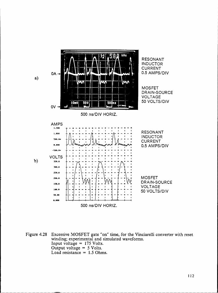
1
T IHRE ‘ ‘ ""'“ g RESONANTiT ¤ moucrosz~7 ·%* 7 cuRRENT7* VllällVOA_>·_ I
’ ‘ I I,‘ O.5 AMPS/DIV7·> „ äßlllü I- 7.
I MOSFET7 DRAIN-SOURCET„... VQLTAGEi Tgg U 5gU 5g °‘ ÖÜ VOLTS/DIV
OV500
ns/DIV HORIZ.AI\/IPS
1.006 ÄTÄTÄ RE$ONANT'NDUCTORCURRENT
'·°°°‘f
I‘
If‘
I 7 I I I ° I ° I 0.5 AMPS/DIV
VOLTS 'T°T°T'T'T°T'T°T°T'Tb)JSG.!368.0 -4- ·+-+- +-4--+-
—·+
250.0 —+ -+-4-- +-+- - -4-
-l i-i -l-l MosrsrISM _; L _ _ Q _ I DRAIN-SOURCE¤ • _ L _ • VOLTAGE‘ . T ‘ . T 60 vous/mv
500 ns/DIV HORIZ.
Figure 4.28 Excessive MOSFET gate ”on" time, for the Vinciarelli converter with resetwinding; experimental and simulated waveforms.Input voltage = 175 Volts.Output voltage = 5 Volts.Load resistance = 1.5 Ohms.
112

To summarize the preceding paragraphs, when operating the Vinciarelli converter withreset winding, the following cautions should be observed to avoid nonzero-currentswitching. The normalized output current should be less than unity so that theresonant-inductor current can naturally return to zero. The MOSFET should be turnedoff soon after the resonant-inductor current returns to zero to avoid the peakmagnetizing current from becoming too large and to avoid a second conduction cyclefrom beginning. The loop formed by the resonant capacitor and freewheeling diodeshould be physically small to prevent parasitic oscillations caused by stray inductance.Finally, the maximum switching frequency cannot be too great or the transformer willnot have enough time to completely reset. Usually, for a 1:1 turns ratio between theprimary and the reset winding, the switching frequency should not exceed half of theresonant frequency.
4. THE VINCIARELLI CONVERTER 113

5. THE SECONDARY-RESONANCE E
I FORWARD CONVERTERl
In the previous chapter it has been shown that unless external circuitry is added to the
Vinciarelli converter, the transformer flux reset will be dependent on parasitics. Also,
the Vinciarelli converter only operates in half-wave mode which results in a strongdependence of dc voltage gain on the load. In contrast, the secondary-resonance
forward converter [ll] can operate in full-wave mode or half-wave mode. lt will beshown that in full-wave mode the dc voltage gain of the secondary-resonance forward
converter is almost insensitive to the load. This means, for an application where the loadresistance can vary over a wide range, the secondary-resonance forward converter hasan advantage over the Vinciarelli converter in the following respect. The switching
frequency of the Vinciarelli converter must vary over a wide range to achieve loadregulation whereas the secondary-resonance forward converter in full-wave mode canachieve load regulation by very small variations in the switching frequency. Anotheradvantage of the secondary-resonance forward converter is that the transformer flux is

1
reset by the resonant capacitor; therefore, no external reset circuitry is required and theconverter does not depend on parasitics for flux reset.
Section 5.1 discusses the circuit operation and the topological stages of thesecondary-resonance forward converter. A dc analysis is performed in Section 5.2.Expressions for the voltage and current stresses on the devices are presented in Section5.3.
5.1 Circuit Operation and Topological Stages
Figure 5.1 shows the secondary-resonance forward converter. The dashed connectionof the antiparallel diode across the MOSFET and blocking diode indicates the possibilityof either full-wave or half-wave operation. To facilitate analysis, an equivalent circuitfor the converter is shown in Figure 5.2. The components on the primary side of thetransformer have been reflected to the secondaiy side and are indicated here with a primemark (’). The magnetizing current, IM, is referred to the secondary. In this converter,the magnetizing current is assumed to be a constant dc current, the value of whichdepends on the operating conditions. This will be discussed further at the end of thissection. Also, the filter-inductor current is assumed constant and is modeled by the dccurrent source, IO. The simple on—off switch in Figure 5.2 represents the MOSFET andblocking diode (and the antiparallel diode in full-wave mode). Referring back to thecircuit implementation in Figure 5.1, the series diode and freewheeling diode form adiode-OR configuration. This can be represented as a double-throw switch where itsposition is determined by the polarity of the resonant-capacitor voltage. The
5.THE SECONDARY-RESGNANCE FORWARD coNvERTr:R iis
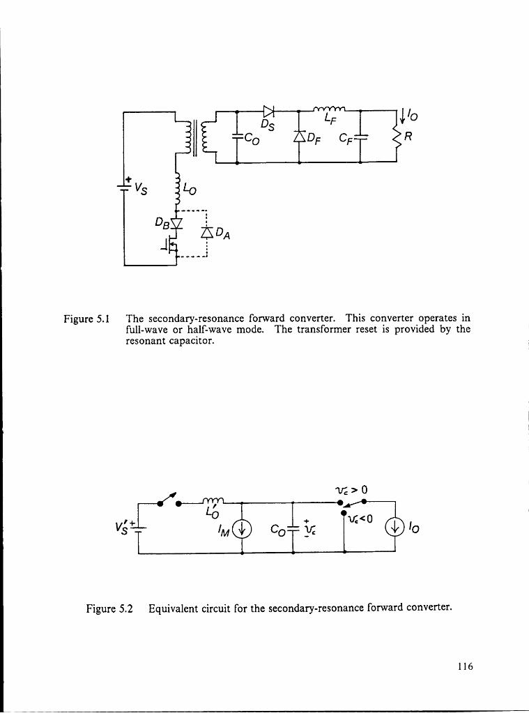
I
> 10CO A R
+ Vs LoDBJ
2
Figure 5.1 The secondary·resonance forward converter. This converter operates infu11-wave or half-wave mode. The transforrner reset is provided by theI'€SOI13.I1( C8p8.C1IOI'.
, vz > 0I
I+LO
+ m<0VS /114 Oo P? IO
Figure 5.2 Equivalent circuit for the secondary—resonance forward converter.II
116 I
III
double-throw switch is used in Figure 5.2 to make the circuit operation easier tounderstand.
The secondary-resonance forward converter in half-wave mode cycles through the four
topological stages shown in Figure 5.3. In this figure, a discussion of the circuit
behavior during each stage is given. The corresponding waveforms for half-wave mode
are shown in Figure 5.4. In full-wave mode the converter cycles through the four stages
shown in Figure 5.5. The first and third stages are identical in full-wave mode. Figure
5.6 shows the waveforms for full-wave mode. Note that in both full-wave and half-wave
mode the resonant-capacitor voltage is negative during a portion of the switching period,
unlike the converters discussed in earlier chapters. In fact, the average
resonant-capacitor voltage must be zero since the resonant capacitor is in parallel with
the transformer which requires volt—second balance. The following paragraphs discuss
the transformer reset mechanism for this converter.
The flux in the transformer core is not reset in the same way as in the Vinciarelli
converter. Here, the flux does not necessarily return to zero but, rather, adjusts its dc
level to maintain volt-second balance on the transformer in the following manner. If the
transformer experiences positive volt-seconds over a switching cycle, the dc magnetizing
current will increase. This increase in IM will cause the resonant-capacitor to charge
more negatively during the fourth topological stage. This decreases the volt-seconds on
the capacitor. Since the capacitor is in parallel with the transformer, this is equivalent
to reducing the volt-seconds on the transformer. Sirnilarly, if the average transformer
volt-seconds become negative, the average resonant-capacitor voltage will increase,
forcing the average transformer voltage back to zero. In summary, this converter
5. THE SECONDARY-RESONANCE FORWARD CONVERTER ll7

TIME EQUIVALENT INITIAL CIRCUIT FINALINTERVAL CIRCUIT CONDITIONS BEHAVIOR CONDITIONS
• Stage begins when activeswitch is turned on (by control
L6 {L = 0 circuit). (L > 0*' I
[TO · T1] V5 IM CO • Circuit begins in resonance.VC < 0 • ill and vc are increasing. VC = 0
• Stage ends when vc = 0.
, • Circuit is still in resonance.LO ill > o ks d h ill = o* 1 • i increases, pea an t en[T1 - T2] Vs IM0 C 0 /0 dlecreascs.
VC = 0 • Stage ends when i{_ = O. VC > 0
L6 [1, = 0 • Rcsonant capacitor linearly {L = 0[T2 - T3] [M CO [O discharges.
vc > 0 • Stage ends when vc = 0. vc = O
• Resonant capacitor continuesL6 { = 0 to linearly dischargc, but at a { = 0L slower rate. L
_ 0• Stage ends when active switch < 0VC is turned on (by control VC
circuit).
Figure 5.3 Topological stages of the half-wave secondary-resonance forward converter.
1 18

i
Rssom-mr nmoocroa cumaswr
Rssomm cA¤=>Ac¤roR vomxcs„ 'Ä ÄMosrsr DRA|N—SOURCE votmcs
Ü n
Figure 5.4 Waveforms for the half-wave secondary—resonance forward converter.
119

I
TIME EQUIVALENT INITIAL CIRCUIT FINALINTERVAL CIRCUIT CONDITIONS BEHAVIOR CONDITIONS
• Stage begins when activeI switch is turned on (by control
+ ,LO [L = Q circuit). [L > Q[TQ • T1] VS IM Co • Circuit begins in resonance.
VC < 0 • {L and vc arc increasing. VC = 0• Stage ends when vc = 0.• Circuit is still in resonance.
’ _ • {L incrcases, peaks, decreases,LO I1, > 0 becomes negative, and then iL < O
vc = 0 • vc incrcases, peaks, and then VC = Qdecreases.
• Stage ends when vc = 0.
, • Circuit is still in resonance. _. LO [L < 0 IL = Ü[T2 _ T3] *V§ IM CO • vc is negative and decreasing.
VC = 0• {L is negative and increasing. VC < Q• Stage ends when {L = 0.
, _ • Resonant capacitor linearly _ _LO IL = 0 discharges. 'L “ 0
[T3 ' T4] [M CO • Stage ends when active switchvc < 0 is turned on (by the control vc < 0
circuit).
Figure 5.5 Topological stages of the 1"u11—wave secondary-resonance forward converter.
120

RESONANT INDUCTOR CURRENT
RESONANT CAPACITOR VOLTAGE0 'Ä ÄMOSFET DRAIN-SOURCE VOLTAGE
Figure 5.6 Waveforms for the 1”u1l·wave secondary—resonance forward converter.
121

possesses an inherent feedback mechanism which forces the average volt-seconds on thetransformer toward zero and, therefore, prevents the transformer core from saturating.
The dc analysis undertaken in this chapter assumes that the magnetizing inductance ofthe transformer is large enough that the magnetizing current variation is very smallcompared to its dc value. This implies that the transformer flux variation is smallcompared to its dc value and the flux remains in the first quadrant of the B-1-1characteristic. Therefore, it is assumed that the transformer in this converter is designedto store energy in a manner similar to the flyback converter. If the magnetizinginductance is low enough, the transformer flux can enter the third quadrant. In thiscondition the secondary-resonance forward converter encounters different modes ofoperation, one of which is discussed in Reference [19].
5.2 DC Clzaracteristics
The dc analysis of the secondary-resonance forward converter consists of solving thestate equations for each of the topological stages, matching boundary conditionsbetween the stages, and requiring volt-second balance on the transformer. The resultsare then determined numerically in terms of the normalized parameters shown in Table1.1. The details of the analysis are given in Appendix B.
Figures 5.7 and 5.8 show the dc voltage gain for the converter in half-wave mode andfull-wave mode, respectively. These normalized plots assume a transformer turns ratioof 1:1. For other turns ratios, the voltage gain read from the plots must be multiplied
5. THE SECONDARY-RESONANCE FORWARD CONVERTER 122
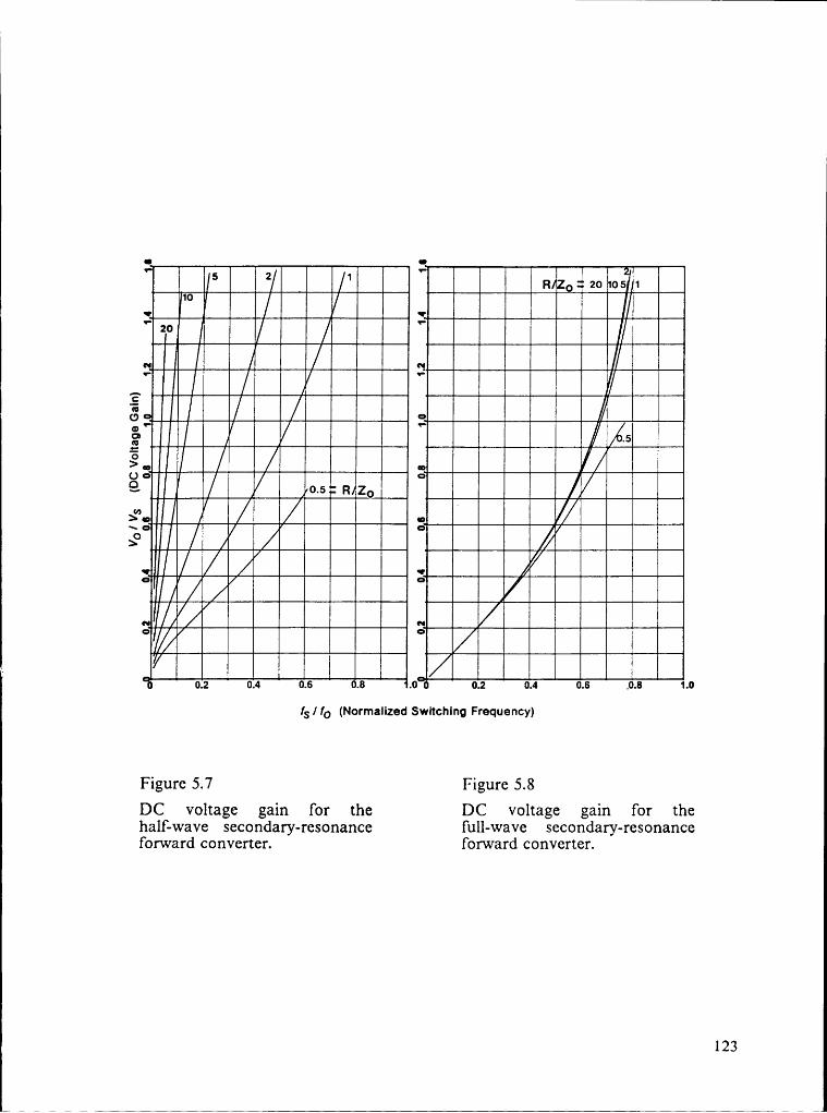
II II I
IIBIFIIIIIII IIIIIEMEMIIIHIIIIIIIII IIIIIIIIHIIHIIIIHIUIII IIIIIIIIMIIIIIIIIIIIMIII IIIIIIIMIIg IIIIIIIIIIIIII IIIIIIIWII2 IIIIIIHIHIIII IIIIIIMIIIIIIIIIIIHIIII IIIIIIMEIIIIMIHIHIIIII IIIIIIMIIIQ Illlßlll ..,2 IIIIIWHIIIIMIIHIHIIII IIIIIMIIII2 IIIMIIMIIIII IIIIMIIIIIIIIIHHQIIIIII IIIZZIIIIIIIIHQIIIIIII IIIHIIIIIII/MZIIIIIIII IIHIIIIIIIWIIIIIIIII IHIIIIIIII—
_Ü----.-I-. _!--II--I.-• 0.2 0.4 0.6 0.8 .0 ¤ 0.2 0.4 0.6 ,0.8 1.0
fs / fo (Normalized Switching Frequency)
Figure 5.7 Figure 5.8DC voltage gain for the DC voltage gain for theha1f—wave secondary·resonance fu1l—wave secondary·resonanceforward converter. forward converter.
123

by NS/NP to get the actual voltage gain. Also, to account for the turns ratio of thetransformer, the following assignments are used to determine the normalized parametersfor the graphs of Figures 5.7 and 5.8.
ä —>fs2¤„/7E%;— <5— 1>Né t ‘2 ‘ 2)
The half-wave mode is more load dependent than the full-wave mode, as was the casefor the buck QRC, because excess resonant tank energy is returned to the input voltagesource in full-wave mode. lt is observed that the dc voltage gain in full wave mode(Figure 5.8) is much less load dependent than that of the Vinciarelli converter (whichhas the same characteristics as the half-wave buck QRC, as shown in Figure 2.3a).
An interesting difference in the dc characteristics between the buck QRC and thisconverter is that this converter is able to achieve a dc voltage gain greater than unity,even with a 1:1 transformer turns ratio. This is due to the transformer magnetizinginductance which introduces a boost function in this converter. It is not normallydesirable to operate the secondary-resonance forward converter in its boost modebecause, in this condition, a high switching frequency is required which causes the dcmagnetizing current to increase dramatically. This can be observed on the plots ofFigure 5.9 for half-wave mode and Figure 5.10 for full-wave mode. Also, as theswitching frequency is increased, the peak drain-source voltage on the MOSFETincreases, as illustrated in Figures 5.11 and 5.12 for half-wave and full-wave mode,respectively. If the secondary-resonance forward converter is operated in full-wavemode with a switching frequency of less than half of the resonant frequency, the peak
5. THE SECONDARY-RESONANCE FORwAR0 cowvrzrrrrzrz 124

I
IWIIIIHHI ‘ =“"-’¤ I IIIIIIIIIIIIIIllgilllllll IIIIIIIIIIIIIII5 IIII IIIIIIII IIIIIIIIIIIIIIE IIIIIIIIIIIII IIIIIIWIIIIIIIIIIMIIIINIIII IIIIIIHIIIIIIIIIIIIIIHIIHIII IIIIIIVIIIIIIIIIHIIIIIII IIIIIHHIIIIIIIMIIIIIIII IlläßßlißßäélIMIIIIIIII IIIIZZIHVII-@lIIIIII IIII
G 0.2 0.4 gi fo (N§r?naIized1S?•v1tchingofäequengyz0-6 0.8 1.0
Figure 5.9 Figure 5.10Normalized dc magnetizing Normalized dc magnetizingcurrent for the half-wave current for the fu11—waveCOI1V€1'I€I°. COIIVCIIGT.
EIWIIYHIIIIII IIIIIIIIIII‘IIlIIIIIII IIIIIIIIIIII IIHIIIIIII IIIIIIIIIAISSIIIIHIIIIIII IIIIIIIIUIIIIIIIIIIIII IIIIIIIWIIIIMIIIIIIII IIIIIIIMÄIIMIIIKI 0.5 -50/z.,I%lIIIIIII I.!5%lIIIIIl
fs / fo (Normalized Switching Frequency)
Figure 5.11 Figure 5.12Normalized peak drain-source Nonnalized peak drain—sourcevoltage on the MOSFET for the voltage on the MOSFET for thehalf-VVBVC SCCOI1d21I’y-ICSOHHIICC fU1l—W6.V€ S€COH(1ä1'y·I'€SOI1El1’1C€fOI'W21I'd COI1V€l’[CI‘. 1~OfWafd COIIVCIIET.
125

voltage on the MOSFET and the dc magnetizing current will not become excessivelylarge.
5.3 Device Voltage and Current Stresses
Many of the device stresses are functions of the dc operating point in thesecondary—resonance forward converter. For these cases, the stresses can be found bynumerical methods. Fortunately, this has already been done, indirectly, in the previoussection. The graphs of normalized magnetizing current and normalized peakdrain-source voltage (Figures 5.9 through 5.12) can be used to find all other voltage andcurrent peaks in the circuit. This is accomplished by use of the state plane, shown inAppendix B, Figures B.2 and B.6, for half-wave and full-wave mode, respectively. Thestate plane describes the behavior of the resonant-inductor current andresonant-capacitor voltage. All other voltages and currents in the circuit can be foundin terms of these two state variables. To completely describe the state-plane trajectory,the following parameters are required:
VDSPN Normalized peak drain-source voltage on MOSFET.= Vcozv '*' 1
[MN Normalized dc magnetizing current
ION Normalized dc output current
Of these parameters, VDSPN and [MN are found from the graphs of Figures 5.9 through5.12. ION is found by:
5. THE SECONDARY-RESONANCE FORWARD CONVERTER 126

I
I L ’C[ON = (5 — 3)s
To simplify the equations for the device stresses, an expression for rz (see Figures B.2and B.6) is given.
rz = /(„/[MN + VDSPN — 1 — [0N)* + 1 <5 — 4>
The following paragraphs give expressions for the device stresses in terms of the circuitparameters and the values of VDSPN, [MN , [ON, and rz.
Peak Voltage Stress on Transistor: The normalized peak voltage stress on the transistorswitch has been found in the previous section. To find the actual peak voltage acrossthe switch, the normalized value is multiplied by the source voltage.
PEAK VOLTAGE STRESS ON TRANSISTOR = VDSPN VS (5 — 5)
DC Magnetizing Current: The normalized dc magnetizing current, [MN, has been found. in the previous section. The actual value of the dc magnetizing current as referred to the
primary is found using,
DC MAGNETIZING cuRRE1~1T = [MN Vs LV; (6 _ 6)(referred to primary) \/E NP
Peak Current Through Transistor: The peak transistor current is equal to the peakresonant-inductor current. From the state plane, in terms of normalized parameters, itis equal to rz + ION + IMN. To account for the normalization and the turns ratio,
5.THE SEOONDARY-RESONANCE FORWARD CONVERTER 127

I
PEAK CURRENT _ V5 N5 _THRouo1—1 TRANSISTOR °° V2 + ION (5 7)
Peak Current in Antiparallel Diode: This applies only to the full-wave mode
implementation, since the antiparallel diode does not exist in half-wave mode. The peak
current in the antiparallel diode is equal to the peak negative value of the
resonant-inductor current. In terms of normalized parameters, this is:
rz — ION — IMN. Therefore, the the actual value of the peak current is:
PEAK CURRENT IN V NANTI-PARALLEL DIODE = (rz — ION — IMN)———..};.——]$ (5 — 8)(full-wave mode only) CO P
Peak Voltage Across Series Diode: The peak voltage across the series diode, DS, is equal
to the peak negative value of the resonant—capacitor voltage. In terms of normalized
parameters it is: , /(VCON + l)2 + IÄIN . The actual value of the peak voltage is:
PEAK VOLTAGE ACROSS _ 2 2 NS _sizmßs DIODE (DS) ” ~/ VDSPN + [MN V5 Tx; (5 9)
Peak Voltage Across Freewheeling Diode: The peak voltage across the freewheeling
diode, DF, is equal to the peak positive value of the resonant-capacitor voltage. From
the state plane, this is: rz + 1, normalized. The actual value of the peak voltage is:
PEAK VOLTAGE ACROSS _ NS _1=REEw1—1EE1.1NG Diooe (DF) ‘ V2 + [) VSK [5 [0)
5. THE SECONDARY-RESONANCE FORWARD CONVERTER 128
_ _

‘ 1
Peak Current Through Series Diode and Freewheeling Diode: The peak current throughDS and DF is equal to the output current. Ideally, one and only one of these diodes ison at any given time. When either diode is on, it conducts the output current.Therefore,
PEAK CURRENT THROUGH DS = [O (5 — 11)
PEAK CURRENT THROUGH DF = IO (5 — 12)
The method that has been used in this section is now summarized. All the Voltage andcurrent stresses on the devices in the secondary—resonance forward converter can bedeterrnined explicitly from: the circuit parameters; the input voltage; the output current;the values of the normalized magnetizing current, [MN; and the normalized peakdrain-source Voltage on the MOSFET, VDSPN• These last two parameters can only befound by implicit equations, which are solved numerically. The results of the numericalsolution of these paramßtßrs have been plotted in Section 5.2 and can be applied to theequations given in this section to determine the peak stresses on the other components.
S. THE sEcONDARY—RESONANcE FORWARD CONVERTER 129

The major results of this thesis are summarized in Section 6.1. Avenues for Further studyare suggested in Section 6.2.
6.1 Summary of Results
6.1.1 The Quasi-Resonant Buck Converter
• In full-wave mode with the output lightly loaded, the dc output voltage increasesas losses in the resonant tank are increased. [Figure 2.6]
• In full-wave mode with the output heavily loaded, the dc output voltage decreasesas losses in the resonant tank are increased. [Figure 2.6]
• In half-wave mode, the dc output voltage always decreases as losses in the resonanttank are increased, regardless of the load. [Figure 2.5]
6. cowcwsrows 130

( 1
• The dc voltage gain is sensitive to the load in half-wave mode but almost insensitiveto the load in full-wave mode. [Figures 2.3 and 2.4]
• The efficiency is almost insensitive to the load in half-wave mode but very sensitiveto the load in full-wave mode. [Figures 2.5 and 2.6]
• Simple, approximate expressions have been derived to predict dc voltage gain andefliciency. [Equations (2-4), (2-17), (2-21) and (2-31)]
• To maximize converter efliciency, ideally, the characteristic impedance should bemade equal to the minimum load resistance divided by the maximum dc voltage gainrequired. [Equation (2-40)]
• An expression for the theoretical maximum converter efficiency possible atmaximum load and minimum input voltage, given fixed values of ESR, has been
· derived. [Equation (2-55)]
6.1.2 The Vinciarelli Converter
• The Vinciarelli converter only operates in half-wave mode. [Section 4.1]
• More topological stages are encountered as compared to the buck QRC. [Figures4.3 and 4.22]
• The dc voltage gain characteristic is virtually identical to that of the buck QRC inhalf-wave mode (multiplied by the transformer turns ratio). [Section 4.1.4]
• The dc voltage gain is sensitive to the load. [Section 4.1.4 and Figure 2.3a]
6. CONCLUSIONS 131

• The Voltage stress on the transistor is higher than for a buck QRC with the same 1input Voltage. [Section 4.1.3]
• The transformer flux will be reset due to parasitics if no additional reset circuitry isadded. [Section 4.1]
• When parasitics are used to accomplish reset, the Voltage stress on the transistor isdependent on the values of certain parasitics. An equation has been derived topredict this stress. [Equation (4-15)]
• A simple passive network consisting of a diode and tertiary transformer winding canbe added to the converter to accomplish a more controlled reset. [Section 4.2 andFigure 1.2c]
• When the tertiary winding scheme is used to reset the transformer, the peak Voltageon the transistor can be clamped to a predetermined value which depends on theratio of primary turns to tertiary turns. [Section 4.2]
• A practical circuit has been implemented in the laboratory. [Section 4.2.2 andFigure 4.23]
• Suggestions to avoid undesirable operating conditions have been presented. [Section4.2.2]
6.1.3 The Secondary-Resonarrce Forward Converter
• The transformer llux is reset inherently within the converter topology; no externalreset circuitry is required and the reset is not dependent on parasitics. [Section 5.1]
6. CONCLUSIONS 132

I
I• The converter can operate in full-wave or half—wave mode. [Section 5.1]
• In full-wave mode the dc voltage gain is almost insensitive to the load. [Figure 5.8]
• In half-wave mode the dc voltage gain is sensitive to the load. [Figure 5.7]
• Unlike the buck QRC, the dc voltage gain of this converter can exceed unity (evenfor a 1:1 transformer turns ratio). [Figures 5.7 and 5.8]
• The dc magnetizing current and transistor voltage stress are dependent on the dcoperating point. [Figures 5.9 through 5.12]
• The voltage and current stresses for all components have been derived. [Section 5.3]
6.2 Suggestions for Further Study
6.2.1 The Quasi-Resonant Buck Converter
· The dc voltage gain and efficiency analysis of Chapter 2 assumed that the filter inductoris large enough so the filter—inductor current can be assumed constant. Usually thiscondition is satisfied. However, the question arises, "What is the smallest value of filterinductor which can be used?" It is shown in Reference [14] that when the inductancebecomes too low the converter enters other modes of operation. lt is desirable to makethe filter inductance as small as possible while meeting the output-voltage ripplespecification without entering other operating modes. lf this causes the
6. c0Nc1.Us10Ns 133

° I
filter-inductor-current ripple to become significant, compared to the dc output current,the dc voltage gain analysis will become less accurate. Therefore, it is desirable toperform a dc analysis of the quasi-resonant buck converter which includes effects due toparasitic losses and a finite filter inductance. The analysis will become more difficult,since the order of the system will increase from two to three.
The effect of parasitic losses on the dc voltage gain and efficiency has beendemonstrated. Another effect of losses, which was discussed briefly in Section 2.2, is thechange in mode boundaries. As the losses are increased, the region in which theconverter can operate, while remaining in the desired mode (also called Mode 1), willbecome smaller [20]. It would be helpful to have an explicit expression or graph whichindicates for what values of circuit parameters the converter will operate in Mode 1 whenlosses are included. The circuit parameters could be, for example: switching frequency,load resistance, and parasitic resistance (where all of these parameters would benormalized).
6.2.2 The Vinciarelli Converter
The topological mode sequences described, in Section 4.1.1 for the parasitic transformerreset scheme and in Section 4.2.1 for the tertiary winding reset scheme, are typical forthese converter implementations. However, variations in circuit components, operatingconditions, and parasitic elements can cause other topological modes to be encountered.
A study should be performed to determine what other modes can exist and which, if any,
are to be avoided. This would include an analysis of the dc characteristics in other
modes. Most likely, the voltage stress on the transistor, as derived in Section 4.1.3, willnot apply to other operating modes.
6. CONCLUSIONS 134

I
Two methods of resetting the transformer’s core in the Vinciarelli converter werediscussed in this thesis. In general, there is a trade-off between the peak voltage stresson the transistor and the time needed to reset the transformer. This is becausevolt-second balance on the transformer is required, and the voltage peak on thetransformer is closely related to the peak voltage on the switch. An "optimal" resetscheme was briefly mentioned in Chapter 3, which is more complex and costly thanthose analyzed in Chapter 4. It would be beneficial to search for other simple resetschemes which would provide near-"optimal" resetting of the transformer's core.
6.2.3 The Secondary-Resonance Forward Converter
In Chapter 5, a dc analysis was performed for the secondary-resonance forwardconverter. This analysis assumed that the transformer magnetizing inductance was largeenough so the magnetizing current can be assumed constant, which is a validapproximation for this converter in many cases. However, it is desirable to reduce themagnetizing inductance of the transformer as much as possible to reduce its size. As themagnetizing inductance is reduced, the constant magnetizing current assumption is nolonger valid causing the dc analysis to become inaccurate. A dc analysis which includesthe effects of finite magnetizing inductance, therefore, would provide results that wereapplicable to more practical converter designs.
To improve the dc analysis, the effects of parasitic losses on the dc voltage gain andefficiency should be included for this converter. In addition, the effects of finite filterinductance should be studied, since the analysis of Chapter 5 assumes an infinite filterinductance. Also, an investigation of the various topological modes possible, and the
mode boundaries between them, should be undertaken.
6. CONCLUSIONS rss

lIn this work, exact results for the dc voltage gain, dc magnetizing current, and peakdrain-source voltage on the MOSFET were computed by solving implicit equations. Itwould be desirable to derive approximate, explicit equations for these parameters, usingmethods similar to those used for the buck QRC, in Section 2.4.
An ac small-signal analysis will be necessary to evaluate the control scheme required forthis converter. It is believed that the control-to-output transfer function will contain aright-half-plane zero due to the boost function provided by the magnetizing inductance.Also, the large-signal transient response of the converter to step-line and step-loadchanges should be analyzed.
6. CONCLUSIONS 136

[1] K. Liu and F.C. Lee, "Resonant Switches: A Unified Approach to Improving
Performances of Switching Converters," INTELEC 84, IEEE Publication
84CI—I2073~5, pp. 344-359.
[2] K.Liu, R. Oruganti and F.C. Lee, "Resonant Switches: Topologies and
Characteristics," IEEE Power Electronics Specialists Conference, PESC 1985
Record, IEEE publication 85CH2117-0, pp. 106-116.
[3] K.Liu and F.C. Lee, "Zero-Voltage Switching Technique in DC/DC
Converters," IEEE Power Electronics· Specialists Conference, PESC 1986
Record, IEEE publication 86CH2310—1, pp. 58-70.
[4] R. Tymerski and V. Vorperian, "Generation, Classification and Analysis of
Switched-Mode, DC-to-DC Converters by the Use of Converter Ce1ls," IEEE
International Telecommunications Energy Conference, 1986, pp. 181-195.
REFERENCES 137

1
[5] P. Vinciarelli, "Forward Converter Switching at Zero Current," U.S. Patent,4,415,959 Nov. 1983.
[6] E. Miller, "Resonant Switching Converter," U.S. Patent, 4,138,715 Feb. 1979.
[7] M. Jovanovic, K. Liu, R. Oruganti, F.C. Lee, "State-Plane Analysis of
Quasi-Resonant Converters," IEEE International Telecommunications EnergyConference, pp. 235-242, 1985.
[8] S. Cuk and R.D. Middlebrook, "A New Optimum Topology Switching
DC-to-DC converter," IEEE Power Electronics Specialists Conference, 1977
Record, pp. 160-179 (IEEE Publication No. 77CH12l3-8).
[9] A. Pietkiewiecz and D. Tollick, "Systematic Derivation of Two-State Switching
DC-DC Converter Structures," IEEE International Telecommunications Energy
Conference Record, pp. 473-477, Nov. 1984.
[10] N.R.M. Rao, "A Unifying Principle behind Switching Converters and Some New
Basic Configurations," IEEE Transactions on Consumer Electronics, pp.
142-148, Feb. 1980.
[ll] K. Liu and F. Lee, "Seconda1y-Side Resonance for High-Frequency Power
Conversion," IEEE Applied Power Electronics Conference, pp. 83-89, 1986.
[12] L.W. Nagel, "SPICE2: A Computer Program to Simulate Semiconductor
Circuits," Memo ERL-M520, Electronics Research Laboratory, University of
California, Berkeley, May 1975.
REFERENCES 138
_ „ _

[13] J.C. Bowers and 1—I.A. Nienhaus, "SPICE—2 Computer Models for HEXFETS,"International Rectifier Power MOSFET I—IEXFET Databook, 1985, ApplicationNote 954A, pp. A-153 through A-160.
[14] R. Tymerski, "Finite Filter Inductance Effects on Quasi-Resonant ConverterPerformance," VPEC Power Electronics Seminar, Blacksburg, Virginia,November, 1986, pp. 24-36.
[15] V. Vorperian, "Ana1ysis of Resonant Converters," Ph.D. Thesis, CaliforniaInstitute of Technology, May 1984.
[16] Private Communication with V. Vorperian, November, 1986.
[17] V. Vorperian, "Design and Analysis of DC-to-DC Resonant Converters,"Annual Report for the International Business Machines Corporation, Owego,NY, under Contract No. 85-0513-10, June, 1986. ·
[18] P. Vinciarelli, "Optimal Resetting of the Transformer's Core in Single-EndedForward Converters," U.S. Patent, 4,441,146 Apr. 1984.
[19] K. Liu, "I—1igh—Frequency Quasi-Resonant Converter Techniques," Ph.D.Dissertation, Virginia Polytechnic Institute and State University, October, 1986.
[20] Private Communication with R. Oruganti, October, 1986.
REFERENCES 139

i APPENDIX ADERIVATION OF DC VOLTAGE GAIN AND EFFICIENCYOF THE QUASI-RESONANT BUCK CONVERTER
WITH PARASITIC LOSSES
The results of the derivation given in this appendix are used in Section 2.2 of this thesis.
Symbols used in this appendix are defined in Table A.1, in addition to the previousdefinitions given in Table 1.1.
A.1 Statement of Problem
GIVEN: The quasi-resonant buck converter (using the L-type zero-current switch), withresonant—inductor ESR and resonant-capacitor ESR, shown in Figure A.1; and,
APPENDIX A 140

Table A.1 Definition of symbols used in Appendix A.(See also definitions in Table 1.1.)
¤ = <¤/(2 QLC)A = T1/QLCb =(ÜB
1 = 2 TI SOC Resonant capacitori(J) Resonant—inductor currentII DC input current[IN Norrnalized dc input current
in Resonant-inductor current during Stage n (n = 1,2,3,4)iN„ Normalized resonant-inductor current during Stage n (n = 1,2,3,4)
L Resonant inductorQc = Z0/RcQL = ZO/RLQLC = Z0/(RL + Rc)SQ = N/1 · [1/(2 QLc)]2tn Tirrre interval for nm topological stage (n = 1,2,3,4)JN Normalized time
= J/TOTN„ Normalized time interval of nm stage (n = 1,2,3,4)
= J„co/(27:) = J„/TOTS Switching periodTSN Norrnalized switching period
= TS/TO = FO/FSv(J) Resonant-capacitor voltagev„ Resonant-capacitor voltage during Stage n (n = 1,2,3,4)vN„ Normalized resonant·capacitor voltage during Stage n (n = 1,2,3,4)
vO Voltage across the resonant capacitor and its ESRVON DC voltage gain
VX Resonant-capacitor voltage at the beginning of Stage 3VXN Normalized resonant-capacitor voltage at the beginning of Stage 3
= Vx/ Vs
14 1

I
l_ RL LFIJ RI Rvs C Rvi C
Figure A.l The buck quasi-resonant converter including parasitic losses in theresonant Iällk.
L RL
Rcll R
Vs Io° vi C
Figure A.2 Equivalent circuit for the buck quasi-resonant converter including parasiticlosses in the resonant tank.
142

GIVEN:FS/FO Normalized Switching FrequencyR/ZO Normalized Load ResistanceCL Normalized Resonant-Inductor ESRCC Normalized Resonant-Capacitor ESR
DETERMINE:VONn
Efliciency
ASSUMPTIONS:
1) The tilter inductance, LF, is large enough that the filter-inductor current canbe considered a constant dc value equal to the load current, IO. This simplifies the gequivalent circuit, as shown in Figure A.2.2) The circuit is operating in Mode 1, described in Section 2. l. l. This means thatthe resonant-inductor current and the resonant-capacitor voltage both naturallyreturn to zero each switching cycle (without being forced to zero by the switch).
A.2 Overview of Solution
1) Formulate state equations for each topological stage. (The states are:resonant-inductor current and resonant-capacitor voltage.)2) Find the state-transition matrix for each topological stage.3) Determine the time·domain solution of the states during each stage.4) Find an expression for the time interval of each stage.5) Find an expression for the dc output voltage by integrating theresonant-capacitor voltage over a switching cycle.
APPENDIX A 143

1|
6) Find an expression for the dc input current by integrating theresonant-inductor current over a switching cycle.7) Compute efiiciency from previous two steps.8) Formulate equations based on boundary conditions (the states do not changeinstantaneously through a topological stage change).9) Compute the solution using Newton’s method to satisfy the boundaryconditions above.
A.3 Detailed Solution
STEP 1: Formulate state equations for each topological stage. (The states are:resonant-inductor current, i(t), and resonant-capacitor voltage, v(r).)
The topological stages which the quasi-resonant buck converter cycles through areshown in Figure A.3. Also shown in this figure are the state equations describing thecircuit behavior during each stage.
STEP 2: Find the state-transition matrix for each topological stage.
The state-transition matrix, <I>,,(z), is computed by taking the inverse Laplace transformof the inverse of the matrix [sl — A„]. "A,," is the fundamental system matrix for therz-th topological stage, "l" is the identity matrix, and "s" represents complex frequency.This is stated as:
<1>,,(z) = $_l|:(sI - .4,,)*] (A -1)
APPENDIX A _ 144
_ _ _

I
I-Ti"3I
0·
I
~ InI
I
I-;Q I: O
I
I
ILI c
~l Q
Z
“9I-A,
I5
O A
G
Q
2
O
gf•~•
~A
QVj
‘“
*5
LuPQ.,
°G _:
,.3,
IS
I- == O7-
== O*
Q
E
I;o
Ii:
cn\
¢>+
I;-I
6
Ü]I
I————I +>
IO
-1
3
u
A
Ä
>=.’ C:
•-I
II
OG
Q
A·~J -·¤<
oI
IIÄ
-——-—·IQ
"
=I
"
ga 6 ·^"
r_____A'
'•~• "
L)
.3 A
9-33
sa
E
II-
I
IIÖI
-—
I
Q.,
D
CA
O
PE ‘
3
QE
U¤
nu 5
II 6
-
3
Fc'
„9
mq+;
I Q
Q
cu
LU
>gb
~l T
cg
•~
•-bvz
Sr;:5
u.1Ü
oE
’”
E9-
"’I2V7<0I-3-29LL.
1415

‘ 11
Stage I
RL. ·— i 0LA1 = (A " 2)0 0
Re- %t 0‘1’1(¢) = (A · 3)0 1
Stage 2
LL L
A2 = (A " 4)1C 0
e_“tcosbt——äe_°tsi11bt‘Dz(¢)= (A — 5)
Stage 3
0 0 1 0As = 1 (D30) = (A · 6)0 0 0 1
APPENDIXA 146

u¤
Stage 4
0 0 1 0A4 = „ <P4(¢) = (A — 7)0 0 0 1
STEP 3: Determine the time·domain solution of the states during each stage.
For each topological stage, the time-domain solution of the state vector, X(1), is a
function ofi the state—transition matrix, <I>(t); the initial value of the state vector, X(0);
and the input vector, BU. The solution is given by:
iv) ,= X(t) = <D(t) X(0) + .,.0 <I>(t) dt BU (A — 8)v(¢)
Stage I
0X1(0) = (A · 9)0
R4-(1 - ..- 6) 0R1.j'(§<I>(1) dr = (A — 10)
0 z
0 1/L IO VS/LBU = = (A — 11)
O 0 VS 0
APPENDIX A 147

The solution to the state vector is now given by substituting the above expressions intoEquation (A-8), which results in,
- L V$(1 - 1 J1) 11 $X1(t) = L (A — 12)
0 : 0
Therefore, the resonant-inductor current and resonant-capacitor Voltage during Stage 1are, respectively,
V - Li(z) = -I%(1— e Ä') (A -13)1,
v(t) = 0 (A — 14)
Stage 2
IX2(0) = 0] (A ‘ 15)0
, H1 H2(0 <I>(1:) dt = (A — 16)H2 H4
where:
S e’“'sinbtCO 4 QLC co SQ
H2 =———l e‘“'si11bt+———l e‘“‘cosbt————l ‘2coQLCZ0SQ (ÜZO COZO
H3 = - ———g-Q———e""sinbt — —€—Q-e"“cosbt + @2coQLCSQ co co
APPENDIX A 148

I
1
SH4 = —£ — lT;—— e’“‘sinbt — lle’“’cos bt + --1co 4 QLC (0 SQ c0QLC coQLC
BU RC/L 1/L IO — RCIO/L + VS/L (A 17)— 1/C 0 V3 — I0/C
Xm _ P1 P2 IO+
Hl H2 RCIO/L + VS/L(A 18)
P3 P4 0 H3 H4 — I0/C
where:
P = e"“‘cos bt — —$e"“‘sin bt1 2QLCSQ= - Q., — z ·P2 ZOSQ e " sm bt
ZP3 = ——Q—e'“‘sin btSQP = e’“’cos bt + ——l-—e’“’sin bt" 2Q„SQ
Using the previous equations, the resonant-inductor current and resonant-capacitorVoltage for Stage 2 are:
1(1) (A — 19)
(A — 20)
Stage 3
Let V be the initial Voltage on the resonant capacitor at the beginning of Stage 3. VX Xwill remain an unknown until after the final numerical solution is complete.
APPENDIX A 149

0X3(0) = (A · 21)VX
t z 0jo <D(t)d1: = (A — 22)0 z
0 0 IO 0BU = = (A — 23)-1/C 0 VS — IO/C
1 0 0 z 0 0 0X(t) = + = [ (A - 24)0 1 VX 0 t — IO/C VX
—Theresonant-inductor current and resonant-capacitor voltage for Stage 3 is therefore,
i(t) = 0 (A — 25)
[0v(t) = VX — —ö_—t (A — 26)
Stage 4
During Stage 4 the resonant-inductor current and resonant-capacitor voltage are zero. _
i(t) = 0 (A —· 27)
v(t) = 0 (A —— 28)
STEP 4: Find an expression for the time interval of each stage.
This is accomplished by setting the time-domain solution of the states (found in the
APPENDIX A 150

11
previous step) equal to the final value of the states for a particular topological stage andthen solving for the value of time at the end of that stage.
Stage I
At the end of Stage l the resonant-inductor current equals the output current. That is,
V - Lil(tl) = IO = —-‘i(l — eLLt*)
(A — 29)RL
Solving for tl gives,
t1= ——}%l11(l—e—RLI°/VS) (11-30)L
In terms of the normalized time duration for Stage l, TN1,
QL IoivT = — ——ln l — ——— A — 3lNl zu QL ( )
Stage 2 .At the end of Stage 2 the resonant-inductor current equals zero.
0 (A “ 32)
The expression for i2(t) is too complicated to solve analytically for t. Equation (A-32),therefore, becomes one of the boundary equations to be solved numerically. Note thatan additional constraint is necessary to distinguish half-wave mode from full-wave mode.In half-wave mode the slope of the resonant-inductor current is negative at the end ofStage 2, whereas in full-wave mode the slope is positive.
ZTI! < 0 (HALF-WAVE MODE) (A — 33)2
APPENDIX A 151

I
I
0 (FULL·WAVE MODE) (A — 34)*2
Stage 3At the end of Stage 3, the Voltage across the resonant capacitor and its BSR is zero.
*’0(’2) = 0 (A " 35)
Therefore, the resonant-capacitor Voltage minus the Voltage drop across theresonant-capacitor BSR is zero.
v(t3) — IORC = 0 (A —· 36)
or, by substitution,
X C 3 O C
Solving for the time duration of Stage 3,
z — C V — 1 R A — 382 " X 0 c) ( )
The normalized time duration of Stage 3 is given by,
T1V2=;‘* VX1v“@ (A—39)27* ION Qc
Stage 4The time duration for Stage 4 is determined from the expressions already obtained. ltis given by, °
APPENDIX A 152

where TS is the switching period (the time required to complete one cycle through each
of the four topological stages). The above equation will be used as a check to insure that
the resonant-capacitor voltage decreases to zero during each switching cycle. If it does
not, then the converter is not operating in the desired mode (Mode 1). This analysis is
only valid for Mode l operation. The way to insure that the resonant-capacitor voltage
decreases to zero is to impose the constraint that I4 be greater than or equal to zero.
By normalizing the above equation, this constraint becomes,
1TN1+TN2+TN:$—*‘** (/1*41)FS/Fo
STEP 5: Find an expression for the dc output voltage by integrating the
resonant-capacitor voltage over a switching cycle.
The dc output voltage is the average of the resonant-capacitor voltage plus the average
of the voltage across the resonant-capacitor ESR. The average voltage across the
resonant-capacitor ESR is zero because there is no dc current through the capacitor.
Therefore, the dc output voltage may be found by integrating the resonant-capacitor
voltage over the entire switching cycle. The resonant-capacitor voltage is equal to zero
during Stages 1 and 4; so the normalized output voltage (dc voltage gain) is given by,
- 1 TN2 TN:SN
APPENDIX A 153

11
form VN2 dzN TN2( — A sinBTN2 — Bcos BTN2)Z0 A + B2Iorv VB —A T -+———l——-—e N2 —AcosBT +BS1I1BTZO A2 + B2 ( N2 N2)ION B A“” ““ VAQQTT
Awhere,ZO ZO 1 1 1V =———————- —-+——- —Z S —————A SO ZQNSO (Qc ION) A wäcsg)ZO 1 1B Qzc O( Qc IONZ
V = Z L. + L. -LC 0( Qc low) Qrc
ÄOTNB "~3 döv = T~2(Vx1v " Il ION TN3) (A T 43)
STEP 6: Find an expression for the dc input current by integrating theresonant-inductor current over a switching cycle.
The resonant-inductor current is zero during Stages 3 and 4. The normalized dc inputcurrent is, therefore, given by,
. Q — Qform 'Nl 4'Irv (A — 45)
APPENDIX A 154

( l
A Sil]BcosA2+ B2(A — 46)
+ 1 T + 1 1 -!ä°-ON N2 ON A 2 2A + B
where,
1=—;-+-+-)
.5*+;- (A—47)A QLC SQ (Qc ION Q 4 Qäc sQ
STEP 7: Compute efficiency from the previous two steps.
Efficiency is given by,
n = -—- (A — 48)Vs I1
In terms of normalized parameters, the efficiency is,
V2n = -‘?L—
(A — 49)lIN(R/ZO)
An expression for the dc voltage gain, VON, was found in Step 5 and the normalized dcinput current, IIN, was found in Step 6. The normalized load resistance, R/ZO, is a givenparameter.
STEP 8: Form equations based on boundary conditions.
In this step all the work of the previous steps is summarized. The equations, thus far,have been in terms of the given parameters and three unknowns which are:
ION Normalized Output Current
APPENDIX A 1ss

(1
TN2 Normalized Time Duration of Stage 2
VXN Normalized Resonant-Capacitor Voltage at End of Stage 2
After these parameters become known, the dc voltage gain and efüciency can becomputed. To find the above unknowns, three equations are necessary. Theseequations will be stated as functions set equal to zero in preparation for the next step,where Newton’s method is used to solve the equations. The first function is based onthe fact that the dc voltage gain divided by the normalized load-current must be equal
to the normalized load-resistance. That is,
f — R/Z — VON — 0 -1 " 0 —'—‘ " (A $0)[0zv
The second function insures that the resonant-inductor current is zero at the end ofStage 2.
/3 = i1v2(T1~/2) = 0 (A " 51)
The third function states that the normalized resonant-capacitor voltage at the end ofStage 2 is equal to VXN.
/3 = VXN " vN2(TN2) = 0 (A ‘ 52)
Functions j], J}, andß will now be expressed in terms of the given parameters and thethree unknowns listed above.
Function j]
.. _ Vozv _ _fi — R/ZO ——— — 0 (A 53)ION
APPENDIX A 156

R/ZO is a given, and ION is one of the unknowns. VON has been found in Step 5 and issummarized here:
V -VON = ATN2( ' A "'BcosA+ B
V - .AcosBTN2 + BsmBTN2)V B V A+ VK3 TN2 +Ü+ ‘*° TN3(VXN ” nIONTN3)]
where,
ION ION 1 1 1V =————————— ——+i —I S——i——Kl SQ 2 QLO SQ Qc ION ON Q 4 Qäc SQ1 1 IONV = — I —— + — + -—-K3 OA/( Qc [ON) Qz.c
IV = [ L + L - [email protected] °K( Qc ION) QOO
Function _/Q
fi = iN2(TN2) = 0 (A — 54)
where TN2 is one of the unknowns. Normalizing the expression for i2(t), found in Step3, results in,
Qc ION 4 QäC.SO QLO SQ
Function fg
J3 = VXN “ VN2(TN2) = 0 (A ‘ 55)
APPENDIX A 157

VXN and TN2 are two oF the unknowns. Normalizing the expression For v2(t), Found inStep 3, gives
fg = VXN_
VK]Thevariables VK1, VK2, and VK; have been defined above, For the Function j}.
STEP 9: Compute the solution using Newton’s method to satisfy the boundaryconditions above.
Three equations have been Formed,
MX)X F(X) = ß(X) = O (A — 57)
MX)
and there exist three unknowns,
[ow
VXN
Newton’s Method For solving simultaneous nonlinear equations oF several variables isstated as,
X„+l = X,, — [J(X,,)]—1F(X„) (A — 59)
This equation is successively computed until F(X) is "close enough" to zero. Thevariable X,, represents the vector oF variables X on the n-th iteration oF Newton’sFormula. The matrix .](X„) is given by,
APPENDIX A 158

ÖÄ(X„) Öfi(X„) ÖÄ (X11)ÖION öTN2 öl/XN
.. M M)Öß(X„) ÖJE(X„) ÖJS(X„)
./'(Xn) is called the Jacobian matrix, which is essentially the multidimensional derivativeof F(X„). The partial derivatives indicated above will not be computed analytically dueto the complexity of the expressions. Since this method relies on numerical solution, itis expedient to determine these derivatives numerically, also. The partial derivatives areapproximated by,
jlx + Ax) —j(x) (A _ 61)0x Ax
where Ax is a "very small" increment.
All the equations necessary to compute a numerical solution have been established atthis point. A FORTRAN program was written to implement the numerical solution.The program is shown in Figure A.4 and a corresponding flowchart is given in FigureA.5. Observe, in the flowchart, that it is necessary for the user to supply an initial guessfor the unknown variables. This initial guess must be close enough that Equation (A-59)will converge. Instead of only calculating results for a single set of input parameters, the
APPENDIX A 159

C XXX SOLVES DC CHARACTERISTICS OF BUCK RESONANT CONVERTERC XXX NITH RESONANT INDUCTOR AND CAPACITOR ESRC XXX LEN ROUFBERG AUGUST 18, 1986C INPUTS:C FSFO = FS/FO, NORMALIZED SNITCHING FREQUENCYC ROZO = R/ZO, NORMALIZED LOAD RESISTANCEC ZL = NORMALIZED RESONANT—INDUCTOR ESR ( >O )C ZC = NORMALIZED RESONANT—CAPACITOR ESR ( >0 )C UNKNONNS:C ION = NORMALIZED LOAD CURRENTC TN2 = NORMALIZED TIME DURATION OF TOPOLOGICAL STAGE 2C VXN = NORMALIZED RESONANT—CAPACITOR VOLTAGE AT ENDC OF TOPOLOGICAL STAGE 2C RESULTS:C VON = DC VOLTAGE GAINE EFF = CONVERTER EFFICIENCYC INITIAL GUESS FOR ION, TN2, VXN ( HALF—NAVE MODE ):C ION = (FSFO/4+SQRT(ROZOXFSFO/PI))/ROZOC TN2 : 0.5C VXN : 2.0C INITIAL GUESS FOR ION, TN2, VXN ( FULL—NAVE MODE ):C ION : FSFO/ROZOC TN2 : 1.0C VXN : 0.0CC IN STEP 15, THE RELATIONAL OPERATOR MUST BE:C .LE. ( FOR HALF—NAVE MODE )C .GT. ( FOR FULL—NAVE MODE )C
IMPLICIT REALX8 (A—Z)COMMON PI
C PI=3.14159265C XXX INPUT INITIAL PARAMETERS
PRINTX,'ENTER FSFO'READ(6,X)FSFO[ PRINTX,'ENTER ROZO'READ(6,X)ROZOPRINTX,'ENTER ZL'READ(6,X)ZLPRINT*,'ENTER ZC'READ(6,x)ZcQL=1/2.0/ZL
C QC=1/2.0/ZCC XXX INPUT INITIAL GUESS FOR UNKNONNS1 PRINTX,'ENTER INITIAL GUESS FOR ION'READ(6,*)ION
PRINTX,'ENTER INITIAL GUESS FOR TN2'READ(6,*)TN2PRINTX,'ENTER INITIAL GUESS FOR VXN'
C READ(6,X)VXNC XXX CALCULATE FUNCTION VALUES AT POINT (ION,TN2,VXN)
Figure A.4 FORTRAN program to compute the dc voltage gam and efficiency of thebuck quas1—resonant converter.
160

i
i
10 äALé1CALCF(FSFO,ROZO,0L,QC,ION,TN2,VXN,F1,F2,F3,VON,IIN,TOT)A2=F2A3=F3
CC xxx PERTURB ION
ION=ION+0.00lg2L%1CALCF(FSFO,ROZO,QL,QC,ION,TNZ,VXN,Fl,F2,F3,V0N,IIN,TOT)A5=F2A6=F3
C ION=ION—0.001C xxx PERTURB TN2
TN2=TN2+0.001CAL%1CALCF(FSFO,ROZO,QL,0C,ION,TN2,VXN,F1,F2,F3,VON,IIN,TOT)A7=A8=F2A9=F3TN2=TN2-0.001
CC xxx PERTURB VXN
VXN=VXN+0.001§ALLFCALCF(FSF0,ROZO,QL,0C,ION,TN2,VXN,F1,F2,F5,V0N,IIN,TOT)10=
A11=F2A12=F5VXN=VXN—0.001
CSLOPE=A8—A2
C xxx CHECK FOR CORRECT SIGN OF D(F2)/D(TN) 3 TN2C xxx (SLOPE .LE. 0) FOR HALF—NAVE, (SLOPE .GE. 0) FOR FULL—NAVE:
15 IF (SLOPE .LE. 0) GOTO 30PRINTx,'RESONANT INDUCTOR CURRENT IS NON-ZERO'PRINTx,'OR INITIAL GUESS(ES) ARE NRONG'NRITE (6,90) ION, TN2, VXNPRINTx,Fl,F2,F3,VON,IIN‘ 20 FORMAT (2El3.4)STOP
CC xxx CHECK IF RESULT NITHIN TOLERANCE
30 IF (A1xx2+A2xx2+A3xx2 .LT. 0.000001) GOTO 100CC xxx CALCULATE JACOBIAN
J11=(A4—Al)/0.001J12=(A7-A1)/0.001J13=(A1Ü'A1)/Ü.ÜÜ1J21=(A5—A2)/0.001J22=(A8—A2)/0.001J23=(A11-A2)/0.001J31=(A6-A3)/0.001J52=(A9-A5)/0.001J35=(A12—A3)/0.001
CC xxx CALCULATE INVERSE JACOBIAN (XDET)
Figure A.4 (Contiuued)
161

N11=J22XJ33—J32xJ23N12=J32xJ13—J12xJ33N13=J12xJ25-J22xJ15N21=J23XJ51—J2lxJ55N22=J1lXJ33-J31XJ15N23=J21XJ15—J11xJ23N31=J21XJ32-J31xJ22N52=J31xJ12-Jl1xJ52N35=J11XJ22—J21xJ12
C DET=J11xN11+J12xN21+J15xN51C XXX CALCULATE NEN VALUES FOR ION,TN2,VXNION=ION—(A1XN11+A2XN12+A3XN13)/DET
TN2=TN2—(A1XN2l+A2XN22+A3XN23)/DETvXN=vXN-(A1xN51+A2xN32+A3xN33)/DETNRITE (6,90) ION, TN2, VXN90 FORMAT (6E13.4)
C GOTO 10C XXX RESULTS ARE NITHIN TOLERANCE, COMPUTE VON AND EFF100 CALL CALCF(FSFO,ROZO,QL,0C,ION,TN2,VXN,F1,F2,F3,VON,IIN,TOT)EFF=VONxION/IINCC XXX CHECK IF RESONANT CAPACITOR IS DISCHARGING TO ZEROIF (TOT .LE. (1/FSFO)) GOTO 110PRINTX,'RESONANT CAPACITOR IS NOT ABLE TO DISCHARGE TO ZERO'NRITE (6,90) ZL,ION,TN2,VXN,VON,EFF .C STOPC xxx PRINT RESULTS110 NRITE (8,90) FSFO, VON
NRITE (9,90) FSFO, EFFC NRITE (6,90) FSFO,ION,TN2,VXN,VON,EFFC XXX INCREMENT OR DECREMENT RUNNING PARAMETERFSFO=FSFO+.01C XXX CHECK IF RUNNING PARAMETER EXCEEDS DESIRED RANGE1 IF (FSFO .GT. 1.0) STOPC xxx CONVERT FROM Z TO Q
0L=1/2.0/ZL0C=1/2.0/ZCGOTO 10
C ENDE xXX SUBROUTINE TO CALCULATE FUNCTIONS F1, F2, F3, AND VON
SUBROUTINE CALCF(FSFO,ROZO,QL,QC,ION,TN2,VXN,F1,F2,F3,VON,IIN,TOT)IMPLICIT REALX8 (A—Z)C COMMON PIC XXX FIRST CALCULATE INTERMEDIATE RESULTSQLC = 1.0 / ( (1.0/QL)+(1.0/QC) )
S0 = SQRT(1.0—(1.0/2.0/QLC)XX2)A = PI/QLCB = 2.0xP1xSQ
Figure A.4 (Continued)
162

«u1
VK1=IÜN/SQ'IÜN*((1.Ü/Qc)+(1.Ü/IÜN))/2.Ü/QLC/SQVK1=VKl—IONX(S0—1/(4.0XSQXQLCXx2))VK2=-IONX((1.0/QC)+(1.0/ION))+ION/QLCVK5=—VKZI1A=—l.0/OLC/SQ + ((1.0/QC)+(1.0/ION))X(S0+l.0/(4.0*SQ*0LCX*2))TN1=—QLxLOG(1.0—ION/QL)/2.0/PITN5=(VXN'IÜN/QC)/2•Ü/PI/IÜNTOT=TN1+TN2+TN5C
C xxx CALCULATE F1 = ROZO — VON/IONVP1=VK1XEXP(—AXTN2)X(—AXSIN(BXTN2)—BXCOS(BXTN2))/(AXX2+BXX2)VP2=VK2XEXP(—AXTN2)X(—AXCOS(BXTN2)+BXSIN(BXTN2))/(AXX2+BXX2)VP3=VK3XTN2+VK1XB/(AXX2+BXX2)+VK2XA/(AXX2+BXX2)VP4=TN5X(VXN—PIxIONXTN3)VON=FSFOx(VP1+VP2+vP3+VP4)
C F1=ROZ0—VON/IONC xxx CALCULATE F2 = IN2(TN2)FZ=IÜNX(l.O+IlAXEXP(*AXTNZ)XSIN(BXTNZ))CC XXX CALCULATE F3 = VXN — VN2(TN2)
F3=VXN—VK1xEXP(—AxTN2)x$IN(BxTN2)F5=F3—VK2xEXP(—AxTN2)xCOS(BxTN2)—VK3C
C XXX CALCULATE IIN = AVERAGE INPUT CURRENTIIN1=QLx(TN1+QL/2.0/PIxEXP(-2.0xPIxTN1/QL)—QL/2.0/PI)IIN2=IONXI1AXEXP(-AxTN2)X(—AXSIN(BXTN2)—BXCOS(BXTN2))/(AXX2+BXX2)IIN5=IONXTN2+IONXIIAXB/(AXX2+BXX2)IIN=FSFOX(IINl+IIN2+IIN3)RETURNEND
Figure A.4 (Contmued)
163

START
INPUT INITIAL PARAMETERSFx/Fo· R/Zo· Cu Cc
INPUT INITIAL GUESSFOR UNKNOWNS
[om Tan- VXN
CALCU1-ATE No, RUNNING I•ARAME‘I‘6Rmx..>.6<x.>.mx.> EXCEEDS R^NGE ?
PERTURB
INDIVIDUALLY, AND RECALCULATEA-ß•ß
(TO DETERMINE JACOBIAN MATRIX)
dä < 0 (HALF—WAVE MODE)ZTI,} > 0 (I=UI,I,-wAvIz Mom;) ERROR7
COMPUTE DC VOLTAGEGAIN AND EFFICIENCYRESULTS WITHIN _TGLERANGI2 1- FROM '<>~· TM- VIN-Fs/Fo• R/Zo· Cu Cc
CALCULATE 1AcoIa1AN MATRIX, PRWT RESUUSINVERT JACOBIAN MATRIX
INCREMENT RUNNINGPARAMETERFIND NEW VALUES OF (ps/po} R/Za cb W cc)[om Tan- Vxn
USING NEWTON'S FORMULA
Figure A.5 Flowchart for the cdmputation of the dc voltage gain and efficiency of thebuck QU3.Si-1’€SOI18.1’1I COI1VCl’I€I'.
164

program generates a "curve" of solutions where a single parameter (normalizedswitching frequency, for example) is swept over a range of values. When this is done,the user need only input the initial guess of the unknowns for the Hrst point to becalculated. After that, the parameter being swept is incremented in sufliciently smallsteps that the results of each previous solution can be used as the initial guess to thesolution of the new point.
APPENDIX A 165

DERIVATION OF DC CHARACTERISTICS FOR THE
SECONDARY-RESONANCE FORWARD CONVERTER
In this appendix the derivation is given for dc Voltage gain, normalized dc magnetizingcurrent, and normalized peak drain-source Voltage on the MOSFET, for thesecondary-resonance forward converter.
The results of” the derivation given in this appendix are used in Sections 5.2 and 5.3 ofthis thesis. A
Symbols used in this appendix are defined in Table B.1, in addition to the previousdefinitions given in Table 1.l.
APPENDIX B 166

ll
Table B.l Definition of symbols used in Appendix B.(See also definitions in Table 1.1.)
iLN Normalized resonant-inductor current
rl = (See Figures B.2 and B.6)
r2 = , /(N//$71 — ION)2 + 1 (See Figures B.2 and B.6)
r3 = , /(\/Ü — ION)? + 1 (See Figure B.6)
AT„ Time interval for Stage n (n = 1,2,3,4)
TS Switching period
vc Resonant-capacitor voltage
vcN Normalized resonant-capacitor voltage
= vc! VsvON„ Normalized resonant-capacitor voltage during Stage rz (rz = 1,2,3,4)
VON DC voltage gain
91 = sin-] [IMN/rl] (See Figures B.2 and B.6)
92 = cos°‘ [1/rl] (See Figures B.2 and B.6)
93 = sin;] [l/rz] (See Figures B.2 and B.6)
94 = sin" [(IMN + ION)/rz] , in half·wave mode (See Figure B.2)
= sin'} [1/rg] , in full-wave mode (See Figure B.6)
95 = rt/2 — 94 — sin"} [IMN/rg] (See Figure B.6)
167

II
I
I
B.1 Statement of Problem
GIVEN: The secondary-resonance forward converter shown in Figure 5.1; and,
GIVEN:FS/FO Normalized Switching FrequencyR/ZO Normalized Load Resistance
DETERMINE:
VON DC Voltage GainIMN Normalized DC Magnetizing Current
VDSPN Normalized Peak Drain-Source Voltage on MOSFET= Vcozv + 1
ASSUMPTIONS:
1) The filter inductance, LF, is large enough that the filter-inductor current canbe considered a constant dc value, equal to the load current, IO.2) The magnetizing inductance, LM, is large enough that the magnetizing currentcan be considered a constant dc value, defined as IM.
3) The equivalent circuit for the converter is shown in Figure 5.2.4) The transformer turns ratio is 1:1. This analysis can easily be applied to otherturns ratios by using Equations (5-1) and (5-2), as described in Section 5.2.5) The circuit is operating in the mode described in Section 5.1.
APPENDIX B 168

1
B.2 Overview ofSolution?
Because this analysis assumes the converter to be a second-order lossless system, the
state-plane trajectories are comprised of circular arcs and straight lines. Therefore, useof the state plane is an expedient method for the analysis of this problem. The statesare: resonant-inductor current and resonant-capacitor voltage. The steps used to obtainthe dc characteristics of this converter are:
1) For each topological stage, determine whether the state-plane trajectory is a
circular arc or a straight line. If circular, determine the center; if straight, determine
its location. Determine the condition which causes each topological stage to
change to the next stage.
2) Draw an equilibrium state-plane trajectory based on Step l.
3) From the state-plane trajectory, write the time-domain solution of the
normalized resonant-capacitor voltage during each stage using trigonometric
relations.
4) Formulate an equation for the dc voltage gain, VON. This, and the otherunknowns (IMN and VDSPN), will be solved numerically using the three equationsobtained from the following three steps. O5) Formulate an equation to describe steady-state conditions, using the fact thatthe value of the states at the end of Stage 4 are equal to the value of the states at
the beginning of Stage l.
6) Formulate an equation to describe volt-second balance on the transformer
(which is the same as volt-second balance on the resonant capacitor in this
converter).
APPENDIX B 169
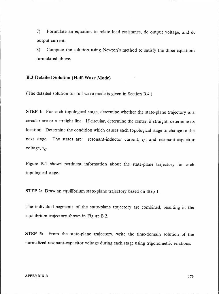
7) Formulate an equation to relate load resistance, dc output voltage, and dc ioutput current.
8) Compute the solution using Newton’s method to satisfy the three equationsformulated above.
B.3 Detailed Solution (Half-Wave Mode) g ‘
(The detailed solution for full-wave mode is given in Section BA.)
STEP 1: For each topological stage, determine whether the state-plane trajectory is acircular arc or a straight line. If circular, determine the center; if straight, determine itslocation. Determine the condition which causes each topological stage to change to thenext stage. The states are: resonant-inductor current, iL, and resonant-capacitor
voltage, vc.
Figure B.1 shows pertinent information about the state-plane trajectory for eachtopological stage.
STEP 2: Draw an equilibrium state-plane trajectory based on Step 1.
The individual segments of the state-plane trajectory are combined, resulting in theequilibrium trajectory shown in Figure B.2.
STEP 3: From the state-plane trajectory, write the time-domain solution of thenormalized resonant-capacitor voltage during each stage using trigonometric relations.
APPENDIX B 170

OE@2
9äé-·
:0n""‘0§
gG
Z
äwZ
¤¤
ef:
U
E
9°~• huZää
I
;»;>
“
.2-
*""']
„
ZG
0ct Z0Z
0Z
3
NT-r·
:-·<
r-Q
EQZ
Tx
E
*-0
"°
<r¤
A
Z,
·—
E90 A r-
.. A :U2
Q
ZZ? :E9
Z *2 ;2
A
‘“„,
¤<
g-• *
—‘L-Ü E
“’—
gg
2%T A-
9 ~T ,
6-
°c:
¤— Z V; : + 9 9*
A8
zu
Z 2 T.:
·6-
¤
6 52 s 2
6 GEQ
-1
3Q
Z,
..1 c__
ca
UU
V U
.-I.:; r·
5_...
cu
VCZ
^<
O:... II
:—·
.i.°>
5:1
°‘· Z5
O
°*°
U6- -
9 Z I.
63
>-
V”* > E
°*’°2%
0
9%
U
*22
0
.¤
Eä
E
5:
6
¢>
ä
O':
°—(9
Q
2
==·°?·
E
Q
‘“
gi?
c>
°··9-::
LO}
U
ää
\*9;
*0F
·¤
E}
‘Is °
dä
[IJ
$0
C50.,
$>
4-:-if!
*—
Ü;Z
I
'
E
gt:
“6
E
;$>‘
-,2
„,_
I
.Q¤
E
55
I
gc:
VJ
-
l"
oo
Q
Q
+8
IV)
~
Ü
·—:
—cc¤>-99
V-*"·*

4l4
STAGE 1: [TO ··· Tl]
STAGE 2: [Tl — T2]
STAGE 3: [T2 — T3] iLN
STAGE 4: [T3 — T4]
V2 [
r Iozv ‘*' [MN2
A”‘^’
. T , T <-—>· T gN 4 · = [ 4;4 4 '| 4• 44 4
4
Figure B.2 Equilibrium state—plane trajectory for the secondary·resonance forwardconverter in half-wave mode.
172

Stage I
VON] = 1 — rl cos(cot — 91) (B — 1)
ATI =
(61Stage2
Stage 3
VCN3 = 1+ F2 COS 94 ’ + ION) (Dt'1
9AT3= -1-rzcos 4 (*8-6)CÜUMN + [011/)
Stage 4
VCNA = “ IMN(D[ "1
+ r cos9AT=T—l-9 6 6 6 4 6-6
STEP 4: Formulate an equation for the dc Voltage gain, VON.
In this converter the output Voltage is the average of the positive portion of the
APPENDIX B 173

resonant—capacitor Voltage. The resonant—capacitor Voltage is positive during Stages 2and 3. The normalized output Voltage (dc Voltage gain) is given by,
_ 1 AT AT
The integrands and the limits of integration in Equation (B-9) have been found in Step3. Making the required substitutions and performing the integration results in,
1 6 2VON rz cos((-)4 + rc/2) + r2 cos
93STEP5: Formulate an equation to describe steady-state conditions.
The value of the normalized resonant—capacitor Voltage at the end of Stage 4 is equal toits value at the beginning of Stage 1.
VCON = ' l’cN4(AT4) (B ‘ 10)
Also, from the state-plane diagram, by trigonometry,
VCON = rl(COS 61) —1
—'Substitutingresults obtained in Step 3 into the right side of Equation (B-10) andsubtracting the right side of Equation (B-11) gives,
N l + rz cos 64f] =0=l—r1(cos91)·—IMN91+92-1-93+94+——cot+————-——2 [MN + [ON
STEP 6: Formulate an equation to describe Volt-second balance on the transformer(which is the same as Volt-second balance on the resonant capacitor in this converter).
APPENDIX B 174

The integral of the (normalized) resonant-capacitor voltage over an entire switchingcycle must be equal to zero.
dz dz = 0 (B - 12)
The sum of the second and third terms of this equation is known from the computationof the dc voltage gain. This gives,
11§‘T¤VON1dV+ TS VON 0 (B — 12)
Substituting for the integrands and the limits of integration, performing the integration,and using the results from the dc voltage gain,
0 = 91+ 92 + 93 + 94 + lg- — r1sin91— r1sin92 + r2cos93 ·— r2cos(94 + rc/2)
(1+ fz cos 94)2 [MN 211: N 1+ r2 cos 94 2hl---- —91—92—93—94———i————
2 (IMN ‘1' low) 2 Fs/Fo 2 [MN J" [01v
STEP 7: Formulate an equation to relate load resistance, dc output voltage, and dcoutput current.
In terms of normalized parameters,
/-0-1/ON-12/z B-2 ‘ " "' 0 ( 14)[ON
STEP 8: Compute the solution using Newton’s method to satisfy the three equationsderived in Steps 5, 6, and 7.
The three equations are:
A1·1>E1~1mx 1; ns

F(X) = fE(X) = O (B ‘ 15)J€(X)
The functionsÄ, Ä, and are defined in the previous three steps. Also, there exist threeunknowns,
Iozv
·
X = [MN (B - 16)
_ Vcozv
Newton’s method is used to iteratively solve these simultaneous nonlinear equations.Newton’s method, and its application in solving this problem, are discussed in Step 9ofAppendix A.
The FORTRAN program written to implement the numerical solution is shown inFigure B.3. A corresponding flowchart is given in Figure B.4. Observe, in the flowchart,that it is necessary for the user to supply an initial guess for the unknown variables. Thisinitial guess must be close enough that Newton’s formula (Equation (A-59)) willconverge. Instead of only calculating results for a single set of input parameters, theprogram generates a "curve" of solutions where a single parameter (normalizedswitching frequency, for example) is swept over a range of values. When this is done,the user need only input the initial guess of the unknowns for the first point to becalculated. After that, the parameter being swept is incremented in sufficiently smallsteps that the results of each previous solution can be used as the initial guess to thesolution of the new point.
APPENDIX B 176

_______________._.____*.......——YwgggXXXXXXXXX—X—————————————————————————————————————————<
C XX SOLVES HALF—NAVE MODE DC CHARACTERISTICS OF THEC XX SECONDARY—RESONANCE FORNARD CONVERTERE XX LEN ROUFBERG AUGUST 20, 1986C INPUTS:C FSFO = FS/FO = NORMALIZED SNITCHING FREQUENCYg ROZO = R/ZO = NORMALIZED LOAD RESISTANCEC ÜUTPUTS :C VON = DC VOLTAGE GAINC IMN = NORMALIZED DC MAGNETIZING CURRENTE VDSPN = NORMALIZED MOSFET PEAK DRAIN—SOURCE VOLTAGEC INTERMEDIATE RESULTS:C ION = NORMALIZED DC OUTPUT CURRENTC VCON = —(NORMALIZED RESONANT-CAPACITOR VOLTAGE ATC THE BEGINNING OF TOPOLOGICAL STAGE 1)CC FUNCTIONS SOLVED BY NENTON'S METHOD:C FSS DESCRIBES STEADY STATE CONDITIONS (=F1)C FVSB DESCRIBES VOLT—SECOND BALANCE (=F2)C FROZO RELATES LOAD RESISTANCE TOC OUTPUT VOLTAGE AND CURRENT (=F3)C
IMPLICIT REALX8 (A—Z)COMMON PIPI=3.14159265
CC XX INPUT INTITIAL PARAMETERS XX
PRINT X,'ENTER ROZO'READ(6,X) ROZOPRINT X,'ENTER FSFO‘
C READ(6,X) FSFOC XX INPUT INITIAL GUESS FOR UNKNONNS XXPRINT X,'ENTER ION'READ(6,X) ION
PRINT X,'ENTER IMN'READ(6,X) IMNPRINT X,‘ENTER VCON'READ(6,X) VCONC
C XX CALCULATE FUNCTION VALUES AT POINT (ION,IMN,VCON) XX10 CALL CALCF(ROZO,FSFO,ION,IMN»VCON,FSS,FVSB,FROZO)A1=FSSA2=FVSBA5=FROZ0
CC XX CHECK IF RESULT NITHIN TOLERANCE XXIF (A1XX2+A2XX2+A3XX2 .LT. 0.00001) GOTO 100CC XX PERTURB ION XX
ION=ION+0.001CALL CALCF(ROZO,FSFO,ION,IMN»VCON,FSS,FVSB,FROZO)A4=FSS
Figure B.3 FORTRAN program to compute the dc characteristics of the secondary-resonance forward converter in half-wave mode.
177

I
I
IA5=FVSBA6=FROZ0
C ION=ION—0.001C XX PERTURB IMN xx
IMN=IMN+0.001CALL CALCF(ROZO,FSFO,ION„IMN„VCON,FSS,FVSB,FROZO)A7=FSSA8=FVSBA9=FROZ0
C IMN=IMN-0.001C XX PERTURB VCON XX
VCON=VCON+0.001CALL CALCF(ROZO,FSFO,ION;IMN,VCON,FSS,FVSB,FROZO)A10=FSSA11=FVSBA12=FROZ0
C VCON=VCON-0.001C xx CALCULATE JACOBIAN xx
J1l=(A4—A1)/0.001J12=(A7—A1)/0.001J13=(A10—A1)/0.001J21=(A5—A2)/0.001J22=(A8—A2)/0.001J23=(A11—A2)/0.001J31=(A6-A5)/0.001J32=(A9—A3)/0.001
C J33=(A12—A5)/0.001C XX CALCULATE INVERSE JACOBIAN (XDET) xx
N11=J22xJ33—J32xJ23N12=J32xJ13—J12xJ33N15=J12XJ23—J22xJ13N21=J23xJ51-J21xJ33N22=J11XJ33-J31xJ13N25=J21xJ15-J11xJ25N31=J21xJ32—J31XJ22N52=J31XJ12—J11xJ32N33=J11XJ22-J21xJ12DET=J11xN1l+J12XN21+J13XN31
CC XX CALCULATE NEN VALUES FOR ION,IMN,VCON Xx
ION=ION—(A1XN1l+A2xN12+A3xN13)/DETIMN=IMN—(AlXN2l+A2XN22+A5XN23)/DETVCON=VCON—(A1XN31+A2XN32+A3XN33)/DETNRITE (6,90)ION„IMN,VCON
90 FORMAT (5E13.4)91 FORMAT (6E13.4)92 FORMAT (2E13.4)
C GOTO 10C xx PRINT RESULTS xx
100 CALL THSRS(ION,IMN,VCON,R1,R2»TH1,TH2,TH5»TH4)
F1gurc B.3 (Contmucd)
178

11
VON=TH5+TH4+PI/2—R2xCOS(TH4+PI/2)VDSPN=VCON+1NRITE (6,110) ROZO,FSFO,ION,IMN,VCON,VON,FSS,FVSBNRITE (8,92) FSFO,VONNRITE (9,92) FSFO,VDSPNNRITE (10,92) FSFO,IMN
C 110 FORMAT (8E13.4)C xx INCREMENT RUNNING PARAMETER xxC FSFO=FSFO+0.01C xx CHECK IF RUNNING PARAMETER EXCEEDS DESIRED RANGE xxIF (FSFO .GT. 1.0 ) STOP
GOTO 10C ENDC xx COMPUTE THETAS (TH1 — TH4) AND RADII (R1,R2) xxE xx (THESE ARE PARAMETERS ON THE STATE PLANE) xx
SUBROUTINE THSRS(ION,IMN,VCON,R1,R2,TH1,TH2,TH5,TH4)IMPLICIT REALx8 (A—Z)COMMON PIR1=SQRT(IMNxx2+(VCON+1)xx2)R2=SORT((SQRT(R1xx2-1)—ION)xx2+1)TH1=ASIN(IMN/R1)TH2=ACOS(1/R1)TH3=ASIN(1/R2) ~TH4=ASIN((IMN+ION)/R2)RETURN
C END xx COMPUTE THE FUNCTIONS: FSS, FVSB, FROZO xxSUBROUTINE CALCF(ROZO, FSFO, ION, IMN, VCON, FSS, FVSB, FROZO)IMPLICIT REALx8 (A—Z)COMMON PICALL THSRS(ION,IMN,VCON,R1,R2,TH1,TH2,TH5,TH4)
CC xx COMPUTE THE STEADY—STATE FUNCTION (FSS) xx
FSS=TH1+TH2+TH3+TH4+PI/2·2xPI/FSFO+(1+R2xCOS(TH4))/(IMN+ION)FSS=—IMNxFSS—R1xCOS(TH1)+1
CC xx COMPUTE THE "VOLT-SECOND BALANCE" FUNCTION (FVSB) xx
FVSB=TH1+TH2+TH5+TH4+PI/2—R1xSIN(TH1)-R1xSIN(TH2)+R2xCOS(TH3)FVSB=FVSB—R2xCOS(TH4+PI/2)+((l+R2xCOS(TH4))xx2)/2/(ION+IMN)0=2xPI/FSFO-TH1—TH2—TH3-TH4—PI/2-(1+R2xCOS(TH4))/(IMN+ION)
C FVSB=FVSB—IMN/2*0**2C xx COMPUTE THE "RO/ZO" FUNCTION (FROZO) xx
v0N=TH3+TH4+PI/2—R2xc0S(TH4+PI/2)VON=(VON+R2xCOS(TH3)+((1+R2xCOS(TH4))xx2)/2/(IMN+ION))xFSFO/2/PIFROZO=VON/ION—ROZORETURN 'END
Figure B.3 (Coritmued)
179
._. _„g__g__________________________._....................................-.--------«

START
INPUT INITIAL PARAMETERSFS/FO, R/ZO
INPUT INITIAL GUESSFOR UNKNOWNS
Ion- [mv- Vcozv I
CALCULATEA-A-A
YES Rßsums wmimTOLERANCE 7
PERTURBCOMPUTE:V [ V [ow- [mv- Vcozv0N• MN• DSPN INDIVIDUALLY, AND RECALCULATEFROM: ION, IHN, VCON
AND·I-' /F R/ZAA'];
° S O° 0 TO DETERMINE JACOBIAN MATRIX
PRINT RI5$UI,T$ INVERT JACOBIAN MATRIX
INCREMENT RUNNING FIND NEW VALUES FORPARAMETER [OM [MM VCON
USING NEWTON'S FORMULA
RUNNING PARAMETEREXCEED DESIRED RANGE 7
YES
DONE
Figure B.4 Flowchart for computing the dc characteristics of the secondary-resonanceforward converter.
180

1B.4 Detailed Solution (Full-WaveMode)The
steps used to determine the dc characteristics in full-wave mode are identical to thatof half—wave mode. However, the state-plane trajectories, equations, and (mostimportant) the results are different.
STEP 1: For each topological stage, determine whether the state-plane trajectory is acircular arc or a straight line. If circular, determine the center; if straight, determine itslocation. Determine the condition which causes each topological stage to change to thenext stage. The states are: resonant-inductor current, iL, and resonant-capacitorvoltage, vC.
Figure B.5 shows pertinent information about the state-plane trajectory for eachtopological stage.
STEP 2: Draw an equilibrium state-plane trajectory based on Step 1.
The individual segments of the state-plane trajectory are combined, resulting in theequilibrium trajectory shown in Figure B.6.
STEP 3: From the state-plane trajectory, write the time-domain solution of thenormalized resonant-capacitor Voltage during each stage using trigonometric relations.
Stage I '
VCN1 = 1 — r1cos(cot — 91) (B — 17)
AT1 = (91 + 92)/co (B — 18)
t— APPENDIX B 181

ä
? ä;EQ 03DZ
° c>cOzi-· " n n E.: 0EF Z 2 2 E *56-$7 F gs ..:> Frgw 6-8 „U ;>- ‘ä
QF EO0 .
F /'\ /'\FU
< z < z E; Q C ::*8gj E er Q 6- ü- 2E
¤>- F 2 6- E S; E < E Q?¤-Ecz Z 6- Z S 6- 7 6 E-¤ ul 0.**NQ zu ,2 Q nu 2. Q ,5 =" Z .,.. 03V- 2 U „ ^ O —-· c> ,.. .,.,.4.
<8 F ~ uu F 2 zu : F LQ 2“
Q‘·>·’“—
Q E 3 3 5 E 2 V 2 Q-:1 Q °»·Q1 0
ZE-· ¤J Lu —· ul bd < Z ct'.—¤ U —¤ - U .2 w 6*-= ; .2;GÖ "J Z 6-]
.E‘Q
5 9 5 8 — u E, *62
‘ wä¢> 322
>„ 03G 0 53::L5}. ° ° Ö) <>° mgE 2 Fw Fw 8* 2%
+> > +> ll OC4-ßa
..:uw; E E"' E 5 V2E-, U- 0
E E 6:. Q 6: Qi,E
uaE Ol Q"} Q5
182

N NN
STAGE 1: [To - TQ]
STAGE 2: [TQ - T3]
STAGE 3: [T3 — T3]
STAGE 4: [T3 — T4}[LNT1
Ä
T2:1
I1
[ ION + [MN
1Q
: ’3 94 II E1 1' T2 N' 1IN·é·*—‘ VCON 1 “"">’ÜI •
· 1I 1:·<———T? Voszw $*-*-*9:
Figure B.6 Equilibrium state·p1ane trajectory for the secondary-resonance forwardconverter in full—wave mode.
183

1Stage
2VCNZ = l + rZ sin(cot — 03) (B — 19)
ATZ = (2 03 + 1:)/co (B — 20)
Stage 3
vc-N3 = l — rg sin(cot + 04) (B — 21)
Stage 4
Vcm = 1 °' V3 $1¤(94 + 96) “ IMNCÜI (B ‘ 23)
AT4=TS°';]$*[91+92+2G3+W+95]STEP
4: Formulate an equation for the dc voltage gain, VON.
The output voltage is the average of the positive portion of the resonant-capacitor
voltage. In full-wave mode, the resonant-capacitor voltage is positive only during Stage
2. The normalized output voltage (dc voltage gain) is given by,
lVON = 7'„;j$T2vCN2 dt (B —— 25)
The integrand and the limit of integration have been found in Step 3. Making the
required substitution and performing the integration gives,
APPENDIX B 184

lIHl
F F (VON rt + 22*2 cos 92] (B —
26)STEP5: Formulate an equation to describe steady-state conditions.
The value of the normalized resonant-capacitor voltage at the end of Stage 4 is equal to
its value at the beginning of Stage 1.
Vcozv = ‘ "c2v4(A724) (B " 27)
Subtracting the right side of Equation (B-27) from the left side and using Equations
(B—23) and (B-24), gives,
fa :0:1—V3SiH(94+95)-IMN[Ä‘*°9l “92"‘293"TE“95]+ VCONFs/Fo
STEP 6: Formulate an equation to describe volt-second balance on the transformer
(which is the same as volt-second balance on the resonant capacitor in this converter).
The integral of the (normalized) resonant-capacitor voltage over an entire switching
cycle must be equal to zero.
j§TlVCNl 42 + jgm VCN2 dr + §$T3VCN3 dz + j§T4VCN4 dr = 0 (ß — 28)
The second term of this equation is known from the computation of the dc voltage gain.
Using Equation (B-25),
jäft VCNI dz dr dz = 0 (B — 29)
|» APPENDIX B l85

lSubstituting for the integrands and the limits of integration, performing the integration,and using the results from the dc Voltage gain,
F95'“r1SiI].91-'rlSiI],62
+ 22*2 cos 95 — r5 cos 94 + 2*5 cos(94 + 95)]
. Fs/F0 22: _ _ 2
STEP 7: Formulate an equation to relate load resistance, dc output Voltage, and dcoutput current.
ln terms of normalized parameters,
f—0—V°^’—R/Z 12-303 ‘ " T" 0 ( )ON
STEP 8: Compute the solution using Newton’s method to satisfy the three equationsderived in Steps 5, 6, and 7.
The description of Newton’s method is given in the corresponding step for half-wavemode (Section B.3, Step 8). The flowchart for the numerical solution of the equationsis also the same as for half-wave mode, shown in Figure B.4. The only differencesbetween the programs for half-wave and full-wave mode are the functions, jj, ß, and J5,and some of the intermediate variables. The FORTRAN program written to implementthe numerical solution, for full-wave mode, is shown in Figure B.7.
APPENDIX B 186

SS
SC XX SOLVES FULL—WAVE MODE DC CHARACTERISTICS OF THEC XX SECONDARY-RESONANCE FORWARD CONVERTERE XX LEW ROUFBERG AUGUST 21, 1986C INPUTS:C FSFO = FS/FO = NORMALIZED SWITCHING FREQUENCYE ROZO = R/ZO = NORMALIZED LOAD RESISTANCEC UUTPUTS:C VON = DC VOLTAGE GAINC IMN = NORMALIZED DC MAGNETIZING CURRENTVDSPN = NORMALIZED MOSFET PEAK DRAIN—SOURCE VOLTAGEC INTERMEDIATE RESULTS:C ION = NORMALIZED DC OUTPUT CURRENTC VCON = -(NORMALIZED RESONANT—CAPACITOR VOLTAGE ATE THE BEGINNING OF TOPOLOGICAL STAGE 1)C FUNCTIONS SOLVED BY NEWTON'S METHOD:C FSS DESCRIBES STEADY STATE CONDITIONS (=F1)C FVSB DESCRIBES VOLT—SECOND BALANCE (=F2)C FROZO RELATES LOAD RESISTANCE TOC OUTPUT VOLTAGE AND CURRENT (=F3)C
IMPLICIT REALX8 (A—Z)COMMON PIPI=3.14159265
CC XX INPUT INTITIAL PARAMETERS XX
PRINT X,'ENTER ROZO'READ(6,X) ROZOPRINT X,'ENTER FSFO'READ(6,X) FSFO
CC XX INPUT INITIAL GUESS FOR UNKNOWNS XX
PRINT X,'ENTER ION'READ(6,X) IONPRINT X,'ENTER IMN'READ(6,X) IMNPRINT X,'ENTER VCON'READ(6,X) VCON
CC XX CALCULATE FUNCTION VALUES AT POINT (ION,IMN,VCON) XX
10 CALL CALCF(ROZ0,FSFO,ION»IMN,VCON,FSS,FVSB,FROZO)A1=FSSA2=FVSB
C A5=FROZ0C XX CHECK IF RESULT WITHIN TOLERANCE XX· IF (A1XX2+A2XX2+A3XX2 .LT. 0.00001) GOTO 100CC XX PERTURB ION XX
ION=ION+0.001CALL CALCF(ROZ0,FSFO,ION,IMN,VCON,FSS,FVSB,FROZO)A4=FSS
Figure B.7 FORTRAN program to compute the dc characteristics of the secor1dary·ICSOIIZIHCC H1 mOdC.
187

A5=FVSBA6=FROZ0
C ION=ION-0.001C XX PERTURB IMN XX
IMN=IMN+0.001CALL CALCF(ROZO,FSFO,ION,IMN,VCON,FSS,FVSB,FROZO)A7=FSSA8=FVSBA9=FROZ0
C IMN=IMN—0.001C XX PERTURB VCON XX
VCON=VCON+0.001CALL CALCF(ROZO„FSFO,ION,IMN»VCON,FSS,FVSB,FROZO)A10=FSSA11=FVSB, A12=FROZ0
C VCON=VCON—0.001C xx CALCULATE JACOBIAN xx
J11=(A4'Ä1)/Ü.ÜÜ1J12=(A7—A1)/0.001J13=(A10—A1)/0.001J21=(A5—A2)/0.001J22=(A8—A2)/0.001J25=(A11-A2)/0.001J31=(A6—A3)/0.001J32=(A9—A5)/0.001J33=(A12-A3)/0.001C
C XX CALCULATE INVERSE JACOBIAN (xDET) xxN11=J22XJ33-J52xJ23N12=J32xJ15-J12xJ33N13=J12xJ25-J22xJ13N21=J23xJ51—J21xJ35N22=J11xJ35-J31xJ15
I N23=J21xJ13-J11xJ25N31=J2lxJ32—J31xJ22N32=J31XJ12—J11xJ32N33=J11xJ22—J21xJ12
C DET=J11XN11+J12xN21+J13xN31C XX CALCULATE NEN VALUES FOR ION,IMN,VCON xx
NRITE (6„90)ION,IMN„VCON90 FORMAT (5E13.4)91 FORMAT (6E15.4)92 FORMAT (2E15.4)C GOTO 10C xx PRINT RESULTS xx100 CALL THSRS(ION,IMN,VCON,R1,R2,R3•TH1,TH2»TH3,TH4,TH5)
Figure B.7 (Contmued)
188

v0N=(2XTH3+PI+2XR2Xc0S(TH3))XFSF0/2/PIVDSPN=VCON+1NRITE (6,110) ROZO,FSFO,ION,IMN,VCON,VON,FSS,FVSBNRITE (8,92) FSFO,VONNRITE (9,92) FSFO,VDSPNNRITE (10,92) FSFO,IMN
C 110 FORMAT (8E13.4)C XX INCREMENT RUNNING PARAMETER XXC FSFO=FSFO+0.01C XX CHECK IF RUNNING PARAMETER EXCEEDS DESIRED RANGE XX
IF (FSFO .GT. 1.0 ) STOPGOTO 10
C ENDC XX COMPUTE THETAS (TH1 - TH4) AND RADII (R1,R2) XX_ E XX (THESE ARE PARAMETERS ON THE STATE PLANE) XX
I SUBROUTINE THSRS(ION,IMN,VCON,R1,R2,R3,TH1,TH2,TH3,TH4,TH5)IMPLICIT REALX8 (A—Z)COMMON PIR1=SQRT(IMNXX2+(VCON+1)XX2)R2=SQRT((SQRT(R1XX2—1)—ION)XX2+1)R5=SQRT((SQRT(R2XX2-1)—I0N)XX2+1)TH1=ASIN(IMN/R1)TH2=ACOS(1/R1)TH3=ASIN(1/R2)TH4=ASIN(1/R3)TH5=PI/2-TH4—ASIN(IMN/R3)RETURN
C ENDC XX COMPUTE THE FUNCTIONS: FSS, FVSB, FROZO XXC
SUBROUTINE CALCF(ROZ0, FSFO, ION, IMN, VCON, FSS, FVSB, FROZO)IMPLICIT REALX8 (A—Z)COMMON PICALL THSRS(ION,IMN,VCON,R1,R2,R3,TH1,TH2,TH3,TH4,TH5)
CC XX COMPUTE THE STEADY-STATE FUNCTION (FSS) XX
FSS=IMNX(2XPI/FSFO—TH1—TH2-2XTH3-PI—TH5)FSS=1—R3XSIN(TH4+TH5)—FSS+VCON
CC XX COMPUTE THE "VOLT-SECOND BALANCE" FUNCTION (FVSB) XX
FVSB1=(2XTH3+P1+2XR2XCOS(TH3))XFSFO/2/PIFVSB2=(TH1+TH2-R1XSIN(TH2)—R1XSIN(TH1))XFSFO/2/PIFVSB3=(TH5+R3XCOS(TH4+TH5)—R5XCOS(TH4))XFSFO/2/PIFVSB4=(1—R3XSIN(TH4+TH5))X(1—(TH1+TH2+2XTH3+PI+TH5)XFSFO/2/PI)FVSB5=IMNX((2XPI/FSFO—TH1—TH2—2XTH3-PI—TH5)XX2)XFSFO/4/PIFVSB=FVSB1+FVSB2+FVSB3+FVSB4—FVSB5
CC XX COMPUTE THE "R/ZO" FUNCTION (FROZO) XX
VON=(2XTH3+PI+2XR2XCOS(TH5))XFSFO/2/PIFROZO=VON/ION-ROZ0RETURNEND
Figure B.7 (Continued)
189
_w(YY_________„„„_________.„................„........................................J