Embed Size (px)
Citation preview

Convergent beam electron diffraction
P. E. CHAMPNESS
Department of Geology, University of Manchester, Manchester M13 9PL
Abstract
In convergent-beam electron diffraction (CBED) a highly convergent electron beam is focussed on to a small (~< 50 nm) area of the sample. Instead of the diffraction spots that are obtained in the back focal plane of the objective lens with parallel illumination in conventional selected-area electron diffraction, CBED produces discs of intensity. The point group can be determined uniquely from the symmetry within the individual discs and the overall pattern. In order to determine the point group, it is usually necessary to record a number of CBED patterns with the electron beam aligned along different zone axes, but sometimes only one, high-symmetry pattern is required. The positions of reflections in higher-order Laue zones can be used to identify the crystal system and lattice type and to detect the presence of certain glide planes. The repeat along the zone axis that is parallel to the beam c~n be calculated from the diameters of the Laue zones. Hence the presence ofpolymorphs can be detected. Doubly-diffracted discs in CBED often contain a 'line of dynamic absence', the orientation of this line with respect to the symmetry seen in the bright field disc allows the symmetry element responsible for it (glide plane or screw diad) to be identified. This allows 191 of the 230 space groups to be uniquely identified. The measurement of specimen thickness, extinction distance and ceil parameters are also briefly discussed.
K E Y WORD S: convergent beam electron diffraction, electron microscopy, electron diffraction.
Introduction
CONVERGENT beam electron diffraction (CBED) was first described in 1939 by Kossel and M611en- stedt. However, it was not until the advent of transmission electron microscopes with STEM (scanning-transmission electron microscope) pole pieces and 'clean' vacuum systems in the 1970s that the technique became more widely used in materials science. Its use in mineralogy so far has been minimal, although in 1975 Goodman used CBED to show that the space group of 2M biotite was C2 and not C2/c, as had been previously assumed. In 1977 Goodman and Johnson also indicated how the technique could be used to distinguish between enantiomorphous space groups and specifically those of quartz. In this paper I will describe in some detail how CBED can be used to determine the point group and space group of a crystalline material and how the polytype of a member of a polytypic series can be determined from a CBED pattern taken with the electron beam perpendicular to the layers. Other applications of CBED patterns will also be mentioned.
i For CBED large illumination angles are required. This results in a disc of confusion due to spherical aberration (Cliff and Kenway, 1982). Thus, although a
Mineralogical Magazine, March 1987, Vol. 51, pp. 33-48 Copyright the Mineralogical Society
Instrumental and specimen conditions for CBED
In conventional, selected-area electron-diffrac- tion a parallel beam is used to illuminate the specimen and the diffraction pattern that is formed in the back focal plane consists of sharp spots (Fig. 1 a). In this method the region of interest is selected by inserting an aperture in the first image plane of the objective lens (the selected-area aperture). Be- cause of the inherent spherical aberration of the objective lens, a slightly different area is selected for each diffracted beam, the error increasing with the diffracting vector g. Thus the smallest area that can be selected in this way is limited to ~ 0'5 pm at 100 kV.
When a focussed, convergent beam illuminates the specimen the diffraction pattern consists of discs, the diameters of which depend upon the convergent angle 2~ (Fig. ib). The area from which the diffraction information comes is (neglecting beam broadening in the specimen) that illuminated by the electron beam. In modern TEMs the spatial resolution for CBED is about 50-100 nm 1. Clearly one application of CBED is in the acquisition of
probe may have a nominal size of 2 nm, the disc of confusion, and hence the area from which a CBED pattern is obtained, is typically 50-100 nm.

34 P . E . C H A M P N E S S
A' BV VB' Thin specimen
Section
/ �9 - @ 0 @ Diffracted spot Z~ro order spot Diffracte~d disc Ze~ro order disc
(~ (b) FIG. 1. The formation of (a) a conventional (selected-area) electron diffraction pattern and (b) a convergent-beam electron diffraction (CBED) pattern. In (a) the area AA' is selected by means of an aperture in the first image plane of the objective lens (not shown), whereas in (b) the area, BB', selected is determined by the probe size. The diameter of the discs
in the CBED pattern depends upon the convergence angle, 2ct.
conventional diffraction information (lattice type, crystal system, interplanar spacings and angles) from very small areas. When used in this way the technique is often known as 'microdiffraction' (Steeds, 1981).
If the specimen is very thin, kinematic conditions prevail and the discs show uniform contrast 1 (Fig. 2a). In thicker samples dynamical interactions become important. Provided that the area of the specimen selected by the beam is undeformed, contrast appears in the discs (Fig. 2b). It is from this dynamical contrast that point-group and space- group information is derived.
In order to ensure that the area from which the C B E D pattern comes is undeformed, the nominal probe size should generally be ~< 40 nm. Such probe sizes require a highly convergent objective- lens system; TEMs fitted with STEM pole pieces
i The limit for purely kinematic scattering is around 10% of the shortest (many-beam) extinction distance, {g, on a particular zone axis. (R. Vincent, pers. comm.). In a typical silicate the shortest (g would be about 50/am.
provide the probe sizes and convergence angles required.
Other important instrumental requirements for the full exploitation of the information available from CBED are: a range of camera lengths from about 250 to about 1000 mm, a field of view of at least 15 ~ in the diffraction plane, a eucentric, high-angle tilting stage 2 and a high vacuum with a very low partial-pressure of hydrocarbons. When this latter requirement is not met, contamination spots form rapidly where the electron beam is focussed on the specimen and the dynamical detail in the CB pattern is obliterated. Steeds (1979) describes ways of minimising the contamination rate.
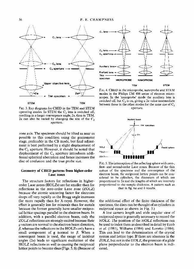
Fig. 3 shows the experimental conditions for acquiring a convergent beam in the T E M and STEM modes. When the instrument is operated in the STEM mode, the second condenser lens is
z However Eades et al. (1983) urge caution in inter- preting CBED patterns from specimens tilted by more than 40 ~ .

C O N V E R G E N T BEAM E L E C T R O N D I F F R A C T I O N
l :g C
35
FIG. 2. (a) [100] 'microdiffraction' pattern from olivine, space group Pbnm. The specimen is sufficiently thin that reflections 00l are genuinely absent for I = 2n + 1. They are forbidden by both the n glide parallel to (010) and the screw diad parallel to z. Note that all reflections for which k = 2n + 1 are absent in this section due to the b-glide parallel to (100). (b) [100] CBED pattern from a thicker area of the same sample showing 'zero-order' detail in the discs. Note that
the 'forbidden' reflections 001, l = 2n + 1 are present, but contain lines of dynamic absence.
switched off. The convergence angle in STEM is typically about four times larger than that obtained in the TEM mode for the same C2 aperture. The Philips EM 400 series of electron microscopes has a very useful TEM mode known as the 'nanoprobe mode' (Fig. 4) in which, in contrast to the 'micro- probe' mode, the auxiliary lens is switched off. This results in a range of convergence angles intermediate between the 'microprobe' and STEM modes, and nominal probe sizes down to ~ 5 nm.
It is apparent from Figs. 3 and 4 that the convergence angle is varied, not only by the second condenser and objective lens configuration, but also by the size of the C 2 aperture. For most applications it is desirable that the diffraction discs do not overlap: ideally they should just touch. A range of C2 aperture sizes is therefore needed if specimens with different cell parameters are to be studied in a variety of crystallographic orienta- tions.
The spot size in CBED is a function of the operational mode (TEM [microprobe or nano-
probe], STEM) and of the excitation of the C1 lens, with appropriate adjustment of the C2 lens. For further details of experimental procedures, the reader is referred to Williams (1984), Chapter 6 or Steeds (1979, 1981).
Steeds (1979) describes in detail the adjustments that need to be made to the electron microscope in both TEM and STEM modes in order to ensure the desired quality of the CBED pattern. Only the two most important adjustments will be described here. Firstly one must ensure that the beam is accurately focussed on the specimen. This is most easily done by moving the spot to an edge or other prominent feature. At exact focus, no spatial information will be present in the CB discs. The presence of a shadow image in the discs indicates the need to adjust the objective (in STEM mode) or second condenser (in TEM) lens. Focus is at the point of inversion of the shadow image (see Steeds, 1979, Fig. 15.4).
For most of the applications described in this paper, the electron beam must be exactly along a
36 P. E. C H A M P N E S S
~- -- C1 lens ~ ~
~ - - ~- ~""~ /
, ~ L _ _ _ _ <___~ =C p';r;~re ='~ _ 4 \
/Upper objective lens < ~ .
2Q, ~ - Thin specimen
STEM TEM
FIG. 3. Ray diagrams for CBED in the TEM and STEM operating modes. In STEM the C 2 lens is switched off, resulting in a larger convergence angle, 2c~, than in TEM. 2c~ can also be varied by changing the size of the C 2
aperture.
zone axis. The specimen should be tilted as near as possible to this condition using the goniometer stage, preferably in the CB mode, but final adjust- ment is best performed by a slight displacement of the C2 aperture. However, it should be noted that displacement of the C z aperture introduces addi- tional spherical aberration and hence increases the disc of confusion and the true probe size.
Geometry of CBED patterns from higher-order Laue zones
The structure factors for reflections in higher- order Laue zones (HOLZs) are far smaller than for reflections in the zero-order Laue zone (ZOLZ) because the atomic scattering factor for electrons drops off very rapidly as the Bragg angle increases (far more rapidly than for X-rays). However, the effect is generally less for minerals than for metals because the former generally have smaller recipro- cal lattice spacings parallel to the electron beam. In addition, with a parallel electron beam, only the Z O L Z reflections are strongly excited because their 9 vectors are normal to the electron beam direction, /~, whereas the reflections in the HOLZs only have a small component of g normal to /L When a convergent beam is used, the range of incident angles (2~) leads to significant excitation of the H O L Z reflections as well as causing the reciprocal lattice points to become discs (Figs. 5, 6). (Because of
C, lens ~, ~ ~
C= lens ~ < ~ ~ . ~ /
C= aper ture~ ~
specimen MICROPROBE
TEM
r
NANOPROSE
STEM
FIG. 4. CBED in the microprobe, nanoprobe and STEM modes in the Philips EM 400 series of electron micro- scopes. In the 'nanoprobe' mode the auxiliary lens is switched off, but C 2 is on, giving a 2a value intermediate between those in the other modes for the same size of Cz
aperture.
Incident beam Thin specimen
A,~ 2cJr
wald sphere
FIG. 5. The interception of the reflecting sphere with zero-, first- and second-order Laue zones. Because of the thin nature of the specimen and the convergence of the electron beam, the reciprocal lattice points can be con- sidered to be cylinders, the diameters of which are proportional to 2c~ and the lengths of which are inversely proportional to the sample thickness. A pattern such as
that in fig. 6a and b results.
the additional effect of the finite thickness of the specimen, the discs can be thought of as cylinders in reciprocal space as shown in Fig. 5.)
A low camera length and wide angular view of reciprocal space is generally necessary to record the HOLZ. The position of the H O L Z reflections can be used to index them as described in detail by Ecob et al. (1981), Williams (1984) and Loretto (1984). This can lead to the determination of the crystal system and lattice type. If there are absences in the ZOLZ, but not in the HOLZ, the presence of a glide plane perpendicular to the electron beam is indi- cated.

CONVERGENT BEAM ELECTRON DIFFRACTION 37
C* I
ooooo' ooo o,~)o o
o o I o o o I o
o o o I o
o o o / o o o o o o o o 0 o o 0 8 0 o oooo~Doo o o , o o ooooo~oooo oo 0 ~ 0 a* 0 O 0 0 0 0 ~@G'~B'G'O .......... "<9 .... "~ 0 0
oooooooooo o
o ooooooo o o o %o o 0 o ~
o o o o o o o o
~176176176176 00080 b o ooo
FIG. 6. (a) [010] 'microdiffraction' pattern of MgGeO 3 clinopyroxene taken at a camera length of 290 mm with a divergence angle of 1.4 x 10- 3 radians, 120 kV. Individual reflections can be seen in the zero- and first-order Laue zones. (b) Diagram of the pattern in (a). The extension of c* into the FOLZ shows that the FOLZ reflections are displaced by
a*/2 with respect to the ZOLZ.
Fig. 4a shows a CBED pattern taken at low camera length along [010] of a synthetic mag- nesium germanate. This phase was detected in samples of MgzGeO 4 composition synthesised at high pressure, but selected-area diffraction patterns did not fit the olivine, spinel or #-phase structures. Quantitative X-ray microanalysis was impossible due to the overlap of the Mg-K and Ge-L peaks in the energy-dispersive spectrum, although it did suggest that the Mg:Fe ratio was considerably lower in the phase than in the bulk starting material.
Tilting experiments in reciprocal space suggested that the lattice was C-face centred monoclinic. The microdiffraction pattern in Fig. 6a was taken with the electron beam travelling along the direction which was thought to be the unique axis [010]. FOLZ reflections are clearly visible. Careful study of their relationship with the ZOLZ, as shown in Fig. 6b shows that the FOLZ stacks vertically above the ZOLZ, except that it is displaced by a*/2. This confirms that the unit cell is monoelinic and C-face centred (in the ZOLZ, for reflections hOl, h = 2n; in the FOLZ, for reflections hll, h = 2n+ 1). The doubled spacing along c* in the FOLZ results from a c-glide plane parallel to (010) (for reflections hOl, l = 2n; for reflections hll, there are no ab- sences). Hence the space group is either C2/c or Cc. We will see in the next section that the symmetry of the dynamical information in convergent beam patterns taken along [010] allows these two space groups to be distinguished.
Symmetry of CBED patterns
Because of the strong dynamical scattering of electrons by crystals Friedel's law, (which states that the intensity of the reflection hkl is equal to the intensity of hkl, whether the crystal contains a centre of symmetry or not) fails and the 32 crystal point groups are not reduced to the 11 Laue groups as occurs for X-ray and neutron diffraction, except under 'anomalous' scattering conditions. The CBED patterns contain three-dimensional crystal- lographic information, despite being viewed and recorded in two dimensions. The symmetry of a CBED pattern that has been recorded with the electron beam travelling exactly along a zone axis belongs to one of 31 diffraction groups that are isomorphic with the crystallographic point groups of two-dimensional plane figures (the Shubnikov groups of coloured, plane figures) (Buxton et al., 1976). The symmetry elements of the point group that are 'seen' by the electron beam, and thus determine the diffraction group for the zone axis, are those that leave the beam direction, but not necessarily its sense, unchanged (Eades et al., 1983). These are 1, the vertical symmetry elements 2, 3, 3, 4, 4, 6, 6, m and the horizontal symmetry elements 2, ], 4, 7~, 6, 6, m. The relationship between the diffraction groups and crystal point groups is shown in Table 1 which is taken from Buxton et al. (1976). It is not necessary, for the purposes of this paper, to explain the symbols used by Buxton et al. for the diffraction groups.

38 P . E . C H A M P N E S S
FIG. 7. CBED patterns taken at different camera lengths and divergence angles along (100) of gahnite, ZnAl204, spinel, 120 kV. (a) Pattern taken at a camera length of 1150 mm and divergence angle of 4.9 x 10- 3 radians. Diffuse, zero-order information is visible in all reflections and sharp HOLZ lines are visible in the bright-field, 000, spot. The line that arises from the 21,7,1 reflection in the FOLZ is indicated. (b) Pattern taken at a camera length of 210 ram, 2ct = 2.3 x 10 .3 radians. The 21,7,1 excess HOLZ line that is parallel to the defect HOLZ line indicated in (a) is arrowed. (c) Pattern taken at a camera length of 210 mm, 2c~ = 16.2 x 10 - 3 radians. Because the FOLZ reflections overlap, the excess HOLZ lines form a continuous ring that clearly outlines the FOLZ (labelled 1). HOLZ Kikuchi lines are also clearly visible in
the pattern as is the second-order Laue zone (labelled 2). The third-order Laue zone (labelled 3) is faint.
The detail seen in CBED patterns is of two basic kinds; diffuse I scattering within the discs (Fig. 2b, 7a, 8a) and sharp lines which are visible both within the discs and outside them (Fig. 7, 8). The diffuse contrast arises from dynamic interactions within the zero layer (I will henceforth call it zero-order information). Because it is often associated with quite short extinction distances, it is sensitive to thickness and can, in favourable circumstances, be used to determine the thickness of the specimen (see later). The symmetry of the zero-order information in a zone axis pattern (ZAP) is the projected, two-dimensional symmetry of the crystal along the zone axis and belongs to one of the ten two- dimensional point groups (Table 2).
The sharp lines within the discs arise from three-dimensional diffraction. They are equivalent to Kossel lines in X-ray diffraction and are the result of elastic scattering by the planes in higher- order Laue zones (HOLZs). These ' H O L Z lines' are sensitive to very small changes in lattice parameters (and can, in principle, be used to measure the latter) and are thus degraded by small lattice strains. The H O L Z lines occur in pairs (like Kikuchi lines) with a bright (excess) line associated with the H O L Z disc responsible for it (Fig. 7b) and a parallel, dark line present in the bright field disc
1 This diffuse scattering arises from amplitude addition of zero-layer Bloch states and should not be confused with diffuse scattering that occurs outside the reciprocal lattice points and arises from disorder in the crystal.
(Fig. 7a). (The pair of lines indicated in Figs 7a and b are the result of scattering from the (21, 7, 1) plane.)
The sharp lines outside the discs are the result of inelastic scattering from the H O L Z planes. They are analogous to the Kikuchi lines that arise from Z O L Z planes in both conventional, selected-area electron diffraction and in C B E D and are known as ' H O L Z Kikuchi lines'. H O L Z Kikuchi lines are continuous with the H O L Z lines within the discs, but are generally less sharp (Steeds, 1979).
Because extinction distances for H O L Z reflec- tions are long, thick crystals are needed if sharp H O L Z lines are to be obtained. Although the crystal in Fig. 2b was thick enough to show zero-order (diffuse) information in the CBED pattern, it was not thick enough for H O L Z lines or H O L Z Kikuchi lines to be produced. In contrast, H O L Z Kikuchi lines, together with (ZOLZ) Kikuchi lines and excess H O L Z lines can be clearly seen in Figs. 7c and 8b. Figs. 7c and 8b were taken at a short camera length and with a moderate to large convergence angle, 2~, the best conditions for observing these features.
Steeds (1979, 1981) discusses the visibility of H O L Z lines at some length. In minerals they are usually easy to produce because of the large cell dimensions involved and the relative (compared with many metals) perfection of minerals. I have not found the amorphous layer produced at the surface of the specimen by ion-beam thinning to be the problem that Steeds (1981) suggests it can be.
As the H O L Z detail in the CBED patterns is

C O N V E R G E N T BEAM E L E C T R O N D I F F R A C T I O N 39
FIG. 8. [010] CBED patterns of clinopyroxene MgGeO 3 taken at two different camera lengths. (a) Pattern taken at long camera length (1150 mm) showing that the bright field and zero-order symmetries are both 2. (b) Pattern taken at a camera length of 290 mm and the same 2~ value as in (a). The symmetry of the fine lines shows that the whole-pattern symmetry is 2. The excess HOLZ lines define the higher-order Laue zones. The first-, second-, and third-order Laue
zones are labelled 1, 2, 3 respectively. Measurement of the diameter of the FOLZ gave b ~ 9.2 ~.
associated with very long extinction distances, typically several microns, it is relatively insensitive to variations in thickness. Zone axis patterns (ZAPs) from high-symmetry directions can there- fore be used to aid the identification of phases. An atlas of CBED patterns from common alloy phases has recently been published (Steeds et al., 1984).
I will describe below how the possible diffraction group of a ZAP may be found from the zero-order (ZO) symmetry, the 'whole pattern' (WP) symmetry (that shown by the H O L Z lines and the H O L Z Kikuchi lines) and the 'bright field' (BF) symmetry (the symmetry of the H O L Z lines in the bright-field, 000, disc), as described by Loret to (1984) and shown in Table 2. Possible point groups are then deter- mined from Table 1. In favourable cases, only one set of ZAPS, taken along a direction of high symmetry, is necessary to determine the point group. Steeds and Vincent (1983) and Steeds (1984) describe the sequence of steps that are necessary to locate high-symmetry zone axes.
The internal symmetry of dark-field reflections when they are tilted to the exact Bragg condition may also be used to determine the possible diffrac- tion group as described by Buxton et al. (1976) and Steeds (1979, 1984). However, although the addi- tional use of dark-field symmetry will uniquely determine the diffraction group for a ZAP, whereas use of ZO, WP and BF information alone may not, it is often easier and quicker to tilt to another zone axis, or to use other available information
about the sample in order to determine its point group.
Some examples The use of Tables 1 and 2 to determine the point
group is best illustrated by examples. Figs. 8a and b show CBED patterns taken
exactly along [010] of the magnesium germanate phase discussed earlier. Fig. 8a was recorded at a camera length of 1150 mm. A moderate 2~ was used in order to show the symmetry of the dynamical information within the Z O L Z reflections. Fig. 8b, on the other hand, was taken at a camera length of 290 mm, but with the same 2~ value as in Fig. 8a, in order to reveal the whole-pattern symmetry. The patterns that show ZO -- BF = WP = 2 and, from Table 2, the diffraction group is either 2 or 21R. Table 1 shows that these symmetries are consistent with point groups 2/m or 2, but not m. As we saw from the last section that the space group is either C2/c or Cc, the C B E D patterns in fig. 8 show that the space group is C2/e.
Unit cell dimensions were found by electron diffraction to be a ~ 9 . 6 , b ~ 9 . 2 , e ~ 5 . 2 / ~ , /~ = 101 ~ The phase was identified as MgGeO3 clinopyroxene, which Ozima and Akimoto (1983) found from X-ray diffraction to have a = 9.6010, b = 8.9323, c = 5.1592/~, /~ = 101.034 ~ space group C2/c. Note that all the information about the unit cell and space group of the phase could have been determined from conventional, selected-area

40 P . E . CHAMPNESS
TABLE 1. Relation between the diffraction 9roups and the crystal point groups (after Buxton et al., 1976; reproduced by permission of the Royal Society)
and convergent-beam diffraction patterns taken along a single axis, [010] (the b repeat could have been determined from the radius of the FOLZ ring, as described in the next section).
The (100) patterns from gahnite spinel in fig. 7 clearly show that ZO = BF = WP = 4mm. According to Table 2 the diffraction group is either 4ram or 4mml n and Table 1 shows that these symmetries are consistent with the tetragonal point groups 4/mmm and 4ram and the cubic point group m3m. Confirmation of the cubic point group could be made either by recording patterns along another zone axis or by measurement of the diameter of the FOLZ (see next section).
Fig. 9 shows CBED patterns of nigerite, a Sn, Zn, A1 oxide that is related to gahnite spinel and occurs in a number of polysomatic forms (Bannister et aL, 1947; Grey and Gatehouse, 1979). Figs. a-c were all taken along the same high-symmetry direction. In Fig. 9 the zero-order symmetry is 6ram while the BF disc in Fig. 9b and the whole pattern in fig. 9c both show 3m symmetry. Reference to Table 2 shows that the diffraction group is 6Rmma and, from Tables 1 and 3, the patterns are either from F001] in point group ~m or from (111) in point group m3m.
Tilting the specimen by approximately 20 ~ about the perpendicular to a mirror plane in the BF disc produced a zone axis for which ZO = 2ram, BF =

C O N V E R G E N T B E A M E L E C T R O N D I F F R A C T I O N 41
FIG. 9. CBED patterns from the 6H polysome of nigerite. (a) [001] pattern at moderate camera length and convergence angle showing that the whole-pattern symmetry (sharp lines) is 3m while the zero-order (or projection) symmetry (diffuse scattering within the discs) is 6mm. (b) The-bright field disc from a [001] pattern taken at a higher convergence angle than (a), showing that the bright-field symmetry is 3m. (c) [001] pattern taken at low camera length with the same convergence angle as (a), but at a longer exposure, showing a whole-pattern symmetry of 3m. Measurement of the bright HOLZ ring (arrowed) gave c ~ 13.6/~, showing that the polysome is 6H. However, the presence of three faint HOLZ rings inside the bright one indicates that the 24H polysome is also present. (d) Pattern taken with the electron beam parallel to a zone axis at ~ 20 ~ from [001]. The zero-order symmetry is 2ram and the bright-field and whole-pattern
symmetries are 2.

SOLZ
FOLZ
ZOLZ
42 P. E. CHAMPNESS
j r e
FIG. 10. The information needed to determine the spacing between reciprocal lattice planes parallel to the electron beam. Reproduced from Williams (1984) with the permis-
sion of Philips Electronic Instruments, Inc.
WP = m (Fig. 9d). From Table 2 the diffraction group is 2RmmR. Although this diffraction group is consistent with a <UOW> zone axis for 3m or <UV0> for m3m (Tables 1 and 3), no <UV0> zone axis lies at 20 ~ from <I 11>, rotated about <110> in the cubic system. Thus the point group must be 3m, as found by Bannister et al. (1947) for the 6-layer stacking variant of nigerite. We will see in the next section that this result could have been derived directly from Fig. 9a by measurement of the FOLZ ring.
The two examples cited above underline the importance of locating high-symmetry (low-index), zone directions for CBED experiments. As is apparent from Table 1, the higher the symmetry of the diffraction group, and hence the zone axis from which it comes (i.e. the higher its position in the table), the smaller is the number of possible point groups.
The reader may be wondering how sensitive CBED is in detecting small deviations from exact point group symmetry. Ecob et al. (1981) described a technique for computer simulation of HOLZ lines in the BF disc. They used the method to simulate small, tetragonal deviations from cubic symmetry in < 111 > CBED patterns from nickel-based alloys. They showed that the smallest value of the degree of tetragonality, expressed as ( c - a)/(c + a), that could be detected in the simulations was approximately 7 x 10 -s, corresponding to c/a = 1.00014. Ecob et al. pointed out, however, that it is the quality of the experimental pattern that limits the overall pre- cision and they discussed at length the effects that give rise to these limitations. In a companion paper Porter et al. (1981) detected a tetragonality of c/a = 1.0025 in experimental < 111 > patterns.
P. R. Buseck and co-workers have attempted to use CBED to detect the reduction from cubic symmetry in granditic garnets that manifests itself
Table 2. Table showing the relationship between the observed symmetries in convergent beam diffraction patterns and the 31 diffraction groups. (Modified from Loretto, 1984.)
Zero order
(2D symmetry)
Symmetry of high-order (3D) information Possible Diffraction
Whole pattern Bright field Groups
1 1 1 1
1 2 1 R
2 2 2 2 o r 21 R 1 I 2 R
m 1 m m R m m m
m 2 ~ m l R
2mm 2 2v~ 2mRm R 2ram 2ram 2ram o r 2nnal R
m m 2 RmmR
3 3 3 3 3 6 31B
3m 3 3m 3m R 3m 3m 3m 3m 6mm 3ml R
4 4 4 4 or 41R 2 4 4 R
4~ 4 4ram 4mRm R 4ram 4mm 4~ or 4mml R 2mm 4mm 4Rmm R
6 6 6 6 or 61R 3 3 6 R
6mm 6 6mm 6mRm R 6ram 6tram 6rmm or 6mml R 3m 3m 6Rmm R

CONVERGENT BEAM ELECTRON DIFFRACTION 43
Table 3. The d i f f r a c t i o n group symmetry seen in convergent beam d i f f r a c t i o n p a t t e r n s from d i f f e r e n t zone axes ( a f t e r Buxton et a l . 1976, reproduced by permiss ion of the Royal Soc ie t y ) .
po in t group (11 ; ) (100/ (110) <uvo> <uuw> <uvw>
m3m 6Rmm R 4mml R 2mm]R 2Rmm R 2Rmm R 2 R 43m 3m 4Rmm R ml R m R m I 432 3m R 4mRm R 2mRm R m R m R 1
point group (Ill> <I00> luvo) (uvw>
m3 6 R 2mml R 2Rmm g 2 R 23 3 2mRm R m R I
po in t group [001] (100) <ITO) <uvo> (uuw) /uuw) (uvw)
6/mmm 6mml R 2mml R 2mml R 2Rmm R 2Rmm R 2Rmm R 2 R 6m2 3ml R ml R 2mm m m R m I 6mm 6mm ml R ml R m R m m ] 622 6mRm R 2mRm R 2mRm R m R m R m R I
po in t group [001] <uvo> <uvw)
6/m 61R 2Rmm R 2 R 6 31R m I 6 6 m R I
po in t group [001] (1007 (uuw) <uvw)
3m 6Rmm R 21R 2RmmR 2R I 3m 3m IR m
]2 3m R 2 m R I
point group [001] (uvw>
] 6 R 2R 3 3
po i l l t group [ 00 I ] <100> <110> (uow> (uvo) (uuw) (uvw)
4/mmm 4mml R 2mml R 2mml R 2Rmm R 2Rmm R 2Rmm R 2 R ~2m ~ m R 2mRm R ml R m R m R m I 4mm ~ ml R ml R m m R m I 422 4mRm R 2mRm R 2mRm R m R m R m R I
po in t group [001] <uvo) (uvw)
4/m 41R 2Rmm R 2 R 4R m R 1
4 4 m R I
po in t group [001] [100], [010] (uow) (uvo> (uvw>
mmm 2mml R 2mml R 2Rmm R 2Rmm R 2 R mm2 2mm ml R m m R I 222 2mRm R 2mRm R m R m R I
po in t group I010] [uow] (uvw}
2/m 21R 2Rmm R 2 R 1 m 1R m
2 2 m R ]
point group luvwl
[ 2 R I i
in marked optical anisotropy (P. R. Buseck and M. T. Otten, pers. comm.). Although IR spectro- scopy showed that the OH groups were in a non-cubic orientation and single crystal X-ray diffraction showed a small degree of positional and A1-Fe order (Allen et al., 1986), CBED failed to indicate any deviation from cubic symmetry.
Neder (1985) also attempted to use CBED to detect the reduction from mmm symmetry that is responsible for the anomalous optical properties of topaz (Akizuki et al., 1979). Despite the fact that ordering of OH and F could be detected by neutron diffraction, the symmetry of the FOLZ ring in CBED patterns from three principle zone axes showed no deviation from 2mm. Neder concluded that CBED is insensitive to the ordering of light
atoms of similar atomic number in the presence of heavier atoms.
Zonal repeats parallel to the electron beam It is clear from fig. 10 that the spacing, H, of the
reciprocal lattice parallel to the beam (the zone axis) can be derived from the diameter of the HOLZ rings, G. For the FOLZ, assuming H 2 to be negligible:
2 82L 2
. . [UVW] = D2
where L is the camera length, D is the measured
44 P. E. C H A M P N E S S
diameter of the H O L Z ring and 2 is the wavelength (Steeds, 1979). For accurate measurement of D, the H O L Z lines through the F O L Z reflections are used. If 2ct is large enough for the Bragg discs in the F O L Z to overlap, the H O L Z lines define a smooth ring as in Fig. 7c. There is often more than one ring in a given Laue zone (Fig. 7c). Steeds (1984) recommends that the innermost ring is used for measurement. For accurate results the exact value of 2 and L must be known. In addition, lens distortions should be taken into account by the construction of a calibration graph that relates real and ideal scattering angles (Steeds, 1981).
One problem where a measurement of the zone repeat parallel to the beam is particularly useful is in the identification of polytypes and polysomes. The nigerite polysome in Fig. 9 can be identified in this way. Measurement of the F O L Z (arrowed) in Fig. 9c gives c ~ 13.6/~, confirming the earlier
identification of the phase as the 6-layer variant (Bannister et al., 1947, give c = 13.86/k for this phase). Note that the differentiation between point groups 3m and m3m could have been made from measurement of the F O L Z ring (the spacing is incorrect for (111) of a cubic phase). Hence the point group and unit cell of the nigerite can be derived from the C B E D patterns in Figs. 9a-c that were all taken along a single direction of high symmetry.
The reader will have noticed that there are three faint H O L Z rings between the Z O L Z and the arrowed 'FOLZ' . This shows that the 24-layer structure, as described by Grey and Gatehouse (1979), is intergrown with the 6-layer structure.
Measurement of the F O L Z ring in fig. 8b gives a value of ~ 9.2A for the repeat parallel to the electron beam in the Mg germanate. Ozima and Akimoto (1983) found b = 8.9323/k for clino- pyroxene, M g G e O 3. Once again patterns taken along a single, high-symmetry direction give all the information necessary to find the point group and unit cell. In this case the space group was found as well.
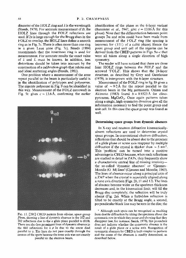
FIG. 11. [201] CBED pattern from olivine, space group Pbnm, showing a line of dynamic absence in the 10E and i02 reflections due to the n glide plane parallel to (010). There are also less prominent lines of dynamic absence in the 0k0 reflections for k r 2n due to the screw diad parallel to y. The lines do not pass exactly through the centres of the spots because the zone axis was not exactly
parallel to the electron beam.
Determining space groups from dynamic absences
In X-ray and neutron diffraction kinematically- absent reflections are used to determine crystal space groups. In conventional electron diffraction, reflections that should be absent due to the presence of a glide plane or screw axis reappear by multiple diffraction if the crystal is thicker than ~ 5 nm 1. This 'problem' can be turned into a positive advantage in C B E D because, when such reflections are studied in detail in ZAPs, they frequently show a characteristic central line of missing intensity-- the so-called 'dynamic absences' or 'Gjonnes- Moodie (G M) lines' (Gjonnes and Moodie, 1965). The lines of absence occur along a principal axis of a ZAP when the crystal is accurately aligned along a zone axis direction (Figs. 2b, 11 and 12). The lines of absence become wider as the specimen thickness decreases and, in the kinematical limit, will fill the Bragg disc completely; the reflection will be truly absent (Fig. 2a). When a forbidden reflection is tilted to be exactly at the Bragg angle, a second, perpendicular black line may be seen in the disc, the
1 Although such spots can be recognised as resulting from double diffraction by tilting the specimen about the systematic row in which they occur and showing that they disappear (see, for instance, Smith, 1978), this procedure does not indicate whether the systematic absence is the result of a glide plane or a screw axis. Recognition of systematic absences by CBED is both simpler to perform and the cause of the absences is readily determined, as described below.

) ) )
)
)
C O N V E R G E N T BEAM E L E C T R O N D I F F R A C T I O N
r t l =
) . . . . . . .
O r
or
r
45
screw diad
glide planes
FIG. 12. Schematic diagram of the appearance of lines of dynamic absence in a CBED pattern. The absence is due either to a screw axis perpendicular to the zone axis or to a glide plane that is either parallel or perpendicular to the zone axis. The glide direction must have a component perpendicular to the zone axis as shown. The cause of the dynamic absence may be determined by examination of the bright-field symmetry. If the mirror line ml is present,
the translational symmetry element is a screw diad, whereas if m z is present the cause is a glide plane.
'black cross', (Steeds, 1981; Steeds and Vincent, 1983) if three dimensional diffraction effects (i.e. HOLZ lines) are relatively weak.
Lines of dynamic absence or black crosses indi- cate either that there is a glide plane with a component of translation perpendicular to the beam or a screw diad axis perpendicular to the beam (Fig. 12). The 41, 43, 61, 63 and 65 screw axes all include the 21 operation. If the sample is thick enough to show H O L Z lines in the BF disc, these two possibilities can be easily distinguished (Steeds and Vincent, 1983). If the mirror line mz is present in the BF disc, the translation symmetry element responsible for the dynamic absence is a screw diad; if the mirror line ml is present, the symmetry responsible is a glide plane.
In Fig. 2b, the dynamic absences in 001 and 003 are the result of both an n-glide parallel to (010) and a screw diad parallel to [001]; the BF disc from a thicker area showed 2mm symmetry. In Fig. 11 the dynamic absence in 102 results from the n-glide parallel to (010); the BF disc showed a mirror line parallel to the line of dynamic absence.
The dynamic absences described above result from dynamic interactions within the zero layer. Double diffraction can also occur in the F O L Z and back again to a kinetically forbidden reflection in the ZOLZ (Gjonnes and Moodie, 1965; Steeds et al., 1978; Steeds and Evans, 1980). In this case
i The 0k0 reflections also show dynamic absences for k ~ 2n due to the screw diad parallel to [010]. Although the b-glide parallel to (100) is also responsible for these forbidden reflections, it does not produce dynamic absences because the glide plane is inclined to the electron beam.
bright H O L Z lines occur on a dark background at the position of the forbidden reflection. Steeds et al., (1978) and Steeds and Evans (1980) observed such 'three dimensional G - M lines' in 200 and 020 reflections in spinel in (001) CBED patterns taken at 100 kV. These reflections are forbidden by the d glide plane in space group Fd3m and cannot reappear by double diffraction within the ZOLZ. Double diffraction between reflections such as 1, 21, 1 and 1, 21, T in the FOLZ, however, does allow reappearance of 200 and 020 (see also Smith, 1978).
It is important to realise that the existence of a line of dynamic absence indicates only that a large proport ion of the intensity in the reflection con- cerned has been derived by multiple scattering. It does not preclude the existence of a small, un- detected, kinematic intensity in the reflection. Steed and Evans (1980) argued that, because the {200}- type reflections in spinel contained three- dimensional G - M lines, the space group was Fd3m and not F743m as had been suggested by Grimes (1972) and Hwang et al. (1973). However, De Cooman and Carter (1985) showed that, although CBED results do not disagree with the assignment of the space group Fd3m to stoichiometric spinel, it is not possible to detect weak, kinematic intensity in the {200}-type reflections due to a small displacement of A1 along (111). Heuer and Mitchell (1975) had estimated the displacement to be 0.002-0.006 A. Such a small displacement would also be insufficient to reduce the whole pattern symmetry of the (100) pattern in fig. 7c from 4ram to 2mm as would be expected for point group F~t3m (see Tables 1-3).

46 P. E. CHAMPNESS
Tanaka et al. (1983) give a table of the lines of dynamic extinction that occur in CBED patterns for all 230 space groups. They conclude that 191 space groups can be identified from the knowledge of the point group, as determined by CBED, the lattice type, as determined kinematically, and the dynamic absences. The remaining 39 space groups are made up of nine pairs of space groups and seven sets of three space groups that cannot be distin- guished from each other by these means. However, they can be distinguished from the intensity change of the forbidden reflections when the crystal orien- tation is varied. An example is the pair 14 and 141 which cannot be distinguished by dynamic absences because the lattice-type absences prohibit double diffraction of the forbidden reflections due to the 41 axis. However, if the intensity of the 200 reflection diminishes appreciably when the orientation is varied, the space group is/41 (Tanaka et al., 1983).
Other information from CBED
Measurement o f foil thickness and extinction distance
If correction is to be made for absorption and fluorescence during the X-ray microanalysis of thin foils, the foil thickness must be known (see Lorimer, this volume). The most accurate method for deter- mining the thickness requires the measurement of the spacing of the diffuse 'Kossel-M611enstedt' fringes that occur in a dark-field disc under two- beam conditions (Kelly et al., 1975). The method is described in detail by Williams (1984). Although accuracies of better than 2% have been claimed, the method is time consuming and it has only been applied so far to simple structures. In the method of Kelly et al., the spacing of the ith minimum is converted to the appropriate deviation parameter Si, which is related to the thickness t, and extinction distance ~g by the equation;
(s , ~ + 1 / ~ ) t : = n~ where n i is an integer and ni+a = n~+ 1.
If ~, is known, graphs of (Si/ni) 2 versus 1/n~ can be plotted for various possible values of nl. The straight line which shows a slope of 1/~g 2 is the correct one and the thickness is obtained from the intercept, 1/t z, on the 1/n 2 axis.
Unfortunately there are a number of problems associated with this method, particularly where minerals are concerned. Generally, extinction distances are not known for mineral structures. Thus knowledge of the extinction distance cannot be used to determine which line is the correct one. In addition, it is difficult to avoid multiple-beam interactions in minerals because of small reciprocal
lattice spacings. Such effects will introduce a systematic error (Allen, 1981). Assessment of the effect of anomalous absorption and inelastic scattering should also be made (Allen and Hall, 1982; Castro-Fernandez et al., 1985). Two-beam dynamical calculations that take into account absorption have been made by Castro-Fernandez et al. (1985) for copper samples. Curves for various values of t/~g, nl and ~g/~'g (the absorption coeffi- cient) were computed and compared with experi- mental curves obtained with a densitometer from the diffraction patterns. The best fit allowed assignment of nl and hence determination of t and cg to an accuracy of _+ 5% or better.
Clearly calculations taking into account multiple- beam interactions and anomalous absorption need to be carried out in order to assess the applicability of the method to minerals. Even then it must be borne in mind that the total specimen thickness would be underestimated because the amorphous layer that is produced on both sides of the specimen by ion-beam thinning would not be 'seen' by the electrons. A further limitation on the applicability of the technique to minerals arises from the fact that at least three dark fringes must be visible in the Kossel-M611enstedt pattern. Many low-index re- flections from minerals may have too small a g value for them to show three fringes in non- overlapping discs.
Determination o f cell parameters One of the limitations of selected-area electron
diffraction is that, unless an internal standard is used, accurate lattice parameters cannot be ob- tained. However, small changes in lattice para- meters of the specimen produce relatively large shifts in the HOLZ lines in CBED patterns.
If the positions of the HOLZ lines in the BF disc of a cubic material are compared with the equiva- lent pattern taken at exactly the same voltage from a standard material with the same crystal structure, the lattice parameter can be determined (Steeds, 1979). Alternatively, the HOLZ patterns can be simulated by computer for different values of a once the HOLZ lines have been indexed (Ecob et al., 1981). The best fit will indicate the actual cell parameter (Shaw et al., 1981). Lattice parameters that vary by _+ 0'005 ~, can easily be distinguished by this means. However, any slight variation in the accelerating voltage from that assumed in the calculations will affect the accuracy.
Vincent and Pretty (1986) recently extended the method to the determination of the cell parameters of an orthorhombic phase. NiP1.8Geo. 2 was found by convergent-beam methods to have the space group Pnnm and measurement of the unit cell parameters suggested that the phase has the

C O N V E R G E N T BEAM E L E C T R O N D I F F R A C T I O N 47
structure of marcasite, FeS2. [111] C B E D patterns were taken for NiPl.sGeo. 2 and for marcasite. Deficiency H O L Z lines within the BF disc were indexed and a set was chosen that were both sen- sitive to changes in all three cell parameters and showed no visible dynamic coupling at intersections. Published values for the cell parameters of marcasite were used in a computer simulation of the H O L Z lines at different excitation voltages. The exact voltage having been determined, the cell parameters were systematically varied, until a match was found with the experimental pattern for NiP1.8GeOo. 2. The estimated accuracy of the lattice parameters determined by the method approached one part in 1000.
Conclusion
The recent exploitation of convergent beam electron diffraction has transformed electron dif- fraction from being considered the 'poor relation' of X-ray and neutron diffraction for crystallographic studies to being, in many ways, superior to these techniques. The breakdown of Friedel's law in electron diffraction allows the point group of a crystalline material to be determined when a con- vergent beam is used. Often the information can be obtained from a set of patterns from a single zone axis. Even the so-called 'problem' of double diffrac- tion can be turned to advantage in identifying translational symmetry elements and hence in determining the space group. All this information can, in principle, be obtained from crystals as small as 50 nm.
CBED can be used, in principle, to determine the thickness of the specimen and the extinction distance, although the necessary calculations have not been carried out for minerals. Accurate cell parameters can also be obtained for cubic minerals or in cases where a suitable standard is available.
Acknowledgements
I would like to thank M. G. Bown, C. Hammond, P. B. Kenway and R. Vincent for valuable com- ments on this paper. The Philips EM 400T electron microscope used in this work was partially funded by grant GR3/3580 from the Natural Environment Research Council. The work on Mg germanates is partially funded by N E R C grant GR3/5660. I am grateful to I. Bough, S. Caldwell, G. Cliff and P. B. Kenway for technical assistance.
References
Akizuki, M., Hampar, M. S. and Zussman, J. (1979) Mineral. Mag. 43, 237.
Allen, F. M., Buseck, P. R. and Rossman, G. R. (1986) Geol. Soc. Am. Abst. with Program 18, 525.
Allen, S. M. (1981) Phil. Mag. A43, 325. - - a n d Hall, E. L. (1982) Ibid. 46, 243. Bannister, F. A., Hey, M. A. and Stadler, H. P. (1947)
Mineral Mag. 28, 129. Buxton, B. F., Eades, J. A., Steeds, J. W. and Rackham,
G. M. (1976) Phil. Trans. Roy. Soc. 281A, 171. Castro-Fernandes, F. R., Sellars, C. M. and Whiteman,
J. A. (1985) Phil. Mag. A52, 289. Cliff, G. and Kenway, P. B. (1982) Proc. Microbeam Anal.
Soc. 107. De Cooman, B. C. and Carter, C. B. (1985) Phil. Ma9.
A51, 175. Eades, J. A., Shannon, M. D. and Buxton, B. F. (1983)
Scanning Electron Microscopy 1983 31. (O. Johari, ed.). SEM Inc. AMF O'Hare, Illinois, 1051.
Ecob, R. C., Shaw, M. P., Porter, A. J. and Ralph, B. (1981) Phil. Mag. A44, 1117.
Gjonnes, J. and Moodie, A. F. (1965) Acta Crystallogr. 19, 65.
Goodman, P. (1975) Ibid. A3t, 804. and Johnson, A. W. S. (1977) Ibid. A33. 997.
Grey, I. E. and Gatehouse, B. M. (1979) Am. Mineral. 64, 1255.
Grimes, N. W. (1972) Phil. Mag. 26, 1217. Heuer, A. H. and Mitchell, T. E. (1975) J. Phys. Chem. 8,
L541. Hwang, L., Heuer, A. H. and Mitchell, T. E. (1973) Phil.
Mag. 28, 241. Kelly, P. M., Jostens, A., Blake, R. G. and Napier, J. G.
(1975) Phys. Star. Sol. A31, 771. Kossel, W. and M611enstedt, G. (1939) Ann. Phys. 36,
113. Loretto, M. H. (1984) Electron Beam Analysis of
Materials. Chapman and Hall, London. Neder, R. B. W. (1985) M.S. Thesis, Arizona State
University. Ozima, M. and Akimoto, S.-I. (1983) Am. Mineral. 68,
1199. Porter, A. J., Shaw, M. P., Ecob, R. C. and Ralph, B. (1981)
Phil. Mag. A44, 1135. Shaw, M. P., Ecob, R. C., Porter, A. J. and Ralph, B.
(1981) In Quantitative Microanalysis with High Spatial Resolution, The Metals Society, London, 229.
Smith, P. P. K. (1978) Phil. Mag. B38, 99. - - ( 1 9 8 0 ) Geol. Ma 9. 117, 385. Steeds, J. W. (1979) In Introduction to Analytical Electron
Microscopy (J. J. Hren, J. I. Goldstein and D. C. Joy, eds.) Plenum Press, New York, 387.
- - ( 1 9 8 1 ) In Quantitative Microanalysis with High Spatial Resolution, The Metals Society, London, 210.
- - ( 1 9 8 4 ) In Quantitative Electron Microscopy (J. N. Chapman and A. J. Craven, eds.) Scottish Univ. Summer School in Physics.
- - a n d Evans, N. S. (1980) Proc. Electron Microscopy Society of America. 38th Ann. Meeting. Claitor's Pub- lishing, 188.
- - a n d Vincent, R. (1983) J. Appl. Crystalloor. 16, 317. - - R a c k h a m , G. M. and Shannon, M. D. (1978) Inst.
Phys. Conf. Ser. 41, 135. - - a n d the Bristol Group (1984) Convergent Beam

48 P. E. C H A M P N E S S
Electron Diffraction of Alloy Phases (J. Mansfield, ed.). Hilger, Bristol.
Tanaka, M., Seikii, H, and Nagasawa, J. (1983) Acta Crystallogr. A39, 825.
Vincent, R. and Pretty, S. F. (1986) Phil. Mag. A53, 843.
Williams, D. B. (1984) Practical Analytical Electron Microscopy in Materials Science. Philips Electronic Instruments. Inc., New Jersey, 153 pp.
[Revised manuscript received 1 September 1986]