Embed Size (px)
Citation preview

Marquette Universitye-Publications@Marquette
Physics Faculty Research and Publications Physics, Department of
9-1-2010
Controlling Individual Domain Walls inFerromagnetic Nanowires for Memory and SensorApplicationsAndrew KunzMarquette University, [email protected]
Sarah C. Reiff
Jonathan D. Priem
Eric W. Rentsch
Accepted version. Published as a part of the conference 2010 ICEAA Offshore/IEEE Xplore, 2010:248-251. DOI.© 2010 IEEE. Reprinted, with permission, from Andrew Kunz, Sarah C. Reiff, Jonathan d. Priem,Eric W. Rentschle, Controlling individual domain walls in ferromagnetic nanowires for memory andsensor applications, Proceedings of 2010 ICEAA Offshore/IEEE Xplore, September 2010.This material is posted here with permission of the IEEE. Such permission of the IEEE does not inany way imply IEEE endorsement of any of Marquette University’s products or services. Internal orpersonal use of this material is permitted.However, permission to reprint/republish this material for advertising or promotional purposes orfor creating new collective works for resale or redistribution must be obtained from the IEEE bywriting to [email protected]. By choosing to view this document, you agree to allprovisions of the copyright laws protecting it.
NOT THE PUBLISHED VERSION; this is the author’s final, peer-reviewed manuscript. The published version may be accessed by following the link in the citation at the bottom of the page.
Proceedings of 2010 ICEAA Offshore/IEEE Xplore, (September 2010): pg. 248-251. DOI. This article is © Institute of Electrical and Electronics Engineers (IEEE) and permission has been granted for this version to appear in e-Publications@Marquette. Institute of Electrical and Electronics Engineers (IEEE) does not grant permission for this article to be further copied/distributed or hosted elsewhere without the express permission from Institute of Electrical and Electronics Engineers (IEEE).
1
Controlling Individual Domain Walls
in Ferromagnetic Nanowires for
Memory and Sensor Applications
Andrew Kunz Physics Department, Marquette University,
Milwaukee, WI
Sarah C. Reiff Physics Department, Marquette University,
Milwaukee, WI
Jonathan D. Priem Physics Department, Marquette University,
Milwaukee, WI
Eric W. Rentsch Physics Department, Marquette University,
Milwaukee, WI
Controlled motion of 180° and 360° domain walls along planar
nanowires is presented. Standard Landau — Lifshitz micromagnetic modeling
has been used to simulate the response of the domain walls to the application
of an external magnetic field. A 180° wall is quickly and easily moved with the
application of an applied. field along the axis of the wire but a 360°domain
wall is stationary in the same case. An oscillatory applied field can be used to
continually move the wall along the wires axis. The speed at which the 360°
domain wall is found to be several times slower than a similar 180° domain
NOT THE PUBLISHED VERSION; this is the author’s final, peer-reviewed manuscript. The published version may be accessed by following the link in the citation at the bottom of the page.
Proceedings of 2010 ICEAA Offshore/IEEE Xplore, (September 2010): pg. 248-251. DOI. This article is © Institute of Electrical and Electronics Engineers (IEEE) and permission has been granted for this version to appear in e-Publications@Marquette. Institute of Electrical and Electronics Engineers (IEEE) does not grant permission for this article to be further copied/distributed or hosted elsewhere without the express permission from Institute of Electrical and Electronics Engineers (IEEE).
2
wall and is limited by interaction between the magnetization of the domain
wall and the external field.
Section 1: Introduction
A magnetic domain wall is the transition region between
oppositely magnetized domains. This transition region can be put into
motion with the application of an external magnetic field or with a
spin-polarized current via a spin-torque effect1,2. Each driving
mechanism has its advantages over the other but in principle the
dynamics of the moving wall are the same and ultimately a
combination of the two effects is likely to be necessary. Several
spintronic devices in logic, recording, and sensing have been proposed
which utilize the motion of a domain wall along the axis of a thin,
narrow nanowire to transmit or store information3,4. The realization of
these devices depends in part on the ability to control the location of
the domain wall in the wire.
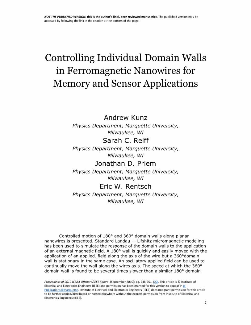
In a thin enough nanowire there is essentially one type of
domain wall, a transverse or 180° domain wall where the
magnetization rotates in the plane of the wire as it transitions from
one direction to the other as shown at the top of Figure 1 [5]. The
bottom image shows two transverse walls which have been pushed
together to create a full rotation of the magnetization. This extremely
stable structure is called a 360° domain wall and it considered a
transition between two aligned domains. Arrows representing the
direction of the magnetic moments are included in Figure 1 to show
how the transition occurs. The red and blue shading correspond to the
direction of the long axis magnetization and the scheme remains the
same throughout this manuscript.
Controlling a domain wall requires involves both moving the wall
and stopping it. For device operation it is preferential to move the wall
quickly. The 180° domain wall is easily, and quickly, moved with the
application of an external magnetic field oriented along the long axis of
the wire. The wall moves as the domain in the direction of the applied
field grows at the expense of the oppositely magnetized domain, which
leads to an overall reduction in Zeeman energy. A 360° domain wall is
not easily moved however. When a field is applied along the main
magnetization direction, to the right in Figure 1, the left and right
NOT THE PUBLISHED VERSION; this is the author’s final, peer-reviewed manuscript. The published version may be accessed by following the link in the citation at the bottom of the page.
Proceedings of 2010 ICEAA Offshore/IEEE Xplore, (September 2010): pg. 248-251. DOI. This article is © Institute of Electrical and Electronics Engineers (IEEE) and permission has been granted for this version to appear in e-Publications@Marquette. Institute of Electrical and Electronics Engineers (IEEE) does not grant permission for this article to be further copied/distributed or hosted elsewhere without the express permission from Institute of Electrical and Electronics Engineers (IEEE).
3
walls remain stationary, essentially pushing up against each other. The
robustness of the 360° wall to applied fields is a desired feature for
recording information therefore moving the wall to a desired location is
critical. If the field is applied in the reverse direction, to the left, the
walls separate but they move with the same speed so the “center” of
the overall transition region remains stationary. A current might be
useful in this case as it has been shown that currents move domain
walls in the same direction, although typically an order of magnitude
slower than a field moves the wall. Here we present a technique for
moving the 360° domain wall with applied fields with minimum speeds
equivalent to that found in fast current driven cases1.
Figure 1: Representations for the magnetic moments of a 180° and 360°
domain wall in a 100 nm wide wire
Once a simple transverse wall is in motion there are several
techniques available for stopping it. Most techniques rely on a change
to the physical shape or magnetic structure of the wire, often a notch
or protrusion in the wire itself8,9. Because these artificial defects must
be added ahead of time, during the manufacturing of the wire,
precision control of the domain walls can be obtained but there is no
possibility of changing the trapping locations. Additionally, a trapped
domain wall is often difficult to release, requiring large fields or
currents to put the wall into motion again10. Additional control of
domain wall pinning locations could be realized if the pinning sites
could be moved as opposed to set when built. Recently it was
proposed that domain walls could be used as traps for other domain
walls in neighboring wires11,12. The domain walls would couple together
across the wires and could allow for an additional degree of control if
the 360° walls could be reliably moved. In this work we present our
NOT THE PUBLISHED VERSION; this is the author’s final, peer-reviewed manuscript. The published version may be accessed by following the link in the citation at the bottom of the page.
Proceedings of 2010 ICEAA Offshore/IEEE Xplore, (September 2010): pg. 248-251. DOI. This article is © Institute of Electrical and Electronics Engineers (IEEE) and permission has been granted for this version to appear in e-Publications@Marquette. Institute of Electrical and Electronics Engineers (IEEE) does not grant permission for this article to be further copied/distributed or hosted elsewhere without the express permission from Institute of Electrical and Electronics Engineers (IEEE).
4
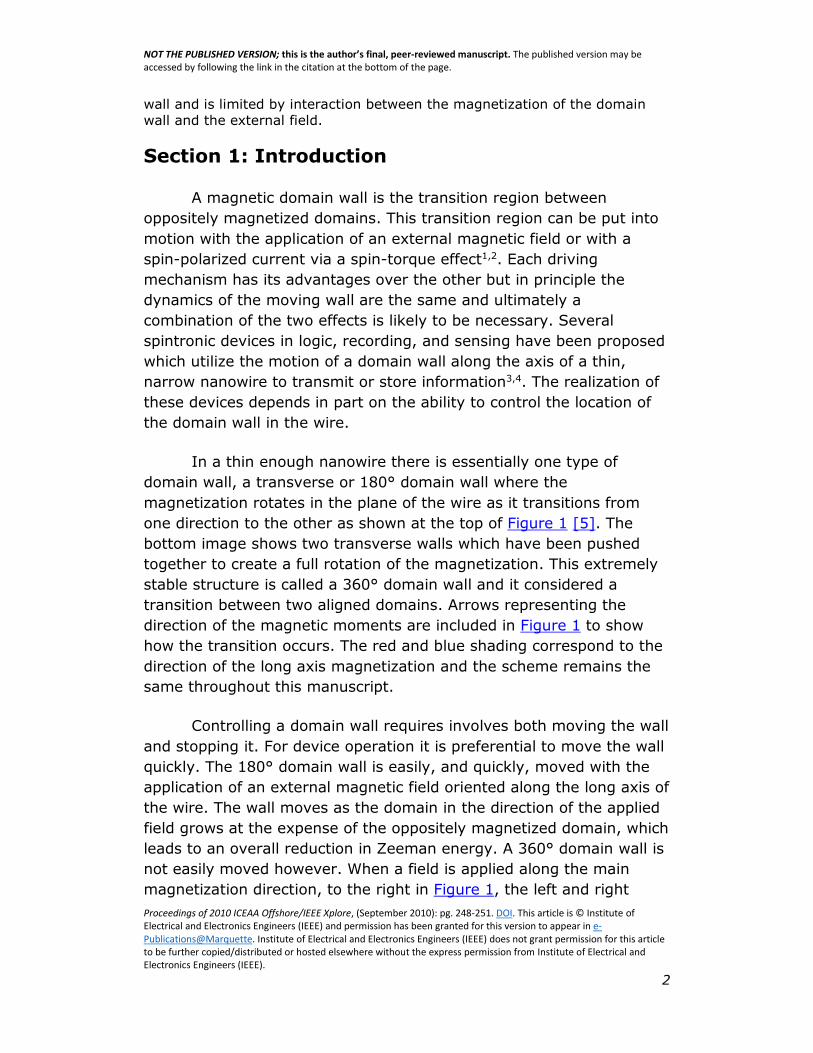
technique for controlling the location of a 360° domain wall. Our
technique controls the location of the wall by systematically controlling
the external field pulse durations and directions used to move the wall.
Figure 2: Time lapse sequence of domain walls being injected and trapped in
a wire with magnetic fields.
Section 2: Simulation Details
We simulate the motion of a domain wall with standard three-
dimensional micromagnetic simulation. The simulations follow the
standard Landau-Lifshitz equation of motion for the magnetic moments
m in the wire
𝜕�⃗⃗�
𝑑𝑡 = −𝛾�⃗� × 𝐻 −
𝛼𝛾
𝑀𝑠�⃗⃗� × (�⃗⃗� × �⃗⃗� )
where γ is the gyromagnetic ratio, Ms is the saturation magnetization
and H is the total magnetic field acting on a magnetic moment13. The
materials parameters are for permalloy. The simulated wires have a
length of 10 microns and a 100 × 5 nm2 rectangular cross-section. The
wire is discretized into identical cubes, no larger than 5nm on edge
and integrated with a 4th order predictor corrector technique with a
NOT THE PUBLISHED VERSION; this is the author’s final, peer-reviewed manuscript. The published version may be accessed by following the link in the citation at the bottom of the page.
Proceedings of 2010 ICEAA Offshore/IEEE Xplore, (September 2010): pg. 248-251. DOI. This article is © Institute of Electrical and Electronics Engineers (IEEE) and permission has been granted for this version to appear in e-Publications@Marquette. Institute of Electrical and Electronics Engineers (IEEE) does not grant permission for this article to be further copied/distributed or hosted elsewhere without the express permission from Institute of Electrical and Electronics Engineers (IEEE).
5
simulated integration time step of less than a picoseconds. The
magnetic damping parameter is α=0.008.
To put the walls in motion magnetic fields are applied along the
long axis of the wire. We keep the moving wall field strength below the
so-called Walker breakdown field to maintain the domain walls of a
known shape and because this is the field range for which the walls
move the quickest.
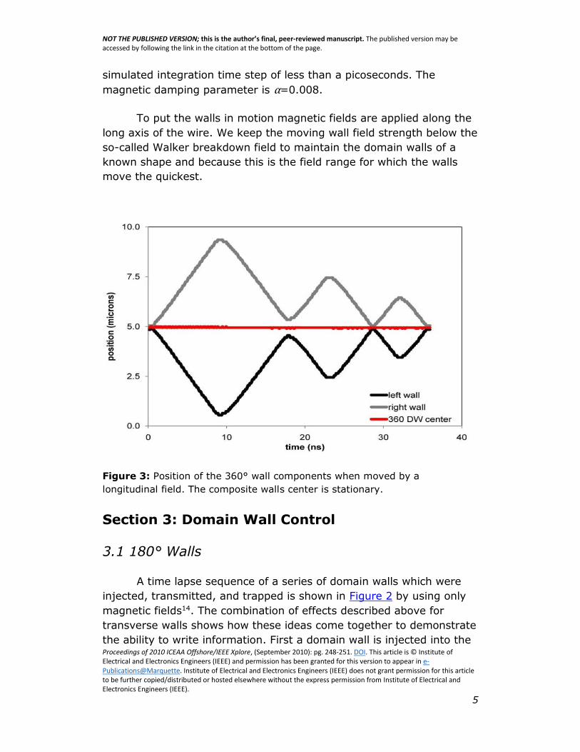
Figure 3: Position of the 360° wall components when moved by a
longitudinal field. The composite walls center is stationary.
Section 3: Domain Wall Control
3.1 180° Walls
A time lapse sequence of a series of domain walls which were
injected, transmitted, and trapped is shown in Figure 2 by using only
magnetic fields14. The combination of effects described above for
transverse walls shows how these ideas come together to demonstrate
the ability to write information. First a domain wall is injected into the

NOT THE PUBLISHED VERSION; this is the author’s final, peer-reviewed manuscript. The published version may be accessed by following the link in the citation at the bottom of the page.
Proceedings of 2010 ICEAA Offshore/IEEE Xplore, (September 2010): pg. 248-251. DOI. This article is © Institute of Electrical and Electronics Engineers (IEEE) and permission has been granted for this version to appear in e-Publications@Marquette. Institute of Electrical and Electronics Engineers (IEEE) does not grant permission for this article to be further copied/distributed or hosted elsewhere without the express permission from Institute of Electrical and Electronics Engineers (IEEE).
6
wire from the pad on the left. The wall is then quickly driven along the
length of the wire until it is trapped at a notch. The elapsed time
between “0 0 0” and “0 0 1” was under 2 ns. The now trapped wall is
stationary as the subsequent domain walls are injected and moved in
to location. A three bit sequence, in Figure 2 a “1” or a “0” depends on
the presence of a domain wall at a trapping point, has 8 possible
states so this structure represents the minimum necessary for writing
information quickly and reliably. Four of the eight representations are
shown. The final “1 1 1” sequence was written in under 6 ns.
3.2 360° Walls
Stopping a 360° domain wall is as easy as letting the two
transverse walls collide under a compressive field (field that moves the
walls toward each other). The two colliding transverse walls couple
together to create a robust 360° domain wall. Figure 3 shows the
difficulty in moving a 360° domain wall. The plot shows the position of
the left and right walls as a function of time as a magnetic field is
applied along the long axis of the wire. Initially the field drives the
walls quickly apart. When the field is later reversed, the domain walls
turn around and move together.
NOT THE PUBLISHED VERSION; this is the author’s final, peer-reviewed manuscript. The published version may be accessed by following the link in the citation at the bottom of the page.
Proceedings of 2010 ICEAA Offshore/IEEE Xplore, (September 2010): pg. 248-251. DOI. This article is © Institute of Electrical and Electronics Engineers (IEEE) and permission has been granted for this version to appear in e-Publications@Marquette. Institute of Electrical and Electronics Engineers (IEEE) does not grant permission for this article to be further copied/distributed or hosted elsewhere without the express permission from Institute of Electrical and Electronics Engineers (IEEE).
7
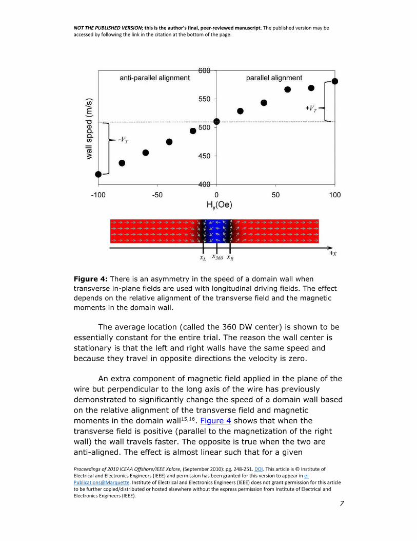
Figure 4: There is an asymmetry in the speed of a domain wall when
transverse in-plane fields are used with longitudinal driving fields. The effect
depends on the relative alignment of the transverse field and the magnetic
moments in the domain wall.
The average location (called the 360 DW center) is shown to be
essentially constant for the entire trial. The reason the wall center is
stationary is that the left and right walls have the same speed and
because they travel in opposite directions the velocity is zero.
An extra component of magnetic field applied in the plane of the
wire but perpendicular to the long axis of the wire has previously
demonstrated to significantly change the speed of a domain wall based
on the relative alignment of the transverse field and magnetic
moments in the domain wall15,16. Figure 4 shows that when the
transverse field is positive (parallel to the magnetization of the right
wall) the wall travels faster. The opposite is true when the two are
anti-aligned. The effect is almost linear such that for a given

NOT THE PUBLISHED VERSION; this is the author’s final, peer-reviewed manuscript. The published version may be accessed by following the link in the citation at the bottom of the page.
Proceedings of 2010 ICEAA Offshore/IEEE Xplore, (September 2010): pg. 248-251. DOI. This article is © Institute of Electrical and Electronics Engineers (IEEE) and permission has been granted for this version to appear in e-Publications@Marquette. Institute of Electrical and Electronics Engineers (IEEE) does not grant permission for this article to be further copied/distributed or hosted elsewhere without the express permission from Institute of Electrical and Electronics Engineers (IEEE).
8
transverse field strength that each walls speed changes by the same
magnitude VT. This allows for the systematic control of a 360° domain
wall as shown in Figure 5. Initially, along path A, a magnetic field is
applied along the long axis of the wire to separate the two walls and a
transverse field is used to move the right wall more quickly than the
left wall. The fields are reversed causing the walls to move back
toward each other. This time the reversal of the transverse field, along
path B, moves the left wall quicker than the right so that when the two
walls approach each other at C. This process is repeated until the wall
has been moved a 2.5 microns. The average speed of the domain wall
center is roughly 85 m/s. This is about an order of magnitude less than
the 500 m/s a single transverse wall moves but it is consistent to the
maximum speed observed for a single wall driven by an electric
current and the first report of moving a 360° domain wall with applied
fields.
Figure 5: Transverse fields are used to move 3600 domain walls significant
distances by oscillating the field components. The wall averages 85 m/s.

NOT THE PUBLISHED VERSION; this is the author’s final, peer-reviewed manuscript. The published version may be accessed by following the link in the citation at the bottom of the page.
Proceedings of 2010 ICEAA Offshore/IEEE Xplore, (September 2010): pg. 248-251. DOI. This article is © Institute of Electrical and Electronics Engineers (IEEE) and permission has been granted for this version to appear in e-Publications@Marquette. Institute of Electrical and Electronics Engineers (IEEE) does not grant permission for this article to be further copied/distributed or hosted elsewhere without the express permission from Institute of Electrical and Electronics Engineers (IEEE).
9
Section 4: Discussion
The maximum speed of a 360° domain wall is a function of the
transverse field. Larger transverse fields should lead to faster overall
speeds. As shown in Figure 4 we define the center of the domain wall,
x360, to be the average position of the left, xL, and right, xR. walls
𝑥360 =𝑥𝐿 + 𝑥𝑅
2.
The position of each wall as a function of time is x(t)R,L=νR,Lt where the subscripts correspond to the left and right walls individually.
When a transverse field is applied parallel to the moments in the right
wall (anti-parallel to the left) the velocity of each wall changes in
proportion by
νR=ν0+VT
νL=−(ν0−VT)=−ν0+VT.
Where ν0 is the speed with no transverse field and VT is the speed
change due to the transverse field. This means that the domain wall
center is located at
𝑥360 =(−𝜈0 + 𝑉𝑇)𝑡 + (𝜈0 + 𝑉𝑇)𝑡
2= 𝑉𝑇𝑡.
When the field are reversed the velocities of the walls change in
magnitude and direction such that
νR=−(ν0−VT)=−ν0+VT
νL=ν0+VT
the center of the domain wall continues to move forward with the
speed gained by the application of the transverse field
𝑥360 = (𝜈0 + 𝑉𝑇)𝑡 + (−𝜈0 + 𝑉𝑇)𝑡
2= 𝑉𝑇𝑡.

NOT THE PUBLISHED VERSION; this is the author’s final, peer-reviewed manuscript. The published version may be accessed by following the link in the citation at the bottom of the page.
Proceedings of 2010 ICEAA Offshore/IEEE Xplore, (September 2010): pg. 248-251. DOI. This article is © Institute of Electrical and Electronics Engineers (IEEE) and permission has been granted for this version to appear in e-Publications@Marquette. Institute of Electrical and Electronics Engineers (IEEE) does not grant permission for this article to be further copied/distributed or hosted elsewhere without the express permission from Institute of Electrical and Electronics Engineers (IEEE).
10
This simple calculation shows that the 360° wall cannot move
without the transverse fied. Additionally it is instructive to compare the
results of the simulation with this simple calculation. We measure
VT=110m/s in this trial, whereas we measure a speed for the domain
wall of 85 m/s which is in good agreement. The bulk of the difference
comes from the reversal of the domain walls as noticed in Figure 5.
When the fields are reversed the walls stop and turn around slowing
the overall progress. The simple calculation above represents the
maximum speed a 360° domain wall could move which will be slowed
by the necessary field reversals. In a long wire the reversals could be
minimized because there would be more room for the walls to move,
whereas in our 10 micron simulation we had to reverse the fields to
keep the walls from leaving the ends of the wire.
Section 5: Conclusion
Magnetic fields are used to quickly move and control the
location of 360° domain walls in thin, narrow nanowires. A 360°
domain wall moves with a maximum speed determined by the strength
of a transverse field which is necessary to propagate the wall. This
speed is slower than typically found for a 180° domain wall but still
fast when compared to similar efforts using electric currents as the
driving mechanism. The precise location of the 360° domain wall can
be controlled without making physical changes to the wire. Instead
controlling the length of the field pulse determines how far the wall will
move which gives an extra degree of control for tuning the wall
location.
Acknowledgments
This work was supported by the National Science Foundation under
Grant DMR-0706194.
References
1. Yamaguchi, A., "Real-space observation of current-driven domain wall
motion in submicron magnetic wires", Phys. Rev. Lett., vol. 92, no.7,
pp.077205, 2004
2. Schryer, N. L., Walker, L. R., "The motion of 180 degree domain walls in
uniform dc magnetic fields", J. Appl. Phys., vol. 45, no.12, pp.5406-21, 1974
NOT THE PUBLISHED VERSION; this is the author’s final, peer-reviewed manuscript. The published version may be accessed by following the link in the citation at the bottom of the page.
Proceedings of 2010 ICEAA Offshore/IEEE Xplore, (September 2010): pg. 248-251. DOI. This article is © Institute of Electrical and Electronics Engineers (IEEE) and permission has been granted for this version to appear in e-Publications@Marquette. Institute of Electrical and Electronics Engineers (IEEE) does not grant permission for this article to be further copied/distributed or hosted elsewhere without the express permission from Institute of Electrical and Electronics Engineers (IEEE).
11
3. Allwood, D. A., "Magnetic domain-wall logic", Science, vol. 309, pp.1688-
92, 2005
4. Parkin, S. S.P., Hayashi, M, Thomas, L., "Magnetic Domain wall racetrack
memory", Science, vol. 320, pp.190-194, 2008
5. McMichael, R.D., Donahue, M.J., "Head to head domain wall structures in
thin magnetic strips", IEEE Trans. Magn., vol. 33, no.5, pp.4167-9, 1997
6. Castano, F.J., "Metastable staes in magnetic nanorings", Phys. Rev. B, vol.
67, no.18, pp.184425, 2003
7. Chaves-O'Flynn, G.D., "Stability of 21π Domain Walls in Ferromagnetic
Nanorings", IEEE Trans. Magn., vol. 46, no.6, pp.2272, 2010
8. Petit, D., Jausovec, A.-V, Read, D., Cowburn, R. P., "Domain wall pinning
and potential landscapes created by constrictions and protrusions in
ferromagnetic nanowires", J. Appl. Phys., vol. 103, no.11437, 2008
9. Vogel, A., "Domain-Wall Pinning and Depinning at Soft Spots in Magnetic
Nanowires", IEEE Trans. Magn., vol. 46, no.6, pp.1708, 2010
10. A. Kunz, J. Priem, "Static and Dynamic Pinning Fields for Domain Walls in
Ferromagnetic Nanowires", IEEE Trans. Magn., vol. 46, no.6, pp.1559, 2010
11. O'Brien, L., "Near-field interaction between domain walls in adjacent
permalloy nanowires", Phys. Rev. Lett., vol. 103, pp.077206, 2009
12. Hayward, T. J., "Direct imaging of domain-wall interactions in Ni80Fe20
planar nanowires", Phys. Rev. B, vol. 81, pp.020410, 2010
13. Mircomagnetic Simulator, http://llgmicro.home.mindspring.comv.2.61
14. A. Kunz, S.C. Reiff, "Dependence of domain wall structure for low field
injection into magnetic nanowires", Aplp. Phys. Lett., vol. 94, no.192504,
2009
15. A. Kunz, S. C. Reiff, "Enhancing domain wall speed in nanowires with
transverse magnetic fields", J. Appl. Phys., vol. 103, no.07D903, 2008
16. Richter, K., Varga, R., Badini-Confalonieri, Vazquez, M., "The effect of
transverse field on fast domain wall dynamics in magnetic nanowires", Appl.
Phys. Lett., vol. 96, pp.182507, 2010