Embed Size (px)
Citation preview
CONTROLLING DEVICE VIA THE INTERNET
MAIIATILIR BIN BADRIJL ZAMAN
A thesis submitted in fulfillment of the
requirements for the award of the degree
Bachelor of Computer Science (Computer Systems & Network)
Faculty of System Computer & Software Engineering
University College of Engineering and Technology Malaysia
November 2005

ABSTRACT
Internet had been used as a line of communication and wireless
technology had enabled the drastic increase in internet usage. With better
communication technology trend, the opportunity of creating various application
systems using internet will be greatly demanded. Currently, the lab administrator
at Faculty of Computer System& Software Engineering FSKKP) had to manage
the lab facilities manually. This has leads to slowness in managing the lab that
distract their main task which is to attend to the lab directly. The main purpose of
this system is to control the lab facilities through internet. A prototype of the
system is developed to assist the lab administrator to control the lab facilities
through internet. This would certainly improve the productivity. Other than that it
also will make harmful to user if there are in rush. By implement this project it
can help to control the devices whenever and wherever user wants only by using
fingertip.
lv

ABSTRAK
Internet merupakan satu rangkaian komurnkasi yang sangat penting
sehingga penggunaanya sangat diperlukan masa kini. Dengan perhubungan
komunikasi yang lebih baik maka kelebihan membina sesuatu aplikasi
menggunakan perantaraan internet sangat dikehendaki. Buat masa sekarang juru
makmal di Fakulti Sistem Komputer dan Kejuruteraan Perisian (FSKKP) terpaksa
mengawal sernua pekakasan secara manual. mi menyebabkan kebanyakan
tugasan lambat disiapkan termasuk pengawasan makmal sehingga menyebabkan
tugasan mereka dalam mengendalikan makmal terganggu. Tujuan utama projek
mi adalah untuk mengawal pekakasan di makmal menggunakan rangkaian
internet. Satu model sistem mi telah di bina untuk membantujuru makmal dalam
mengawal pekakasan menerusi internet. mi sekaligus dapat meningkatkan
produktiviti kerja . Dengan menggunakan projek mi juga diharapkan ia dapat
membantu dalam mengawal pekakasan dimana sahaja.
V
TABLE OF CONTENTS
CHAPTER TITLE PAGE
TITLE PAGE i
DECLARATION
ACKNOWLEDGEMENT
ABSTRACT
ABSTRAK v
TABLE OF CONTENT vi
LIST OF TABLE x
LIST OF FIGURES xi
LIST OF ABBREVIATION xii
LIST OF SYMBOLS xiv
LIST OF APPENDICES xv
1. INTRODUCTION
1.1 Overview I
1.2 Problem Statements 3
1.3 Objective 3
1.4 Scopes 3
1.5 Project Contribution 3
vi

2. LITERATURE REVIEW
2.1 Introduction 5
2.2 PC Board layout 7
2.3 Circuit 8
2.3.1 Design schematic circuit 9
2.3.2 Design PCB 9
2.3.3 Exposing 9
2.3.4 Developing 9
2.3.5 Etching 9
2.3.6 Drilling 10
2.3.7 Remove stain 10
2.3.8 Tin plating 11
2.3.9 Drying 11
2.3.10 Soldering 11
2.3.11 Complete circuit 12
2.4 Inpout32.dll 14
2.4.1 How Inpout32.dll Works 14
2.4.2 The DLL Inpout32 15
2.5 Introduction to Parallel Port 16
2.6 Hardware Properties 19
2.7 communicating Through Parallel Port 21
2.7.1 Using the Parallel Port to Input 8 Bits 23
2.8 Introduction to Visual Programming 24
2.8.1 Visual Basic Ins and Outs 25
2.8.2 Good graphic 25
2.8.3 Light Work 26
2.9 Introduction to ASP Programming 27
2.9.1 ASP Compatibility 27
vii

viii
2.9.2 How Does ASP Differ from HTML 27
2.9.3 How Does ASP Works 28
2.10 Literature of Integrated Circuit (IC) 29
3 METIJADOLOGY
3.1 Introduction 30
3.2 Project Identification Phase 31
3.3 Project Planning Phase 32
3.4 Analysis Phase 32
3.5 Project Design Phase 32
35.1 Design for Output Circuit 33
3.5.2 Design for System 35
3.5.2 Project Flow 36
3.6 Implementation and Testing Phase 38
3.6.1 Coding Testing 38
3.6.2 Hardware for Testing Sample Program 39
3.6.3 Circuit Testing 39
3.6.4 Installation Testing 45
3.6.5 System Requirement 46
4 RESULT AND DISCUSSION
4.1 Introduction 47
4.2 Result 47
4.3 Relay Control through Button Click 51
4.4 Programming for Devices 52
4.5 Flow Chart of Login Process 54
4.6 Discussion
4.7 Assumption and Constraints 56

Ix
4.8 Further Research
57
CONCLUSION
5.1 Summary 58
REFERENCE
60
APPENDICES A
APPENDICES B
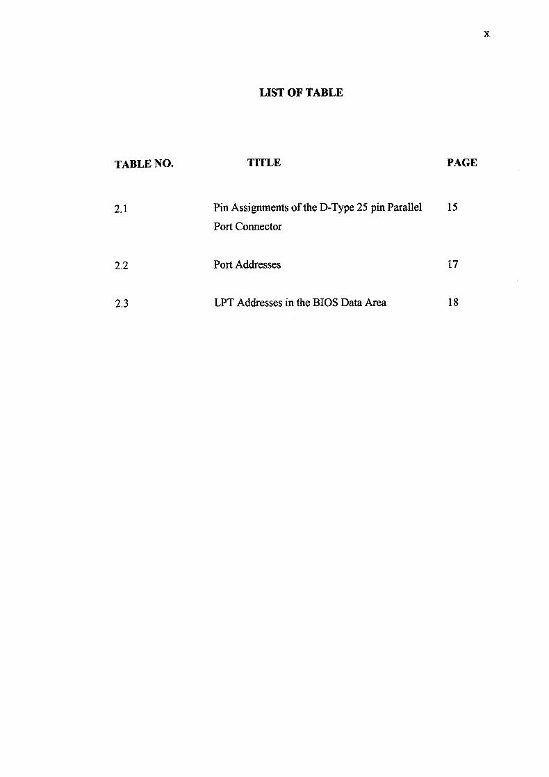
LIST OF TABLE
TABLE NO. TITLE
PAGE
2.1 Pin Assignments of the D-Type 25 pin Parallel 15
Port Connector
2.2 Port Addresses
17
2.3 LPT Addresses in the BIOS Data Area 18
x

LIST OF FIGURES
FIGURE NO TITLE IPAGE
1.1 Overview diagram of controlling device via
Internet 2
2.1 Block Diagram of controlling device via Internet 5
2.2 Example of complete PCB Layout 7
2.3 Example of complete parallel port circuit 13
2.4 Example of complete of relay board circuit 13
2.5 Flow chart of the Inpout32.dll program 15
2.6 25-Pin Parallel Port Parallel Port 18
2.7 Coding example for Interface 26
3.1 System Development Life Circle framework
(SDLC) 30
3.2 Output of the circuit in server part 32
3.3 Circuit of input for relay board 33
3.4 Particular in ASP for user information 35
3.5 Content of Database 36
3.6 Flow of controlling devices project 37
3.7 Complete circuit design to be tested 39
3.8 Testing LED with parallel port 40
3.9 Testing LED with parallel port 41
3.10 Testing Parallel Port with Parallel Board 42
3.11 Testing Parallel Port with Parallel Board using
weird 42
3.12 Testing the IC with weird 43
3.13 Testing the IC with multi meter 44
3.14 Testing the Parallel Port with Relay Board 44
xl
3.15 Complete installation 45
4,1 Web Server 48
4.2 Device before received signal 49
43 Device before received signal 49
44 User side view 50
45 Flow of Relay Control 51
4.6 Calculate LED values programming 52
4.7 Value of each Parallel Port pins 53
4.8 Login flow for user side 54
4.9 Flow of sending status 55
xli

LIST OF ABBREVIATION
Pc - - Personal Computer
NIC - Network Interface Card
11) - Identity
S/KEY - Serial Key
SU - Super User
SDLC - System Development Life Cycle
NTDS - Network Intrusion Detection System
NFS - Network File System
SMS - System Management Server
LAN - Local Area Network
HEX - Hexadecimal
FTP - File Transfer Protocol
HTML - Hypertext Markup Language
xl"

LIST OF SYMBOLS
MB - Mega Bait
GHz - Giga Hertz
uF - Mikro farad
k - Kilo
H - Transformation
S - Initial step of output
N - Number of times hash function
W - Word
M - Message
LED - Light Emitting Diode (LED).
xlv

LIST OF APPENDICES
A. GHANT CHART
B. USER GUIDE
xv
CHAPTER 1
INTRODUCTION
1.1 Overview
The internet allows one client computer to control hardware like motors and
relays installed on another computer called a server. In other words, this project can
remotely control or monitor devices. Since the internet is just a medium for computers to
"talk" to each other, it enables the administrator to perform applications like automating
home remote example turn on or off air-conditioning and data acquisition example
measure temperatures.
A client computer requests a server computer to perform actions. The
administrator can write a simple chat program in Visual Basic to exchange text messages
between a client and server. The administrator might be familiar with such programs as
they are often used in on-line chat rooms. He will write two programs, one running on
the client PC, the other on the server PC resulting in a teletype-like application; the
administrator and a friend can type messages to each other over the internet.
Understanding how these two programs work will help to develop programs to control
hardware devices over the internet.
Visual Basic is a powerful, high-level Windows-based programming language
with a quick learning curve. High-level means that the programmer can avoid tedious
coding, one example being, Internet-related functions; Winsock is Microsoft's high-level

component that allows a Visual Basic programmer to quickly develop internet-based
programs like chat, FTP and browsers.
What will be used for on/off control of an LED over the Internet? An 8255 PC
interface card will be installed in the server computer ISA bus. The card is interfaced to
eight LEDs with a 9V battery via a 34-pin cable and Terminal Expansion Board (TEB).
The client computer then connects to the server via the Internet. Through the client, the
device can turn on/off the LEDs. The LEDs could be replaced with motors, relays or
other types of peripherals do like to control or monitor. The 8255 PC interface card
could be replaced with other interface circuitry like a parallel port.
Connectedby the Interlace
Internet I1I I Hardware
l4 j
011llllID 011111111 E
piJ PC Server ADCs senscr
PC Client
Figure 1.1 Overview diagram of controlling device via internet

3
1.2 Problem Statements
Controlling devices need to be done at the place that the entire device attached
with. That is working place such as lab or office. If any of the devised need to be on or
off so person that dealing with it need to be at the place. This will be are problem if the
working place and the device are far. This will make user waste their time and energy. In
facing are new technology environment an effective strategy need to be implement to
solve this problem. This important to make sure that human feel comfortable and
reliable at the working place.
1.3 Objective
i) To control devices such as light, motor and switch in working area
ii) To representing of prototype devices attached to server by using the LED as
devices.
iii) To control or check any usable device that been connected to the relay.
1.4 Scopes
This project can be implement at lab are in KUKTEM to control are devices such
as light, motor and switch. Other output will be shown by using the LED as are
representing to devices that can be connected by user. It will be used by lectures to
control the devices that been connected.
1.5 Project Contribution
This project basically helps a lot for user especially those who need to control
devices far from their working place. It helps user who control devices to control each
facilities that been connected to server. It allowed user to save cost by knowing which
devices ore still been used and which can be off cause not been used. It also allowed
administrator to control each devices that can be control by user or not. Other than that
its helps to save time to admin by moving from one place to one place to make sure
devices that not been used is totally off. It also can avoid any dangerous such as device
broke because been on so long by anybody. Lastly this project gives an opportunity for
user who works in big area like factory or laboratory to con troll devices in their
working place.
4

CHAPTER II
LITERATURE REVIEW
2.1 Introduction
Since there are a variety of steps in completing the Controlling Device via
Internet, lets look over the big picture briefly. An operational Controlling Device via
Internet consists of two basic devices, the 'Input-Output Interface' unit and the 'Output
Device' units. Besides that, there also have some programs to be programmed by using
the Visual Basic. [3]
The 'Input-Output Interface' unit involves fairly conventional PC board
soldering. Following the directions is very important for getting a good fit of the board
into its custom case so that it fits correctly. [3]
The 'Output Device' units can be on/off circuit, measure circuit, relay circuit and
many more. Even though it's not a quickie "stick-in-the-parts" job. A pre-cut piece of
real, honest, shiny tin is supplied for use in forming a shield and casing around the
component side of the Microwave Oscillator board. It is soldered in place very easily, so
long as its creases are formed carefully. [3]

lei
Server Simplified I/O Computer
Printer Port
Interface
Output Device
I
r Client IComputer
Figure 2.1 Block Diagram of Controlling Device via Internet
The block diagram shown the movement of process in way to controlling device
that output been connected to the relay board. It showed clearer of each step starting
from user (input) until to the device. Before these the proses been develop using the
8255 board that been plug through the PCI slot. By this implementation user can cut the
cost and used it efficiently. It also easily can be detect the error or problem when it has
been used. Comparing to 8255 board user can't repair any component if having problem
with it. [2]

2.2 PC Board layout
The PCB board is the board to create both circuit that is input and output. Each
unusable conductor between parts had been removing. The connection shown in figure
2.2 is the final part after all the process to simplify it had been done.
Figure 2.2 Example of complete PCB layout
2.3 Circuit
The Controlling Device via Internet project includes several circuits. The main
circuit is the 'Simplified I/O Interface'. To complete the circuit, all the processes below
need to be completed.
i. Design schematic circuit
ii. Design PCB
iii. Exposing circuit
iv. Developing
V. Etching
vi. Drilling.
vii. Remove stain.
viii. Tin plating
ix. Drying.
X. Soldering
After completed these processes, the circuit is ready to testing before it ready to be use for this project. [1]
2.3.1 Design schematic circuit
To done this process must used the Circuit Maker V5.0 software. The software
can help the user to crate the circuit into the soft copy and the software also can examine
the voltage, current and power of the circuit. Before draw the circuit, it needs to confirm
that there are no errors because if there have an error the circuit cannot function
successfully.
2.3.2 Design PCB
The second process is to design the PCB layout. This process is the difficult
because the size of the components and overall of the schematic need to be known. One
more thing, is need to done is a mirror of the schematic circuit because the layout is the
back of the PCB. Before make the PCB layout, just draw a simple layout on a piece of
paper. After that transformed it into the computer used the 'PCB Designer' software.
From the software, print it on a piece of tracing paper
2.3.3 Exposing
After printed the PCB layout on the tracing paper, it need to expose onto the
'PCB UV-Board' by using the 'UV-Board Exposer'.
2.3.4 Developing
The developing process is the process to develop the PCB UV-Board after the
exposing process. So, the PCB UV-Board after this process shows the PCB Layout on it.
2.3.5 Etching
The etching process is the process to remove the useless cuprum on the PCB
UV-Board. To do this process, it need to give high attention and safety because the
process is using the acid. The etching process begins with melting the acid powder onto

10
the boiling water. After that, put the PCB UV-Board into the liquid. After a few minutes,
take out the PCB UV-Board and wash it with water and dry it. The safety regulations of
the etching process:
i. Use the correct measurement of both acid powder and water because if
extra acid powder been added, the Layout will also disappear.
ii. Do not shake the container
iii. Use glove to protect hand from the liquid
iv. Put another container over the liquid container to protect the liquid from
spreading out.
2.3.6 Drilling
The drilling process is to make holes onto the PCB UV-Board. The holes are to
put the component's legs into it. There are many sizes of the drill point. For this circuit
use the 1mm and 2mm sizes. It must be drill all the points that need to solder the
component's legs.
2.3.7 Remove stain
After finished the drilling process, now need to remove the stain on the PCB UV-
Board. The stain is the green colour on the layout. Must be used the special chemical to
remove the stain. The chemical have been mixed with the pour water. After that, put the
PCB UV-Board into the container. Shake the container for a few times until all the stain
disappear and the layout will be on the cuprum colour.

I
2.3.8 Tin plating
The tin plating process is used to remove the oxide on the cuprum layout. The
objective of this process is to make the soldering process easier than the PCB UV-Board
that without the tin plating process. Besides that, the process also can make the PCB
UV-Board looking good. This process was using a special liquid chemical. Put the PCB
UV-Board into the container and shake it. The completed process will showed a chrome
colour on the layout. Take out the PCB UV-Board and wash it with pour water.
2.3.9 Drying
The drying process is the process to dry the PCB UV-Board after the tin plating.
Do not dry the tin plating by using a fabric. The tin will removed if been used the fabric
to dry it. So, the best thing is use the electronic oven. Put the PCB UV-Board into the
oven. Set the temperature of the oven but be careful because the high temperature can
burn the PCB UV-Board. The best thing, ask the expert before use the oven. After that,
try to see the PCB UV-Board every one minute to confirm that the PCB UV-Board
already dries. Another way just dries the PCB UV-Board under the sun shine.
2.3.10 Soldering
The last process of the circuit is the soldering process. This process is to stick the
components on the PCB UV-Board. All the equipments below needed to complete the
soldering process without any defect.
i. Solder
ii. Fluke