Embed Size (px)
Citation preview

Lijie Ci1( ), Zhiping Xu1, Lili Wang2, Wei Gao1, Feng Ding1, Kevin F. Kelly2, Boris I. Yakobson1,
and Pulickel M. Ajayan1( )
1 Department of Mechanical Engineering & Materials Science, Rice University, Houston TX 77005, USA2 Department of Electrical and Computer Engineering, Rice University, Houston TX 77005, USA
Received: 26 June 2008 / Revised: 2 July 2008 /Accepted: 2 July 2008
©Tsinghua Press and Springer-Verlag 2008
00116Nano Res (2008) 1: 116 122DOI 10.1007/s12274-008-8020-9Research Article
Address correspondence to Lijie Ci, [email protected]; Pulickel M. Ajayan, [email protected]
ABSTRACT Rapid progress in graphene-based applications is calling for new processing techniques for creating graphene components with different shapes, sizes, and edge structures. Here we report a controlled cutting process for graphene sheets, using nickel nanoparticles as a knife that cuts with nanoscale precision. The cutting proceeds via catalytic hydrogenation of the graphene lattice, and can generate graphene pieces with specifi c zigzag or armchair edges. The size of the nanoparticle dictates the edge structure that is produced during the cutting. The cutting occurs along straight lines and along symmetry lines, defined by angles of 60º or 120º, and is defl ected at free edges or defects, allowing practical control of graphene nano-engineering.
KEYWORDSGraphene, nano-engineering, electronics, catalytic hydrogenation
The spectacular electronic properties of graphene have opened up new perspectives for next-generation electronics [1 5]. It has been envisioned that future electronic circuits could be made up of graphene-based field-effect transistors and conductive interconnects with high mobility of charge carriers [6]. Theoretical calculations have indicated that, depending on the size, geometry, and edge structure, graphene ribbons should display a variety of electronic properties [7 9]. A recent theoretical study indicated that graphene nanoribbons with zigzag edges can carry a spin current, which could make them behave as a half-metal, and have potential application as nanosized spintronic devices [8]. In contrast, armchair edged graphene nanoribbons can exhibit either metallic or semiconducting properties
depending on their width [9]. It has also been predicted that nanosized graphene pieces with zigzag edges having different shapes, such as triangular and hexagonal islands, should have unique magnetic properties [10, 11]. All these promising applications require proper nano-engineering for tailoring graphene sheets into desired geometries with specifi c dimensions and edge structures. Scientists have developed procedures combining e-beam lithography and plasma etching [12] or via chemical stripping [13] to obtain graphene ribbons. However, to produce graphene ribbons with zigzag or armchair edges with precise control is still a challenging task. In short, to date, scientists have not achieved graphene cutting with controlled shape and size along specifi c edges. In our study, we demonstrate a process to cut various
Controlled Nanocutting of Graphene
Nano Research
117Nano Res (2008) 1: 116 122
shapes of graphene pieces with control over the edge direction. Controlled nanocutting of graphene sheets is realized by the use of a new nano-knife, nano-sized nickel particles in a hydrogen atmosphere at high temperature, a process referred to as catalytic hydrogenation of carbon. Catalytic hydrogenation with metals in Group VIII has been widely studied because of its importance in the methanation reaction and hydrocarbon production from coal [14 17]. These studies have motivated us to use this process to perform the graphene nanocutting. While this work was in progress, we have noticed that a recent report suggests that graphene cutting could be achieved through the use of Fe nanoparticles [18].
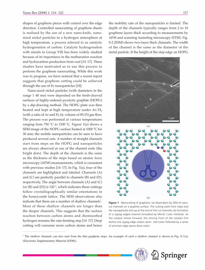
Nano-sized nickel particles (with diameters in the range 1 40 nm) were deposited on the fresh-cleaved surfaces of highly-ordered pyrolytic graphite (HOPG) by a dip-drawing method. The HOPG plate was then heated and kept at high temperature under Ar/H2 (with a ratio of Ar and H2 by volume of 85:15) gas fl ow. The process was performed at various temperatures ranging from 750 ºC to 1100 ºC. Figure 1(a) shows a SEM image of the HOPG surface heated at 1000 ºC for 30 min; the mobile nanoparticles can be seen to have produced several cuts. A number of straight channels start from steps on the HOPG and nanoparticles are always observed at one of the channel ends (the bright dots). The depth of the channels is the same as the thickness of the steps based on atomic force microscopy (AFM) measurements, which is consistent with previous studies [14 17]. In Fig. 1(a), four of the channels are highlighted and labeled. Channels (A) and (C) are perfectly parallel to channels (B) and (D), respectively. The angle between channels (A) and (C) (or (B) and (D)) is 120 º, which indicates these cuttings follow crystallographically similar orientations in the honeycomb lattice. The SEM observations also indicate that there are a number of shallow channels1. Most of these shallow channels are longer than the deeper channels. This suggests that the surface reaction between carbon atoms and chemisorbed hydrogen remains the rate-limiting step [14 17]. Deep cutting will consume more carbon atoms and hence
the mobility rate of the nanoparticles is limited. The depth of the channels typically ranges from 2 to 10 graphene layers thick according to measurements by AFM and scanning tunneling microscopy (STM). Fig. S-2 (ESM) shows two-layer thick channels. The width of the channel is the same as the diameter of the metal particle. If the height of the step edge on HOPG
1 The shallow channels can also start from the thin graphene steps. An example of such a shallow channel is shown in Fig. S-1(a)
(Electronic Supplementary Material (ESM)).
(a)
(b)
C
A
B
D
1 μm
Figure 1 Nanocutting of graphene: (a) observation by SEM of nano-cut channels on a graphite surface. The cutting starts from steps and the nanoparticles end up at the end of the cut channels; (b) formation of a zigzag edged channel simulated by Monte Carlo methods. As the catalyst moves forward, the moving front of the catalyst first etches one zigzag edge carbon atom (red color) followed by a series of armchair edge atoms (blue color)

118 Nano Res (2008) 1: 116 122
Nano Research
is larger than the particle size, the cut is buried under the top layer as the particle burrows through the sub-surface graphene layers.
Previous reports have indicated that Ni particles etch channels mainly along the [1120] direction
[15 17] with a small fraction along the [1100] direction [14]. Our SEM observations also show that most of the cuttings take place along one of these directions. However, as shown in Fig. 2(a), STM scanning reveals a number of very narrow channels (<10 nm), and most of these narrow channels show an orientation different from that seen for the wider ones. Atomically resolved STM images are used to determine the orientation of these channels relative to the lattice. Since it is diffi cult to directly acquire clear atomic resolved STM images on the edges, the directions of the channels were identified by referring to the crystallographic orientation of the top graphene layer adjacent to the channel. An example of such an atomic-resolution STM image is shown in Fig. 2(b). After taking a large-area image (Fig. 2(a)), the zoomed-in images with atomic resolution (Fig. 2(b)) near the channels were acquired immediately in order to avoid any adverse effect induced by thermal drift. It is interesting and important to note that all the channels with widths of ~10 nm or more are parallel to the graphene [1120] orientation, while nearly all the channels smaller
than ~10 nm follow the [1100] direction. Since the width of the channels is determined by the size of catalyst particles, this fi nding paves a way to control the types of the edges cut by precisely controlling the particle (knife) size.
The mechanism of catalytic hydrogenation of graphite is controversial [14, 15]. Previous observations that the reaction rate depends linearly on the surface area of the catalyst particle support the carbon dissolution mechanism. We performed density functional calculations using a PBE exchange-correlation functional with the Vienna Ab Initio Simulation Package (VASP) [19], the results of which supported this hypothesis (For modeling details, please see ESM). The calculations showed that on a Ni (111) surface, removal of one carbon atom from armchair and zigzag edges requires 0.518 eV and 1.852 eV, respectively. Thus, it is easier to dissolve carbon atoms from the armchair edge than
from the zigzag edge. Carbon atoms at graphene edges dissociate on the catalyst, and then react with hydrogen on its surface. The mechanism can be regarded as the reverse of catalytic carbon nanofi ber growth [20, 21]. We also performed kinetic Monte Carlo simulations in order to understand this effect. In our simulations, the nickel catalyst particle was modeled as a sphere placed in a graphene lattice or near a free graphene edge. The armchair or zigzag sites in contact with the catalyst particle were then
(a)
(b)Figure 2 Orientation of channels as determined by STM: (a) STM images showing nano-channels in various directions; (b) zoom-in image with atomic resolution showing the crystallographic orientation of graphene. The insert diagram illustrates the graphite crystal structure. Only every other surface carbon atom, as labeled by large black dots in the insert, appears as a protrusion in the STM image. The hexagonal units are also labeled. The atomically resolved STM image acquired at the area close to the channels exhibits a long-range waviness, which implies a modulation in the electronic structure induced by the channel edges
[1100]
[1120] [1120]
100 nm
[1100]
[1120]
600 pm

119Nano Res (2008) 1: 116 122
dissolved with probability1 PAM = 1 and PZZ = 0.1, respectively. The simulations showed that zigzag channels were formed in most cases after the catalytic etching (Fig. 1(b)). This is easy to understand because an armchair site will be etched away immediately after it is formed (PAM=1). The critical step in the forward motion of the catalyst is dissolving one carbon atom from the zigzag edge and forming armchair sites around the kink as illustrated in Fig. S-4(b) (ESM). However, for smaller particles, armchair channels can be formed after etching2, consistent with the experimental observations that most of the thinner
channels follow the [1100] direction.We also observed several turns for the channels
during cutting. All the angles for these turns are 120º (shown in Fig. 3(a)), or 60º. This indicates that the particles move, while cutting, along symmetric directions along the graphene lattice. It is noted that even after the channels turn (which could occur several times for a single channel), the edge structure remains the same (zigzag or armchair). Only few turns with a 90º angle were observed3. Monte Carlo simulations indicate that a metal particle prefers to keep to a straight channel when it is moving inside a graphene lattice. Turning along any direction will detach part of the catalyst surface from the graphene edge, and will decrease the adhesive energy. Our microscopic observations indicate that a free edge (either a graphene step or the edge of an existing channel) can easily cause the turning. When a particle approaches a free edge, if the channel is shallower than the edge thickness, it will be bounced back at an angle of 60º (more frequently) or 120º (in rare cases as shown later). This can be explained in terms of the strong binding between catalyst particle and graphene edges (for details, see ESM, Fig. S-5). The adhesive strength between the graphene edges
1 PAM stands for the dissolution probability of armchair edges, and PZZ the dissolution probability of zigzag edges.2 Using PAM =1 for armchair edge etching is based on the assumption that the dissolution of armchair sites is effi cient. Small particles are
assumed to be spherical (especially at higher temperatures), and the contact between their surface and graphene edges may not suffi cient,
and thus some armchair edges should remain after etching. To simulate this, we carried out modeling with a smaller dissolution
possibility (PAM) for armchair edge (PAM < 1). As shown in Fig. S-4(b) (ESM), an armchair edged channel forms in this scenario.3 The 90º turning means that movement of the particles changes in different crystallographic orientations. However, after the fi rst 90º
turn, the channel does not appear straight, and its edges are not very smooth (Fig. S-1(b), ESM), which indicates that this orientation is
not favorable for the particle size involved.
(b)
(a)
(c)Figure 3 Turning of channels along the symmetry lines: (a) channels with several 120º and 60º turnings; (b), (c) simulation results for catalyst particle approaching a free edge (b) and a void (c), where it makes a turn in order to minimize the adhesive energy between catalyst and graphene edges
120˚
60˚
120˚
120˚1 μm
Void
Free edge

120 Nano Res (2008) 1: 116 122
Nano Research
and nickel particles is calculated to be as high as 1 eV/Å [21]. When the catalyst reaches the free edges of a graphene step or a wider channel, considerable surface tension will pull it back and result in a 60º turn of the channel. Doing this will form a larger interface and reduce the energy (Fig. 3(b)). However, when approaching a very narrow channel, the catalyst can still have sufficient contact with both edges of the channel, making it is possible for it to make a 120º turn1. It is possible to create other defects (e.g., voids from vacancy clusters) on the surface of graphene by gasification reactions [22]. Our simulations indicate that such defects can also change the direction of a channel at 120º angles (Fig. 3(c)).
By controlling the factors that introduces turns while channel cutting, it is possible to achieve fabrication of specific graphene components for electronic applications. The scanning probe images in Figs. 4(a) (c) display different graphene pieces in various shapes obtained by the nano-cutting process. Based on the edge effect (metal particle getting bounced back at the edges), particle movement can be controlled. Figure 4(d) shows three basic cutting models (A), (B), and (C) based on the experimental observations in Figs. 4(a) (c). As shown in Fig. 4(a) (Model (A)), graphene ribbons in a parallelogram shape may be cut by particles moving parallel to an existing channel between two parallel channels.
(a)
(b)
(c)
(d)
[1120]60˚
60˚
60˚60˚
60˚
60˚60˚
60˚
[1120]
[1120]
[1100]
60˚ 120˚
Metal particle Graphene edge
1 μm
50 nm
[1100]
[1100]
500 nm
(A)
(B)
(C)
Figure 4 Experimental observations and basic designs for controlled cutting of graphene sheets: (a) AFM image of graphene ribbons with different sizes; (b) STM image of equilateral triangle shaped graphene formed by channels along the [1100] orientation; (c) AFM image showing a two layers thick graphene ribbon with [1100] edges (identifi ed by the direction of all the wider channels nearby) cut by one [1120] oriented channel; (d) Three cutting models based on the cuttings observed in (a), (b), and (c). Model (A): nanoparticle movement between two parallel channels forms a parallelogram shaped graphene ribbon. Model (B): nanoparticle moving between two parallel channels forms an equilateral triangle graphene shape. All the channels in Model (A) or (B) are along the same crystallographic orientation. Model (C): particle movement in a different crystallographic orientation from the edges forms graphene pieces in a right-angled triangle shape with one angle of 60º (60º turning) or in an isosceles triangle shape with one angle of 120º (120º turning)
1 An example of this is shown in Fig. S-1(c) (ESM).
Channel

121Nano Res (2008) 1: 116 122
Graphene ribbons formed by these wider channels should be zigzag edged. In Fig. 4(b) (Model (B)), a metal particle moving up and down between two
parallel channels along [1100] creates perfect armchair edged graphene pieces in an equilateral triangle shape1. In addition, we often observed the cutting seen in Model (C). As Fig. 4(c) shows, the edges of the
graphene ribbon are parallel to the [1100] direction. However, the cutting direction determined by the particle size is along the [1120] orientation. There are two turning possibilities when the particle is moving at an inclination of 30º to the edge: channel turning of 60º forms a right-angled triangle shape, and turning of 120º forms a graphene piece in an isosceles triangle shape. We note that the graphene triangle pieces formed here are composed of edges with different crystallographic orientations. Triangle shaped graphene pieces are thus a basic component that can be obtained by our cutting process. Recent theoretical investigations have indicated that zigzag-edged triangle graphene pieces could be a promising component in nanoscale spintronics, because the orientation of the triangular edges may break the symmetry between graphene sublattices, and lead to a large spin [10, 11]. Future electronic circuits may consist of patterned graphene components with different shapes and sizes cut from graphene sheets. For example, Figs. S-3(a), (b) show this kind of complicated cut. Using our process, coupled with future developments that could exactly position metal particles on graphene, it may be possible to achieve the goal of nanoscale graphene engineering. We used this approach to directly cut graphene fragments transferred on to Si substrates following the literature [18], and devices based on the cut structures are being fabricated and tested. It is also possible to cut epitaxially grown graphene on SiC wafers [23].
In summary, using a nanoparticle knife that can be chemically driven, cutting of graphene sheets into different ribbon and triangle shapes can be achieved. Experimental observations and theoretical analysis indicate that the cutting directions in the graphene planes can be controlled by the size of the metal particles, in principle allowing graphene pieces to be cut with discrete armchair or zigzag edges. These
1 Cutting between [1120] oriented channels or edges forms zigzag edged equilateral triangle graphene pieces, as shown in Fig. S-1(d) (ESM).
controllably cut graphene pieces may provide the basic testing components in future electronic applications.
Method
Ni nanoparticle deposition process: Ni nanoparticles were deposited on HOPG plates (Mikromasch ZYB grade) by a dip-drawing process. First, 0.2 mmol/L NiCl2/ethanol solution was prepared. HOPG plates with surfaces freshly cleaved by Scotch tape were immersed into the catalyst solution, and drawn out slowly so that the solution formed a uniform solution film on the HOPG surface. After drying, the HOPG pieces were annealed at 500 ºC in 1.3 slm (standard liters per minute) gas flow of Ar with 15 vol% H2 for 1 h, resulting in the formation of Ni nanoparticles on their surfaces. Following annealing at 500 ºC, the furnace was directly heated to the desired temperature using the same gas fl ow to start the cutting (hydrogenation process). After a certain duration (30 60 min), the furnace was cooled down to room temperature with gas protection.
Scanning electron microscopy (SEM) (FEI Quanta 400 ESEM FEG), atomic force microscopy (AFM) (Digital Instruments Nanoscope IIIA), and scanning tunneling microscopy (STM) were performed on the channels cut into the surface of the HOPG. STM measurements were performed in ultra high vacuum with an Omicron VT-STM system operated by RHK electronics. Topography images were acquired in the constant current mode of operation with a sample bias of 0.4 V and a tunneling current of 20 pA.
We performed density functional theory (DFT) calculations in order to understand the carbon dissolution mechanism. We carried out Monte Carlo simulations using different rates for armchair and zigzag edge etching. In the simulations, the graphene edged carbon atoms in contact with the metal catalyst were etched with a probability P=exp( E/kBT), which was calculated from the energy E required for etching and the environmental temperature T. After etching surrounding carbon atoms, the metal catalyst moves under the influence of the adhesive force to the graphene edges.

122 Nano Res (2008) 1: 116 122
Nano Research
Acknowledgements
The authors (P. M. Ajayan, L . Ci . , W. Gao) acknowledge support from the Interconnect Focus Center, one of fi ve research centers funded under the Focus Center Research Program, a Semiconductor Research Corporation program.
Electronic Supplementary Material: Additional SEM, AFM and STM images, snapshots from the Monte Carlo simulation, details of adhesive energy cost to change the cutting direction, modeling details, and a movie of the cutting process are available in the online version of this article at http://dx.doi.org/10.1007/s12274-008-8020-9 and is accessible free of charge.
References
[1] Novoselov, K. S.; Geim, A. K.; Morozov, S. V.; Jiang D.;
Zhang, Y.; Dubonos, S. V.; Grigorieva, I. V.; Firsov, A.
A. Electric field effect in atomically thin carbon films.
Science 2004, 306, 666 669.
[2] Novoselov, K. S.; Geim, A. K.; Morozov, S. V.; Jiang, D.,
Katsnelson, M. I.; Grigorieva, I. V.; Dubonos, S. V.; Firsov.
A. A. Two-dimensional gas of massless Dirac fermions in
graphene. Nature 2005, 438, 197 200.
[3] Zhang, Y.; Tan, J. W.; Stormer, H. L.; Kim, P. Experimental
observation of the quantum Hall effect and Berry’s phase
in graphene. Nature 2005, 438, 201 204.
[4] Morozov, S. V.; Novoselov, K. S.; Katsnelson, M. I.;
Schedin, F.; Ponomarenko, L. A.; Jiang, D.; Geim, A. K.
Strong suppression of weak localization in graphene.
Phys. Rev. Lett. 2006, 97, 016801.
[5] McCann, E.; Kechedzhi, K.; Fal’ko, V. I.; Suzuura,
H.; Ando, T.; Altshuler, B. L. Weak-local isat ion
magnetoresistance and valley symmetry in graphene.
Phys. Rev. Lett. 2006, 97, 146805.
[6] Van Noorden, R. Moving towards a graphene world.
Nature 2006, 442, 228 229.
[7] Kobayashi, Y.; Fukui, K.; Enoki, T.; Kusakabe, K.;
Kaburagi, Y. Observation of zigzag and armchair edges
of graphite using scanning tunneling microscopy and
spectroscopy. Phys. Rev. B 2005, 71, 193406.
[8] Son, Y.; Cohen, M. L.; Louie, S. G. Half-metallic graphene
nanoribbons. Nature 2006, 444, 347 349.
[9] Son, Y.; Cohen, M. L.; Louie, S. G. Energy gaps in graphene
nanoribbons. Phys. Rev. Lett. 2006, 97, 216803.
[10] Wang, W. L.; Meng, S.; Kaxiras, E. Graphene nanofl akes
with large spin. Nano Lett. 2008, 8, 241 245.
[11] Fernández-Rossier, J.; Palacios, J. J. Magnetism in
graphene nanoislands. Phys. Rev. Lett. 2007, 99, 177204.
[12] Schedin, F.; Geim, A. K.; Morozov, S. V.; Hill, E. W.;
Blake, P.; Katsnelson, M. I.; Novoselov, K. S. Detection
of individual gas molecules adsorbed on graphene. Nat.
Mater. 2007, 6, 652 655.
[13] Li, X.; Wang, X.; Zhang, L.; Lee, S.; Dai, H. Chemically
d e r i v e d , u l t r a s m o o t h g r a p h e n e n a n o r i b b o n
semiconductors. Science 2008, 319, 1229 1232.
[14] Tomita A.; Tamai, Y. An optical microscopic study on the
catalytic hydrogenation of graphite. J. Phys. Chem. 1974,
78, 2254 2258.
[15] Keep, C. W.; Terry, S.; Wells, M. Studies of the nickel-
catalyzed hydrogenation of graphite. J. Catal. 1980, 66,
451 462.
[16] Baker, R. T. K.; Sherwood, R. D.; Derouane, E. G. Further
studies of the nickel/graphite-hydrogen reaction. J. Catal.
1982, 75, 382 395.
[17] Goethel, P. J.; Yang, R. T. Mechanism of graphite
hydrogenation catalyzed by nickel. J. Catal. 1987, 108,
356 363.
[18] Datta, S. S.; Strachan, D. R.; Khamis, S. M.; Johnson, A. T.
C. Crystallographic etching of few-layer graphene. Nano
Lett. 2008, 8, 1912 1915.
[19] Kresse, G.; Joubert, D. From ultrasoft pseudopotentials
to the projector augmented-wave method. Phys. Rev. B
1999, 59, 1758 1775.
[20] Helveg, S.; López-Cartes, C.; Sehested, J.; Hansen, P. L.;
Clausen, B. S.; Rostrup-Nielsen, J. R.; Abild-Pedersen F.;
Nørskov, J. K. Atomic-scale imaging of carbon nanofi bre
growth. Nature 2004, 427, 426 429.
[21] Ding, F.; Larsson, P.; Larsson, J. A.; Ahuja, R.; Duan, H.;
Rosen A.; Bolton, K. The importance of strong carbon-
metal adhesion for catalytic nucleation of single-walled
carbon nanotubes. Nano Lett. 2008, 8, 463 468.
[22] Chang, H.; Bard, A. J. Scanning tunneling microscopy
studies of carbon-oxygen reactions on highly oriented
pyrolytic graphite. J. Am. Chem. Soc. 1991, 113, 5588
5596.
[23] Berger, C.; Song, Z.; Li, T.; Li, X.; Ogbazghi, A. Y.; Feng,
R.; Dai, Z.; Marchenkov, A. N.; Conrad, E. H.; First, P. N.;
de Heer, W. A. Ultrathin epitaxial graphite: 2D electron
gas properties and a route toward graphene-based
nanoelectronics. J. Phys. Chem. B 2004, 108, 19912
19916.


![Optical Spectroscopic Studies of Photochemically Oxidized ...[4] Endo M, Strano M S and Ajayan P M 2008 Carbon Nanotubes: Advanced Topics in the Synthesis, Structure, Properties and](https://img.dokumen.tips/doc/110x75/5f92c4bf52dae24bd057c062/optical-spectroscopic-studies-of-photochemically-oxidized-4-endo-m-strano.jpg)


![[A] Non-Maharashtra Students · [A] Non-Maharashtra Students ... 23 101804 ABHANA AJAYAN SREEDHARAN AJAYAN OPEN 85 ... 89 97911 RIDDHI DEEPAK BHAT OPEN 85.2](https://img.dokumen.tips/doc/110x75/5ad4398b7f8b9a075a8b65a1/a-non-maharashtra-a-non-maharashtra-students-23-101804-abhana-ajayan-sreedharan.jpg)