Embed Size (px)
Citation preview
Control of Secondary Electron Emission Flux through
Surface Geometry
Research Review Seminar
February 9, 2018
Charles Swanson
1
Introduction
2
• The phenomenon of Secondary Electron Emission (SEE)
• Modeling considerations
• Practical applications
• The phenomenon of SEE suppression by surface geometry
• Candidate geometries
• Tungsten fuzz in tokamak divertors
• Other industrial applications for these surfaces
• The tool: Monte-Carlo simulation
• Our work:
• Velvet
• Feathers
• Fuzz/foam
• Conclusions
• References

The phenomenon of Secondary Electron Emission
(SEE)
3
High-energy electrons collide with electrons in a
surface. Some are able to escape.
Secondary Electron Yield (SEY) follows a universal
curve, usually tabulated empirically. Shown is that of
Scholtz, Philips J. Res. (1996) [1]. Figure from
Sydorenko, PhD thesis (2006) [2]
Secondary Electron flux is made of “true” secondaries
(approximately Maxwellian), “rediffused” secondaries
(approximately uniform in energy), and “reflected”
secondaries (same energy as primary). Figure from
Sydorenko, PhD thesis (2006) [2]
SEY can be
above unity
Rediffused
secondaries
Reflected
secondaries
True secondaries
Primary electron
Primary electron
Secondary
electron
Secondary
electron
Secondary electrons are emitted with flux weighted in the
normal direction, 𝑃 Ω = cos𝜃
Bronstein, Vtorichnaya Elektronnaya Emissiya (1969) [3]

Modeling considerations
4
SEE can alter potential profiles. Strong SEE can
make sheaths literally disappear. Sim. B is with
net Secondary Electron Yield (SEY) of 1.
Campanell, Phys Rev Lett (2012) [4]
SEE from a very biased electrode can inject fast
electrons which penetrate deep into your system,
ruining your fluid model. Kushner, IEEE Trans.
Plasma Science (1986) [5]
Secondary
electrons
Secondary
electrons
SEE is ubiquitous. It occurs whenever plasma touches a surface. Sheath-heated secondary electrons may alter ionization
profiles, or secondaries may eliminate sheaths entirely.
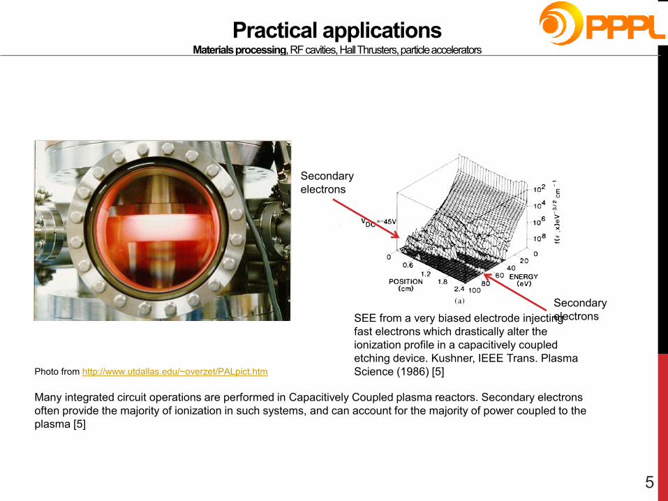
Practical applications Materials processing, RF cavities, Hall Thrusters, particle accelerators
5
SEE from a very biased electrode injecting
fast electrons which drastically alter the
ionization profile in a capacitively coupled
etching device. Kushner, IEEE Trans. Plasma
Science (1986) [5] Photo from http://www.utdallas.edu/~overzet/PALpict.htm
Many integrated circuit operations are performed in Capacitively Coupled plasma reactors. Secondary electrons
often provide the majority of ionization in such systems, and can account for the majority of power coupled to the
plasma [5]
Secondary
electrons
Secondary
electrons

Practical applications Materials processing, RF cavities, Hall Thrusters, particle accelerators
6
Multipactor effect limiting efficiency in an RF cavity.
Figure from Vaughan, IEEE Trans. Electron Devices
(1988) [6]
By Bukvoed - Own work, CC BY-SA 3.0,
https://commons.wikimedia.org/w/index.php?curid=4840831
RF cavities and amplifiers can have their total throughput limited by the Multipactor effect, a condition of secondary
electron amplification [6]

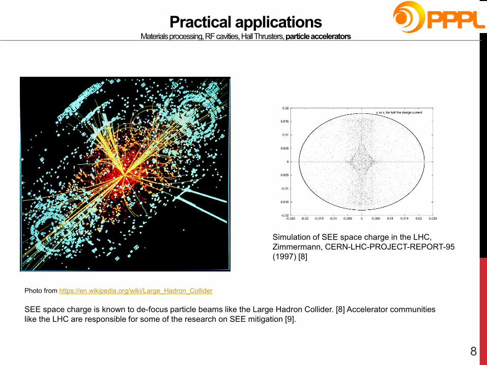
Practical applications Materials processing, RF cavities, Hall Thrusters, particle accelerators
7
Figure from Kaganovich et. al., Phys.
Plasmas (2007) [7]
Photo from https://en.wikipedia.org/wiki/Hall-effect_thruster
In a Hall Thruster, Ion current produces thrust while electron current is useless. Electron current is impeded
magnetically.
SEE can cause electron current in a Hall Thruster by allowing secondary electrons to migrate down the walls [7]
E
B
Practical applications Materials processing, RF cavities, Hall Thrusters, particle accelerators
8
Simulation of SEE space charge in the LHC,
Zimmermann, CERN-LHC-PROJECT-REPORT-95
(1997) [8]
Photo from https://en.wikipedia.org/wiki/Large_Hadron_Collider
SEE space charge is known to de-focus particle beams like the Large Hadron Collider. [8] Accelerator communities
like the LHC are responsible for some of the research on SEE mitigation [9].
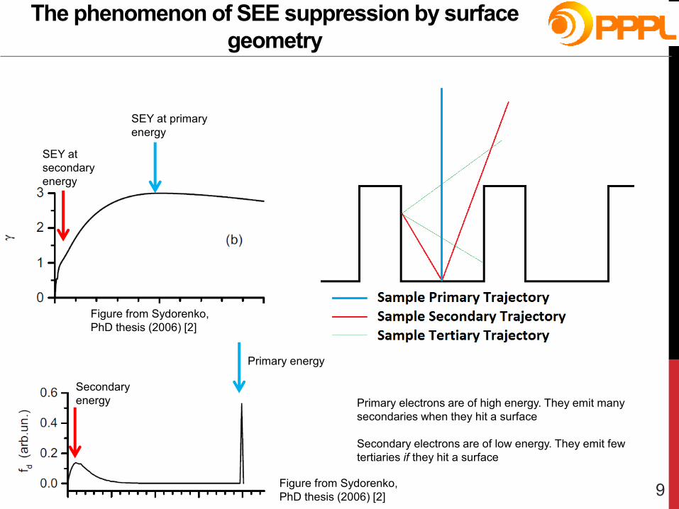
The phenomenon of SEE suppression by surface
geometry
9
Primary electrons are of high energy. They emit many
secondaries when they hit a surface
Secondary electrons are of low energy. They emit few
tertiaries if they hit a surface
Figure from Sydorenko,
PhD thesis (2006) [2]
Figure from Sydorenko,
PhD thesis (2006) [2]
SEY at primary
energy
SEY at
secondary
energy
Primary energy
Secondary
energy

Candidate geometries
10
Electron micrograph of “dendritic” copper. Figure
from Baglin et. al., Proceedings of EPAC 2000,
(2000) [10]
Schematic representation of triangular and
rectangular grooves. Figure from Pivi et. al., J. Appl.
Phys. (2008) [9]
Mix and matching of geometries: Micro-pores
floored by triangular grooves. Figure from Ye et. al.,
J. Appl. Phys. (2017) [11]
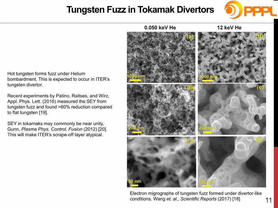
Tungsten Fuzz in Tokamak Divertors
11 Electron migrographs of tungsten fuzz formed under divertor-like
conditions. Wang et. al., Scientific Reports (2017) [18]
Hot tungsten forms fuzz under Helium
bombardment. This is expected to occur in ITER’s
tungsten divertor.
Recent experiments by Patino, Raitses, and Wirz,
Appl. Phys. Lett. (2016) measured the SEY from
tungsten fuzz and found >60% reduction compared
to flat tungsten [19].
SEY in tokamaks may commonly be near unity,
Gunn, Plasma Phys. Control. Fusion (2012) [20].
This will make ITER’s scrape-off layer atypical.

Other Industrial Applications for these surfaces
12
Fibrous and fractal-like surfaces are being developed anyway in industry for a variety of applications
http://www.ultramet.com/
Aerospace companies produce micro- architectured materials for improved thermal resistivity or increased emittance.
At right is a radiatively-cooled rocket firing.
Many chemical catalysts have fractal
shapes. Figure from Ramos et. al.
Scientific Reports (2017) [21]

The tool: Monte-Carlo simulation
13
Empirical Model at surface:
𝛾 𝐸𝑝, 𝜃 = 𝛾𝑚𝑎𝑥 𝜃 × exp −ln
𝐸𝑝𝐸𝑚𝑎𝑥 𝜃
2 𝜎
2
𝛾𝑚𝑎𝑥 𝜃 = 𝛾0 1 +𝑘𝑠𝜃
2
2𝜋
𝐸𝑚𝑎𝑥 𝜃 = 𝐸0(1 +𝑘𝑠𝜃
2
𝜋)
Graphite: 𝛾0 = 1.2, 𝐸0 = 325𝑒𝑉, 𝜎 = 1.6, 𝑘𝑠 = 1
𝑓𝑒𝑙 𝐸𝑝 = exp 1.59 + 3.75 ln 𝐸𝑝 − 1.37 ln 𝐸𝑝2+ 0.12 ln 𝐸𝑝
3
Adapted from references [1],[12],[13]
Surfaces implemented as iso-surfaces
Number of particles: 105
Swanson, J. Appl. Phys. (2016) [14]

Our work: Velvet Swanson and Kaganovich , J. Appl. Phys.(2016) [14]
14
Velvet: regular or irregular lattice of normally-
oriented fibers Lines: Analytic model.
Points: Monte-Carlo simulations.
Discrepancy is due to tertiary and higher-order
electrons.
Velvet is well-suited to suppressing normally
incident primary electrons

Our work: Velvet Swanson and Kaganovich , J. Appl. Phys. (2016) [14]
15
Analytic model approximation:
Probability of whisker intersection is
constant per length traveled
perpendicular to whisker axis:
𝑃 Δ𝑧 = 𝑒−𝑢Δ𝑧tan𝜃1/ℎ
𝑢 =𝜋
2𝐷𝐴 = 2𝑟𝑛ℎ
𝑢 dimensionless parameter, 𝐷 area packing fraction, 𝐴 aspect ratio of fibers, 𝑟
radius of fibers, 𝑛 area density of fibers, ℎ height of fiber layer
P 𝑒 : Probability of escape into the bulk
𝛾𝑒𝑓𝑓 = 𝛾 × P 𝑒 𝑡𝑜𝑝 P 𝑧ℎ𝑖𝑡 = ℎ + P 𝑒 𝑏𝑜𝑡𝑡𝑜𝑚 P 𝑧ℎ𝑖𝑡 = 0 + ∫ 𝑑𝑧P 𝑒 𝑧 P 𝑧
1 × 𝐷 (1 − 𝐷)𝑒−𝑢tan𝜃1× 2∫ 𝑑𝑡𝑡𝑒−𝑢𝑡
1 + 𝑡2 2
2
𝜋1 − 𝐷 tan𝜃1 × ∫ 𝑑𝑡
𝑡2
1 + 𝑡2 2
1 − 𝑒−𝑢(𝑡+tan𝜃1)
𝑡 + tan𝜃1
(a 𝑧 integration has already been carried out)
This term dominates in a long, thin velvet
𝑡 = tan𝜃2

Recent experiment: Velvet Jin, Ottaviano, and Raitses , J. Appl. Phys. (2017) [15]
16
Experimental SEY values for a real carbon velvet. The pink
velvet had nominal values: 𝐷 = 0.035, 𝐴 = 430, 𝑢 = 24. This
measured SEY is a ~65% reduction.
“81%” corresponds to the amount of area as seen from perfectly
normal whose view of the substrate is obstructed, a slightly
different definition from ours.
Disagreement with experiment could be due to a distribution of
axial alignments, rather than the perfectly normal assumed by
Swanson & Kaganovich (2016) [14].
Furthermore, our model assumed 𝛾 ∝ 1 +𝑘𝑠𝜃
2
2𝜋, while this paper
claims that a 𝛾 ∝ 1/ cos 𝜃 relationship is more accurate. Further
work is needed to resolve this discrepancy.
Jin, Ottaviano, and Raitses
performed measurements of
surfaces with velvet fibers.

Our work: Feathers Swanson and Kaganovich , J. Appl. Phys. (2017) [16]
17 Feather: lattice of normally-oriented fibers with smaller,
secondary fibers on the sides of that fiber.
Solid lines: Simulation.
Dashed lines: Numerical Velvet (“primary whisker”)
result.
“Side SEY half”: The SEY from the sides of the
whisker is reduced by a factor of 2.
u=4: This SEY trace is that of primary whiskers
which are thicker than the primary whisker
simulated.
Note that secondary whisker suppress beyond
what infinitely long primary whiskers are able to.
Rather than observing, we designed a shape that could out-
perform other shapes at suppressing SEE. Our shape is two
scales of velvet.

Our work: Fuzz/foam Swanson and Kaganovich , J. Appl. Phys. (2018) [17]
18
Fuzz/foam: irregular lattice of isotropically-
oriented fibers
Lines: Analytic model.
Points: Monte-Carlo simulations.
Discrepancy is due to tertiary and higher-order
electrons.
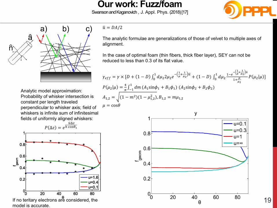
19
Analytic model approximation:
Probability of whisker intersection is
constant per length traveled
perpendicular to whisker axis; field of
whiskers is infinite sum of infinitesimal
fields of uniformly aligned whiskers:
𝑃 Δ𝑧 = 𝑒 𝑢 Δ𝑧
ℎ cos𝜃1
𝑢 = 𝐷𝐴/2
The analytic formulae are generalizations of those of velvet to multiple axes of
alignment.
In the case of optimal foam (thin fibers, thick fiber layer), SEY can not be
reduced to less than 0.3 of its flat value.
𝛾𝑒𝑓𝑓 = 𝛾 × [𝐷 + 1 − 𝐷 ∫ 𝑑𝜇22𝜇2𝑒−
1
𝜇+
1
𝜇2𝑢 1
0+ (1 − 𝐷) ∫ 𝑑𝜇2
1−𝑒−
1𝜇+
1𝜇2
𝑢
1+𝜇
𝜇2
𝑃 𝜇2 𝜇1
0]
𝑃 𝜇2 𝜇 =4
𝜋∫ 𝑑𝑚1
−1(𝐴1sin𝜙1 + 𝐵1𝜙1) (𝐴2sin𝜙2 + 𝐵2𝜙2)
𝐴1,2 = (1 −𝑚2)(1 − 𝜇1,22 ), 𝐵1,2 = 𝑚𝜇1,2
𝜇 = cos𝜃
Our work: Fuzz/foam Swanson and Kaganovich , J. Appl. Phys. (2018) [17]
If no teritary electrons are considered, the
model is accurate.

Conclusions
20
• Control over secondary electron emission has theoretical and practical
implications
• In recent years, an avenue for such control has been complex surface
geometry
• Such surface geometries can be evaluated by Monte-Carlo simulations before
being experimentally measured
• Fibrous surfaces, which are developed for other purposes, are well-suited to
secondary electron suppression

Bibliography
21
[1] J. Scholtz et al., “Secondary electron emission properties,” Philips J. Res. 50, 375 (1996).
[2] Sydorenko, Dmytro. “Particle-in-Cell Simulations of Electron Dynamics in Low Pressure Discharges with Magnetic Fields,” 2006.
https://ecommons.usask.ca/handle/10388/etd-06142006-111353.
[3] Vtorichnaya Elektronnaya Emissiya, edited by I. M. Bronstein and B. S. Fraiman (Nauka, Movkva, 1969), p. 340 (in Russian).
[4] Campanell, M. D., A. V. Khrabrov, and I. D. Kaganovich. “Absence of Debye Sheaths Due to Secondary Electron Emission.” Physical
Review Letters 108, no. 25 (June 18, 2012): 255001.
[5] Kushner, M. J. “Mechanisms for Power Deposition in Ar/SiH4 Capacitively Coupled RF Discharges.” IEEE Transactions on Plasma
Science 14, no. 2 (April 1986): 188–96. https://doi.org/10.1109/TPS.1986.4316522.
[6] J. R. M. Vaughan, “Multipactor,” IEEE Trans. Electron Devices 35, 1172–1180 (1988).
[7] I. Kaganovich, Y. Raitses, D. Sydorenko, and A. Smolyakov, “Kinetic effects in a Hall thruster discharge,” Phys. Plasmas, vol. 14, no. 5,
p. 057104, May 2007.
[8] Zimmermann, Frank. “A Simulation Study of Electron Cloud Instability and Beam Induced Multipacting in the LHC,” 1997.
[9] M. T. F. Pivi et al., “Sharp reduction of the secondary electron emission yield from grooved surfaces,” J. Appl. Phys. 104, 104904
(2008).
[10] V. Baglin, J. Bojko, O. Grabner, B. Henrist, N. Hilleret, C. Scheuerlein, and M. Taborelli, “The secondary electron yield of technical
materials and its variation with surface treatments,” in Proceedings of EPAC 2000, 26–30 June 2000, Austria Center, Vienna, pp. 217–221.
[11] M. Ye, W. Dan, and H. Yongning, “Mechanism of total electron emission yield reduction using a micro-porous surface,” J. Appl. Phys.
121(12), 124901 (2017).
[12] J. Vaughan, “A new formula for secondary emission yield,” IEEE Trans. Electron Devices 36, 1963 (1989).
[13] M. Patino, Y. Raitses, B. Koel, and R. Wirz, “Application of Auger spectroscopy for measurement of secondary electron emission from
conducting material for electric propulsion devices,” in 33rd International Electric Propulsion Conference (IPEC), The George Washington
University, Washington, DC, USA, 6–10 October 2013.
[14] Swanson, Charles, and Igor D. Kaganovich. “Modeling of Reduced Effective Secondary Electron Emission Yield from a Velvet
Surface.” Journal of Applied Physics 120, no. 21 (December 7, 2016): 213302. https://doi.org/10.1063/1.4971337.
[15] Jin, Chenggang, Angelica Ottaviano, and Yevgeny Raitses. “Secondary Electron Emission Yield from High Aspect Ratio Carbon
Velvet Surfaces.” Journal of Applied Physics 122, no. 17 (November 1, 2017): 173301. https://doi.org/10.1063/1.4993979.
[16] Swanson, Charles, and Igor D. Kaganovich. “‘Feathered’ Fractal Surfaces to Minimize Secondary Electron Emission for a Wide Range
of Incident Angles.” Journal of Applied Physics 122, no. 4 (July 24, 2017): 043301. https://doi.org/10.1063/1.4995535
[17] Swanson, Charles, and Igor D. Kaganovich. “Modeling of Reduced Secondary Electron Emission Yield from a Foam or Fuzz Surface.”
Journal of Applied Physics 123, no. 2 (January 10, 2018): 023302. https://doi.org/10.1063/1.5008261.
[18] Wang, Kun, R. P. Doerner, M. J. Baldwin, F. W. Meyer, M. E. Bannister, Amith Darbal, Robert Stroud, and Chad M. Parish.
“Morphologies of Tungsten Nanotendrils Grown under Helium Exposure.” Scientific Reports 7 (February 14, 2017): 42315.
https://doi.org/10.1038/srep42315.
[19] M. Patino , Y. Raitses , and R. Wirz , “ Secondary electron emission from plasma-generated nanostructured tungsten fuzz,” Appl.
Phys. Lett. 109(20), 201602 (2016). https://doi.org/10.1063/1.4967830
[20] Gunn J P 2012 Plasma Phys. Control. Fusion 54 085007
[21] Ramos, Manuel, Félix Galindo-Hernández, Ilke Arslan, Toby Sanders, and José Manuel Domínguez. “Electron Tomography and
Fractal Aspects of MoS 2 and MoS 2 /Co Spheres.” Scientific Reports 7, no. 1 (September 26, 2017): 12322.
https://doi.org/10.1038/s41598-017-12029-8.


![A Herschel Galactic Plane Survey of [NII] Emission: Preliminary Results Paul F. Goldsmith Umut Yildiz William D. Langer Jorge L. Pineda Jet Propulsion](https://img.dokumen.tips/doc/110x75/56649d775503460f94a589e1/a-herschel-galactic-plane-survey-of-nii-emission-preliminary-results-paul.jpg)