Embed Size (px)
Citation preview

Contains copyrighted material.
Do not distribute
Lecture 9: Embedded DSP Processor Papers
Embedded Computing Systems
Michael Schulte

Papers M. J. Schulte, J. Glossner, S. Jinturkar, M.
Moudgill, S. Mamidi, and S. Vassiliadis, "A Low-Power Multithreaded Processor for Software Defined Radio," Journal of VLSI Signal Processing Systems, vol. 43, No. 2/3, pp. 143-159, June 2006.
M. Woh, S. Seo, S. Mahlke, T. Mudge, C. Chakrabarti, and K. Flautner, “AnySP: Anytime Anywhere Anyway Signal Processing,” Proceedings of the 36th International Symposium on Computer Architecture, pp. 128-139, June 2009.

The Sandblaster™ Processor
High Parallelism Multiple operations per cycle SIMD vector operations Thread-level parallelism Multiple processors per chip
Data Memory64KB
8-Banks
Data Memory64KB
8-Banks
Data Memory64KB
8-Banks
Data Memory64KB
8-Banks
Data Memory64KB
8-Banks
Data Memory64KB
8-Banks
Data Memory64KB
8-Banks
Data Memory64KB
8-Banks
I-Cache64KB
64B Lines4W (2-Active)
I-Cache64KB
64B Lines4W (2-Active)
I-Cache64KB
64B Lines4W (2-Active)
I-Cache64KB
64B Lines4W (2-Active)
I-Decode
DIRLRU Replace
Bus/Memory Interface
Instruction Fetch and Branch Unit
Integer and Load/Store Unit
SIMD Vector UnitSIMD Vector UnitSIMD Vector UnitSIMD Vector Unit

High-Performance Compound Instructions Example
L0: lvu %vr0,%r3,8|| vmulreds %ac0,%vr0,%vr0,%ac0|| loop %lc0,L0
load vector update: 4 16-bit loads + address update vector multiply and reduce: 4 16-bit saturating multiplies + 4 32-
bit saturating adds loop: decrement, compare against zero and branch
Throughput 3 complex operations/cycle 16 RISC-ops/cycle 4 MACS/cycle
20 tap finite impulse response (FIR) filter 3.92 MACs/cycle sustained ~16 RISC-ops/cycle sustained

Vector Processing Unit (VPU)
- VPEs use SIMD execution to process 4 elements each instr.
- Shuffle unit supports data transfers between VPEs
- Reduction unit and accumulator register file work with VPEs to provide fast dot products
Accumulator Data
Load Data
Store Data
VPE0
Shuffle Unit
Reduction Unit
Accumulator Register File
VPE2
VPE1
VPE3
Store Data
Load Data
VPEn
Shuffle Data Out
Shuffle Data In
Reduction Unit Data
VPE Interface
64-bit Load Bus
64-bit Store Bus

Vector Operations
Most vector operation are performed on four sets of vector elements in SIMD fashion.
Vector operands are 8, 16, 32, or 40 bits.
A0 A1 A2 A3
B0 B1 B2 B3
A0+B0 A1+B1 A2+B2 A3+B3
va
vb
wt
VPE0 VPE1 VPE2 VPE3

Vector Multiply-Reduce-Add A vector multiply-reduce-add operation computes
A variation of this instruction performs saturation after each operation Results outside the range of [-1, +1) are saturated Facilitates high-performance dot product operations Required for certain cellphone standards
A0 A1 A2 A3
B0 B1 B2 B3
va
vb
Cwa
C+A0·B0+A1·B1+A2·B2 +A3·B3wt

SandBlaster Pipelines
All register files have just two read ports and one write port Staggered read and write-back stages Banked register files for even-odd threads Different operations write to different register files
Long latency instructions Allows high clock rates at low voltages Time to access slower memory Hidden by multithreaded hardware
0 1 2 3 4 5 6 7 8 9 10 Ld/St Inst
Dec RF
Read Agen Xfer Int.
Ext Mem
0 Mem
1 Mem
2 RFWB
ALU Inst Dec
Wait RF Read
Exec1 Exec2 Xfer RFWB
I_Mul Inst Dec
Wait RF Read
Exec1 Exec2 Exec3 Xfer RFWB
V_Mul Inst Dec
VRF Read
MPY1 MPY2 Add1 Add2 Xfer VRFWB
V_Mul Reduce
Inst Dec
VRF Read
MPY1 MPY2 Add1 Add2 ARF Rd
Reduce 1
Reduce 2
Reduce 3
Reduce 4
ARFWB

Multithreaded Execution
PC0
PC1
PC2
PC3
Program Counters
GPR0
GPR1
GPR2
GPR3
GPR31
Shared GPRs
VR0
VR1
VR2
VR3
VR31
Shared VRs
01:lw gr1,10(gr2)02:add gr3,gr2,gr103:cmp cr1,gr2,gr3
11:add gr3,gr3,gr312:lvu vr3,20(gr3)13:vadd vr4,vr1,vr3
Thread0: PC = PC0CR = CR0registers 0 to 7
21:add gr1,gr2,gr322:lhu gr2,15(gr1)23:shl gr4,gr2,sh
31:lv vr1,18(gr2)32:vsub vr3,vr2,vr1 33:vmul vr6,vr1,vr3
Thread2: PC = PC2CR=CR2 registers 16 to 24
Thread1: PC = PC1CR = CR1 registers 8 to 15
Thread3: PC = PC3CR= CR3registers 24 to 31
CR0
CR1
CR2
CR3
Shared CRs
• The Sandblaster DSP simultaneous supports up to eight hardware threads
• Each thread has its own storage, but threads share functional units

Multithreading in SDR Multithreading is works well for SDR
Block level pipelining Exploit data level parallelism in communication
algorithms Provide a platform for distribution of real-time and
non-real time workloads
T0, T1, T3, T4
T5 T6, T7 T8 T9 T10
OFDMInner
DecoderInner De-interleaver
Outer Decoder
Outer De-interleaver
2K or 8K FFTBit-Wise De-Puncturing Operations
64-state Viterbi Decoder
Reed-Solomon Decoder, Galois-Field Arithmetic
De-randomizer
Bit-Wise XOR and Shift Operations
High BW Byte Select Operations
To MPEG Decoder
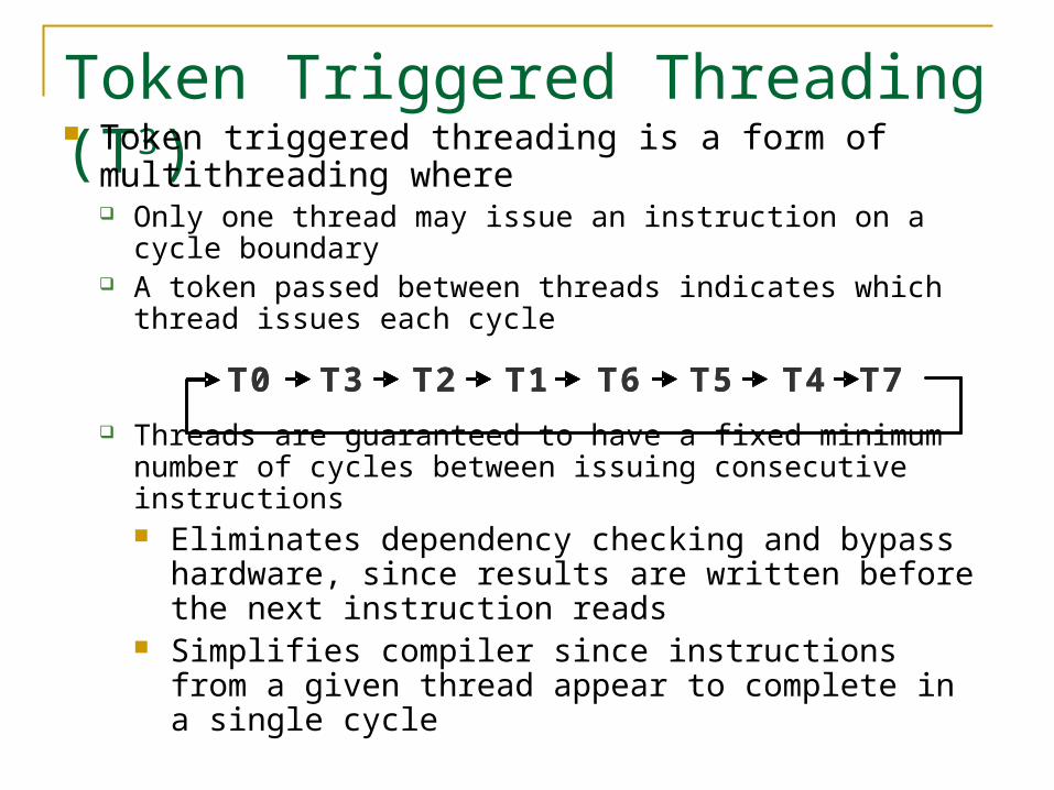
Token Triggered Threading (T3) Token triggered threading is a form of multithreading
where Only one thread may issue an instruction on a cycle
boundary A token passed between threads indicates which thread
issues each cycle
Threads are guaranteed to have a fixed minimum number of cycles between issuing consecutive instructions Eliminates dependency checking and bypass
hardware, since results are written before the next instruction reads
Simplifies compiler since instructions from a given thread appear to complete in a single cycle
T0 T3 T5T2 T1 T6 T4 T7T0 T3 T5T2 T1 T6 T4 T7

Multithreaded Pipeline Consecutive instructions from the same
thread do not cause pipeline stalls.
vmul %vr0, %vr1, %vr2vand %vr3, %vr4, %vr0
Inst.Dec.
VRFRead
Mpy1 Mpy2 Add1 Add2 XFer VRFWB
Inst.Dec.
VRFRead
vmul
vand
instructions from other threads
cycle 1 2 3 4 5 6 7 8 9 10

GeneralPurpose I/O
SB3010 Handset Chip
Smart CardInterface
Sync SerialPort
KeyboardInterface
KeypadInterface
UART/IrDA
AudioCodec
Interface
GeneralPurpose I/O
Timers
RTC
MultimediaCard
Interface
32.768KHz
Multi PortMemory
Controller
USBInterface
LCDInterface
AHB APBBridge
PeripheralDevice Control
DMAController
ARM922TProcessor
Vector InterruptController
DSP ARMBridge
DSP
Ins & Data Mem(64KB / 64KB)
L2 M
em(256K
B)
EX
T IN
T
DSP
Ins & Data Mem(64KB / 64KB)
L2 M
em(256K
B)
EX
T IN
T
DSP
Ins & Data Mem(64KB / 64KB)
L2 M
em(256K
B)
EX
T IN
T
DSP
Ins & Data Mem(64KB / 64KB)
L2 M
em(256K
B)
EX
T IN
T
DSP Complex
GeneralPurpose I/O
SerialInterfaces(SPI, I2C)
ParallelStreaming
DataInterface
Prog.Timers/Gens
Clock Generation
10 – 50MHz REF
REF1 REF2Ext. clks
Int. clks...
DSP Local Peripherals TAP(JTAG Port)
RX Data
TX Data
Timer I/O
RF Control
Memory Interface(Synchronous and
Asynchronous)
0.13um CMOS
Replicated SB core
Low power design

SB3010 Communications Results
0
10
20
30
40
50
60
70
80
90
100
1/2/
5.5/
11M
bps
Class 1
0/12
64k /
384
k / 2
M
% S
B30
10 U
tili
zati
on
75m
.5se
c xy
z
5m
.1se
c xy
z
4x60
0MH
z
2.9
Mbp
s
144k
bps /
1.2
Mbp
s
S-Vide
o

Performance vs. Power – Processor CoresDSP Performance vs. Power
(Log-Log Scale)
1
10
100
1000
10000
100000
1 10 100 1000mWatts
MM
AC
/s
Sandblaster
C55x SC110
SC140
SC110
C54x
C55x
C64xSC140
MSA
1M/mW
5M/mW
5M/mW
10M/mW
10M/mW
1M/mW
50M/mW
50M/mW

Questions What types of parallelism are available in the
Sandblaster Processor? Why is multithreading useful in wireless
communication applications? What advantages and disadvantages does
Token Triggered Threading have compared to Simultaneous Multithreading?
What are some potential limitations of the Sandblaster Architecture

AnySP: Anytime Anywhere Anyway Signal ProcessingMark Woh1, Sangwon Seo1, Scott Mahlke1,Trevor Mudge1, Chaitali Chakrabarti2, Krisztian Flautner3
University of Michigan – ACAL1
Arizona State University2
ARM, Ltd.3
Portions of these slides have been modified for use in ECE902.Do not distribute.

Cost for Multi-System Support
Supporting multiple systems is reserved for the most expensive phones Cost is in supporting all the systems that may or may not be used at once
19
Programmable Unified Architectures Provide
Lower Cost Faster Time to Market Support for Multiple Applications (Current and Future) Bug Fixes After Manufacturing
So where do we start?

Power/Performance Requirements for Multiple Systems
20
Different applications have different power/performance characteristics!
We need to design keeping each application in mind!
(Not GPP but Domain Specific Processor)
1
10
100
1000
10000
0.1 1 10 100
Better
Pow
er Efficiency
1 Mops/mW
10 Mops/mW100 Mops/mW
1000 Mops/mW
SODA(65nm)
SODA (90nm)
TI C6X
Imagine
VIRAM Pentium M
IBM Cell
Pe
rfo
rma
nce
(G
op
s)
Power (Watts)
3G Wireless
4G Wireless
Mobile HDVideo
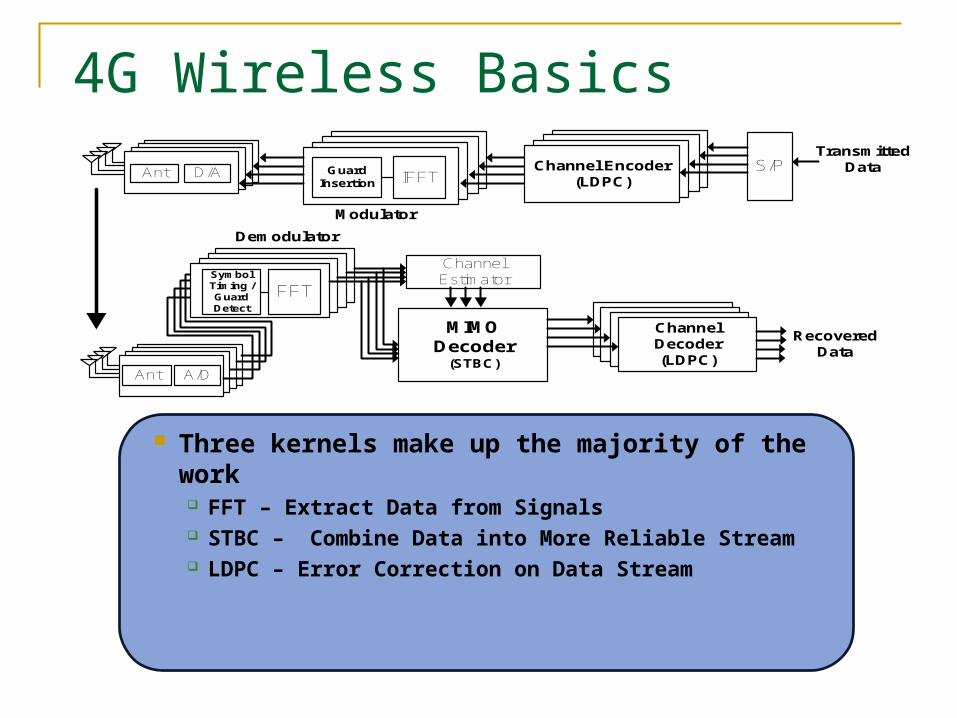
4G Wireless Basics
Three kernels make up the majority of the work FFT – Extract Data from Signals STBC – Combine Data into More Reliable Stream LDPC – Error Correction on Data Stream
21
Ant A/D
FFTSymbol Timing / Guard Detect
Channel Estimator
MIMODecoder
(STBC)
Channel Decoder(LDPC)
Recovered Data
Ant D/A IFFTGuard Insertion
Channel Encoder(LDPC)
S/PTransmitted
Data
Modulator
Demodulator

Mobile Signal Processing Algorithm Characteristics
22
Algorithms have different SIMD widths From very large to very small
Though SIMD width varies all algorithms can exploit it Large percentage of work can use SIMD
Larger SIMD width tend to have less TLP
SIMD comes at a cost!•Register File Power
•Data Movement/Alignment CostSIMD architectures have to deal with this!
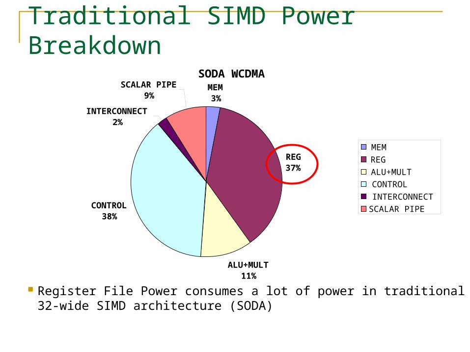
Traditional SIMD Power Breakdown
Register File Power consumes a lot of power in traditional 32-wide SIMD architecture (SODA)
SODA WCDMAMEM3%
REG37%
ALU+MULT11%
CONTROL38%
INTERCONNECT2%
SCALAR PIPE9%
MEM
REG
ALU+MULT
CONTROL
INTERCONNECT
SCALAR PIPE

Register File Access
24
Many of the register file access do not have to go back to the main register file
Lots of power wasted on unneeded register file access!

Instruction Pair Frequency
25
Like the Multiply-Accumulate (MAC) instruction there is opportunity to fuse other instructions
A few instruction pairs (3-5) make up the majority of all instruction pairs!
a) Intra- prediction and Deblocking Filter Combined
Instruction Pair Frequency1 multiply-add 26.71%2 add-add 13.74%3 shuffle-add 8.54%4 shift right-add 6.90%5 subtract-add 6.94%6 add-shift right 5.76%7 multiply-subtract 4.00%8 shift right-subtract 3.75%9 add-subtract 3.07%
10 Others 20.45%
b) LDPC
Instruction Pair Frequency1 shuffle-move 32.07%2 abs-subtract 8.54%3 move-subtract 8.54%4 shuffle-subtract 3.54%5 add-shuffle 3.54%6 Others 43.77%
c) FFT
Instruction Pair Frequency1 shuffle-shuffle 16.67%2 add-multiply 16.67%3 multiply-subtract 16.67%4 multiply-add 16.67%5 subtract-mult 16.67%6 shuffle-add 16.67%

Data Alignment Problem!
H.264 Intra-prediction has 9 different prediction modes Each prediction mode requires a specific permutation
26
B C D
A B C D B C D A B C D A B C D
A B C D
A A A A B B B B C C C C D D D D
A B C D
A B C D B C D C
E
E D E
F G
GF D E F
A
A B C D E F G H I J
A B C D G H I JG H I J A B C D
A B C D E F G
A
A B C D E F G H I J
A B C D E F G H I J
A B C D E F G H I J
K L
K L
A B B C C D DD D D DE F F G G
CDE EF FG GHI J JK KLI
CE F G H I J KI J K L D E FD
F F FEG G HH I D E G C D E F0 1 2 3
4 5 6 7
8 9 10 11
12 13 14 15
16
164
4
16x16 luma MBprediction modes for each 4x4 block
a b c d
e f g h
i j k l
m n o p
I
J
K
L
A B C DX
Traditional SIMD machines take too long or cost too much to do this
Good news – small fixed number patterns per kernel
Intra-Prediction

Summary
Conclusion about 4G and H.264 Lots of different sized parallelism
From 4 wide to 96 wide to 1024 wide SIMD Which means many different SIMD widths need to be
supported
Very short lived values Lots of potential for instruction fusings Limited set of shuffle patterns required for each
kernel

Traditional SIMD Architectures
28
32-laneSIMDALU
SIMDRF
32-laneSSN
SIMDto
scalar
EX
WB
STV
VTS
scalarRF
16-bitALU
EX
WB
SIMDDataMEM
ScalarDataMEM
SIMD
Scalar
AGU
32-Wide SIMD with Simple Shuffle Network

CROSSBAR
Scalar Pipeline
Bank 0
Bank 1
Bank 2
Bank 15
L1ProgramMemory
Controller
Bank 3
Bank 4
16-bit 8-wide 16 entry
SIMD RF-0
16-bit 8-wide 16 entry
SIMD RF-1
16-bit 8-wide 16 entry
SIMD RF-2
16-bit 8-wide 16 entry
SIMD RF-7
Scalar Memory Buffer
Multi-SIMD Datapath
AGU Group 0 Pipeline
AGU Group 7 Pipeline
AGU Group 1 Pipeline
Multi-Bank Local Memory
DMA
To Inter-PE
Bus
8 Groups of 8-wide
SIMD(64 Total Lanes)
8-wide SIMD FFU-0
8-wide SIMDFFU-1
8-wide SIMDFFU-2
8-wide SIMD FFU-7
SwizzleNetwork
16-bit 8-wide 4-entry
Buffer-0
16-bit 8-wide 4-entry
Buffer-1
16-bit 8-wide 4-entry
Buffer-2
16-bit 8-wide 4-entry
Buffer-7
Multi-Output Adder Tree
AnySP PE
AnySP Architecture – High Level
8 Groups of 8-Wide Flexible Function
Units
128x128 16bit Swizzle Network
16 Banked Memory with SRAM-based Crossbar
Multiple Output Adder Tree
Temporary Buffer and Bypass Network
Datapath AGU and Scalar Pipeline

Multi-Width Support
30
16-bit 8-wide 16 entry
SIMD RF-0
16-bit 8-wide 16 entry
SIMD RF-1
16-bit 8-wide 16 entry
SIMD RF-2
16-bit 8-wide 16 entry
SIMD RF-7
Multi-SIMD Datapath
AGU Group 0
AGU Group 7
AGU Group 1
8-wide SIMD FFU-0
8-wide SIMDFFU-1
8-wide SIMDFFU-2
8-wide SIMD FFU-7
SwizzleNetwork
16-bit 8-wide 4-entry
Buffer-0
16-bit 8-wide 4-entry
Buffer-1
16-bit 8-wide 4-entry
Buffer-2
16-bit 8-wide 4-entry
Buffer-7
Multi-Output Adder Tree
CROSSBAR
Bank 0
Bank 1
Bank 2
Bank 15
Bank 3
Bank 4
Multi-Bank Local Memory
16-bit 8-wide 16 entry
SIMD RF-3
8-wide SIMDFFU-3
16-bit 8-wide 4-entry
Buffer-3
AGU Group 2
AGU Group 3
Normal 64-Wide SIMD mode – all lanes share one AGU
16-bit 8-wide 16 entry
SIMD RF-0
16-bit 8-wide 16 entry
SIMD RF-1
16-bit 8-wide 16 entry
SIMD RF-2
16-bit 8-wide 16 entry
SIMD RF-7
Multi-SIMD Datapath
AGU Group 0
AGU Group 7
AGU Group 1
8-wide SIMD FFU-0
8-wide SIMDFFU-1
8-wide SIMDFFU-2
8-wide SIMD FFU-7
SwizzleNetwork
16-bit 8-wide 4-entry
Buffer-0
16-bit 8-wide 4-entry
Buffer-1
16-bit 8-wide 4-entry
Buffer-2
16-bit 8-wide 4-entry
Buffer-7
Multi-Output Adder Tree
CROSSBAR
Bank 0
Bank 1
Bank 2
Bank 15
Bank 3
Bank 4
Multi-Bank Local Memory
16-bit 8-wide 16 entry
SIMD RF-3
8-wide SIMDFFU-3
16-bit 8-wide 4-entry
Buffer-3
AGU Group 2
AGU Group 3
16-bit 8-wide 16 entry
SIMD RF-0
16-bit 8-wide 16 entry
SIMD RF-1
16-bit 8-wide 16 entry
SIMD RF-2
16-bit 8-wide 16 entry
SIMD RF-7
Multi-SIMD Datapath
AGU Group 0
AGU Group 7
AGU Group 1
8-wide SIMD FFU-0
8-wide SIMDFFU-1
8-wide SIMDFFU-2
8-wide SIMD FFU-7
SwizzleNetwork
16-bit 8-wide 4-entry
Buffer-0
16-bit 8-wide 4-entry
Buffer-1
16-bit 8-wide 4-entry
Buffer-2
16-bit 8-wide 4-entry
Buffer-7
Multi-Output Adder Tree
CROSSBAR
Bank 0
Bank 1
Bank 2
Bank 15
Bank 3
Bank 4
Multi-Bank Local Memory
16-bit 8-wide 16 entry
SIMD RF-3
8-wide SIMDFFU-3
16-bit 8-wide 4-entry
Buffer-3
AGU Group 2
AGU Group 3
Each 8-wide SIMD Group works on different memory locations of the same 8-wide code – AGU Offsets

AnySP FFU Datapath
Flexible Functional Unit allows us to
1.Exploit Pipeline-parallelism by joining two lanes together2.Handle register bypass and the temporary buffer3.Join multiple pipelines to process deeper subgraphs4.Fuse Instruction Pairs

Simulation Environment
Traditional SIMD architecture comparison SODA at 90nm technology
AnySP Synthesized at 90nm TSMC Power, timing, area numbers were extracted
Performance and power for each kernel were generated using synthesized data on in-house simulator
32

AnySP Speedup vs SIMD-based Architecture
For all benchmarks AnySP performs more than 2x better than a SIMD-based architecture
33
0.0
0.5
1.0
1.5
2.0
2.5Baseline 64-Wide Multi -SIMD Swizzle Network Flexible Functional Unit Buffer + Bypass
No
rma
lized
Sp
eed
up
FFT 1024ptRadix-2
FFT 1024ptRadix-4
STBC LDPC H.264Intra
Prediction
H.264Deblocking
Filter
H.264Inverse
Transform
H.264Motion
Compensation

AnySP Energy-Delay vs SIMD-based Architecture
More importantly energy efficiency is much better!
34
0.0
0.2
0.4
0.6
0.8
1.0
No
rma
lize
d E
ne
rgy
-De
lay SIMD- based Architecture AnySP
FFT 1024ptRadix-2
FFT 1024ptRadix-4
STBC LDPC H.264Intra
Prediction
H.264Deblocking
Filter
H.264Inverse
Transform
H.264Motion
Compenstation

PE
System
Total
Components Units
SIMD Data Mem (32KB)SIMD Register File (16x1024bit)SIMD ALUs, Multipliers, and SSN
SIMD Pipeline+Clock+Routing
Intra-processor InterconnectScalar/AGU Pipeline & Misc.
ARM (Cortex-M3)Global Scratchpad Memory (128KB)
Inter-processor Bus with DMA
90nm (1V @300MHz)
4444
44
111
AreaAreamm2
Area%
9.76 38.78%3.17 12.59%4.50 17.88%1.18 4.69%
0.94 3.73%1.22 4.85%
0.6 2.38%1.8 7.15%1.0 3.97%
25.17 100%
Est.65nm (0.9V @ 300MHz) 13.1445nm (0.8V @ 300MHz) 6.86
4G + H.264 DecoderPower
mWPower
%
102.88 7.24%299.00 21.05%448.51 31.58%233.60 16.45%
93.44 6.58%134.32 9.46%
2.5 <1%10 <1%
1.5 <1%
1347.03 100%
1091.09862.09
SIMD Buffer (128B)SIMD Adder Tree
44
0.82 3.25%0.18 <1%
84.09 5.92%10.43 <1%
AnySP Power Breakdown
Estimates indicate that both H.264 and 4G wireless can be done in under 1 Watt at 45nm
35

Questions What are some key characteristics of wireless
communication and HD video algorithms? What aspects of AnySP are designed to
exploit these characteristics? How does the AnySP architecture differ from
the Sandblaster architecture? What are some potential limitations of the
AnySP architecture?