Embed Size (px)
Citation preview
EVGA Z87 FTW Motherboard
1
Configuring the Z87 FTW BIOS
This supplementary manual explains the different menus and selections within the BIOS and
provides a description of the different options enabling you to configure the Z87 FTW BIOS for
your needs.
1. Entering BIOS 2
2. Header and Margin Information 3
3. Overclock 6
4. Memory 20
5. Advanced 31
6. Boot 65
7. Save and Exit 71
EVGA Z87 FTW Motherboard
2
Enter the BIOS
The Z87 FTW features a UEFI BIOS, allowing for full mouse and keyboard support to
streamline configuration. The BIOS enables you to use the base configuration of the
motherboard to set preferences for features and configure the board to perform optimally.
Follow the basic steps below to enter your BIOS.
1. Power on the computer.
2. Press the Del / Delete key when the message “Press Del to enter BIOS” appears on
screen.
a. In some instances, the Z87 FTW can complete the POST sequence before the
video card fully initializes and prevent you from seeing the POST screen and
the prompt for entering the BIOS, which may cause you to miss the
opportunity to enter the BIOS. In these instances, please repeatedly press
the Del/Delete button for a few seconds following the power on.
The Z87 FTW has 2 separate BIOS’s, toggled via the BIOS select switch. EVGA STRONGLY
recommends that you leave at least one BIOS unmodified to ensure that you have a failsafe
point that allows you to boot is an error occurs.
EVGA Z87 FTW Motherboard
3
Header and Margin
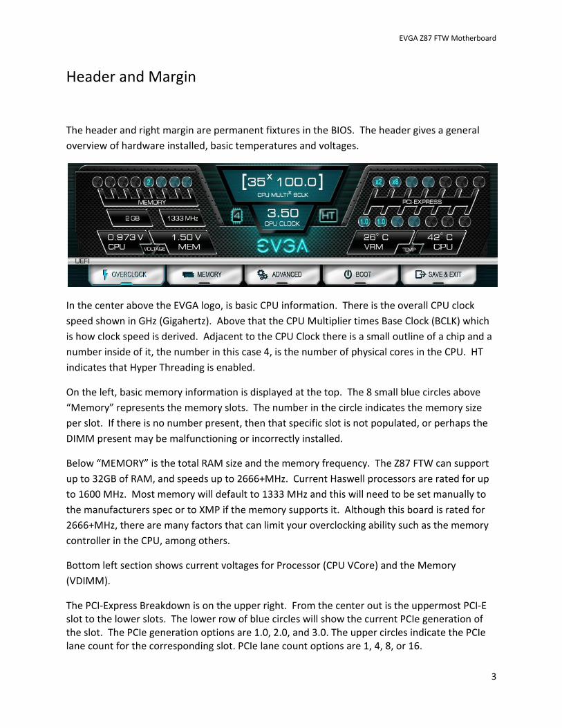
The header and right margin are permanent fixtures in the BIOS. The header gives a general
overview of hardware installed, basic temperatures and voltages.
In the center above the EVGA logo, is basic CPU information. There is the overall CPU clock
speed shown in GHz (Gigahertz). Above that the CPU Multiplier times Base Clock (BCLK) which
is how clock speed is derived. Adjacent to the CPU Clock there is a small outline of a chip and a
number inside of it, the number in this case 4, is the number of physical cores in the CPU. HT
indicates that Hyper Threading is enabled.
On the left, basic memory information is displayed at the top. The 8 small blue circles above
“Memory” represents the memory slots. The number in the circle indicates the memory size
per slot. If there is no number present, then that specific slot is not populated, or perhaps the
DIMM present may be malfunctioning or incorrectly installed.
Below “MEMORY” is the total RAM size and the memory frequency. The Z87 FTW can support
up to 32GB of RAM, and speeds up to 2666+MHz. Current Haswell processors are rated for up
to 1600 MHz. Most memory will default to 1333 MHz and this will need to be set manually to
the manufacturers spec or to XMP if the memory supports it. Although this board is rated for
2666+MHz, there are many factors that can limit your overclocking ability such as the memory
controller in the CPU, among others.
Bottom left section shows current voltages for Processor (CPU VCore) and the Memory
(VDIMM).
The PCI-Express Breakdown is on the upper right. From the center out is the uppermost PCI-E
slot to the lower slots. The lower row of blue circles will show the current PCIe generation of
the slot. The PCIe generation options are 1.0, 2.0, and 3.0. The upper circles indicate the PCIe
lane count for the corresponding slot. PCIe lane count options are 1, 4, 8, or 16.
EVGA Z87 FTW Motherboard
4
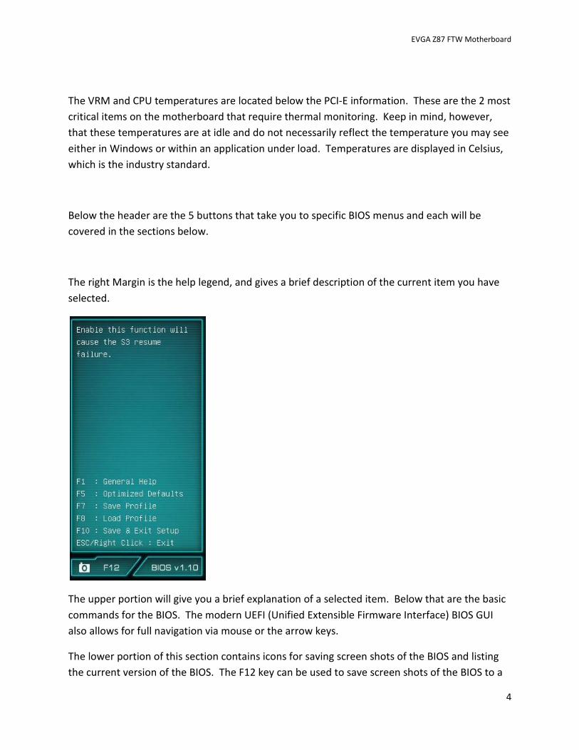
The VRM and CPU temperatures are located below the PCI-E information. These are the 2 most
critical items on the motherboard that require thermal monitoring. Keep in mind, however,
that these temperatures are at idle and do not necessarily reflect the temperature you may see
either in Windows or within an application under load. Temperatures are displayed in Celsius,
which is the industry standard.
Below the header are the 5 buttons that take you to specific BIOS menus and each will be
covered in the sections below.
The right Margin is the help legend, and gives a brief description of the current item you have
selected.
The upper portion will give you a brief explanation of a selected item. Below that are the basic
commands for the BIOS. The modern UEFI (Unified Extensible Firmware Interface) BIOS GUI
also allows for full navigation via mouse or the arrow keys.
The lower portion of this section contains icons for saving screen shots of the BIOS and listing
the current version of the BIOS. The F12 key can be used to save screen shots of the BIOS to a

EVGA Z87 FTW Motherboard
5
USB storage drive. To use this feature, a pre-formatted thumb drive must be plugged into one
of the USB headers, and then press F12 and a .bmp image will be saved to the thumb drives
root folder. This may be used to easily share BIOS configurations, or to visually back up settings
prior to doing a BIOS update to quickly and easily set original values back into the BIOS after the
flash is completed.
The BIOS version listed is the current version flashed of the ROM image, and will automatically
update every time the new BIOS is flashed.
Reference for the different bullet points:
• Setting
� Sub menu
� Preset Configurations (like XMP)
EVGA Z87 FTW Motherboard
6
Overclock
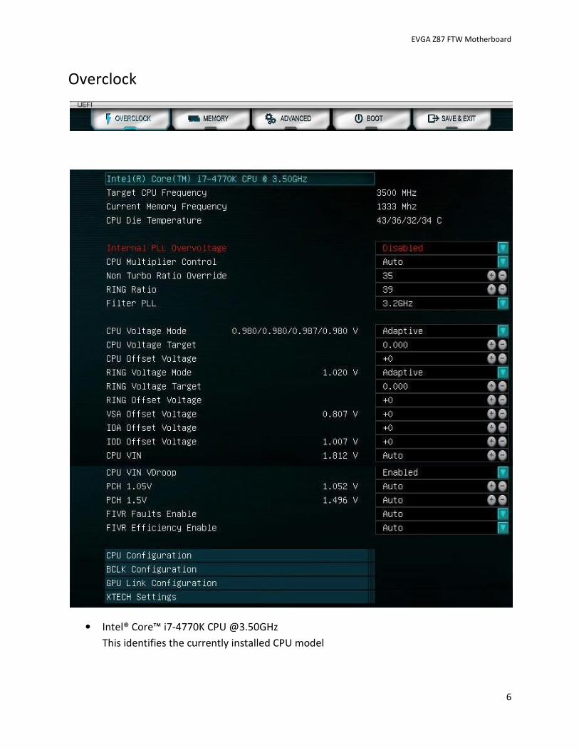
• Intel® Core™ i7-4770K CPU @3.50GHz
This identifies the currently installed CPU model
EVGA Z87 FTW Motherboard
7
• Target CPU Frequency
The product of the BCLK and the Multiplier: (BCLK Frequency * BCLK Ratio) * CPU
Multiplier = CPU Frequency.
• Current Memory Frequency
Displays the speed the memory is currently running at.
• CPU Die Temperature
This will display the temp of the individual cores.
• Internal PLL (Phased Locked Loop) Override
Enable/Disable
Enhanced clock management for extreme overclocking. Typically this is only used to
stabilize very high CPU Overclocks. S3 resume may not work properly if this is enabled
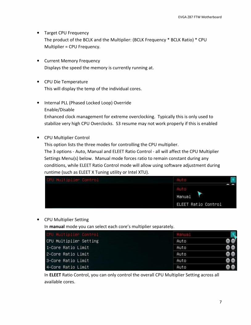
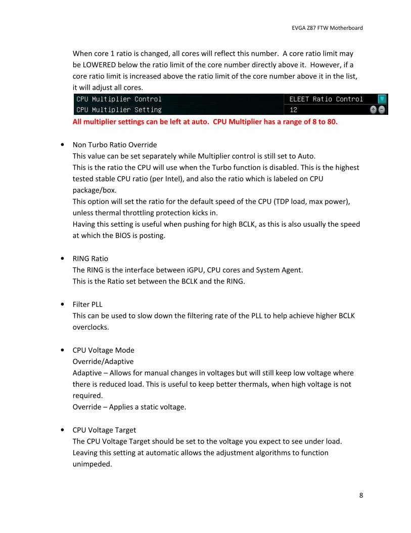
• CPU Multiplier Control
This option lists the three modes for controlling the CPU multiplier.
The 3 options - Auto, Manual and ELEET Ratio Control - all will affect the CPU Multiplier
Settings Menu(s) below. Manual mode forces ratio to remain constant during any
conditions, while ELEET Ratio Control mode will allow using software adjustment during
runtime (such as ELEET X Tuning utility or Intel XTU).
• CPU Multiplier Setting
In manual mode you can select each core’s multiplier separately.
In ELEET Ratio Control, you can only control the overall CPU Multiplier Setting across all
available cores.
EVGA Z87 FTW Motherboard
8
When core 1 ratio is changed, all cores will reflect this number. A core ratio limit may
be LOWERED below the ratio limit of the core number directly above it. However, if a
core ratio limit is increased above the ratio limit of the core number above it in the list,
it will adjust all cores.
All multiplier settings can be left at auto. CPU Multiplier has a range of 8 to 80.
• Non Turbo Ratio Override
This value can be set separately while Multiplier control is still set to Auto.
This is the ratio the CPU will use when the Turbo function is disabled. This is the highest
tested stable CPU ratio (per Intel), and also the ratio which is labeled on CPU
package/box.
This option will set the ratio for the default speed of the CPU (TDP load, max power),
unless thermal throttling protection kicks in.
Having this setting is useful when pushing for high BCLK, as this is also usually the speed
at which the BIOS is posting.
• RING Ratio
The RING is the interface between iGPU, CPU cores and System Agent.
This is the Ratio set between the BCLK and the RING.
• Filter PLL
This can be used to slow down the filtering rate of the PLL to help achieve higher BCLK
overclocks.
• CPU Voltage Mode
Override/Adaptive
Adaptive – Allows for manual changes in voltages but will still keep low voltage where
there is reduced load. This is useful to keep better thermals, when high voltage is not
required.
Override – Applies a static voltage.
• CPU Voltage Target
The CPU Voltage Target should be set to the voltage you expect to see under load.
Leaving this setting at automatic allows the adjustment algorithms to function
unimpeded.

EVGA Z87 FTW Motherboard
9
• CPU Offset Voltage
Offset is a static value which adds/reduces fixed voltage to achieve your desired voltage.
For example if we set the target to 1300mV, auto-adjustment will try to keep 1300mV
under load if power/thermals allow that. However, if the Target cannot properly auto-
adjust the voltage, Offset Voltage can be applied to make up the difference.
• RING Voltage Mode
Override/Adaptive
o Adaptive - Allows for manual changes in voltages but will still keep low voltage
where there is reduced load. This is useful to keep better thermals, when high
voltage is not required.
o Override will leave the voltage value static based on your adjustment.
• RING Voltage Target
The RING Voltage Target should be set to the voltage you expect to see under load.
Leaving this setting at automatic allows the adjustment algorithms to function
unimpeded.
• RING Offset Voltage
Offset is a static value which adds/reduces fixed voltage to achieve your desired voltage.
For example if we set the target to 1300mV, auto-adjustment will try to keep 1300mV
under load if power/thermals allow that. However, if the Target cannot properly auto-
adjust the voltage, Offset Voltage can be applied to make up the difference.
• VSA Offset Voltage
Voltage System Agent
VSA Offset Voltage increases the voltage threshold of the CPU Integrated memory
controller (IMC) and system control unit (SCU) voltage. High memory speeds over
2666mhz or BCLK overclocking may require an increasing in this voltage. Auto will adjust
voltage depending on memory frequency, or the values may be entered manually or by
scrolling through the options with the +/- keys.
• IOA Offset Voltage
Input/Output Analog
Increasing this voltage may help overclocking memory/pushing BCLK. Some CPUs may
be unstable if this voltage is set too low or too high.
• IOD Offset Voltage
EVGA Z87 FTW Motherboard
10
Input/Output Digital
Increasing this voltage may help overclocking memory/pushing BCLK. Some CPUs may
be unstable if this voltage is set too low or too high.
• CPU VIN
CPU Voltage Input
This is the only CPU VRM located on the motherboard’s PCB not controlled by the FIVR.
This voltage must be at least 0.4-0.6V higher than the set FIVR voltage. For example, if
the CPU Core voltage is set to 1.5V for extreme OC, VIN voltage must be set to at least
2.1V. Higher voltage will cause higher temperatures for the CPU, the increase in CPU VIN
will reduce the efficiency of the voltage regulation.
• CPU VIN Droop
Enable/Disable
This enables or disables Intel Spec VDroop functions for the CPU VIN. This may help to
get better stability when overclocking over 4.5GHz.
• PCH 1.05V
Platform Controller Hub
PCH serves as a south bridge for modern Intel Chipsets
1.1v is the base voltage core for the PCH core domain.
• PCH 1.5V
Platform Controller Hub
PCH serves as a south bridge for modern Intel Chipsets
1.5v adjustments control the voltage for the PCH I/O and the IVR (Input Voltage Range).
• FIVR Faults Enable
Fully Integrated Voltage Regulator
Auto/Enable/Disable
Intel FIVR power fault protection system. It is recommended to disable this protection
mechanism when doing extreme overclocking.
• FIVR Efficiency Enable
Fully Integrated Voltage Regulator
Auto/Enable/Disable
Efficiency optimized operation mode for Intel FIVR. This may cause instability during
extreme overclocking if enabled.
EVGA Z87 FTW Motherboard
11
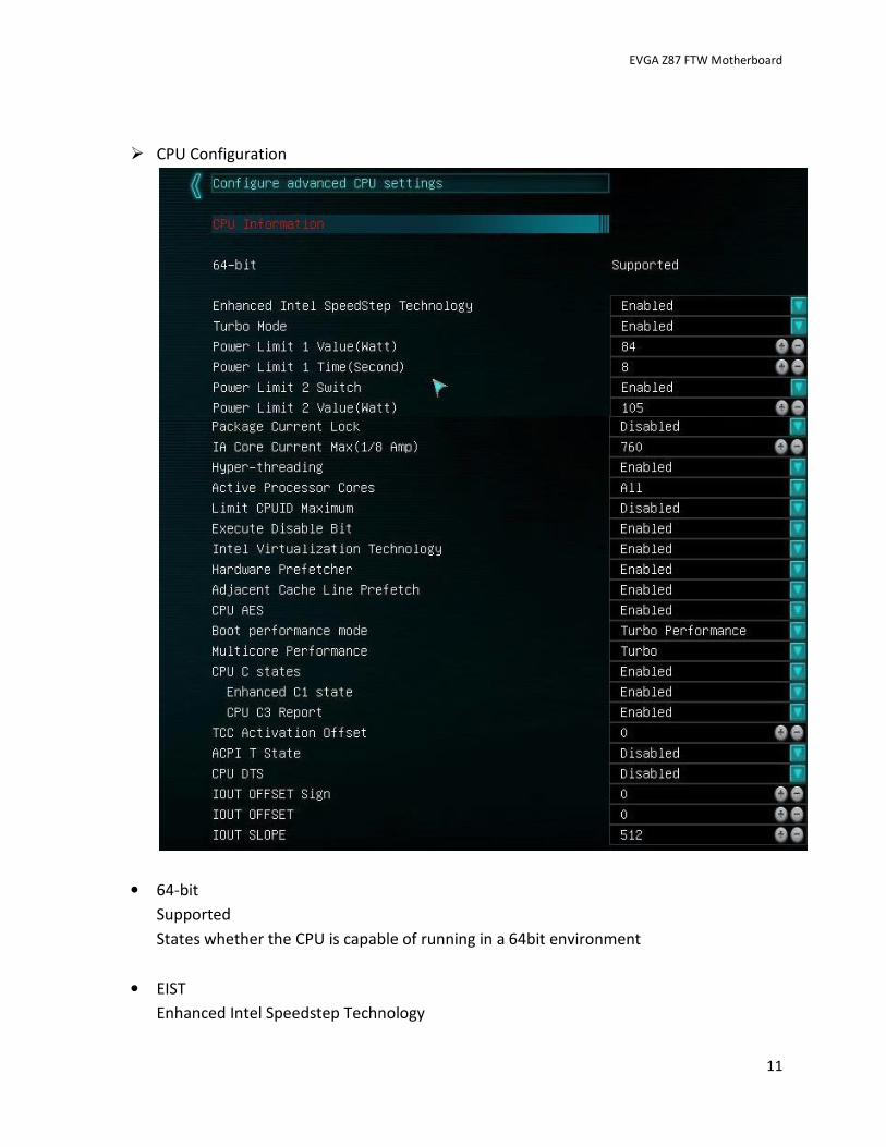
� CPU Configuration
• 64-bit
Supported
States whether the CPU is capable of running in a 64bit environment
• EIST
Enhanced Intel Speedstep Technology
EVGA Z87 FTW Motherboard
12
Enable/Disable
EIST allows the system to dynamically adjust processor voltage and core frequency,
which can result in decreased average power consumption and decreased average heat
production, based on the level of processor load.
• Turbo Mode
Enable/Disable
Turbo Mode allows the CPU to dynamically adjust frequency to accommodate higher
than average processor load to maintain peak performance. (In essence, low level
overclocking built into the CPU).
Power Limit information should always be defaulted to the Intel reference specs, they
can be adjusted if you are overclocking.
• Power Limit 1 Value (Watt)
Baseline Power Limit based off of CPU’s TDP.
• Power Limit 1 Time (Second)
If CPU passes the PL1 Value for more than the amount of seconds stated, the CPU will
throttle.
• Power Limit 2 Switch
Enable/Disable
A threshold or cap that if exceed, the PL2 rapid power limiting algorithms will attempt to
limit the spike above PL2.
• Power Limit 2 Value (Watt)
Peak Power limit, usually a value of 1.25 times the PL1 Wattage
• Package Current Lock
Enable/Disable
This is a limiter to prevent current on the whole package, either CPU or GPU, from going
over the preset value. This item needs to be unlocked/disabled to go any value over the
default spec.
• IA Core Current Max (1/8Amp)
Intel Architecture
(Value entered manually)
EVGA Z87 FTW Motherboard
13
This is the upper end current max for the CPU under load. When this is exceeded, the
CPU with throttle. The increase is done in 1/8th
amp increments. For example, a value
of 11 (11/8) would be 1.375 amps or 1 3/8th
• Hyper-threading
Enable/Disable
Hyper threading is processor core virtualization and functions as additional processing
cores for some applications. This setting is responsible for why a quad core processor
shows up as 8 threads in Windows.
• Active Processor Cores
This setting allows the selection of the number of processor cores to enable and make
available for use.
• Limit CPUID Maximum
When enabled, this sets the CPUID value to 03h, which assists with using Hyper
threaded CPUs in older operating systems that do not natively support Hyper Threading.
• Execute Disable Bit
Hardware-based security feature for protection against malicious software.
• Intel Virtualization Technology
Hardware based virtualization built into the CPU, used in conjunction with virtualization
software to create multiple virtual environments/virtual PC’s within a single PC.
• Hardware Prefetcher
The hardware prefetcher operates transparently, without programmer intervention, to fetch
streams of data and instruction from memory into the unified second-level cache. The
prefetcher is capable of handling multiple streams in either the forward or backward direction.
It is triggered when successive cache misses occur in the last-level cache and a stride in the
access pattern is detected, such as in the case of loop iterations that access array elements.
• Adjacent Cache Line Prefetch
The Adjacent Cache-Line Prefetch mechanism, like automatic hardware prefetch,
operates without programmer intervention. When enabled through the BIOS, two 64-
byte cache lines are fetched into a 128-byte sector, regardless of whether the additional
cache line has been requested or not. In applications with relatively poor spatial locality,
the cache miss ratio is higher.
EVGA Z87 FTW Motherboard
14
• CPU AES (Advanced Encryption Standard)
Enable/Disable
Advanced Encryption Standard Instruction Set is an extension to the x86 instruction set
architecture for microprocessors. The purpose of the instruction set is to improve the
speed of applications performing encryption and decryption.
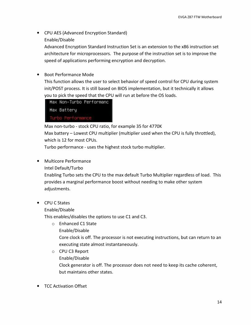
• Boot Performance Mode
This function allows the user to select behavior of speed control for CPU during system
init/POST process. It is still based on BIOS implementation, but it technically it allows
you to pick the speed that the CPU will run at before the OS loads.
Max non-turbo - stock CPU ratio, for example 35 for 4770K
Max battery – Lowest CPU multiplier (multiplier used when the CPU is fully throttled),
which is 12 for most CPUs.
Turbo performance - uses the highest stock turbo multiplier.
• Multicore Performance
Intel Default/Turbo
Enabling Turbo sets the CPU to the max default Turbo Multiplier regardless of load. This
provides a marginal performance boost without needing to make other system
adjustments.
• CPU C States
Enable/Disable
This enables/disables the options to use C1 and C3.
o Enhanced C1 State
Enable/Disable
Core clock is off. The processor is not executing instructions, but can return to an
executing state almost instantaneously.
o CPU C3 Report
Enable/Disable
Clock generator is off. The processor does not need to keep its cache coherent,
but maintains other states.
• TCC Activation Offset
EVGA Z87 FTW Motherboard
15
Thermal Control Circuitry
This is an offset in Celsius to reduce the thermal throttling point of the CPU. This is
secondary to the ACPI passive throttling of Turbo Mode.
• ACPI T State
(Advance Configuration and Power Interface)
T-state support enables the CPU driver to receive _TPC change notifications as a manner
of controlling the processor speed. This is frequently done on some systems as a passive
cooling mechanism along with the existing CPU ACPI P-States.
• CPU DTS Digital Thermal Sensor
Individual cores on die thermal sensor, this can report temperatures instantaneously.
THE BELOW IOUT SETTINGS ARE NORMALLY NOT ADJUSTED, BUT ARE THERE FOR
INCREASED FLEXIBILITY.
• IOUT Offset Sign
0/1
This is a setting for the FIVR current feedback; this will adjust the power circuit to enable
either earlier or later. 0 is a positive value and 1 is a negative value.
• IOUT (Induced Output Current) Offset
Output current (in mAmps) from the FIVR.
• IOUT (Induced Output Current) Slope
Output current (in mAmps) from the FIVR.
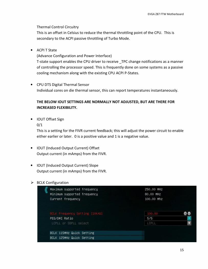
� BCLK Configuration
EVGA Z87 FTW Motherboard
16
• Maximum Supported Frequency
Maximum possible BCLK speed by direct BCLK adjustments and/or multiplier
adjustments
• Minimum Supported Frequency
Minimum available BCLK setting.
• Current Frequency
Displays the current BCLK speed.
• BCLK Frequency Setting [10khz]
Base clock frequency adjustment, this can be adjusted in 10 KHz increments by clicking
the +/- keys or by typing in the value directly.
Adjusting this value will yield very little performance difference, but may result in
connectivity loss from various installed peripherals or pre-attached components.
• PEG/DMI Ratio
Ratio adjustment between PCIE strap and IMC to allow for increased memory speeds.
• LCPLL or SBPLL Select
These are PLL blocks for BCLK/PCIe clock generation.
LCPLL - Has tighter tolerances and functions more efficiently, but has a more limited
BCLK margin.
SBPLL - Has more jitter due to looser tolerances, but will give you more potential
overhead for BCLK clocking.
� BCLK 115MHz Quick Setting
� BCLK 125MHz Quick Setting
115 and 125 are both base points for overclocks based off of a 1.25BLCK multiplier, 115
with a reduced BCLK value. The purpose of this setting is to achieve a higher memory
clock when pushing a high CPU clock frequency. This is a baseline adjustment; when
overclocking it is likely you will still need to adjust other values.
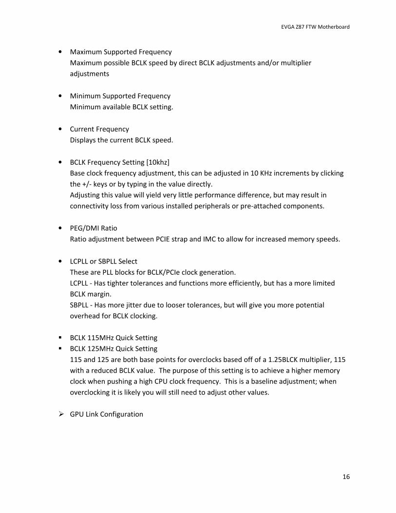
� GPU Link Configuration
EVGA Z87 FTW Motherboard
17
There are 4 GPU link settings, all options and ranges are identical, this is strictly for
adjusting up to 4 video cards individually.
• GPU 1 Vgpu Voltage
Voltage range is 1.000v – 2.000v
This is an adjustment for the GPU core voltage.
• GPU 1 Vmem Voltage
Voltage range is 1.000v – 2.500v
This is the adjustment for the RAM on the video card.
• GPU 1 Vaux Voltage
Voltage range is 0.700v – 1.500v
This is adjustment for PEX/PLL voltage on the video card.
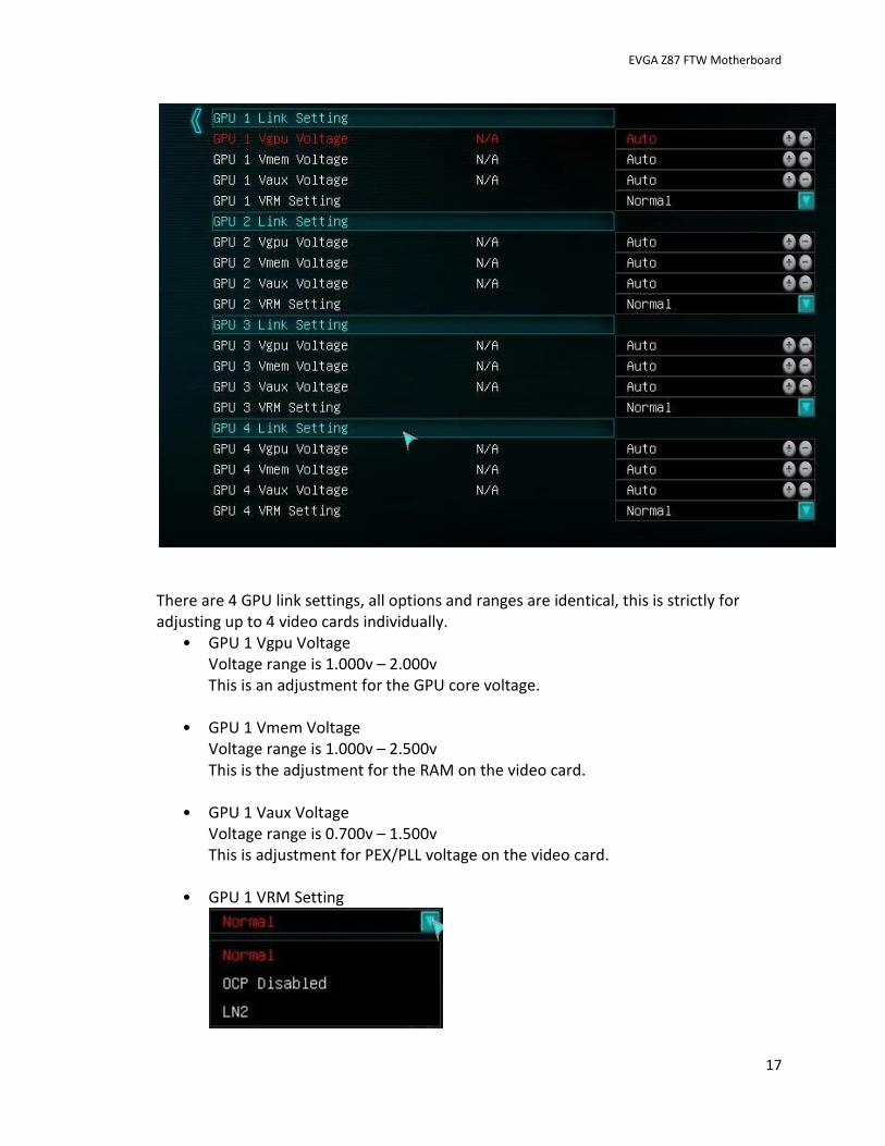
• GPU 1 VRM Setting
EVGA Z87 FTW Motherboard
18
• Normal – Leave all BIOS settings on the card at reference.
• OCP Disabled – This disables OCP to assist with the voltage increase that comes
with doing heavy overclocking on VGA.
• LN2 – This has several tweaks to the BIOS that are specific for running VGA at
sub-zero temperatures.
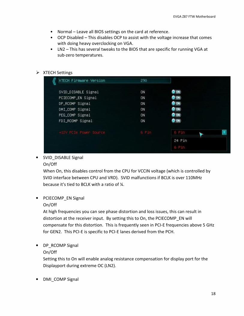
� XTECH Settings
• SVID_DISABLE Signal
On/Off
When On, this disables control from the CPU for VCCIN voltage (which is controlled by
SVID interface between CPU and VRD). SVID malfunctions if BCLK is over 110MHz
because it's tied to BCLK with a ratio of ¼.
• PCIECOMP_EN Signal
On/Off
At high frequencies you can see phase distortion and loss issues, this can result in
distortion at the receiver input. By setting this to On, the PCIECOMP_EN will
compensate for this distortion. This is frequently seen in PCI-E frequencies above 5 GHz
for GEN2. This PCI-E is specific to PCI-E lanes derived from the PCH.
• DP_RCOMP Signal
On/Off
Setting this to On will enable analog resistance compensation for display port for the
Displayport during extreme OC (LN2).
• DMI_COMP Signal
EVGA Z87 FTW Motherboard
19
On/Off
At high frequencies you can see phase distortion and loss issues, this can result in
distortion at the receiver input. By setting this to On, the DMI_COMP will compensate
for this distortion. This is frequently seen in PCI-E frequencies above 5 GHz for GEN2.
This PCI-E is specific to PCI-E lanes derived from the PCH.
• PEG_COMP Signal
On/Off
At high frequencies you can see phase distortion and loss issues, this can result in
distortion at the receiver input. By setting this to On, the PEG_COMP will compensate
for this distortion. This is frequently seen in PCI-E frequencies above 5 GHz for GEN2.
This PEG Compensation Signal is specific to PCI-E lanes derived from CPU.
• FDI_RCOMP Signal
Flexible Display Interface_ Reference and Compensation Signals
The buffer for the FDI in the Display Interface Signal. By setting this to On, the
RDI_RCOMP will compensate for the distortion in the Display Interface Signal.
On/Off
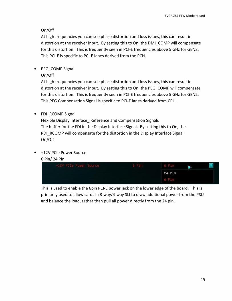
• +12V PCIe Power Source
6 Pin/ 24 Pin
This is used to enable the 6pin PCI-E power jack on the lower edge of the board. This is
primarily used to allow cards in 3-way/4-way SLI to draw additional power from the PSU
and balance the load, rather than pull all power directly from the 24 pin.
EVGA Z87 FTW Motherboard
20
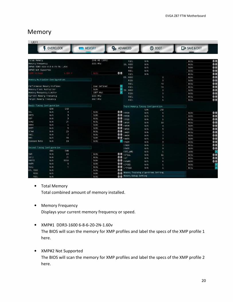
Memory
• Total Memory
Total combined amount of memory installed.
• Memory Frequency
Displays your current memory frequency or speed.
• XMP#1 DDR3-1600 6-8-6-20-2N-1.60v
The BIOS will scan the memory for XMP profiles and label the specs of the XMP profile 1
here.
• XMP#2 Not Supported
The BIOS will scan the memory for XMP profiles and label the specs of the XMP profile 2
here.
EVGA Z87 FTW Motherboard
21
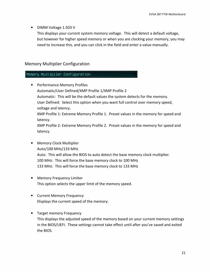
• DIMM Voltage 1.503 V
This displays your current system memory voltage. This will detect a default voltage,
but however for higher speed memory or when you are clocking your memory, you may
need to increase this, and you can click in the field and enter a value manually.
Memory Multiplier Configuration
• Performance Memory Profiles
Automatic/User Defined/XMP Profile 1/XMP Profile 2
Automatic: This will be the default values the system detects for the memory.
User Defined: Select this option when you want full control over memory speed,
voltage and latency.
XMP Profile 1: Extreme Memory Profile 1. Preset values in the memory for speed and
latency.
XMP Profile 2: Extreme Memory Profile 2. Preset values in the memory for speed and
latency.
• Memory Clock Multiplier
Auto/100 MHz/133 MHz
Auto: This will allow the BIOS to auto detect the base memory clock multiplier.
100 MHz: This will force the base memory clock to 100 MHz
133 MHz: This will force the base memory clock to 133 MHz
• Memory Frequency Limiter
This option selects the upper limit of the memory speed.
• Current Memory Frequency
Displays the current speed of the memory.
• Target memory Frequency
This displays the adjusted speed of the memory based on your current memory settings
in the BIOS/UEFI. These settings cannot take effect until after you’ve saved and exited
the BIOS.
EVGA Z87 FTW Motherboard
22
**Under normal circumstances Current and Target Memory Frequency will be the
same, however there will be differences like what is shown in the picture when you
are in process of changing memory speeds.**
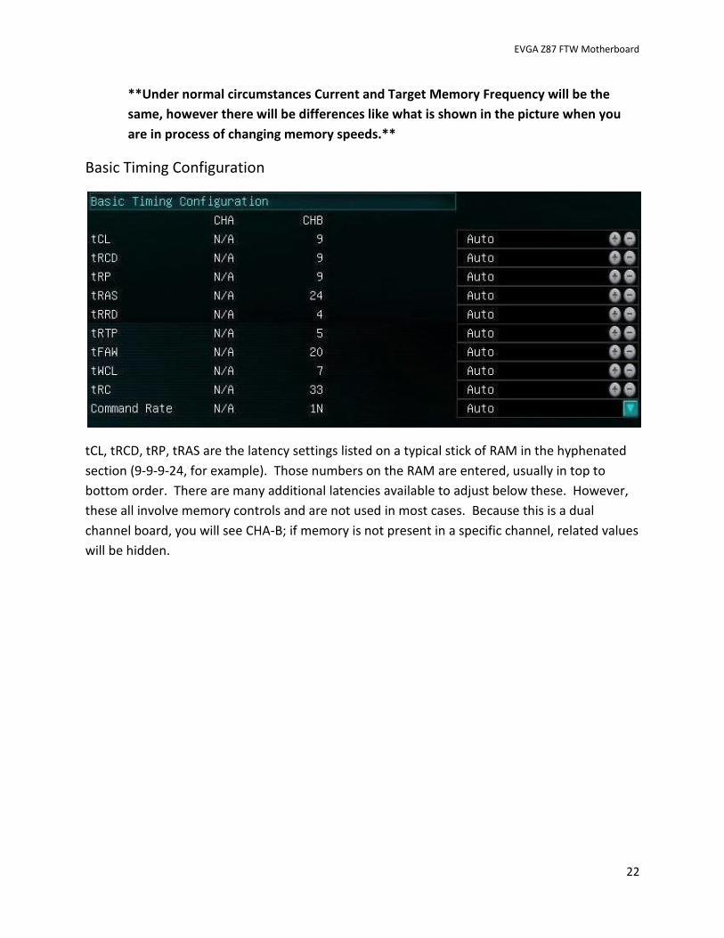
Basic Timing Configuration
tCL, tRCD, tRP, tRAS are the latency settings listed on a typical stick of RAM in the hyphenated
section (9-9-9-24, for example). Those numbers on the RAM are entered, usually in top to
bottom order. There are many additional latencies available to adjust below these. However,
these all involve memory controls and are not used in most cases. Because this is a dual
channel board, you will see CHA-B; if memory is not present in a specific channel, related values
will be hidden.
EVGA Z87 FTW Motherboard
23
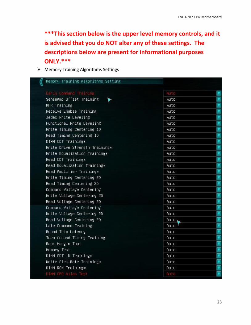
***This section below is the upper level memory controls, and it
is advised that you do NOT alter any of these settings. The
descriptions below are present for informational purposes
ONLY.***
� Memory Training Algorithms Settings
EVGA Z87 FTW Motherboard
24
• Early Command Training
Early Command Training is the initial step after reading SPD and configuring DDR
interface to desired speed/timings.
It delays and offsets to DDR clock to have all command lines in sync with a clock. Traces
inside CPU, on board, and inside DIMM have different lengths and data arrives at
different times, so this training tries to add compensation for those delays to have
everything clocked within valid time slots.
• SenseAmp Offset Training
Sense amplifier is to sense the low power signals from a bitline which represents a data
bit (1 or 0) stored in a memory cell, and amplify the small voltage swing to recognizable
logic levels so the data can be interpreted properly by logic outside the memory.
• MPR Training
Multi Purpose Register
During Read Leveling the memory controller adjusts for the delays introduced by the fly-
by memory topology that impacts the read cycle. The MPR can be loaded with
predefined data values via a special command from the memory controller. These data
values can be used for system timing calibration by the memory controller.
• Receive Enable Training
Receive enable is a step for adjustment I/O and prepare receivers to start operation on
desired speed/timings. After this step memory controller is ready to receive first raw
data on bus.
• Jedec Write Leveling
Write leveling was added to DDR3 to remove the skew between the
command/address/control/clocks busses and each of the DRAM data buses.
• Functional Write Leveling
Write leveling provides better signal integrity. The fly-by topology has the benefit of
reducing the number of stubs and their length, but it also causes flight time skew
between clock and strobe at every DRAM chip on the DIMM. Therefore, the DDR3
SDRAM supports a ‘write leveling’ feature to allow the controller to compensate for
skew.
• Write Timing Centering 1D
EVGA Z87 FTW Motherboard
25
This step adjusts delays for writes to DRAMs across DIMMs, tests and adjusts
termination settings. DDR3 is fly-by topology, with DRAM chips on a rope between
them, so with every next DRAM there will be more and more delay. So on this stage MC
tries to compensate timing/delays for write operations, across all bits. This setting only
affects write delays, hence one dimension (1D).
• Read Timing Centering 1D
Memory Controller will write test data into RAM, and receive it back to do similar step
and delay compensation, but this time on receiver side of MC. Counterpart to Write
Timing Centering, also does not interact voltage margin.
• DIMM ODT Training*
On-Die Termination
A semiconductor based termination scheme to reduce electrical 'noise' in the signal of
the memory bus, specifically reflections on the data bus of a memory subsystem and
eliminate bounce back of electrical signals on the high speed transmission lines for these
electrical traces/connections. Electrical signals can be reflected at points where
impedance differs, such as at the bus and at DRAM connection points. ODT resistors are
built into each DDR3 memory chip and eliminates the need for having terminating
resistors built into the motherboard. The ODT resistors in the chip are deactivated when
the chip is in use and reactivated when the chip is in standby mode.
• Write Drive Strength Leveling*
Drive strength leveling is a function for balancing timing for memory latency when
accounting for driver current as well as active resistance. This is for the timing between
the DQS (Data Queue Strobe) and the clock signals on each device.
• Write Equalization Training*
Equalization is a methodology to compensate for frequency dependent loss on the
connections between drivers and receivers.
• Read Amplifier Training*
Data received through the pins initially suffer from signal degradation, and need to be
recovered/equalized correctly. This is done through certain analog units from within the
IMC and the DRAM cells, specifically row and column amplifiers. The memory controller
adjusts amplifiers to get the best margin for voltage levels for all data bits.
• Write Timing Centering 2D

EVGA Z87 FTW Motherboard
26
There is a range of timing (horizontal margin) and delays in which DRAM will give valid
data. This function tests how many steps in each direction the DRAM can move before
the DRAM fails to successfully write. As this tests for both timing and delays it is
referred to as a 2D Write test.
• Read Timing Centering 2D
There is a range of timing (horizontal margin) and delays in which DRAM will give valid
data. This function tests how many steps in each direction the DRAM can move before
the DRAM fails to successfully write. As this tests for both timing and delays it is
referred to as a 2D Read test.
• Command Voltage Centering
This is a voltage margin test for the memory controller. Keeping a higher margin is very
helpful for heavy memory use as all command lines are shared on all DIMMs, this is also
very important on memory volumes above 8gb.
• Write Voltage Centering 2D
There is a range of voltage (vertical margin) and delays in which DRAM will give valid
data. This function tests how many steps in each direction the DRAM can move before
the DRAM fails to successfully write. As this tests for both timing and delays it is
referred to as a 2D Write Test.
• Read Voltage Centering 2D
There is a range of voltage (vertical margin) and delays in which DRAM will give valid
data. This function tests how many steps in each direction the DRAM can move before
the DRAM fails to successfully write. As this tests for both timing and delays it is
referred to as a 2D Read test.
• Late Command Training
Once data and command margins are set and ready, upper level delays are adjusted and
pattern tests are run.
• Round Trip Latency
DRAM RTL is measured in memory controller clock cycles rather than DRAM bus cycles.
The RTL parameters define the number of memory controller cycles that elapse before
data is returned to the memory controller after a read CAS command is issued. The RTL
setting works to fine tune DRAM buffer output latency. This setting is auto-sensed by

EVGA Z87 FTW Motherboard
27
the memory controller during the POST process, and usually not recommended to
adjust.
• Turn Around Timing Training
Turn around timing is the delay when a command/data is sent from the memory
controller to the DIMM and then returns to the Memory Controller. Adjustment for this
timing is handled internally and is necessary for proper operation within the OS.
• Rank Margin Tool
This is a debug tool, which shows test results and margins data regarding the various
settings listed above, and this is not for use of the end user, but at the engineering level.
• Memory Test
A simplified internal memory test.
• DIMM ODT 1D Training*
On-die termination single-dimension training, to adjust proper loading settings on
signals. If the signal is not properly terminated the signal will be reflected back and forth
causing severe signal degradation. Training helps to resolve this issue.
• Write Slew Rate Training*
One variable on DDR signals is a slope time and/or shape for fast transients.
Transceivers can drive signals fast and sharp, but that may cause excessive ringing,
reflections, in some instances it is preferred to have driving strength reduced and raise
signal at a slower rate. This training tries to improve margins by sweeping slew rate
speed.
• DIMM RON Training*
Resistance on DIMM's I/O is not a constant. This training feature helps to normalize it,
so the memory controller is prepared for signal variation.
• DIMM SPD Alias Test
Logic check for correct SPD data.
EVGA Z87 FTW Motherboard
28
� Memory Debug Setting
• Max TOLUD
Top of Low Used DRAM
TOLUD controls CPU memory range occupied by the DRAM below 4GB. Remap base is
only in use if the system DRAM size is equal to or larger than 4GB; in this case remap
base marks the end of the “normal” CPU DRAM range above 4GB.
• Enh (Enhanced) Interleave Support
Enable/Disable
Interleaving allows data to be written to multiple DIMMs simultaneously, rather than
sequentially.
• RI (Rank Interleave) Support
Enable/Disable
Interleaves physical ranks of memory so that a rank can be accessed while another is
being refreshed. Performance gains depend on the application in question.
• DLL Weak Lock Support
Part of the Memory Controller I/O, allows for locking the memory heap from being used
by runtime libraries. Contention of this lock can limit the performance benefits from
multithreaded applications.
EVGA Z87 FTW Motherboard
29
• Mc (Memory Controller) Lock
MC (Memory Controller) locks the 16 byte-aligned memory block that was addressed in
the address phase.
• Ch Hash Support
Checksums and data validity/integrity checks.
• Ch Hash Mask
Checksums and data validity/integrity checks.
• Ch Hash Interleaved Bit
Checksums and data validity/integrity checks.
• Memory Scrambler
DDR Data Scrambler to reduce power supply noise, improve signal integrity and to
encrypt/protect the contents of memory.
• MRC Fast Boot
Bypasses longer memory training routines during system re-BOOT. Can help speed up
BOOT times. If using higher memory frequency divider ratios (DDR3-2133 and over),
then disabling this setting while trying to achieve stability can be beneficial. Once the
desired system stability has obtained, Enable this setting to prevent the auto sensed
parameters from drifting on subsequent system re-BOOTs.
• DIMM Exit Mode
Select Slow Exit to reduce power consumption, or Fast Exit for better performance.
• Memory Remap
Check the BIOS settings to see whether the memory remapping feature is enabled.
Memory remapping gives Windows access to more memory. You can enable the
memory remapping feature in the BIOS by booting to the system setup.
This is largely only needed by 32 bit versions of MODERN operating systems, such as
Windows 7.
• Channel A DIMM Control
This allows a user to disable a channel without physically removing the DIMM. Leave on
Auto unless experimenting or testing individual channels for stability.

EVGA Z87 FTW Motherboard
30
• Channel B DIMM Control
This allows a user to disable a channel without physically removing the DIMM. Leave on
Auto unless experimenting or testing individual channels for stability.
EVGA Z87 FTW Motherboard
31
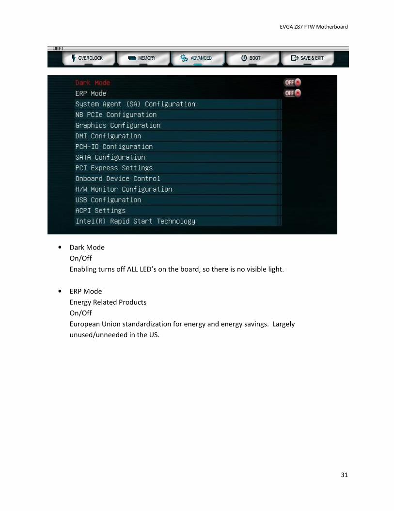
• Dark Mode
On/Off
Enabling turns off ALL LED’s on the board, so there is no visible light.
• ERP Mode
Energy Related Products
On/Off
European Union standardization for energy and energy savings. Largely
unused/unneeded in the US.
EVGA Z87 FTW Motherboard
32
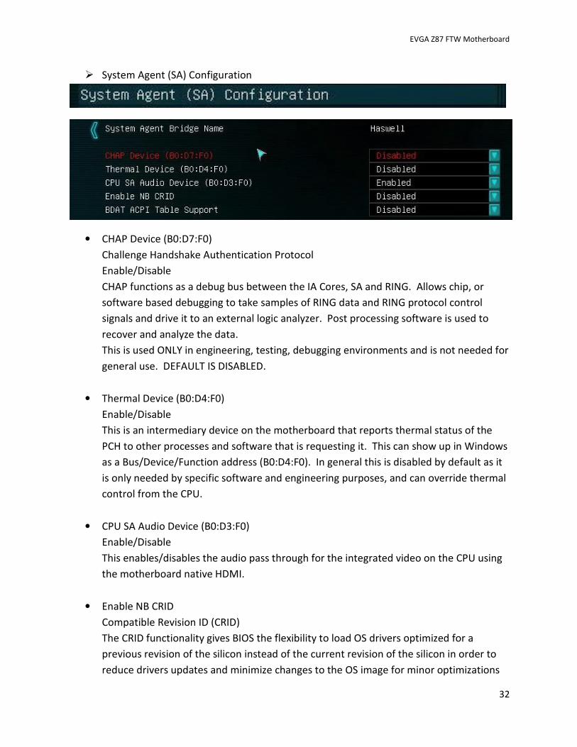
� System Agent (SA) Configuration
• CHAP Device (B0:D7:F0)
Challenge Handshake Authentication Protocol
Enable/Disable
CHAP functions as a debug bus between the IA Cores, SA and RING. Allows chip, or
software based debugging to take samples of RING data and RING protocol control
signals and drive it to an external logic analyzer. Post processing software is used to
recover and analyze the data.
This is used ONLY in engineering, testing, debugging environments and is not needed for
general use. DEFAULT IS DISABLED.
• Thermal Device (B0:D4:F0)
Enable/Disable
This is an intermediary device on the motherboard that reports thermal status of the
PCH to other processes and software that is requesting it. This can show up in Windows
as a Bus/Device/Function address (B0:D4:F0). In general this is disabled by default as it
is only needed by specific software and engineering purposes, and can override thermal
control from the CPU.
• CPU SA Audio Device (B0:D3:F0)
Enable/Disable
This enables/disables the audio pass through for the integrated video on the CPU using
the motherboard native HDMI.
• Enable NB CRID
Compatible Revision ID (CRID)
The CRID functionality gives BIOS the flexibility to load OS drivers optimized for a
previous revision of the silicon instead of the current revision of the silicon in order to
reduce drivers updates and minimize changes to the OS image for minor optimizations
EVGA Z87 FTW Motherboard
33
to the silicon for yield improvement, or feature enhancement reasons that do not
negatively impact the OS driver functionality.
Enable/Disable
• BDAT ACPI Table Support
Enable/Disable
This is an ACPI table that is stored in memory. Typically only used on a system hosting
virtual machines, and even then it is not necessary, unless the application specifically
requires it. Default is DISABLED.
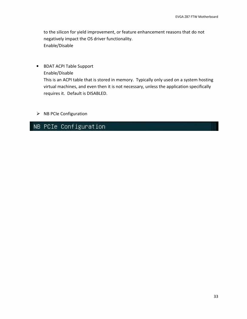
� NB PCIe Configuration

EVGA Z87 FTW Motherboard
34
• PEG0 – Gen X
• PEG1 – Gen X
• PEG2 – Gen X
EVGA Z87 FTW Motherboard
35
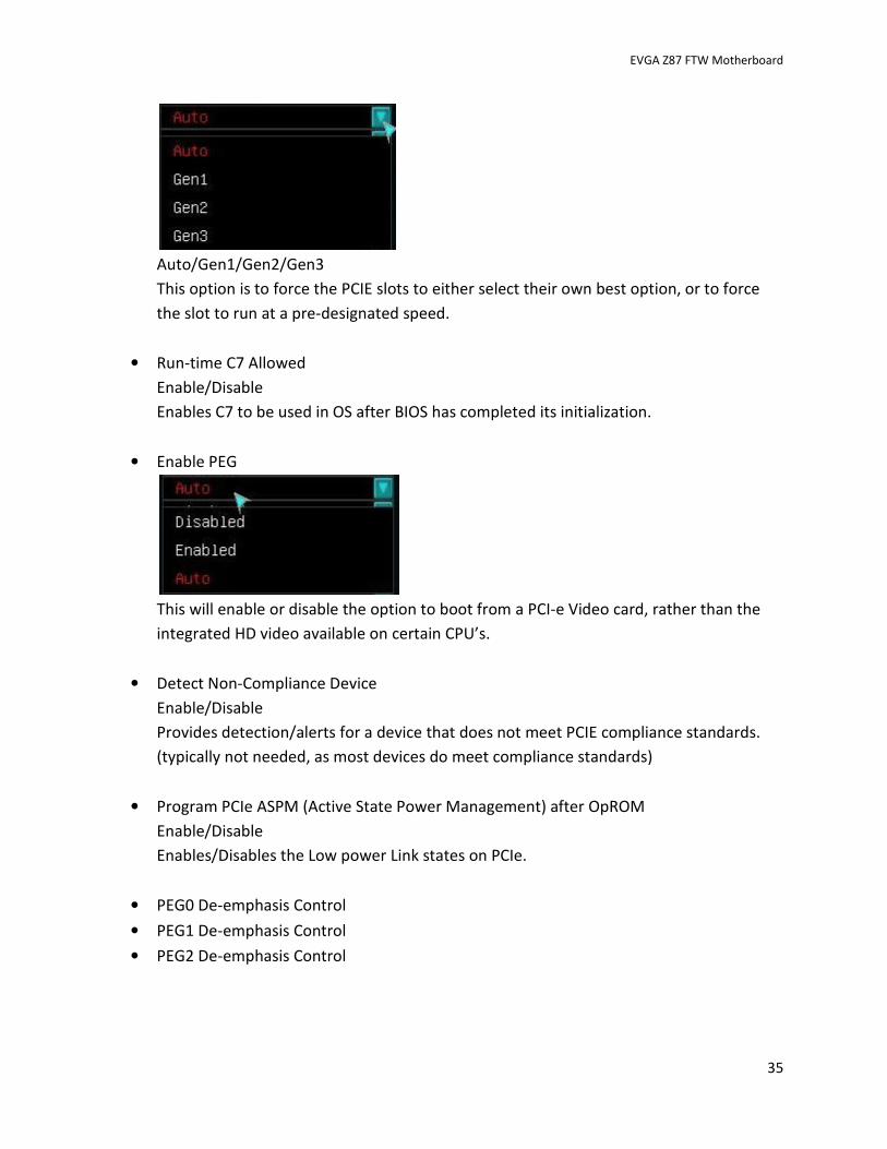
Auto/Gen1/Gen2/Gen3
This option is to force the PCIE slots to either select their own best option, or to force
the slot to run at a pre-designated speed.
• Run-time C7 Allowed
Enable/Disable
Enables C7 to be used in OS after BIOS has completed its initialization.
• Enable PEG
This will enable or disable the option to boot from a PCI-e Video card, rather than the
integrated HD video available on certain CPU’s.
• Detect Non-Compliance Device
Enable/Disable
Provides detection/alerts for a device that does not meet PCIE compliance standards.
(typically not needed, as most devices do meet compliance standards)
• Program PCIe ASPM (Active State Power Management) after OpROM
Enable/Disable
Enables/Disables the Low power Link states on PCIe.
• PEG0 De-emphasis Control
• PEG1 De-emphasis Control
• PEG2 De-emphasis Control
EVGA Z87 FTW Motherboard
36
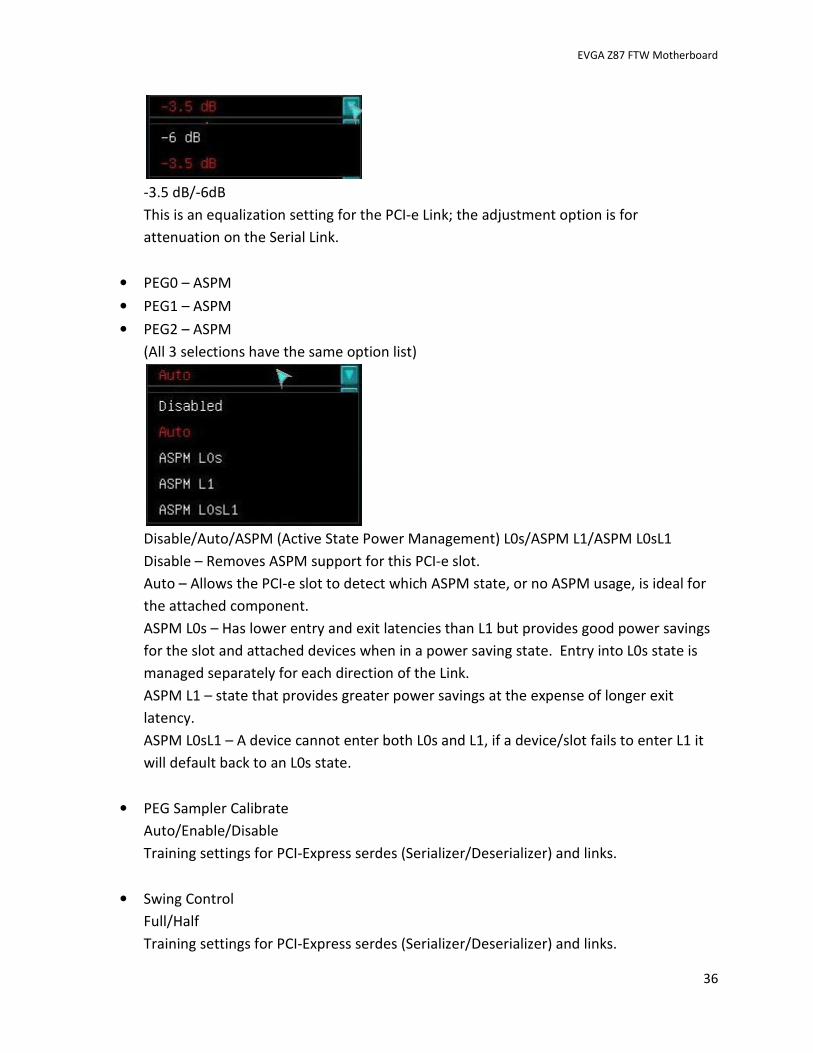
-3.5 dB/-6dB
This is an equalization setting for the PCI-e Link; the adjustment option is for
attenuation on the Serial Link.
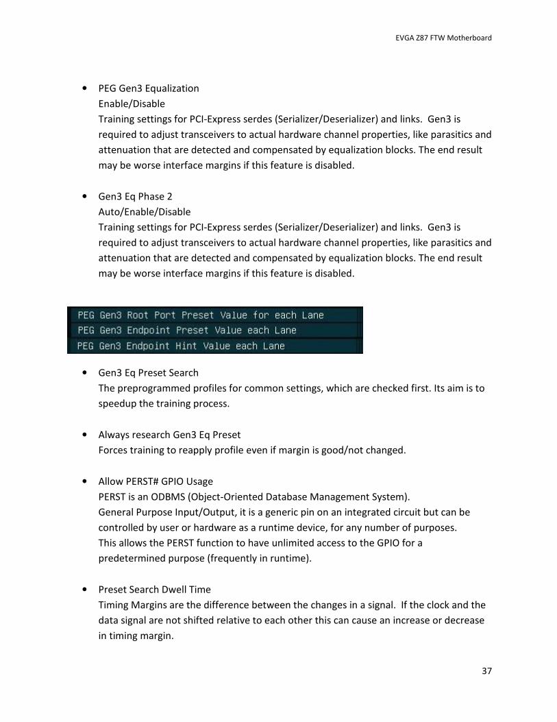
• PEG0 – ASPM
• PEG1 – ASPM
• PEG2 – ASPM
(All 3 selections have the same option list)
Disable/Auto/ASPM (Active State Power Management) L0s/ASPM L1/ASPM L0sL1
Disable – Removes ASPM support for this PCI-e slot.
Auto – Allows the PCI-e slot to detect which ASPM state, or no ASPM usage, is ideal for
the attached component.
ASPM L0s – Has lower entry and exit latencies than L1 but provides good power savings
for the slot and attached devices when in a power saving state. Entry into L0s state is
managed separately for each direction of the Link.
ASPM L1 – state that provides greater power savings at the expense of longer exit
latency.
ASPM L0sL1 – A device cannot enter both L0s and L1, if a device/slot fails to enter L1 it
will default back to an L0s state.
• PEG Sampler Calibrate
Auto/Enable/Disable
Training settings for PCI-Express serdes (Serializer/Deserializer) and links.
• Swing Control
Full/Half
Training settings for PCI-Express serdes (Serializer/Deserializer) and links.
EVGA Z87 FTW Motherboard
37
• PEG Gen3 Equalization
Enable/Disable
Training settings for PCI-Express serdes (Serializer/Deserializer) and links. Gen3 is
required to adjust transceivers to actual hardware channel properties, like parasitics and
attenuation that are detected and compensated by equalization blocks. The end result
may be worse interface margins if this feature is disabled.
• Gen3 Eq Phase 2
Auto/Enable/Disable
Training settings for PCI-Express serdes (Serializer/Deserializer) and links. Gen3 is
required to adjust transceivers to actual hardware channel properties, like parasitics and
attenuation that are detected and compensated by equalization blocks. The end result
may be worse interface margins if this feature is disabled.
• Gen3 Eq Preset Search
The preprogrammed profiles for common settings, which are checked first. Its aim is to
speedup the training process.
• Always research Gen3 Eq Preset
Forces training to reapply profile even if margin is good/not changed.
• Allow PERST# GPIO Usage
PERST is an ODBMS (Object-Oriented Database Management System).
General Purpose Input/Output, it is a generic pin on an integrated circuit but can be
controlled by user or hardware as a runtime device, for any number of purposes.
This allows the PERST function to have unlimited access to the GPIO for a
predetermined purpose (frequently in runtime).
• Preset Search Dwell Time
Timing Margins are the difference between the changes in a signal. If the clock and the
data signal are not shifted relative to each other this can cause an increase or decrease
in timing margin.

EVGA Z87 FTW Motherboard
38
• Timing Margin Steps
Allows for incremental Margin Changes in signal timing.
• Timing Start Margin
Gives a predefined start value for Timing Margins.
• Voltage Margin Steps
This sets the coarseness of the vertical detection algorithm by adjusting the voltage step
size.
• Voltage Start margin
Gives a predefined start value for Voltage Margins.
• Favor Timing Margin
Gives priority to timing adjustment, rather than have voltage+timing treatment equal.
• Error Target
With the equalization steps, the error target is set to a default value of 1. If the
equalization attempt fails, it will not retry the correction. Raising the value allows for
the equalization to retry as many times as needed until it reaches the set limit.
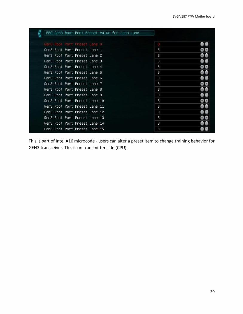
� PEG Gen3 Root Port Preset Value for each Lane
EVGA Z87 FTW Motherboard
39
This is part of Intel A16 microcode - users can alter a preset item to change training behavior for
GEN3 transceiver. This is on transmitter side (CPU).
EVGA Z87 FTW Motherboard
40
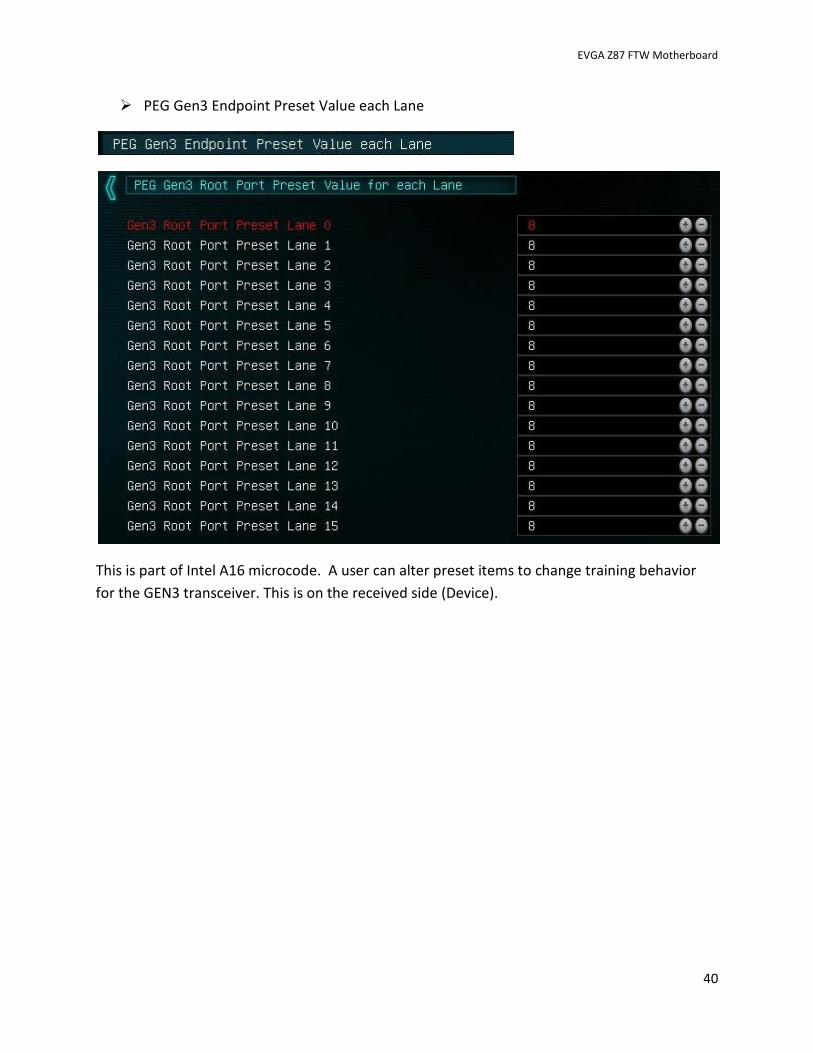
� PEG Gen3 Endpoint Preset Value each Lane
This is part of Intel A16 microcode. A user can alter preset items to change training behavior
for the GEN3 transceiver. This is on the received side (Device).
EVGA Z87 FTW Motherboard
41
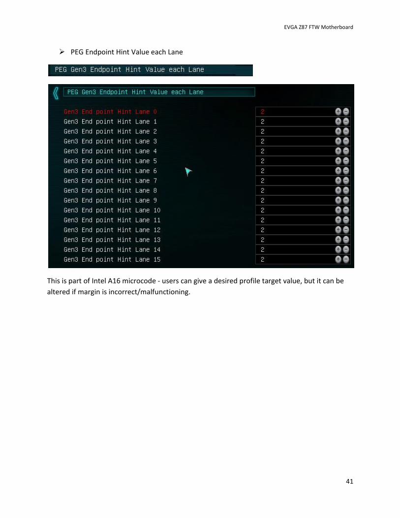
� PEG Endpoint Hint Value each Lane
This is part of Intel A16 microcode - users can give a desired profile target value, but it can be
altered if margin is incorrect/malfunctioning.
EVGA Z87 FTW Motherboard
42
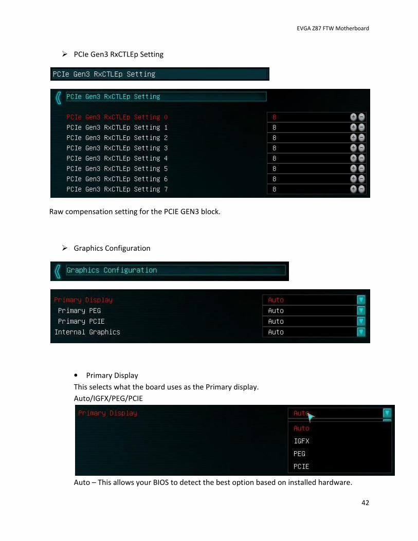
� PCIe Gen3 RxCTLEp Setting
Raw compensation setting for the PCIE GEN3 block.
� Graphics Configuration
• Primary Display
This selects what the board uses as the Primary display.
Auto/IGFX/PEG/PCIE
Auto – This allows your BIOS to detect the best option based on installed hardware.
EVGA Z87 FTW Motherboard
43
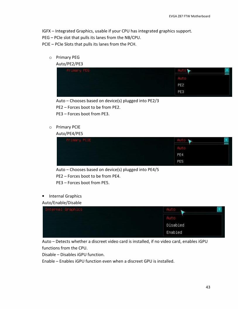
IGFX – Integrated Graphics, usable if your CPU has integrated graphics support.
PEG – PCIe slot that pulls its lanes from the NB/CPU.
PCIE – PCIe Slots that pulls its lanes from the PCH.
o Primary PEG
Auto/PE2/PE3
Auto – Chooses based on device(s) plugged into PE2/3
PE2 – Forces boot to be from PE2.
PE3 – Forces boot from PE3.
o Primary PCIE
Auto/PE4/PE5
Auto – Chooses based on device(s) plugged into PE4/5
PE2 – Forces boot to be from PE4.
PE3 – Forces boot from PE5.
• Internal Graphics
Auto/Enable/Disable
Auto – Detects whether a discreet video card is installed, if no video card, enables iGPU
functions from the CPU.
Disable – Disables iGPU function.
Enable – Enables iGPU function even when a discreet GPU is installed.
EVGA Z87 FTW Motherboard
44
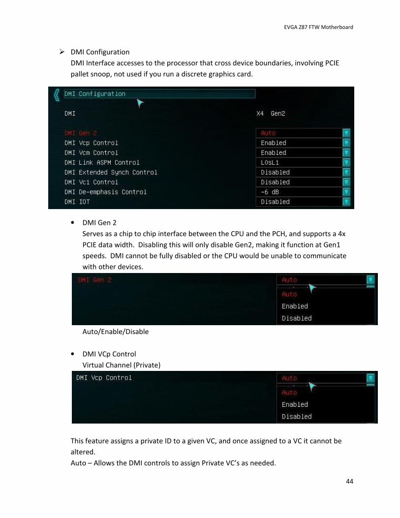
� DMI Configuration
DMI Interface accesses to the processor that cross device boundaries, involving PCIE
pallet snoop, not used if you run a discrete graphics card.
• DMI Gen 2
Serves as a chip to chip interface between the CPU and the PCH, and supports a 4x
PCIE data width. Disabling this will only disable Gen2, making it function at Gen1
speeds. DMI cannot be fully disabled or the CPU would be unable to communicate
with other devices.
Auto/Enable/Disable
• DMI VCp Control
Virtual Channel (Private)
This feature assigns a private ID to a given VC, and once assigned to a VC it cannot be
altered.
Auto – Allows the DMI controls to assign Private VC’s as needed.
EVGA Z87 FTW Motherboard
45
Enable – Enables the use of Private VC upon device request.
Disable – Removes the option for VCp.
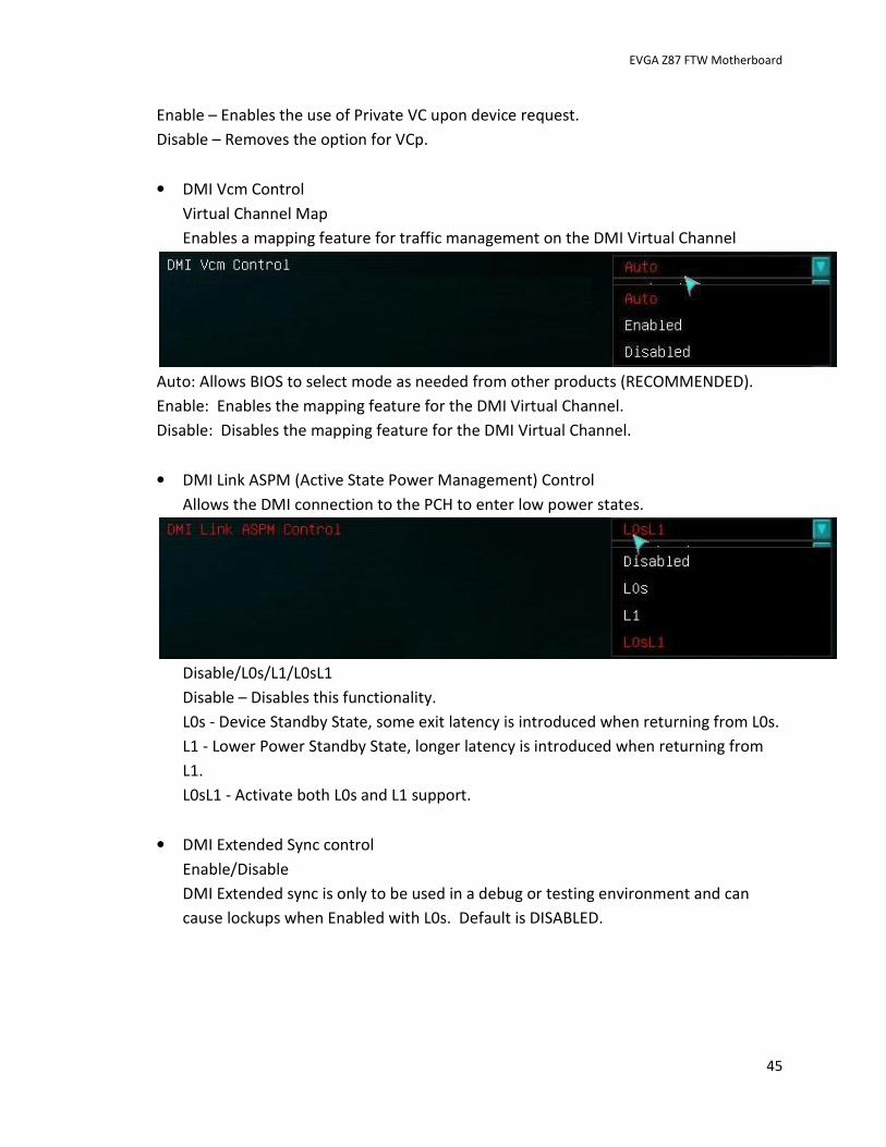
• DMI Vcm Control
Virtual Channel Map
Enables a mapping feature for traffic management on the DMI Virtual Channel
Auto: Allows BIOS to select mode as needed from other products (RECOMMENDED).
Enable: Enables the mapping feature for the DMI Virtual Channel.
Disable: Disables the mapping feature for the DMI Virtual Channel.
• DMI Link ASPM (Active State Power Management) Control
Allows the DMI connection to the PCH to enter low power states.
Disable/L0s/L1/L0sL1
Disable – Disables this functionality.
L0s - Device Standby State, some exit latency is introduced when returning from L0s.
L1 - Lower Power Standby State, longer latency is introduced when returning from
L1.
L0sL1 - Activate both L0s and L1 support.
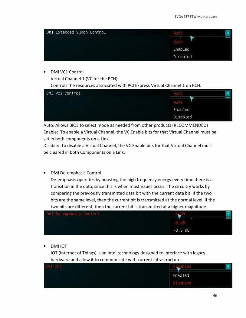
• DMI Extended Sync control
Enable/Disable
DMI Extended sync is only to be used in a debug or testing environment and can
cause lockups when Enabled with L0s. Default is DISABLED.
EVGA Z87 FTW Motherboard
46
• DMI VC1 Control
Virtual Channel 1 (VC for the PCH)
Controls the resources associated with PCI Express Virtual Channel 1 on PCH.
Auto: Allows BIOS to select mode as needed from other products (RECOMMENDED)
Enable: To enable a Virtual Channel, the VC Enable bits for that Virtual Channel must be
set in both components on a Link.
Disable: To disable a Virtual Channel, the VC Enable bits for that Virtual Channel must
be cleared in both Components on a Link.
• DMI De-emphasis Control
De-emphasis operates by boosting the high frequency energy every time there is a
transition in the data, since this is when most issues occur. The circuitry works by
comparing the previously transmitted data bit with the current data bit. If the two
bits are the same level, then the current bit is transmitted at the normal level. If the
two bits are different, then the current bit is transmitted at a higher magnitude.
• DMI IOT
IOT (Internet of Things) is an Intel technology designed to interface with legacy
hardware and allow it to communicate with current infrastructure.
EVGA Z87 FTW Motherboard
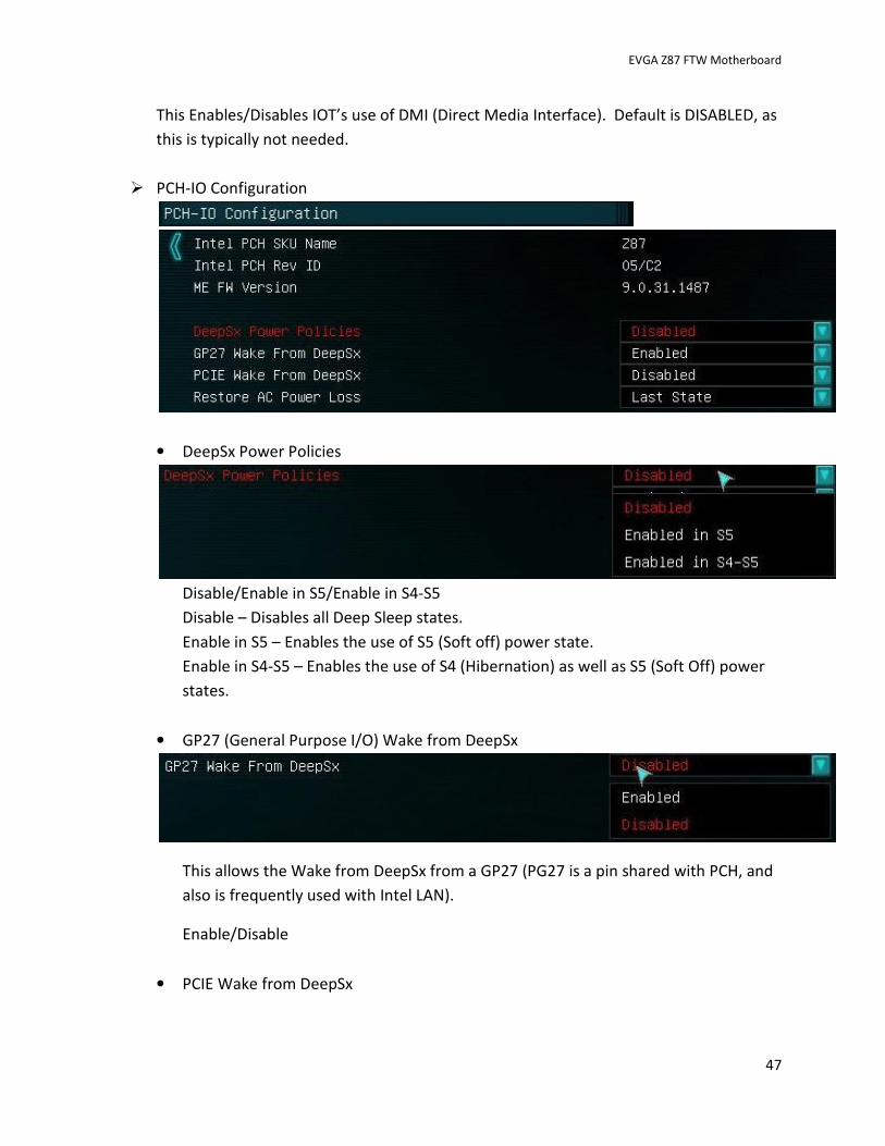
47
This Enables/Disables IOT’s use of DMI (Direct Media Interface). Default is DISABLED, as
this is typically not needed.
� PCH-IO Configuration
• DeepSx Power Policies
Disable/Enable in S5/Enable in S4-S5
Disable – Disables all Deep Sleep states.
Enable in S5 – Enables the use of S5 (Soft off) power state.
Enable in S4-S5 – Enables the use of S4 (Hibernation) as well as S5 (Soft Off) power
states.
• GP27 (General Purpose I/O) Wake from DeepSx
This allows the Wake from DeepSx from a GP27 (PG27 is a pin shared with PCH, and
also is frequently used with Intel LAN).
Enable/Disable
• PCIE Wake from DeepSx
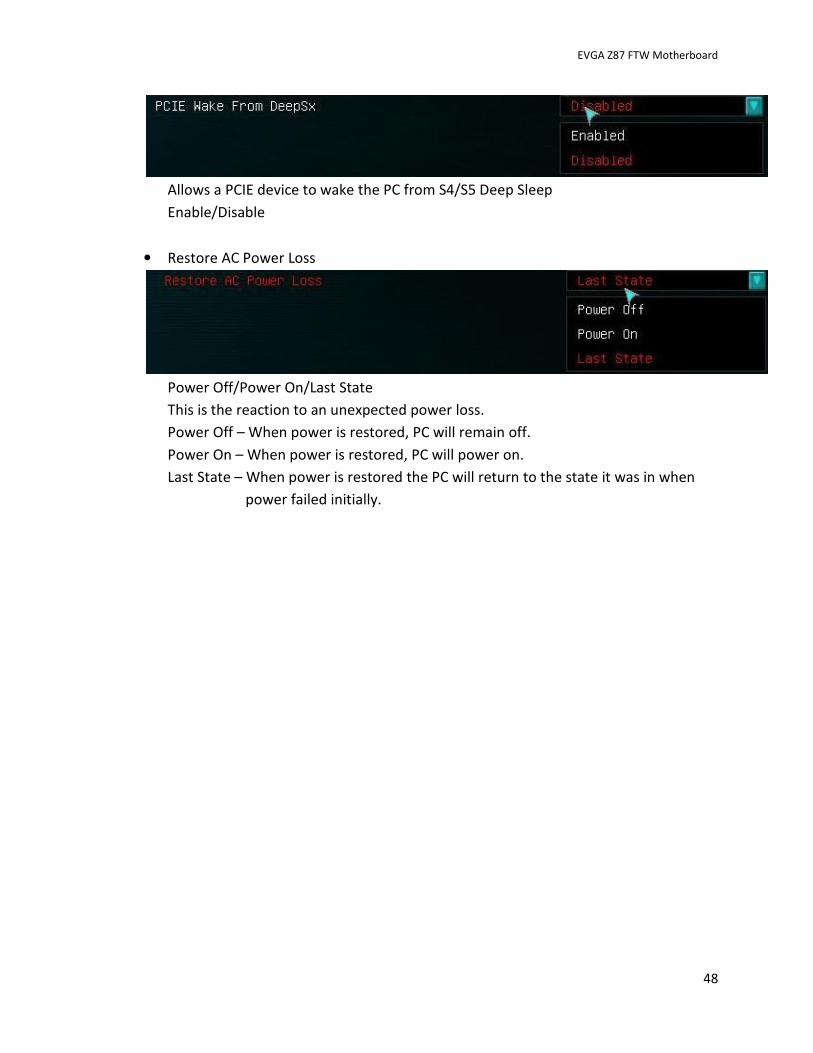
EVGA Z87 FTW Motherboard
48
Allows a PCIE device to wake the PC from S4/S5 Deep Sleep
Enable/Disable
• Restore AC Power Loss
Power Off/Power On/Last State
This is the reaction to an unexpected power loss.
Power Off – When power is restored, PC will remain off.
Power On – When power is restored, PC will power on.
Last State – When power is restored the PC will return to the state it was in when
power failed initially.
EVGA Z87 FTW Motherboard
49
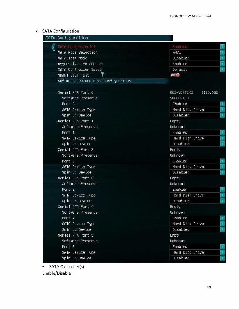
� SATA Configuration
• SATA Controller(s)
Enable/Disable
EVGA Z87 FTW Motherboard
50
Allows enabling and disabling the onboard SATA controller.
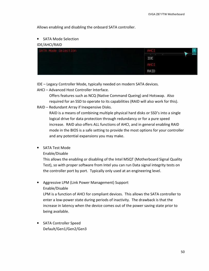
• SATA Mode Selection
IDE/AHCI/RAID
IDE – Legacy Controller Mode, typically needed on modern SATA devices.
AHCI – Advanced Host Controller Interface.
Offers features such as NCQ (Native Command Queing) and Hotswap. Also
required for an SSD to operate to its capabilities (RAID will also work for this).
RAID – Redundant Array if Inexpensive Disks.
RAID is a means of combining multiple physical hard disks or SSD’s into a single
logical drive for data protection through redundancy or for a pure speed
increase. RAID also offers ALL functions of AHCI, and in general enabling RAID
mode in the BIOS is a safe setting to provide the most options for your controller
and any potential expansions you may make.
• SATA Test Mode
Enable/Disable
This allows the enabling or disabling of the Intel MSQT (Motherboard Signal Quality
Test), so with proper software from Intel you can run Data signal integrity tests on
the controller port by port. Typically only used at an engineering level.
• Aggressive LPM (Link Power Management) Support
Enable/Disable
LPM is a function of AHCI for compliant devices. This allows the SATA controller to
enter a low-power state during periods of inactivity. The drawback is that the
increase in latency when the device comes out of the power saving state prior to
being available.
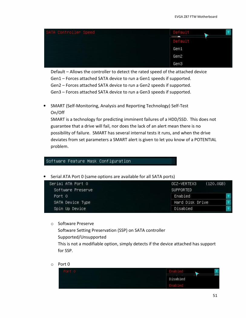
• SATA Controller Speed
Default/Gen1/Gen2/Gen3
EVGA Z87 FTW Motherboard
51
Default – Allows the controller to detect the rated speed of the attached device
Gen1 – Forces attached SATA device to run a Gen1 speeds if supported.
Gen2 – Forces attached SATA device to run a Gen2 speeds if supported.
Gen3 – Forces attached SATA device to run a Gen3 speeds if supported.
• SMART (Self-Monitoring, Analysis and Reporting Technology) Self-Test
On/Off
SMART is a technology for predicting imminent failures of a HDD/SSD. This does not
guarantee that a drive will fail, nor does the lack of an alert mean there is no
possibility of failure. SMART has several internal tests it runs, and when the drive
deviates from set parameters a SMART alert is given to let you know of a POTENTIAL
problem.
• Serial ATA Port 0 (same options are available for all SATA ports)
o Software Preserve
Software Setting Preservation (SSP) on SATA controller
Supported/Unsupported
This is not a modifiable option, simply detects if the device attached has support
for SSP.
o Port 0
EVGA Z87 FTW Motherboard
52
Enable/Disable
Enables/Disables the individual SATA port.
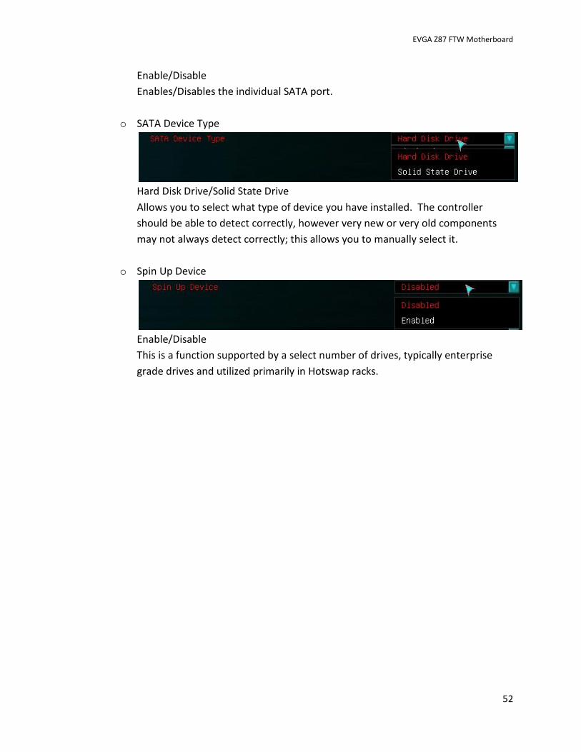
o SATA Device Type
Hard Disk Drive/Solid State Drive
Allows you to select what type of device you have installed. The controller
should be able to detect correctly, however very new or very old components
may not always detect correctly; this allows you to manually select it.
o Spin Up Device
Enable/Disable
This is a function supported by a select number of drives, typically enterprise
grade drives and utilized primarily in Hotswap racks.
EVGA Z87 FTW Motherboard
53
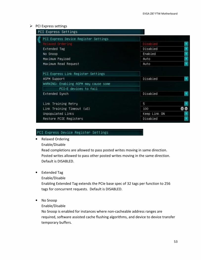
� PCI Express settings
• Relaxed Ordering
Enable/Disable
Read completions are allowed to pass posted writes moving in same direction.
Posted writes allowed to pass other posted writes moving in the same direction.
Default is DISABLED.
• Extended Tag
Enable/Disable
Enabling Extended Tag extends the PCIe base spec of 32 tags per function to 256
tags for concurrent requests. Default is DISABLED.
• No Snoop
Enable/Disable
No Snoop is enabled for instances where non-cacheable address ranges are
required, software assisted cache flushing algorithms, and device to device transfer
temporary buffers.
EVGA Z87 FTW Motherboard
54
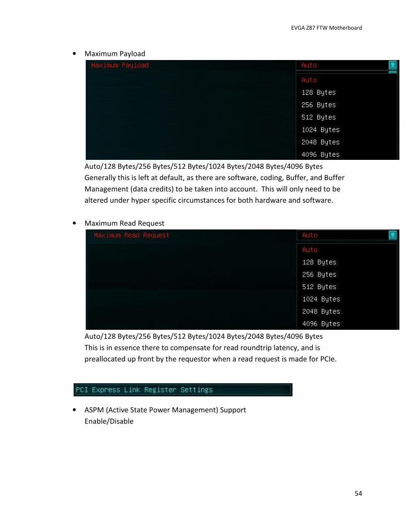
• Maximum Payload
Auto/128 Bytes/256 Bytes/512 Bytes/1024 Bytes/2048 Bytes/4096 Bytes
Generally this is left at default, as there are software, coding, Buffer, and Buffer
Management (data credits) to be taken into account. This will only need to be
altered under hyper specific circumstances for both hardware and software.
• Maximum Read Request
Auto/128 Bytes/256 Bytes/512 Bytes/1024 Bytes/2048 Bytes/4096 Bytes
This is in essence there to compensate for read roundtrip latency, and is
preallocated up front by the requestor when a read request is made for PCIe.
• ASPM (Active State Power Management) Support
Enable/Disable
EVGA Z87 FTW Motherboard
55
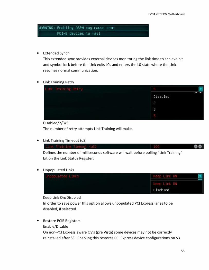
• Extended Synch
This extended sync provides external devices monitoring the link time to achieve bit
and symbol lock before the Link exits L0s and enters the L0 state where the Link
resumes normal communication.
• Link Training Retry
Disabled/2/3/5
The number of retry attempts Link Training will make.
• Link Training Timeout (uS)
Defines the number of milliseconds software will wait before polling “Link Training”
bit on the Link Status Register.
• Unpopulated Links
Keep Link On/Disabled
In order to save power this option allows unpopulated PCI Express lanes to be
disabled, if selected.
• Restore PCIE Registers
Enable/Disable
On non-PCI Express aware OS’s (pre Vista) some devices may not be correctly
reinstalled after S3. Enabling this restores PCI Express device configurations on S3
EVGA Z87 FTW Motherboard
56
resume. WARNING: This option may cause hardware issues with other hardware
after S3 resume.
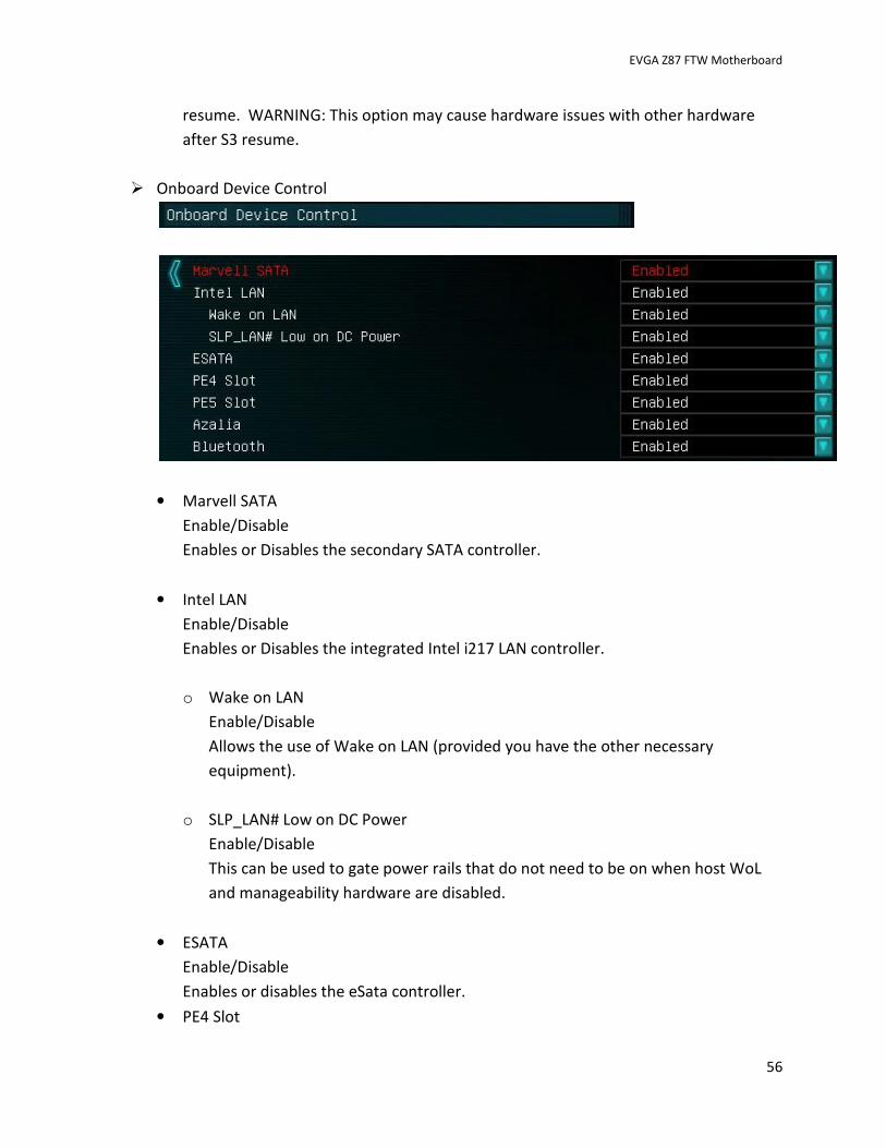
� Onboard Device Control
• Marvell SATA
Enable/Disable
Enables or Disables the secondary SATA controller.
• Intel LAN
Enable/Disable
Enables or Disables the integrated Intel i217 LAN controller.
o Wake on LAN
Enable/Disable
Allows the use of Wake on LAN (provided you have the other necessary
equipment).
o SLP_LAN# Low on DC Power
Enable/Disable
This can be used to gate power rails that do not need to be on when host WoL
and manageability hardware are disabled.
• ESATA
Enable/Disable
Enables or disables the eSata controller.
• PE4 Slot

EVGA Z87 FTW Motherboard
57
Enable/Disable
Enables or Disables the P4 (PCI-e 1x) Slot.
• PE5 Slot
Enable/Disable
Enables or Disables the P5 (Bottom PCI-e 16x) Slot.
• Azalia
Enable/Disable
Enables or disables the onboard Audio.
• Bluetooth
Enable/Disable
Enables or disables the integrated Bluetooth controller.
EVGA Z87 FTW Motherboard
58
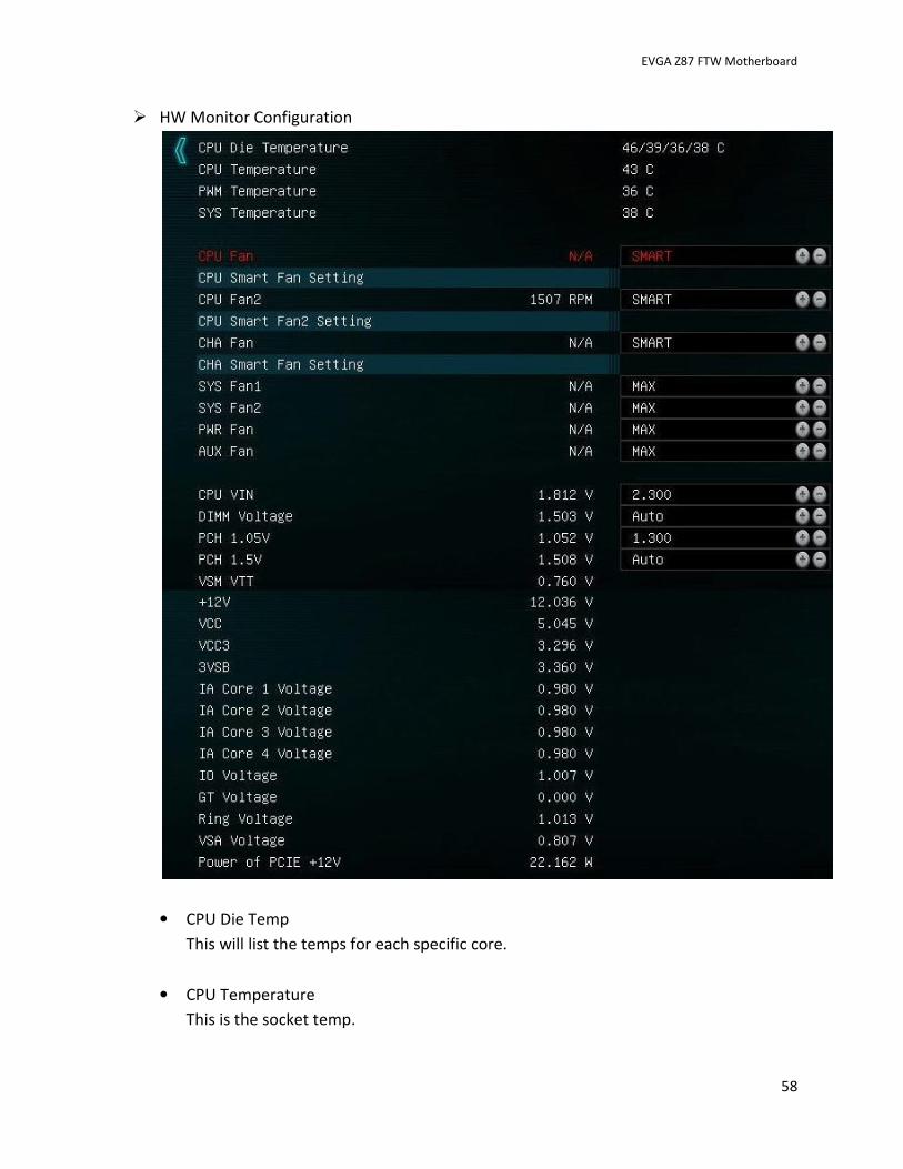
� HW Monitor Configuration
• CPU Die Temp
This will list the temps for each specific core.
• CPU Temperature
This is the socket temp.

EVGA Z87 FTW Motherboard
59
• PWM Temperature
This is the temperature of the PWM MOSFET’s.
• SYS Temperature
This is ambient case temp derived from an onboard thermal sensor.
• CPU Fan
SMART/manually entered value
Primary CPU fan header (PWM)
Can be left on SMART and the BIOS will adjust fan speed as necessary, or you can
use the +/- keys to adjust manually.
• CPU Fan2
SMART/manually entered value
Primary CPU fan header (PWM)
Can be left on SMART and the BIOS will adjust fan speed as necessary, or you can
use the +/- keys to adjust manually.
• CHA Fan
SMART/manually entered value
System fan header (PWM)
Can be left on SMART and the BIOS will adjust fan speed as necessary, or you can
use the +/- keys to adjust manually.
• SYS Fan1
MAX/manually entered value
System fan header (Voltage adjustment)
Can be left on SMART and the BIOS will adjust fan speed as necessary, or you can
use the +/- keys to adjust manually.
• SYS Fan2
MAX/manually entered value
System fan header (Voltage adjustment)
Can be left on SMART and the BIOS will adjust fan speed as necessary, or you can
use the +/- keys to adjust manually.
EVGA Z87 FTW Motherboard
60
• PWR Fan
MAX/manually entered value
System fan header (Voltage adjustment)
Can be left on SMART and the BIOS will adjust fan speed as necessary, or you can
use the +/- keys to adjust manually.
• AUX Fan
MAX/manually entered value
System fan header (Voltage adjustment)
Can be left on SMART and the BIOS will adjust fan speed as necessary, or you can
use the +/- keys to adjust manually.
• CPU VIN
• This is the only CPU VRM located on the motherboard’s PCB not controlled by the
FIVR. This voltage must be at least 0.4-0.6V higher than the set FIVR voltage. For
example, if the CPU Core voltage is set to 1.5V for extreme OC, VIN voltage must be
set to at least 2.1V. Higher voltage will cause higher temperatures for the CPU, the
increase in CPU VIN will reduce the efficiency of the voltage regulation.
Voltage range is 1.500V to 3.050V
• DIMM Voltage
This displays your current system memory voltage. This will detect a default voltage,
but for higher speed memory or when you are clocking your memory, you may need
to increase this, and you can click in the field and enter a value manually.
Voltage Range is 0.800V to 2.300V
Standard operating voltage range is 1.200V to 1.650V
• PCH 1.05V
Platform Controller Hub
PCH serves as a south bridge for modern Intel Chipsets
1.1v is the base voltage core for the PCH Core Domain
Voltage range is 0.700V to 1.600V
EVGA Z87 FTW Motherboard
61
• PCH 1.5V
Platform Controller Hub
PCH serves as a south bridge for modern Intel Chipsets
1.5v adjustments control the voltage for the PCH I/O and the IVR (Input Voltage
Range)
Voltage Range is 1.200V to 2.000V
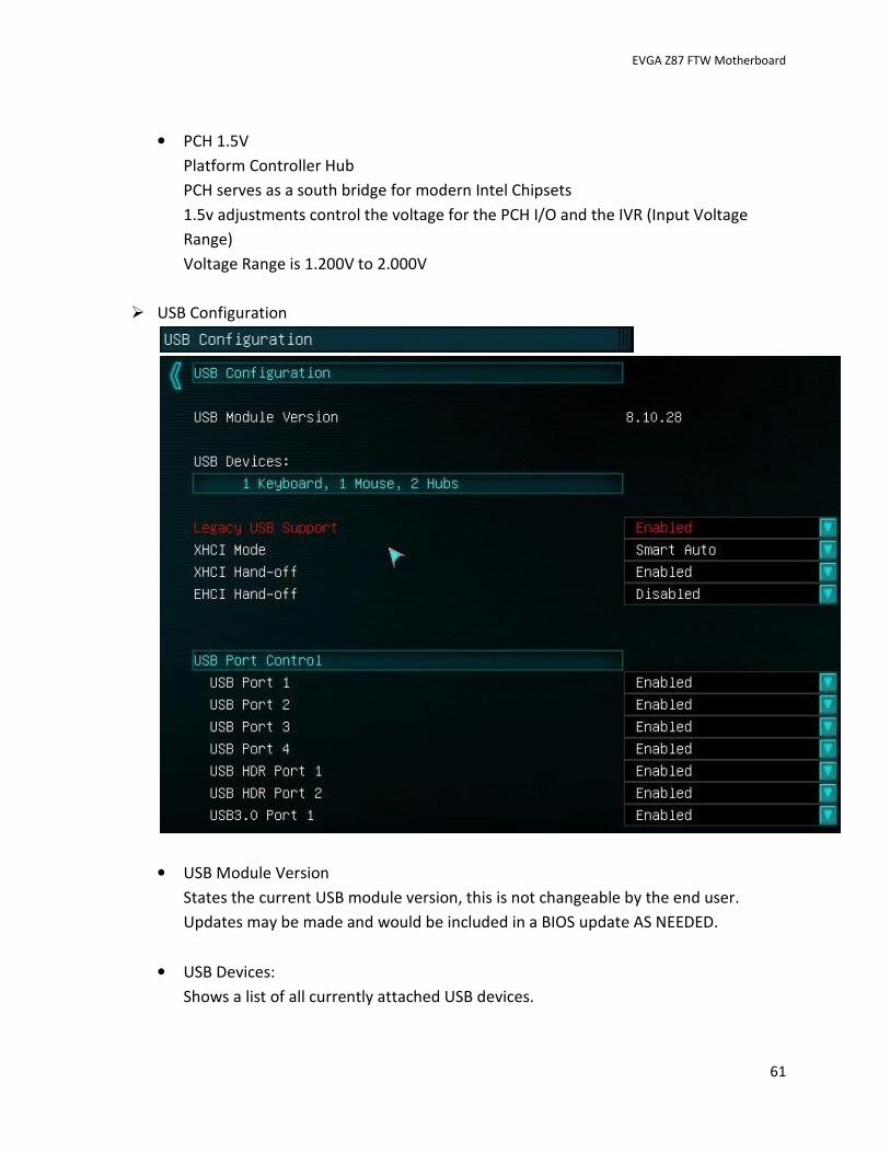
� USB Configuration
• USB Module Version
States the current USB module version, this is not changeable by the end user.
Updates may be made and would be included in a BIOS update AS NEEDED.
• USB Devices:
Shows a list of all currently attached USB devices.

EVGA Z87 FTW Motherboard
62
• Legacy USB Support
Enable/Disable/Auto
If this is disabled it will only support EFI compliant USB devices.
• XHCI Mode
eXtensible Host Controller Interface
Smart Auto/Auto/Enabled/Disabled
The most current mode for USB with several new features for functionality and
power saving. The xHCI architecture was designed to support all USB speeds,
including SuperSpeed (5 Gb/s) and future speeds, under a single driver stack.
• XHCI Hand-off
eXtensible Host Controller Interface
Enable/Disable
This is a workaround for OS’s without XHCI hand-off support. The XHCI ownership
change should be claimed by the XHCI driver.
• EHCI Hand-off
Enhanced Host Controller Interface
Compatibility mode for the high speed controller standard applicable to USB 2.0
• USB Port 1
Enable/Disable
• USB Port 2
Enable/Disable
• USB Port 3
Enable/Disable
• USB Port 4
Enable/Disable
• USB HDR Port 1
Enable/Disable
• USB HDR Port 2
Enable/Disable
EVGA Z87 FTW Motherboard
63
• USB3.0 Port 1
Enable/Disable
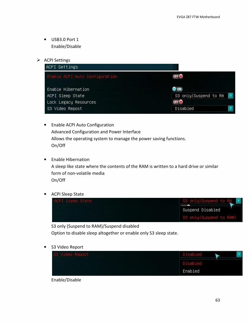
� ACPI Settings
• Enable ACPI Auto Configuration
Advanced Configuration and Power Interface
Allows the operating system to manage the power saving functions.
On/Off
• Enable Hibernation
A sleep like state where the contents of the RAM is written to a hard drive or similar
form of non-volatile media
On/Off
• ACPI Sleep State
S3 only (Suspend to RAM)/Suspend disabled
Option to disable sleep altogether or enable only S3 sleep state.
• S3 Video Report
Enable/Disable
EVGA Z87 FTW Motherboard
64
Re-initializes the video BIOS after waking up from an S3 sleep. This is to help with
the possible error when resuming that prevents video from re-enabling.
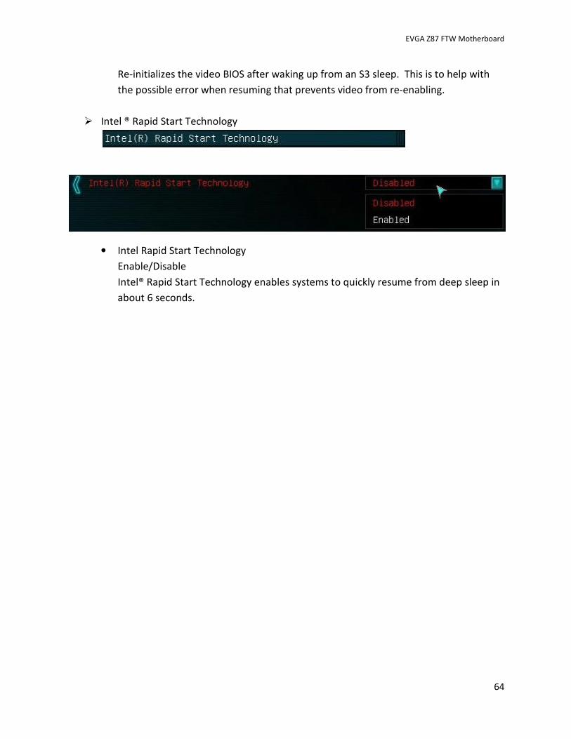
� Intel ® Rapid Start Technology
• Intel Rapid Start Technology
Enable/Disable
Intel® Rapid Start Technology enables systems to quickly resume from deep sleep in
about 6 seconds.
EVGA Z87 FTW Motherboard
65
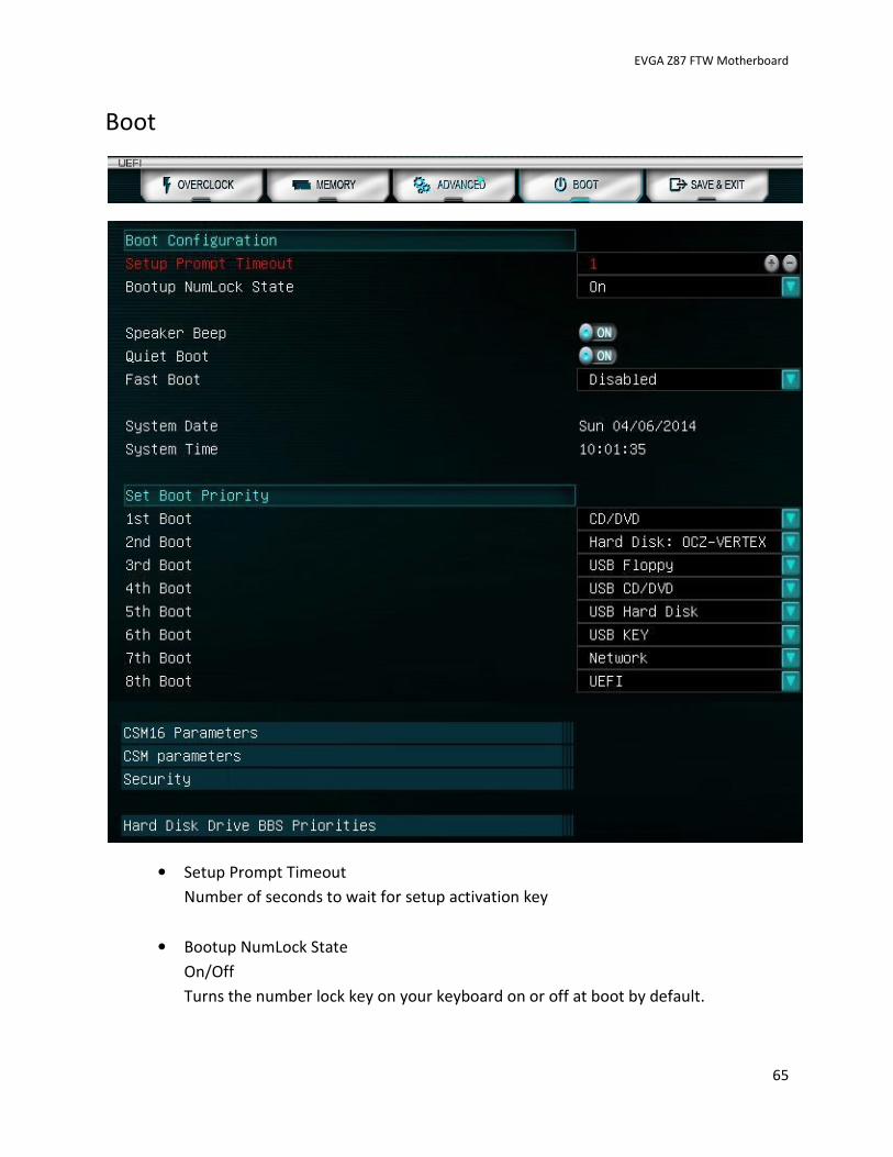
Boot
• Setup Prompt Timeout
Number of seconds to wait for setup activation key
• Bootup NumLock State
On/Off
Turns the number lock key on your keyboard on or off at boot by default.

EVGA Z87 FTW Motherboard
66
• Speaker Beep
On/Off
Allows using the PC Speaker for POST Beeps.
• Quiet Boot
On/Off
This enables or disables the splash screen during post.
• Fast Boot
Enable/Disable
Enabling Fast boot will make the initial post/boot slightly faster by bypassing the
boot device check and using last boot HDD.
• System Date
Displays today’s Date
• System Time
Displays Current Time
All 8 options below will share the same boot option list, and displays all detected devices
currently plugged into your PC. The list will look similar to this image:
• 1st
through 8th
Boot
Pick from the list from first down to create your boot order.

EVGA Z87 FTW Motherboard
67
� CSM 16 Parameters
Compatibility Support Module
CSM is a part of UEFI that offers backwards compatibility for older BIOS functions and
Option ROMs.
• CSM16 Module Version
States the version of the module.
• GateA20 Active
Gate A20 was for memory addressing in VERY old platforms, from 8 and 16 bit OS
era. Support for the A20 gate was changed in the Nehalem micro-architecture.
Rather than the CPU having a dedicated A20M# pin which receives the signal
whether or not to mask the A20 bit, this has been virtualized so that the information
is sent from the peripheral hardware to the CPU using special bus cycles. From a
software point-of-view, the mechanism works exactly as before, and an operating
system must still program external hardware (which in-turn sends the
aforementioned bus cycles to the CPU) to disable the A20 masking.
Upon Request/Always
• Option ROM Messages
This is the display mode for Option ROM
Force BIOS/Keep Current
• INT19 Trap Response
INIT19 is the decimal value for interrupt 0x13, which controls option ROM interface.
Immediate/Postponed
Immediate will launch this function during post; postponed will be during Legacy
Boot.
EVGA Z87 FTW Motherboard
68
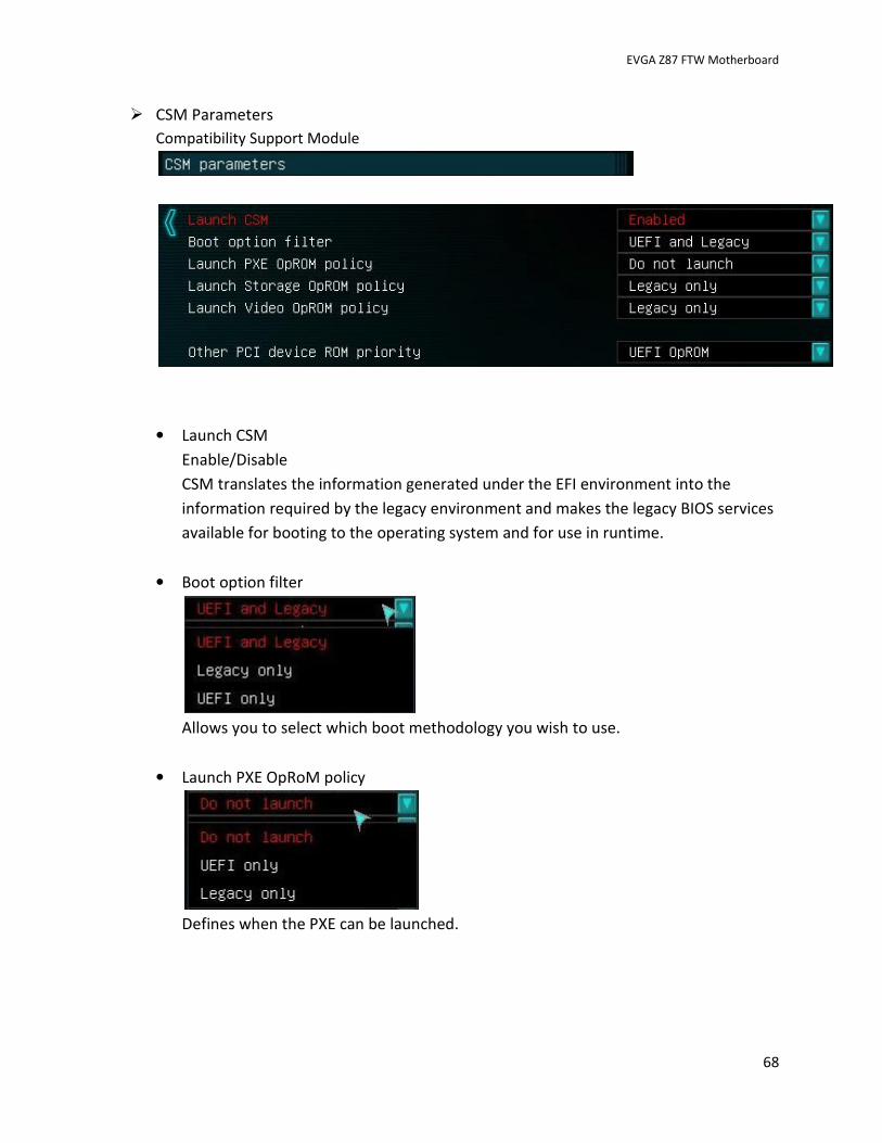
� CSM Parameters
Compatibility Support Module
• Launch CSM
Enable/Disable
CSM translates the information generated under the EFI environment into the
information required by the legacy environment and makes the legacy BIOS services
available for booting to the operating system and for use in runtime.
• Boot option filter
Allows you to select which boot methodology you wish to use.
• Launch PXE OpRoM policy
Defines when the PXE can be launched.

EVGA Z87 FTW Motherboard
69
• Launch Video OpROM policy
Selects when the video OpROM is initialized.
• Other PCI device ROM priority
Selects whether other OpROM’s will be initialized in UEFI Mode or Legacy Mode.
� Security
EVGA Z87 FTW Motherboard
70
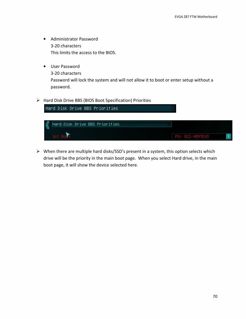
• Administrator Password
3-20 characters
This limits the access to the BIOS.
• User Password
3-20 characters
Password will lock the system and will not allow it to boot or enter setup without a
password.
� Hard Disk Drive BBS (BIOS Boot Specification) Priorities
� When there are multiple hard disks/SSD’s present in a system, this option selects which
drive will be the priority in the main boot page. When you select Hard drive, in the main
boot page, it will show the device selected here.
EVGA Z87 FTW Motherboard
71
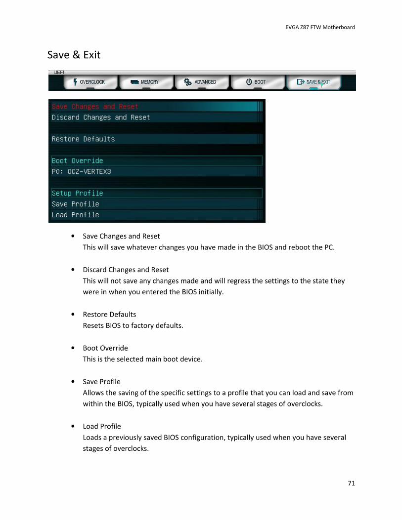
Save & Exit
• Save Changes and Reset
This will save whatever changes you have made in the BIOS and reboot the PC.
• Discard Changes and Reset
This will not save any changes made and will regress the settings to the state they
were in when you entered the BIOS initially.
• Restore Defaults
Resets BIOS to factory defaults.
• Boot Override
This is the selected main boot device.
• Save Profile
Allows the saving of the specific settings to a profile that you can load and save from
within the BIOS, typically used when you have several stages of overclocks.
• Load Profile
Loads a previously saved BIOS configuration, typically used when you have several
stages of overclocks.