Embed Size (px)
Citation preview

January 2012 Altera Corporation
CF52005-3.0
© 2012 Altera Corporation. AlQUARTUS and STRATIX worOffice and in other countries. Arespective holders as describedproducts to current specificatioproducts and services at any tiof any information, product, oradvised to obtain the latest verfor products or services.
101 Innovation DriveSan Jose, CA 95134www.altera.com
Configuration Devices for SRAM-BasedLUT Devices
Datasheet
This datasheet describes configuration devices for SRAM-based look-up table (LUT) devices.
Supported DevicesTable 1 lists the supported Altera configuration devices.
FeaturesConfiguration devices for SRAM-based LUT devices offer the following features:
■ Configures Altera ACEX 1K, APEX 20K (including APEX 20K, APEX 20KC, and APEX 20KE), APEX II, Arria GX, Cyclone, Cyclone II, FLEX 10K (including FLEX 10KE and FLEX 10KA) Mercury, Stratix, Stratix GX, Stratix II, and Stratix II GX devices
■ Easy-to-use four-pin interface
■ Low current during configuration and near-zero standby mode current
■ Programming support with the Altera Programming Unit (APU) and programming hardware from Data I/O, BP Microsystems, and other third-party programmers
■ Available in compact plastic packages
■ 8-pin plastic dual in-line (PDIP) package
■ 20-pin plastic J-lead chip carrier (PLCC) package
■ 32-pin plastic thin quad flat pack (TQFP) package
■ EPC2 device has reprogrammable flash configuration memory
Table 1. Altera Configuration Devices
Device Memory Size (Bits) ISP Support Cascaded Support Reprogrammable Recommended
Operating Voltage (V)
EPC1 1,046,496 No Yes No 5.0 or 3.3
EPC2 1,695,680 Yes Yes Yes 5.0 or 3.3
EPC1064 65,536 No No No 5.0
EPC1064V 65,536 No No No 3.3
EPC1213 212,942 No Yes No 5.0
EPC1441 440,800 No No No 5.0 or 3.3
l rights reserved. ALTERA, ARRIA, CYCLONE, HARDCOPY, MAX, MEGACORE, NIOS, ds and logos are trademarks of Altera Corporation and registered in the U.S. Patent and Trademark
ll other words and logos identified as trademarks or service marks are the property of their at www.altera.com/common/legal.html. Altera warrants performance of its semiconductor ns in accordance with Altera's standard warranty, but reserves the right to make changes to any
me without notice. Altera assumes no responsibility or liability arising out of the application or use service described herein except as expressly agreed to in writing by Altera. Altera customers are sion of device specifications before relying on any published information and before placing orders
Subscribe
ISO 9001:2008 Registered
Page 2 Functional Description
■ 5.0-V and 3.3-V in-system programmability (ISP) through the built-in IEEE Std. 1149.1 JTAG interface
■ Built-in JTAG boundary-scan test (BST) circuitry compliant with IEEE Std. 1149.1
■ Supports programming through Serial Vector Format File (.svf), Jam Standard Test and Programming Language (STAPL) Format File (.jam), JAM Byte Code File (.jbc), and the Quartus II and MAX+PLUS II softwares using the USB-Blaster, MasterBlaster, ByteBlaster II, EthernetBlaster, or ByteBlasterMV download cable
■ Supports programming through Programmer Object File (.pof) for EPC1 and EPC1441 devices
■ nINIT_CONF pin allows INIT_CONF JTAG instruction to begin FPGA configuration
f For more information about enhanced configuration (EPC) devices, refer to the Enhanced Configuration (EPC) Devices Datasheet.
f For more information about serial configuration (EPCS) devices, refer to the Serial Configuration (EPCS) Devices Datasheet.
Functional DescriptionWith SRAM-based devices, configuration data must be reloaded each time the device powers up, the system initializes, or when new configuration data is needed. Altera configuration devices store configuration data for SRAM-based ACEX 1K, APEX 20K, APEX II, Arria GX, Cyclone, Cyclone II, FLEX 10K, FLEX 6000, Mercury, Stratix, Stratix GX, Stratix II, and Stratix II GX devices.
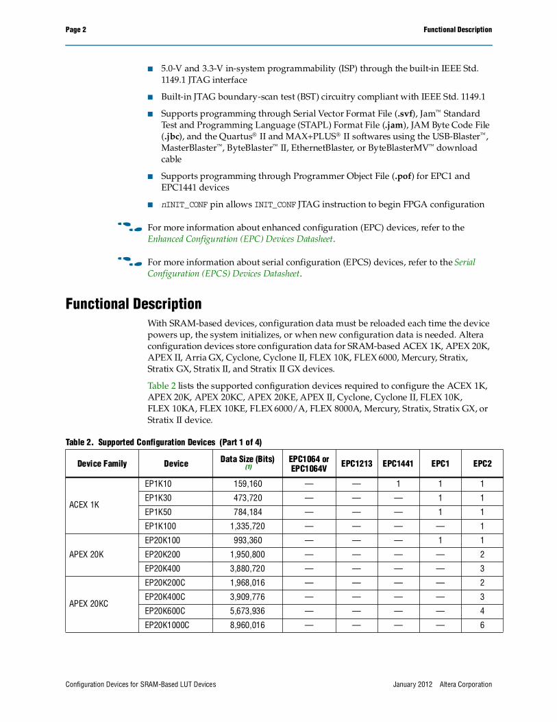
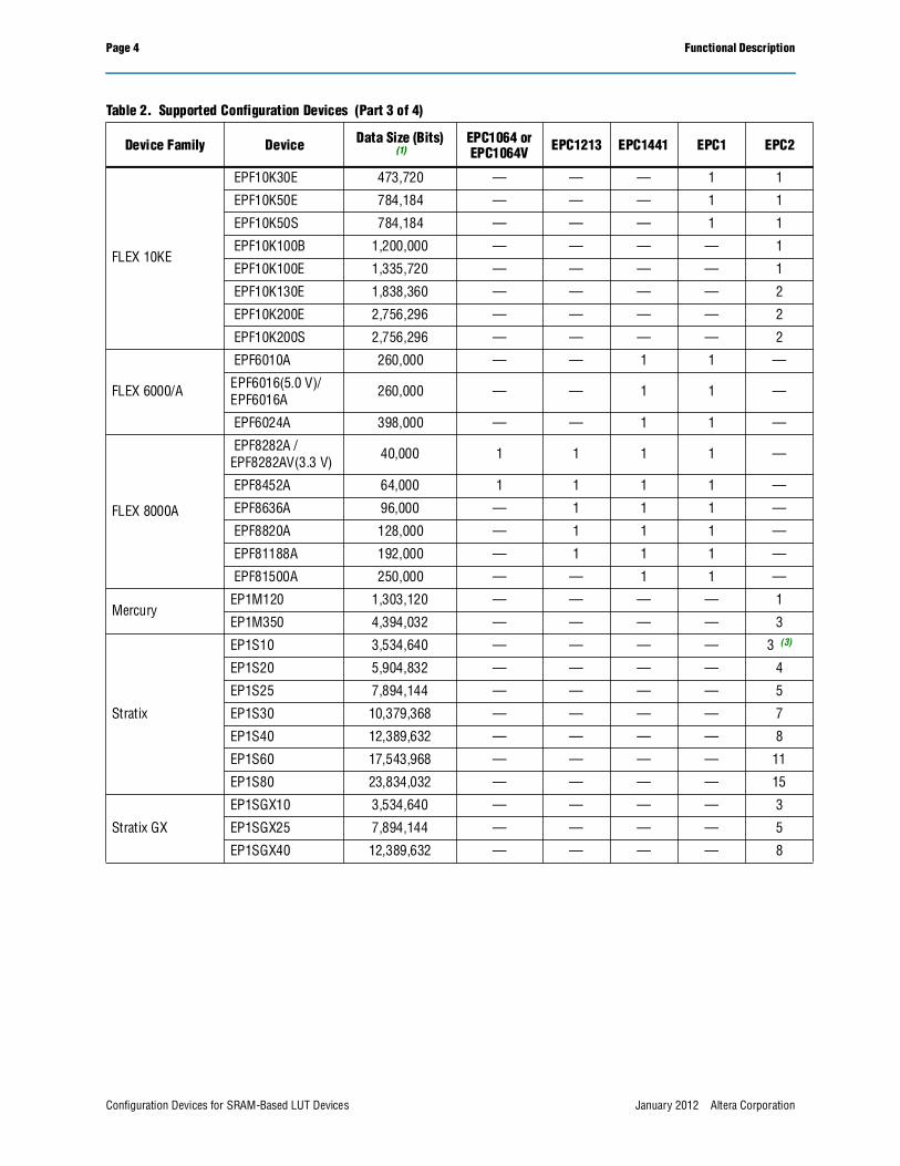
Table 2 lists the supported configuration devices required to configure the ACEX 1K, APEX 20K, APEX 20KC, APEX 20KE, APEX II, Cyclone, Cyclone II, FLEX 10K, FLEX 10KA, FLEX 10KE, FLEX 6000/A, FLEX 8000A, Mercury, Stratix, Stratix GX, or Stratix II device.
Table 2. Supported Configuration Devices (Part 1 of 4)
Device Family Device Data Size (Bits) (1)
EPC1064 or EPC1064V EPC1213 EPC1441 EPC1 EPC2
ACEX 1K
EP1K10 159,160 — — 1 1 1
EP1K30 473,720 — — — 1 1
EP1K50 784,184 — — — 1 1
EP1K100 1,335,720 — — — — 1
APEX 20K
EP20K100 993,360 — — — 1 1
EP20K200 1,950,800 — — — — 2
EP20K400 3,880,720 — — — — 3
APEX 20KC
EP20K200C 1,968,016 — — — — 2
EP20K400C 3,909,776 — — — — 3
EP20K600C 5,673,936 — — — — 4
EP20K1000C 8,960,016 — — — — 6
Configuration Devices for SRAM-Based LUT Devices January 2012 Altera Corporation

Functional Description Page 3
APEX 20KE
EP20K30E 354,832 — — 1 1 1
EP20K60E 648,016 — — — 1 1
EP20K100E 1,008,016 — — — 1 1
EP20K160E 1,524,016 — — — — 1
EP20K200E 1,968,016 — — — — 2
EP20K300E 2,741,616 — — — — 2
EP20K400E 3,909,776 — — — — 3
EP20K600E 5,673,936 — — — — 4
EP20K1000E 8,960,016 — — — — 6
EP20K1500E 12,042,256 — — — — 8
APEX II
EP2A15 1,168,688 — — — — 3
EP2A25 1,646,544 — — — — 4
EP2A40 2,543,016 — — — — 6
EP2A70 4,483,064 — — — — 11
Cyclone
EP1C3 627,376 — — — 1 1
EP1C4 925,000 — — — 1 1
EP1C6 1,167,216 — — — 1 (2) 1
EP1C12 2,326,528 — — — — 1 (2)
EP1C20 3,559,608 — — — — 2 (2)
Cyclone II
EP2C5 1,265,792 — — — — 1
EP2C8 1,983,536 — — — — 2
EP2C20 3,892,496 — — — — 3
EP2C35 6,848,608 — — — — 5
EP2C50 9,951,104 — — — — 6
EP2C70 14,319,216 — — — — 9
FLEX 10K
EPF10K10 118,000 — — 1 1 1
EPF10K20 231,000 — — 1 1 1
EPF10K30 376,000 — — 1 1 1
EPF10K40 498,000 — — — 1 1
EPF10K50 621,000 — — — 1 1
EPF10K70 892,000 — — — 1 1
EPF10K100 1,200,000 — — — — 1
FLEX 10KA
EPF10K10A 120,000 — — 1 1 1
EPF10K30A 406,000 — — 1 1 1
EPF10K50V 621,000 — — — 1 1
EPF10K100A 1,200,000 — — — — 1
EPF10K130V 1,600,000 — — — — 1
EPF10K250A 3,300,000 — — — — 2
Table 2. Supported Configuration Devices (Part 2 of 4)
Device Family Device Data Size (Bits) (1)
EPC1064 or EPC1064V EPC1213 EPC1441 EPC1 EPC2
Configuration Devices for SRAM-Based LUT DevicesJanuary 2012 Altera Corporation
Page 4 Functional Description
FLEX 10KE
EPF10K30E 473,720 — — — 1 1
EPF10K50E 784,184 — — — 1 1
EPF10K50S 784,184 — — — 1 1
EPF10K100B 1,200,000 — — — — 1
EPF10K100E 1,335,720 — — — — 1
EPF10K130E 1,838,360 — — — — 2
EPF10K200E 2,756,296 — — — — 2
EPF10K200S 2,756,296 — — — — 2
FLEX 6000/A
EPF6010A 260,000 — — 1 1 —
EPF6016(5.0 V)/ EPF6016A
260,000 — — 1 1 —
EPF6024A 398,000 — — 1 1 —
FLEX 8000A
EPF8282A / EPF8282AV(3.3 V)
40,000 1 1 1 1 —
EPF8452A 64,000 1 1 1 1 —
EPF8636A 96,000 — 1 1 1 —
EPF8820A 128,000 — 1 1 1 —
EPF81188A 192,000 — 1 1 1 —
EPF81500A 250,000 — — 1 1 —
MercuryEP1M120 1,303,120 — — — — 1
EP1M350 4,394,032 — — — — 3
Stratix
EP1S10 3,534,640 — — — — 3 (3)
EP1S20 5,904,832 — — — — 4
EP1S25 7,894,144 — — — — 5
EP1S30 10,379,368 — — — — 7
EP1S40 12,389,632 — — — — 8
EP1S60 17,543,968 — — — — 11
EP1S80 23,834,032 — — — — 15
Stratix GX
EP1SGX10 3,534,640 — — — — 3
EP1SGX25 7,894,144 — — — — 5
EP1SGX40 12,389,632 — — — — 8
Table 2. Supported Configuration Devices (Part 3 of 4)
Device Family Device Data Size (Bits) (1)
EPC1064 or EPC1064V EPC1213 EPC1441 EPC1 EPC2
Configuration Devices for SRAM-Based LUT Devices January 2012 Altera Corporation

Functional Description Page 5
Figure 1 shows the configuration device block diagram.
Stratix II
EP2S15 5,000,000 — — — — 3
EP2S30 10,100,000 — — — — 7
EP2S60 17,100,000 — — — — 11
EP2S90 27,500,000 — — — — 17
EP2S130 39,600,000 — — — — 24
EP2S180 52,400,000 — — — — 31
Notes to Table 2:
(1) Raw Binary File (.rbf) were used to determine these sizes.(2) This number is calculated with the Cyclone series compression feature enabled.(3) EP1S10 ES devices requires four EPC2 devices.
Table 2. Supported Configuration Devices (Part 4 of 4)
Device Family Device Data Size (Bits) (1)
EPC1064 or EPC1064V EPC1213 EPC1441 EPC1 EPC2
Figure 1. Configuration Device Block Diagram
Notes to Figure 1:
(1) The EPC1441 devices do not support data cascading. The EPC1, EPC2, and EPC1213 devices support data cascading.(2) The OE pin is a bidirectional open-drain pin.
DCLK
nCS
OE
DecodeLogic
Address
DATA
DATAShiftRegister
EPROMArray
nCS
DecodeLogic
Address
Oscillator
OscillatorControl
EPROMArray
ShiftRegister
DATA
DATA
DCLK
nCASC
nCASC
(1)
(1)
FPGA (except FLEX 8000) Configuration Using an EPC2, EPC1, or EPC1441
FLEX 8000 Device Configuration Using an EPC1, EPC1441, EPC1213, EPC1064, or EPC1064V
AddressCounter
CLKENAnRESET
ErrorDetectionCircuitryOE
AddressCounter
CLKENAnRESET
(2)
Configuration Devices for SRAM-Based LUT DevicesJanuary 2012 Altera Corporation

Page 6 Device Configuration
Device ConfigurationThe EPC1, EPC2, and EPC1441 devices store configuration data in its erasable programmable read-only memory (EPROM) array and serially clock data out using an internal oscillator. The OE, nCS, and DCLK pins supply the control signals for the address counter and the DATA output tri-state buffer. The configuration device sends a serial bitstream of configuration data to its DATA pin, which is routed to the DATA0 input of the FPGA.
The control signals for configuration devices, OE, nCS, and DCLK, interface directly with the FPGA control signals, nSTATUS, CONF_DONE, and DCLK. All Altera FPGAs can be configured by a configuration device without requiring an external intelligent controller.
1 An EPC2 device cannot configure FLEX 8000 or FLEX 6000 devices. For configuration devices that support FLEX 8000 or FLEX 6000 devices, refer to Table 2.
Figure 2 shows the basic configuration interface connections between the configuration device and the Altera FPGA.
The EPC2 device allows you to begin configuration of the FPGA using an additional pin, nINIT_CONF. The nINIT_CONF pin of the EPC2 device can be connected to the nCONFIG pin of the FPGA, which allows the INIT_CONF JTAG instruction to begin FPGA configuration. The INIT_CONF JTAG instruction causes the EPC2 device to drive the nINIT_CONF pin low, which in turn pulls the nCONFIG pin low. Pulling the nCONFIG pin low on the FPGA will reset the device. When the JTAG state machine exits this state, the nINIT_CONF pin is released and pulled high by an internal 1-k resistor, which in turn pulls the nCONFIG pin high to begin configuration. If you do not use the nINIT_CONF pin, disconnect the nINIT_CONF pin, and pull the nCONFIG pin of the FPGA to VCC either directly or through a resistor.
Figure 2. Altera FPGA Configured Using an EPC1, EPC2, or EPC1441 Configuration Device (1)
Notes to Figure 2:(1) For more information about configuration interface connections, refer to the configuration chapter in the appropriate device handbook.(2) The nINIT_CONF pin which is available on EPC2 devices has an internal pull-up resistor that is always active. This means an external pull-up
resistor is not required on the nINIT_CONF/nCONFIG line. The nINIT_CONF pin does not need to be connected if its functionality is not used. If the nINIT_CONF pin is not used or unavailable, nCONFIG must be pulled to VCC either directly or through a resistor.
(3) EPC2 devices have internal programmable pull-up resistors on OE and nCS pins. If internal pull-up resistors are used, do not use external pull-up resistors on these pins. The internal pull-up resistors are set by default in the Quartus II software. To turn off the internal pull-up resistors, check the Disable nCS and OE pull-ups on configuration device option when you generate programming files.
FPGAConfiguration
DeviceDCLKDATAOE (3)nCS (3)nINIT_CONF (2)
MSEL
DCLKDATA0
nSTATUSCONF_DONE
nCONFIG
VCC VCC
GND
nCE
VCC
nCEO
nCASC N.C.
N.C.
n
(2)(3) (3)
Configuration Devices for SRAM-Based LUT Devices January 2012 Altera Corporation
Device Configuration Page 7
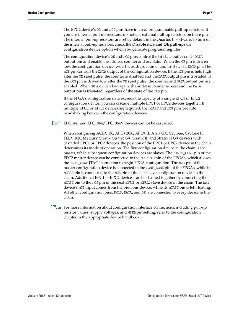
The EPC2 device’s OE and nCS pins have internal programmable pull-up resistors. If you use internal pull-up resistors, do not use external pull-up resistors on these pins. The internal pull-up resistors are set by default in the Quartus II software. To turn off the internal pull-up resistors, check the Disable nCS and OE pull-ups on configuration device option when you generate programming files.
The configuration device’s OE and nCS pins control the tri-state buffer on its DATA output pin and enable the address counter and oscillator. When the OE pin is driven low, the configuration device resets the address counter and tri-states its DATA pin. The nCS pin controls the DATA output of the configuration device. If the nCS pin is held high after the OE reset pulse, the counter is disabled and the DATA output pin is tri-stated. If the nCS pin is driven low after the OE reset pulse, the counter and DATA output pin are enabled. When OE is driven low again, the address counter is reset and the DATA output pin is tri-stated, regardless of the state of the nCS pin.
If the FPGA’s configuration data exceeds the capacity of a single EPC1 or EPC2 configuration device, you can cascade multiple EPC1 or EPC2 devices together. If multiple EPC1 or EPC2 devices are required, the nCASC and nCS pins provide handshaking between the configuration devices.
1 EPC1441 and EPC1064/EPC1064V devices cannot be cascaded.
When configuring ACEX 1K, APEX 20K, APEX II, Arria GX, Cyclone, Cyclone II, FLEX 10K, Mercury, Stratix, Stratix GX, Stratix II, and Stratix II GX devices with cascaded EPC1 or EPC2 devices, the position of the EPC1 or EPC2 device in the chain determines its mode of operation. The first configuration device in the chain is the master, while subsequent configuration devices are slaves. The nINIT_CONF pin of the EPC2 master device can be connected to the nCONFIG pin of the FPGAs, which allows the INIT_CONF JTAG instruction to begin FPGA configuration. The nCS pin of the master configuration device is connected to the CONF_DONE pin of the FPGAs, while its nCASC pin is connected to the nCS pin of the next slave configuration device in the chain. Additional EPC1 or EPC2 devices can be chained together by connecting the nCASC pin to the nCS pin of the next EPC1 or EPC2 slave device in the chain. The last device’s nCS input comes from the previous device, while its nCASC pin is left floating. All other configuration pins, DCLK, DATA, and OE, are connected to every device in the chain.
f For more information about configuration interface connections, including pull-up resistor values, supply voltages, and MSEL pin setting, refer to the configuration chapter in the appropriate device handbook.
Configuration Devices for SRAM-Based LUT DevicesJanuary 2012 Altera Corporation

Page 8 Device Configuration
Figure 3 shows the basic configuration interface connections between a configuration device chain and the Altera FPGA.
When the first device in a configuration device chain is powered-up or reset, its nCS pin is driven low because it is connected to the CONF_DONE pin of the FPGA. Because both OE and nCS pins are low, the first device in the chain recognizes it as the master device and controls configuration. Since the slave devices’ nCS pin is fed by the previous devices’ nCASC pin, its nCS pin is high after power-up and reset. In the slave configuration devices, the DATA output is tri-stated and DCLK is an input. During configuration, the master device supplies the clock through DCLK to the FPGA and to any slave configuration devices. The EPC1 or EPC2 master device also provides the first stream of data to the FPGA during multi-device configuration. After the EPC1 or EPC2 master device finishes sending configuration data, it tri-states its DATA pin to avoid contention with other configuration devices. The EPC1 or EPC2 master device also drives its nCASC pin low, which pulls the nCS pin of the next device low. This action signals the EPC1 or EPC2 slave device to start sending configuration data to the FPGAs.
The EPC1 or EPC2 master device clocks all slave configuration devices until configuration is complete. When all configuration data is transferred and the nCS pin on the EPC1 or EPC2 master device is driven high by the FPGA’s CONF_DONE pin, the EPC1 or EPC2 master device then goes into zero-power (idle) state. The EPC2 master device drives DATA high and DCLK low, while the EPC1 and EPC1441 device tri-state DATA and drive DCLK low.
If the nCS pin on the EPC1 or EPC2 master device is driven high before all configuration data is transferred, the EPC1 or EPC2 master device drives its OE signal low, which in turn drives the FPGA’s nSTATUS pin low, indicating a configuration error. Additionally, if the configuration device generates its data and detects that the CONF_DONE pin has not gone high, it recognizes that the FPGA has not configured successfully. EPC1 and EPC2 devices wait for 16 DCLK cycles after the last
Figure 3. Altera FPGA Configured Using Two EPC1 or EPC2 Configuration Devices (1)
Notes to Figure 3:(1) For more information about configuration interface connections, refer to the configuration chapter in the appropriate device handbook.(2) The nINIT_CONF pin which is available on EPC2 devices has an internal pull-up resistor that is always active. This means an external pull-up
resistor is not required on the nINIT_CONF/nCONFIG line. The nINIT_CONF pin does not need to be connected if its functionality is not used. If the nINIT_CONF pin is not used or unavailable, nCONFIG must be pulled to VCC either directly or through a resistor.
(3) EPC2 devices have internal programmable pull-up resistors on OE and nCS pins. If internal pull-up resistors are used, do not use external pull-up resistors on these pins. The internal pull-up resistors are set by default in the Quartus II software. To turn off the internal pull-up resistors, check the Disable nCS and OE pull-ups on configuration device option when you generate programming files.
VCCVCC
GND
DCLKDATAnCSOE
FPGA
MSEL
DCLKDATA0
nSTATUSCONF_DONE
nCONFIG
nCE
MasterConfiguration
Device
SlaveConfiguration
DeviceDCLKDATAOE (3)nCS (3) nINIT_CONF (2)
nCASC nCASC N.C.
nCEO N.C.
VCC
(2)(3) (3)
n
Configuration Devices for SRAM-Based LUT Devices January 2012 Altera Corporation

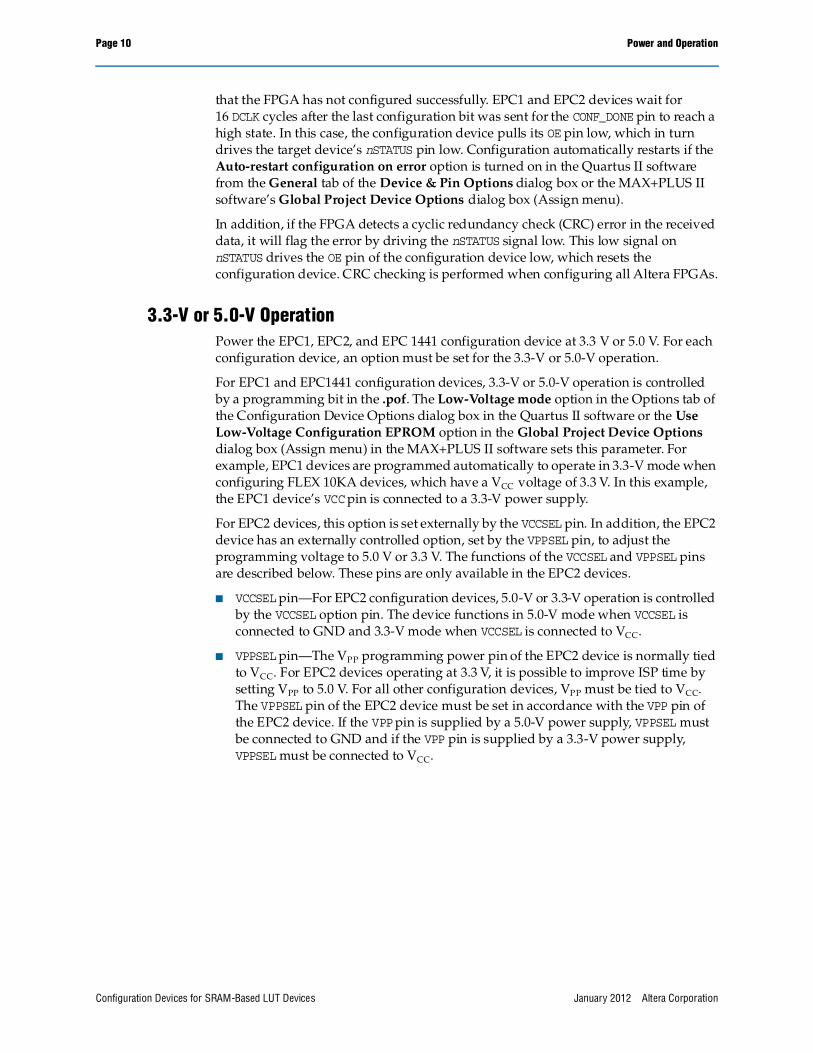
Power and Operation Page 9
configuration bit was sent for the CONF_DONE pin to reach a high state. In this case, the configuration device pulls its OE pin low, which in turn drives the target device’s nSTATUS pin low. Configuration automatically restarts if the Auto-restart configuration on error option is turned on in the Quartus II software from the General tab of the Device & Pin Options dialog box or the MAX+PLUS II software’s Global Project Device Options dialog box (Assign menu).
f For more information about FPGA configuration and configuration interface connections between configuration devices and Altera FPGAs, refer to the configuration chapter in the appropriate device handbook.
Power and OperationThis section describes power-on reset (POR) delay, error detection, and 3.3-V and 5.0-V operation of Altera configuration devices.
Power-On ResetDuring initial power-up, a POR delay occurs to permit voltage levels to stabilize. When configuring an FPGA with one EPC1, EPC2, or EPC1441 device, the POR delay occurs inside the configuration device and the POR delay is a maximum of 200 ms. When configuring a FLEX 8000 device with one EPC1213, EPC1064, or EPC1064V device, the POR delay occurs inside the FLEX 8000 device and the POR delay is typically 100 ms, with a maximum of 200 ms.
During POR, the configuration device drives its OE pin low. This low signal delays configuration because the OE pin is connected to the target FPGA’s nSTATUS pin. When the configuration device completes POR, it releases its open-drain OE pin, which is then pulled high by a pull-up resistor.
1 You should power up the FPGA before the configuration device exits POR to avoid the master configuration device from entering slave mode.
If the FPGA is not powered up before the configuration device exits POR, the CONF_DONE/nCS line is high because of the pull-up resistor. When the configuration device exits POR and releases OE, it sees nCS high, which signals the configuration device to enter slave mode. Therefore, configuration will not begin because the DATA output is tri-stated and DCLK is an input pin in slave mode.
Error Detection CircuitryThe EPC1, EPC2, and EPC1441 configuration devices have built-in error detection circuitry for configuring ACEX 1K, APEX 20K, APEX II, Arria GX, Cyclone, Cyclone II, FLEX 10K, FLEX 6000, Mercury, Stratix, Stratix GX, Stratix II, or Stratix II GX devices.
Built-in error detection circuitry uses the nCS pin of the configuration device, which monitors the CONF_DONE pin on the FPGA. If the nCS pin on the EPC1 or EPC2 master device is driven high before all configuration data is transferred, the EPC1 or EPC2 master device drives its OE signal low, which in turn drives the FPGA’s nSTATUS pin low, indicating a configuration error. Additionally, if the configuration device generates its data and detects that the CONF_DONE pin has not gone high, it recognizes
Configuration Devices for SRAM-Based LUT DevicesJanuary 2012 Altera Corporation
Page 10 Power and Operation
that the FPGA has not configured successfully. EPC1 and EPC2 devices wait for 16 DCLK cycles after the last configuration bit was sent for the CONF_DONE pin to reach a high state. In this case, the configuration device pulls its OE pin low, which in turn drives the target device’s nSTATUS pin low. Configuration automatically restarts if the Auto-restart configuration on error option is turned on in the Quartus II software from the General tab of the Device & Pin Options dialog box or the MAX+PLUS II software’s Global Project Device Options dialog box (Assign menu).
In addition, if the FPGA detects a cyclic redundancy check (CRC) error in the received data, it will flag the error by driving the nSTATUS signal low. This low signal on nSTATUS drives the OE pin of the configuration device low, which resets the configuration device. CRC checking is performed when configuring all Altera FPGAs.
3.3-V or 5.0-V OperationPower the EPC1, EPC2, and EPC 1441 configuration device at 3.3 V or 5.0 V. For each configuration device, an option must be set for the 3.3-V or 5.0-V operation.
For EPC1 and EPC1441 configuration devices, 3.3-V or 5.0-V operation is controlled by a programming bit in the .pof. The Low-Voltage mode option in the Options tab of the Configuration Device Options dialog box in the Quartus II software or the Use Low-Voltage Configuration EPROM option in the Global Project Device Options dialog box (Assign menu) in the MAX+PLUS II software sets this parameter. For example, EPC1 devices are programmed automatically to operate in 3.3-V mode when configuring FLEX 10KA devices, which have a VCC voltage of 3.3 V. In this example, the EPC1 device’s VCC pin is connected to a 3.3-V power supply.
For EPC2 devices, this option is set externally by the VCCSEL pin. In addition, the EPC2 device has an externally controlled option, set by the VPPSEL pin, to adjust the programming voltage to 5.0 V or 3.3 V. The functions of the VCCSEL and VPPSEL pins are described below. These pins are only available in the EPC2 devices.
■ VCCSEL pin—For EPC2 configuration devices, 5.0-V or 3.3-V operation is controlled by the VCCSEL option pin. The device functions in 5.0-V mode when VCCSEL is connected to GND and 3.3-V mode when VCCSEL is connected to VCC.
■ VPPSEL pin—The VPP programming power pin of the EPC2 device is normally tied to VCC. For EPC2 devices operating at 3.3 V, it is possible to improve ISP time by setting VPP to 5.0 V. For all other configuration devices, VPP must be tied to VCC. The VPPSEL pin of the EPC2 device must be set in accordance with the VPP pin of the EPC2 device. If the VPP pin is supplied by a 5.0-V power supply, VPPSEL must be connected to GND and if the VPP pin is supplied by a 3.3-V power supply, VPPSEL must be connected to VCC.
Configuration Devices for SRAM-Based LUT Devices January 2012 Altera Corporation
Power and Operation Page 11
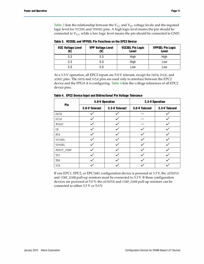
Table 3 lists the relationship between the VCC and VPP voltage levels and the required logic level for VCCSEL and VPPSEL pins. A high logic level means the pin should be connected to VCC, while a low logic level means the pin should be connected to GND.
At a 3.3-V operation, all EPC2 inputs are 5.0-V tolerant, except for DATA, DCLK, and nCASC pins. The DATA and DCLK pins are used only to interface between the EPC2 device and the FPGA it is configuring. Table 4 lists the voltage tolerences of all EPC2 device pins.
If one EPC1, EPC2, or EPC1441 configuration device is powered at 3.3 V, the nSTATUS and CONF_DONE pull-up resistors must be connected to 3.3 V. If these configuration devices are powered at 5.0 V, the nSTATUS and CONF_DONE pull-up resistors can be connected to either 3.3 V or 5.0 V.
Table 3. VCCSEL and VPPSEL Pin Functions on the EPC2 Device
VCC Voltage Level(V)
VPP Voltage Level(V)
VCCSEL Pin Logic Level
VPPSEL Pin Logic Level
3.3 3.3 High High
3.3 5.0 High Low
5.0 5.0 Low Low
Table 4. EPC2 Device Input and Bidirectional Pin Voltage Tolerance
Pin5.0-V Operation 3.3-V Operation
5.0-V Tolerant 3.3-V Tolerant 5.0-V Tolerant 3.3-V Tolerant
DATA v v — v
DCLK v v — v
nCASC v v — v
OE v v v v
nCS v v v v
VCCSEL v v v v
VPPSEL v v v v
nINIT_CONF v v v v
TDI v v v v
TMS v v v v
TCK v v v v
Configuration Devices for SRAM-Based LUT DevicesJanuary 2012 Altera Corporation
Page 12 Programming and Configuration File Support
Programming and Configuration File SupportThe Quartus II and MAX+PLUS II softwares provide programming support for Altera configuration devices. During compilation, the Quartus II and MAX+PLUS II softwares automatically generates a .pof, which is used to program the configuration devices. In a multi-device configuration, the software combines the programming files for multiple ACEX 1K, APEX 20K, APEX II, Arria GX, Cyclone, Cyclone II, FLEX 10K, Mercury, Stratix, Stratix GX, Stratix II, and Stratix II GX devices into one or more configuration devices. The software allows you to select the appropriate configuration device to store the data for each FPGA.
All Altera configuration devices are programmable using Altera programming hardware in conjunction with the Quartus II or MAX+PLUS II software. In addition, many third-party programmers offer programming hardware that supports Altera configuration devices.
1 An EPC2 device can be programmed with a .pof generated for an EPC1 or EPC1441 device. An EPC1 device can be programmed with a .pof generated for an EPC1441 device.
EPC2 configuration devices can be programmed in-system through its industry-standard four-pin JTAG interface. ISP capability in the EPC2 devices provide ease in prototyping and FPGA functionality. When programming multiple EPC2 devices in a JTAG chain, the Quartus II and MAX+PLUS II softwares and other programming methods employ concurrent programming to simultaneously program multiple devices and reduce programming time. EPC2 devices can be programmed and erased up to 100 times.
After programming an EPC2 device in-system, FPGA configuration is initiated by the INIT_CONF JTAG instruction of the EPC2 device. For more information, refer to Table 6.
f For more information about programming and configuration support, refer to the following documents:
■ Altera Programming Hardware Data Sheet
■ USB-Blaster Download Cable User Guide
■ MasterBlaster Serial/USB Communications Cable User Guide
■ ByteBlaster II Download Cable User Guide
■ ByteBlasterMV Download Cable User Guide
■ BitBlaster Serial Download Cable Data Sheet
You can also program the configuration devices using the Quartus II or MAX+PLUS II software with the APU or the appropriate configuration device programming adapter.
Configuration Devices for SRAM-Based LUT Devices January 2012 Altera Corporation

Programming and Configuration File Support Page 13
Table 5 lists the programming adapter to use with each configuration device.
To program Altera configuration devices using the Quartus II software and the APU, follow these steps:
1. Choose the Quartus II Programmer (Tools menu).
2. Load the appropriate .pof by clicking Add. The Device column displays the device for the current programming file.
3. Insert a blank configuration device into the programming adapter’s socket.
4. Turn on the Program/Configure. You can also turn on Verify to verify the contents of a programmed device against the programming data loaded from a programming file.
5. Click Start.
6. After successful programming, you can place the configuration device on the PCB to configure the FPGA device.
To program Altera configuration devices using the MAX+PLUS II software and the APU, follow these steps:
1. Open the MAX+PLUS II Programmer.
2. Load the appropriate .pof using the Select Programming File dialog box (File menu). By default, the Programmer loads the current project’s .pof. The Device field displays the device for the current programming file.
3. Insert a blank configuration device into the programming adapter’s socket.
4. Click Program.
5. After successful programming, you can place the configuration device on the PCB to configure the FPGA device.
If you are cascading EPC1 or EPC2 devices, you must generate multiple .pof. The first device .pof have the same name as the project, while the second device .pof have the same name as the first, but with a “_1” extension (e.g., top_1.pof).
Table 5. Programming Adapters
Device Package Adapter
EPC220-pin J-Lead PLMJ1213
32-pin TQFP PLMT1213
EPC18-pin DIP PLMJ1213
20-pin J-Lead PLMJ1213
EPC1441
8-pin DIP PLMJ1213
20-pin J-Lead PLMJ1213
32-pin TQFP PLMT1064
Configuration Devices for SRAM-Based LUT DevicesJanuary 2012 Altera Corporation
Page 14 IEEE Std. 1149.1 (JTAG) Boundary-Scan Testing
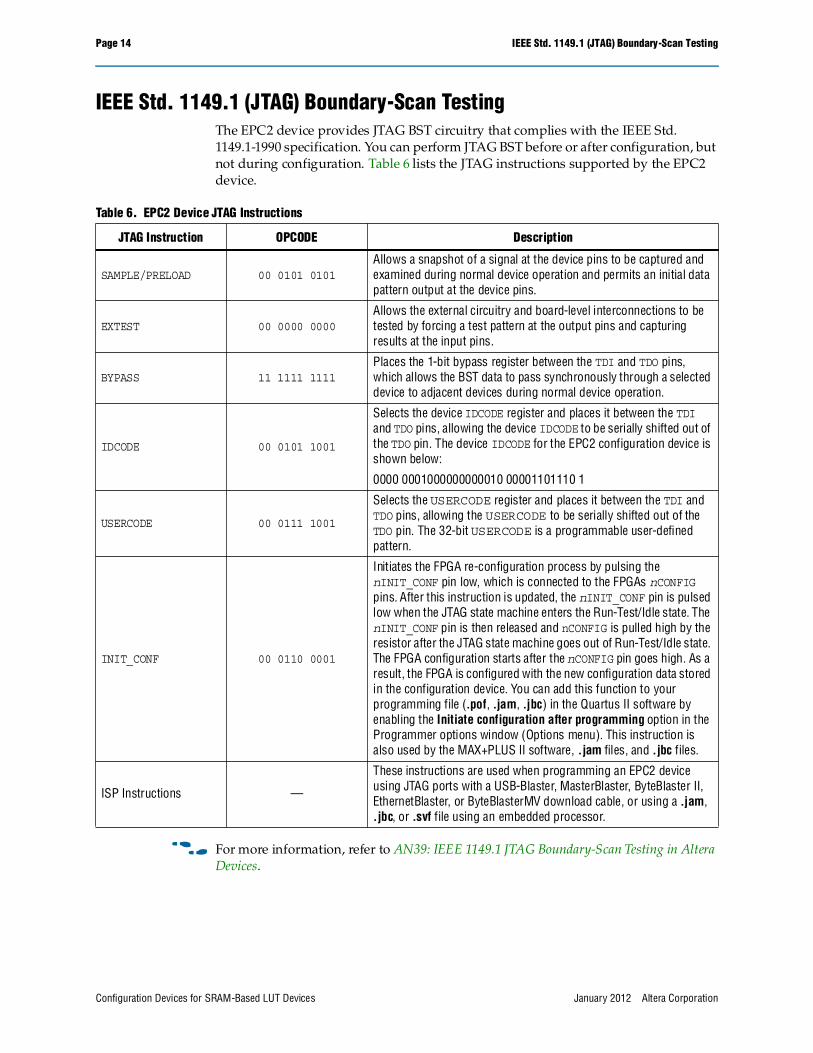
IEEE Std. 1149.1 (JTAG) Boundary-Scan TestingThe EPC2 device provides JTAG BST circuitry that complies with the IEEE Std. 1149.1-1990 specification. You can perform JTAG BST before or after configuration, but not during configuration. Table 6 lists the JTAG instructions supported by the EPC2 device.
f For more information, refer to AN39: IEEE 1149.1 JTAG Boundary-Scan Testing in Altera Devices.
Table 6. EPC2 Device JTAG Instructions
JTAG Instruction OPCODE Description
SAMPLE/PRELOAD 00 0101 0101Allows a snapshot of a signal at the device pins to be captured and examined during normal device operation and permits an initial data pattern output at the device pins.
EXTEST 00 0000 0000Allows the external circuitry and board-level interconnections to be tested by forcing a test pattern at the output pins and capturing results at the input pins.
BYPASS 11 1111 1111Places the 1-bit bypass register between the TDI and TDO pins, which allows the BST data to pass synchronously through a selected device to adjacent devices during normal device operation.
IDCODE 00 0101 1001
Selects the device IDCODE register and places it between the TDI and TDO pins, allowing the device IDCODE to be serially shifted out of the TDO pin. The device IDCODE for the EPC2 configuration device is shown below:
0000 0001000000000010 00001101110 1
USERCODE 00 0111 1001
Selects the USERCODE register and places it between the TDI and TDO pins, allowing the USERCODE to be serially shifted out of the TDO pin. The 32-bit USERCODE is a programmable user-defined pattern.
INIT_CONF 00 0110 0001
Initiates the FPGA re-configuration process by pulsing the nINIT_CONF pin low, which is connected to the FPGAs nCONFIG pins. After this instruction is updated, the nINIT_CONF pin is pulsed low when the JTAG state machine enters the Run-Test/Idle state. The nINIT_CONF pin is then released and nCONFIG is pulled high by the resistor after the JTAG state machine goes out of Run-Test/Idle state. The FPGA configuration starts after the nCONFIG pin goes high. As a result, the FPGA is configured with the new configuration data stored in the configuration device. You can add this function to your programming file (.pof, .jam, .jbc) in the Quartus II software by enabling the Initiate configuration after programming option in the Programmer options window (Options menu). This instruction is also used by the MAX+PLUS II software, .jam files, and .jbc files.
ISP Instructions —
These instructions are used when programming an EPC2 device using JTAG ports with a USB-Blaster, MasterBlaster, ByteBlaster II, EthernetBlaster, or ByteBlasterMV download cable, or using a .jam, .jbc, or .svf file using an embedded processor.
Configuration Devices for SRAM-Based LUT Devices January 2012 Altera Corporation

IEEE Std. 1149.1 (JTAG) Boundary-Scan Testing Page 15
Figure 4 shows the timing requirements for the JTAG signals.
Table 7 lists the timing parameters and values for configuration devices.
Figure 4. EPC2 Device JTAG Waveforms
Table 7. JTAG Timing Parameters and Values
Symbol Parameter Min Max Unit
tJCP TCK clock period 100 — ns
tJCH TCK clock high time 50 — ns
tJCL TCK clock low time 50 — ns
tJPSU JTAG port setup time 20 — ns
tJPH JTAG port hold time 45 — ns
tJPCO JTAG port clock to output — 25 ns
tJPZX JTAG port high impedance to valid output — 25 ns
tJPXZ JTAG port valid output to high impedance — 25 ns
tJSSU Capture register setup time 20 — ns
tJSH Capture register hold time 45 — ns
tJSCO Update register clock to output — 25 ns
tJSZX Update register high impedance to valid output — 25 ns
tJSXZ Update register valid output to high impedance — 25 ns
TDO
TCK
tJPZX tJPCO
tJPH
tJPXZ
tJCP
tJPSU tJCL tJCH
TDI
TMS
Signalto be
Captured
Signalto be
Driven
tJSZX
tJSSU tJSH
tJSCO tJSXZ
Configuration Devices for SRAM-Based LUT DevicesJanuary 2012 Altera Corporation
Page 16 Timing Information
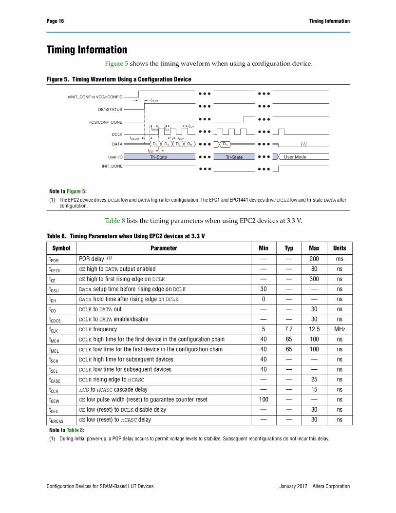
Timing InformationFigure 5 shows the timing waveform when using a configuration device.
Table 8 lists the timing parameters when using EPC2 devices at 3.3 V.
Figure 5. Timing Waveform Using a Configuration Device
Note to Figure 5:(1) The EPC2 device drives DCLK low and DATA high after configuration. The EPC1 and EPC1441 devices drive DCLK low and tri-state DATA after
configuration.
D D D D0 1 2 3 Dn
Tri-State User Mode
(1)tOEZX
tPOR
tCHtCLtDSU
tCO
tDH
Tri-State
OE/nSTATUS
nCS/CONF_DONE
DCLK
DATA
User I/O
INIT_DONE
nINIT_CONF or VCC/nCONFIG
Table 8. Timing Parameters when Using EPC2 devices at 3.3 V
Symbol Parameter Min Typ Max Units
tPOR POR delay (1) — — 200 ms
tOEZX OE high to DATA output enabled — — 80 ns
tCE OE high to first rising edge on DCLK — — 300 ns
tDSU Data setup time before rising edge on DCLK 30 — — ns
tDH Data hold time after rising edge on DCLK 0 — — ns
tCO DCLK to DATA out — — 30 ns
tCDOE DCLK to DATA enable/disable — — 30 ns
fCLK DCLK frequency 5 7.7 12.5 MHz
tMCH DCLK high time for the first device in the configuration chain 40 65 100 ns
tMCL DCLK low time for the first device in the configuration chain 40 65 100 ns
tSCH DCLK high time for subsequent devices 40 — — ns
tSCL DCLK low time for subsequent devices 40 — — ns
tCASC DCLK rising edge to nCASC — — 25 ns
tCCA nCS to nCASC cascade delay — — 15 ns
tOEW OE low pulse width (reset) to guarantee counter reset 100 — — ns
tOEC OE low (reset) to DCLK disable delay — — 30 ns
tNRCAS OE low (reset) to nCASC delay — — 30 ns
Note to Table 8:(1) During initial power-up, a POR delay occurs to permit voltage levels to stabilize. Subsequent reconfigurations do not incur this delay.
Configuration Devices for SRAM-Based LUT Devices January 2012 Altera Corporation

Timing Information Page 17
Table 9 lists the timing parameters when using EPC1 and EPC1441 devices at 3.3 V.
Table 10 lists the timing parameters when using EPC1, EPC2, and EPC1441 devices at 5.0 V.
Table 9. Timing Parameters when Using EPC1 and EPC1441 Devices at 3.3 V
Symbol Parameter Min Typ Max Units
tPOR POR delay (1) — — 200 ms
tOEZX OE high to DATA output enabled — — 80 ns
tCE OE high to first rising edge on DCLK — — 300 ns
tDSU Data setup time before rising edge on DCLK 30 — — ns
tDH Data hold time after rising edge on DCLK 0 — — ns
tCO DCLK to DATA out — — 30 ns
tCDOE DCLK to DATA enable/disable — — 30 ns
fCLK DCLK frequency 2 4 10 MHz
tMCH DCLK high time for the first device in the configuration chain 50 125 250 ns
tMCL DCLK low time for the first device in the configuration chain 50 125 250 ns
tSCH DCLK high time for subsequent devices 50 — — ns
tSCL DCLK low time for subsequent devices 50 — — ns
tCASC DCLK rising edge to nCASC — — 25 ns
tCCA nCS to nCASC cascade delay — — 15 ns
tOEW OE low pulse width (reset) to guarantee counter reset 100 — — ns
tOEC OE low (reset) to DCLK disable delay — — 30 ns
tNRCAS OE low (reset) to nCASC delay — — 30 ns
Note to Table 9:
(1) During initial power-up, a POR delay occurs to permit voltage levels to stabilize. Subsequent reconfigurations do not incur this delay.
Table 10. Timing Parameters when Using EPC1, EPC2, and EPC1441 Devices at 5.0 V (Part 1 of 2)
Symbol Parameter Min Typ Max Units
tPOR POR delay (1) — — 200 ms
tOEZX OE high to DATA output enabled — — 50 ns
tCE OE high to first rising edge on DCLK — — 200 ns
tDSU Data setup time before rising edge on DCLK 30 — — ns
tDH Data hold time after rising edge on DCLK 0 — — ns
tCO DCLK to DATA out — — 20 ns
tCDOE DCLK to DATA enable/disable — — 20 ns
fCLK DCLK frequency 6.7 10 16.7 MHz
tMCH DCLK high time for the first device in the configuration chain 30 50 75 ns
tMCL DCLK low time for the first device in the configuration chain 30 50 75 ns
tSCH DCLK high time for subsequent devices 30 — — ns
tSCL DCLK low time for subsequent devices 30 — — ns
tCASC DCLK rising edge to nCASC — — 20 ns
tCCA nCS to nCASC cascade delay — — 10 ns
Configuration Devices for SRAM-Based LUT DevicesJanuary 2012 Altera Corporation

Page 18 Timing Information
Table 11 lists the timing parameters when using EPC1, EPC1064, EPC1064V, EPC1213, and EPC1441 devices when configuring the FLEX 8000 device.
tOEW OE low pulse width (reset) to guarantee counter reset 100 — — ns
tOEC OE low (reset) to DCLK disable delay — — 20 ns
tNRCAS OE low (reset) to nCASC delay — — 25 ns
Note to Table 10:
(1) During initial power-up, a POR delay occurs to permit voltage levels to stabilize. Subsequent reconfigurations do not incur this delay.
Table 10. Timing Parameters when Using EPC1, EPC2, and EPC1441 Devices at 5.0 V (Part 2 of 2)
Symbol Parameter Min Typ Max Units
Table 11. FLEX 8000 Device Configuration Parameters Using EPC1, EPC1064, EPC1064V, EPC1213, and EPC1441 Devices
Symbol ParameterEPC1064V EPC1064 and
EPC1213EPC1 and EPC1441 Unit
Min Max Min Max Min Max
tOEZX OE high to DATA output enabled — 75 — 50 — 50 ns
tCSZX nCS low to DATA output enabled — 75 — 50 — 50 ns
tCSXZ nCS high to DATA output disabled — 75 — 50 — 50 ns
tCSS nCS low setup time to first DCLK rising edge 150 — 100 — 50 — ns
tCSH nCS low hold time after DCLK rising edge 0 — 0 — 0 — ns
tDSU Data setup time before rising edge on DCLK 75 — 50 — 50 — ns
tDH Data hold time after rising edge on DCLK 0 — 0 — 0 — ns
tCO DCLK to DATA out delay — 100 — 75 — 75 ns
tCK Clock period 240 — 160 — 100 — ns
fCK Clock frequency — 4 — 6 — 8 MHz
tCL DCLK low time 120 — 80 — 50 — ns
tCH DCLK high time 120 — 80 — 50 — ns
tXZ OE low or nCS high to DATA output disabled — 75 — 50 — 50 ns
tOEW OE pulse width to guarantee counter reset 150 — 100 — 100 — ns
tCASC Last DCLK + 1 to nCASC low delay — 90 — 60 — 50 ns
tCKXZ Last DCLK + 1 to DATA tri-state delay — 75 — 50 — 50 ns
tCEOUT nCS high to nCASC high delay — 150 — 100 — 100 ns
Configuration Devices for SRAM-Based LUT Devices January 2012 Altera Corporation

Operating Conditions Page 19
Operating ConditionsTable 12 through Table 19 list information about absolute maximum ratings, recommended operating conditions, DC operating conditions, and capacitance for configuration devices.
Table 12. Absolute Maximum Ratings (1)
Symbol Parameter Conditions Min Max Unit
VCC Supply voltage With respect to GND (2) –2.0 7.0 V
VI DC input voltage With respect to GND (2) –2.0 7.0 V
IMAX DC VCC or GND current — — 50 mA
IOUT DC output current, per pin — –25 25 mA
PD Power dissipation — — 250 mW
TSTG Storage temperature No bias –65 150 ° C
TAMB Ambient temperature Under bias –65 135 ° C
TJ Junction temperature Under bias — 135 ° C
Table 13. Recommended Operating Conditions
Symbol Parameter Conditions Min Max Unit
VCCSupply voltage for 5.0-V operation (3), (4) 4.75
(4.50)5.25
(5.50)V
Supply voltage for 3.3-V operation (3), (4) 3.0 (3.0) 3.6 (3.6) V
VI Input voltage With respect to GND –0.3 VCC + 0.3 (5) V
VO Output voltage — 0 VCC V
TA Operating temperatureFor commercial use 0 70 ° C
For industrial use –40 85 ° C
tR Input rise time — — 20 ns
tF Input fall time — — 20 ns
Table 14. DC Operating Conditions
Symbol Parameter Conditions Min Max Unit
VIH High-level input voltage — 2.0 VCC + 0.3 (5) V
VIL Low-level input voltage — –0.3 0.8 V
VOH
5.0-V mode high-level TTL output voltage
IOH = –4 mA DC (6) 2.4 — V
3.3-V mode high-level CMOS output voltage
IOH = –0.1 mA DC (6) VCC – 0.2 — V
VOL Low-level output voltage IOL = 4 mA DC (6) — 0.4 V
II Input leakage current VI = VCC or GND –10 10 A
IOZ Tri-state output off-state current VO = VCC or GND –10 10 A
Configuration Devices for SRAM-Based LUT DevicesJanuary 2012 Altera Corporation
Page 20 Operating Conditions
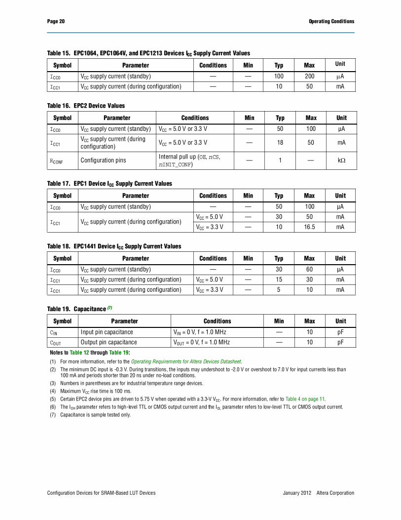
Table 15. EPC1064, EPC1064V, and EPC1213 Devices ICC Supply Current Values
Symbol Parameter Conditions Min Typ Max Unit
ICC0 VCC supply current (standby) — — 100 200 A
ICC1 VCC supply current (during configuration) — — 10 50 mA
Table 16. EPC2 Device Values
Symbol Parameter Conditions Min Typ Max Unit
ICC0 VCC supply current (standby) VCC = 5.0 V or 3.3 V — 50 100 µA
ICC1VCC supply current (during configuration)
VCC = 5.0 V or 3.3 V — 18 50 mA
RCONF Configuration pins Internal pull up (OE, nCS, nINIT_CONF)
— 1 — k
Table 17. EPC1 Device ICC Supply Current Values
Symbol Parameter Conditions Min Typ Max Unit
ICC0 VCC supply current (standby) — — 50 100 µA
ICC1 VCC supply current (during configuration)VCC = 5.0 V — 30 50 mA
VCC = 3.3 V — 10 16.5 mA
Table 18. EPC1441 Device ICC Supply Current Values
Symbol Parameter Conditions Min Typ Max Unit
ICC0 VCC supply current (standby) — — 30 60 µA
ICC1 VCC supply current (during configuration) VCC = 5.0 V — 15 30 mA
ICC1 VCC supply current (during configuration) VCC = 3.3 V — 5 10 mA
Table 19. Capacitance (7)
Symbol Parameter Conditions Min Max Unit
CIN Input pin capacitance VIN = 0 V, f = 1.0 MHz — 10 pF
COUT Output pin capacitance VOUT = 0 V, f = 1.0 MHz — 10 pF
Notes to Table 12 through Table 19:
(1) For more information, refer to the Operating Requirements for Altera Devices Datasheet.(2) The minimum DC input is -0.3 V. During transitions, the inputs may undershoot to -2.0 V or overshoot to 7.0 V for input currents less than
100 mA and periods shorter than 20 ns under no-load conditions.(3) Numbers in parentheses are for industrial temperature range devices.(4) Maximum VCC rise time is 100 ms.(5) Certain EPC2 device pins are driven to 5.75 V when operated with a 3.3-V VCC. For more information, refer to Table 4 on page 11.(6) The IOH parameter refers to high-level TTL or CMOS output current and the IOL parameter refers to low-level TTL or CMOS output current.(7) Capacitance is sample tested only.
Configuration Devices for SRAM-Based LUT Devices January 2012 Altera Corporation

Pin Information Page 21
Pin InformationTable 20 lists the pin functions of the EPC1, EPC2, and EPC1441 devices during device configuration.
f For more information about pin information of EPC devices, refer to the Enhanced Configuration (EPC) Devices Datasheet.
f For more information about pin information of EPCS devices, refer to the Serial Configuration (EPCS) Devices Datasheet.
Table 20. EPC1, EPC2, and EPC1441 Device Pin Functions During Configuration (Part 1 of 3)
Pin Name
Pin Number
Pin Type Description8-PinPDIP (1)
20-PinPLCC
32-PinTQFP (2)
DATA 1 2 31 Output
Serial data output. The DATA pin connects to the DATA0 pinof the FPGA. DATA is latched into the FPGA on the rising edge of DCLK.
The DATA pin is tri-stated before configuration and when the nCS pin is high. After configuration, the EPC2 device drives DATA high, while the EPC1 and EPC1441 device tri-state DATA.
DCLK 2 4 2 Bidirectional
Clock output when configuring with a single configuration device or when the configuration device is the first (master) device in a chain. Clock input for the next (slave) configuration devices in a chain. The DCLK pin connects tothe DCLK pin of the FPGA.
Rising edges on DCLK increment the internal address counter and present the next bit of data on the DATA pin. The counter is incremented only if the OE input is held high, the nCS input is held low, and all configuration data has not been transferred to the target device.
After configuration or when OE is low, the EPC1, EPC2 andEPC1441 device drive DCLK low.
OE 3 8 7 Open-drain bidirectional
Output enable (active high) and reset (active low). The OE pin connects to the nSTATUS pin of the FPGA.
A low logic level resets the address counter. A high logic level enables DATA and the address counter to count. If thispin is low (reset) during configuration, the internal oscillator becomes inactive and DCLK drives low. For moreinformation, refer to “Error Detection Circuitry” on page 9.
The OE pin has an internal programmable 1-k resistor inEPC2 devices. If internal pull-up resistors are used, do notuse external pull-up resistors on these pins. You can disable the internal pull-up resistors through the Disable nCS and OE pull-ups on configuration device option.
Configuration Devices for SRAM-Based LUT DevicesJanuary 2012 Altera Corporation

Page 22 Pin Information
nCS 4 9 10 Input
Chip select input (active low). The nCS pin connects to theCONF_DONE pin of the FPGA.
A low input allows DCLK to increment the address counter and enables DATA to drive out. If the EPC1 or EPC2 deviceis reset (OE pulled low) while nCS is low, the device initializes as the master device in a configuration chain. If the EPC1 or EPC2 device is reset (OE pulled low) while nCSis high, the device initializes as a slave device in the chain.
The nCS pin has an internal programmable 1-k resistor in EPC2 devices. If internal pull-up resistors are used, do not use external pull-up resistors on these pins. You can disable the internal pull-up resistors through the Disable nCS and OE pull-ups on configuration device option.
nCASC 6 12 15 Output
Cascade select output (active low).
This output goes low when the address counter has reached its maximum value. When the address counter hasreached its maximum value, the configuration device has sent all its configuration data to the FPGA. In a chain of EPC1 or EPC2 devices, the nCASC pin of one device is connected to the nCS pin of the next device, which permitsDCLK to clock data from the next EPC1 or EPC2 device in the chain. For single EPC1 or EPC2 device and the last device in the chain, nCASC is left floating.
This pin is only available in EPC1 and EPC2 devices, whichsupport data cascading.
nINIT_CONF N/A 13 16 Open-Drain Output
Allows the INIT_CONF JTAG instruction to initiate configuration. The nINIT_CONF pin connects to the nCONFIG pin of the FPGA.
If multiple EPC2 devices are used to configure an FPGA, the nINIT_CONF of the first EPC2 device pin is tied to the FPGA’s nCONFIG pin, while subsequent devices' nINIT_CONF pins are left floating.
The INIT_CONF pin has an internal 1-k pull-up resistor that is always active in EPC2 devices.
This pin is only available in EPC2 devices.
TDI N/A 11 13 InputJTAG data input pin. Connect this pin to VCC if the JTAG circuitry is not used.
This pin is only available in EPC2 devices.
TDO N/A 1 28 OutputJTAG data output pin. Do not connect this pin if the JTAG circuitry is not used.
This pin is only available in EPC2 devices.
TMS N/A 19 25 InputJTAG mode select pin. Connect this pin to VCC if the JTAG circuitry is not used.
This pin is only available in EPC2 devices.
Table 20. EPC1, EPC2, and EPC1441 Device Pin Functions During Configuration (Part 2 of 3)
Pin Name
Pin Number
Pin Type Description8-PinPDIP (1)
20-PinPLCC
32-PinTQFP (2)
Configuration Devices for SRAM-Based LUT Devices January 2012 Altera Corporation

Pin Information Page 23
TCK N/A 3 32 InputJTAG clock pin. Connect this pin to GND if the JTAG circuitry is not used.
This pin is only available in EPC2 devices.
VCCSEL N/A 5 3 Input
Mode select for VCC supply. VCCSEL must be connected toGND if the device uses a 5.0-V power supply (VCC = 5.0 V).VCCSEL must be connected to VCC if the device uses a 3.3-V power supply (VCC = 3.3 V).
This pin is only available in EPC2 devices.
VPPSEL N/A 14 17 Input
Mode select for VPP. supply. VPPSEL must be connected toGND if VPP uses a 5.0-V power supply (VPP = 5.0 V). VPPSEL must be connected to VCC if VPP uses a 3.3-V power supply (VPP = 3.3 V).
This pin is only available in EPC2 devices.
VPP N/A 18 23 Power
Programming power pin. For the EPC2 device, this pin is normally tied to VCC. If the VCC of the EPC2 device is 3.3 V,tie VPP to 5.0 V to improve ISP time. For EPC1 and EPC1441 devices, VPP must be tied to VCC.
This pin is only available in EPC2 devices.
VCC 7, 8 20 27 Power Power pin.
GND 5 10 12 Ground Ground pin. Place a 0.2-µF decoupling capacitor between the VCC and GND pins.
Notes to Table 20:
(1) This package is available for EPC1 and EPC1441 devices only.(2) This package is available for EPC2 and EPC1441 devices only.
Table 20. EPC1, EPC2, and EPC1441 Device Pin Functions During Configuration (Part 3 of 3)
Pin Name
Pin Number
Pin Type Description8-PinPDIP (1)
20-PinPLCC
32-PinTQFP (2)
Configuration Devices for SRAM-Based LUT DevicesJanuary 2012 Altera Corporation

Page 24 Package
PackageFigure 6 and Figure 7 show the configuration device package pin-outs.
f For more information about package outlines and drawings, refer to the Package and Thermal Resistance page.
Figure 6. EPC1, EPC1064, EPC1064V, EPC1213, and EPC1441 Package Pin-Out Diagrams (1)
Notes to Figure 6:
(1) EPC1 and EPC1441 devices are one-time programmable devices. ISP is not available in these devices. (2) The nCASC pin is available on EPC1 devices, which allows them to be cascaded. For EPC1441 devices, nCASC is a reserved pin and should
be left unconnected.
Figure 7. EPC2 Package Pin-Out Diagrams
8-Pin PDIP 32-Pin TQFP
EPC1441EPC1064EPC1064V
20-Pin PLCC
EPC1EPC1441EPC1213EPC1064EPC1064V
EPC1EPC1441EPC1213EPC1064EPC1064V
DATA
DCLK
OE
nCS
VCC
VCC
nCASC (2)
GND
1
2
3
4
8
7
6
5
1234
5
6
7
8
20 19
10 13
18
17
16
15
14OE
N.C.
N.C.
N.C.
N.C.
N.C.
N.C.
N.C.
DCLK
N.C
.
N.C
.
N.C
.
DA
TA
VC
C
VCC
N.C
.
N.C
.
(2)
nCA
SC
nCS
GN
D
3031321
2
3
4
5
29 28
DCLK
N.C.
N.C.
N.C.
N.C.
N.C.
N.C.
N.C.
N.C.
N.C.
N.C.
N.C.
N.C.N.C.
nCS
GN
D
24
23
22
21
20
VCC
19
18
17
N.C
.N
.C.
N.C
.
N.C
.
N.C
.
N.C
.
N.C
.
N.C
.
N.C
.
N.C
.
N.C
.
N.C
.
DA
TA
VC
C
25
9 168
OE
6
7
10 11 12 13 14 15
27 26
9 11 12
32-Pin TQFP20-Pin PLCC
1234
5
6
7
8
20 19
11109 12 13
18
17
16
15
14OE
N.C.
VCCSEL
DCLK
N.C.
TM
S
TC
K
DAT
A
TD
O
VC
C
VPP
N.C.
N.C.
N.C.
VPPSEL
TD
I
nCA
SC
nCS
GN
D
3031321
2
3
4
5
29 28
N.C.
N.C.
DCLK
N.C.
VCCSEL
TD
I
N.C
.
nCS
N.C
.
GN
D
nIN
IT_C
ON
F
N.C
.
N.C.
24
23
22
21
20
N.C.
VPP
N.C.
N.C.
19
18
17
TD
O
TC
K
DAT
A
N.C
.
N.C
.
TM
S
VC
C
N.C
.
25
9 168N.C.
OE
N.C.
VPPSEL
N.C.
N.C.
6
7
10 11 12 13 14 15
27 26
nCA
SC
nIN
IT_C
ON
F
Configuration Devices for SRAM-Based LUT Devices January 2012 Altera Corporation

Ordering Codes Page 25
Ordering CodesTable 21 lists the ordering codes for the EPC1, EPC2, and EPC1441 configuration devices.
Document Revision HistoryTable 22 lists the revision history for this document.
Table 21. Configuration Device Ordering Codes
Device Package Temperature Ordering Code
EPC1 20-pin PLCC Commercial EPC1LC20
EPC1 20-pin PLCC Industrial EPC1LI20
EPC1 8-pin PDIP Commercial EPC1PC8
EPC1 8-pin PDIP Industrial EPC1PI8
EPC2 32-pin TQFP Commercial EPC2TC32
EPC2 32-pin TQFP Industrial EPC2TI32
EPC2 20-pin PLCC Commercial EPC2LC20
EPC2 20-pin PLCC Industrial EPC2LI20
EPC1441 32-pin TQFP Commercial EPC1441TC32
EPC1441 32-pin TQFP Industrial EPC1441TI32
EPC1441 20-pin PLCC Commercial EPC1441LC20
EPC1441 20-pin PLCC Industrial EPC1441LI20
EPC1441 8-pin PDIP Commercial EPC1441PC8
EPC1441 8-pin PDIP Industrial EPC1441PI8
Table 22. Document Revision History
Date Version Changes
January 2012 3.0 Minor text edits.
December 2009 2.4■ Updated “Features” section.
■ Removed “Referenced Documents” section.
October 2008 2.3
■ Updated “Features” and “IEEE Std. 1149.1 (JTAG) Boundary-Scan Testing” sections.
■ Updated Table 5–2 and Table 5–16.
■ Added “Referenced Documents” section.
■ Updated new document format.
April 2007 2.2 Added document revision history.
July 2004 2.0 Added Stratix II and Cyclone II device information throughout chapter.
September 2003 1.0 Initial Release.
Configuration Devices for SRAM-Based LUT DevicesJanuary 2012 Altera Corporation

Page 26 Document Revision History
Configuration Devices for SRAM-Based LUT Devices January 2012 Altera Corporation


![Vertically Partitioned SRAM-Based Ternary Content ...€¦ · and power consumption [3]. CAM devices have very limited pattern capacity and also the cost of CAM devices is much higher](https://img.dokumen.tips/doc/110x75/6010ad6d6bc305616e2cb423/vertically-partitioned-sram-based-ternary-content-and-power-consumption-3.jpg)