Embed Size (px)
Citation preview

Configurable, High g, iMEMS Accelerometer
Data Sheet ADXL180
Rev. B Document Feedback Information furnished by Analog Devices is believed to be accurate and reliable. However, no responsibility is assumed by Analog Devices for its use, nor for any infringements of patents or other rights of third parties that may result from its use. Specifications subject to change without notice. No license is granted by implication or otherwise under any patent or patent rights of Analog Devices. Trademarks and registered trademarks are the property of their respective owners.
One Technology Way, P.O. Box 9106, Norwood, MA 02062-9106, U.S.A. Tel: 781.329.4700 ©2008–2018 Analog Devices, Inc. All rights reserved. Technical Support www.analog.com
FEATURES Wide sensor range: 50 g to 500 g Adjustable filter bandwidth: 100 Hz to 800 Hz Configurable communication protocol
2-wire, current mode bus interface Selectable sensor data resolution: 8 bit or 10 bit Continuous auto-zero Fully differential sensor and interface circuitry
High resistance to EMI/RFI Sensor self-test 5.0 V to 14.5 V operation 8 bits of user-defined OTP memory 32-bit electronic serial number Dual device per bus option
APPLICATIONS Crash sensing
GENERAL DESCRIPTION The ADXL180 iMEMS® accelerometer is a configurable, single axis, integrated satellite sensor that enables low cost solutions for front and side impact airbag applications. Acceleration data is sent to the control module via a digital 2-wire current loop interface bus. The communication protocol is programmable for compatibility with various automotive interface bus standards.
The sensor g range is configurable to provide full-scale ranges from ±50 g to ±500 g. The sensor signal third-order, low-pass Bessel filter bandwidth is configurable at 100 Hz, 200 Hz, 400 Hz, and 800 Hz.
The 10-bit analog-to-digital converter (ADC) allows either 8-bit or 10-bit acceleration data to be transmitted to the control module. Each part has a unique electronic serial number. The device is rated for operation from −40°C to +125°C and is available in a 5 mm × 5 mm LFCSP package.
FUNCTIONAL BLOCK DIAGRAM
VBN
VDD
ADXL180 VBP
3-POLEBESSELFILTER
TRIMS
10-BIT
ADCVOLTAGE
REGULATOR
COMM INTERFACE
SERIALPORT
STATEMACHINE
SERIALNUMBER
SUPPLYMONITOR
AUTO-ZERO
SYNCDETECT
PROGRAMINTERFACE
CONFIGURATIONDATA
OTPFUSEROM
VBC
SELF-TEST
075
44-0
01
DIFFSENSOR
MOD
OSCILLATOR/TIMING
GENERATOR
DEMODAMP
VCMREF
VSCOVCM
V/QVSCI
Figure 1.

ADXL180 Data Sheet
Rev. B | Page 2 of 60
TABLE OF CONTENTS Features .............................................................................................. 1 Applications ....................................................................................... 1 General Description ......................................................................... 1 Functional Block Diagram .............................................................. 1 Revision History ............................................................................... 3 Specifications ..................................................................................... 4 Absolute Maximum Ratings ............................................................ 7
ESD Caution .................................................................................. 7 Pin Configuration and Function Descriptions ............................. 8 Terminology ...................................................................................... 9 Theory of Operation ...................................................................... 10
Overview ...................................................................................... 10 Acceleration Sensor .................................................................... 10 Signal Processing ........................................................................ 11 Digital Communications State Machine ................................. 11 2-Wire Current Modulated Interface ....................................... 11 Synchronous Operation and Dual Device Bus ....................... 11 Programmed Memory and Configurability ............................ 11
Physical Interface ............................................................................ 13 Application Circuit ..................................................................... 13 Current Modulation ................................................................... 13 Manchester Data Encoding ....................................................... 14 Operation at Low VBP or Low VDD............................................ 14 Operation at High VDD ............................................................... 14
Communications Timing and Bus Topologies ........................... 15 Data Transmission ...................................................................... 15 Asynchronous Communication ............................................... 16 Synchronous Communication .................................................. 17 Synchronous Communication Mode—Dual Device ............. 19
Data Frame Definition ................................................................... 23 Data Frame Transmission Format ............................................ 23 Data Frame Configuration Options ......................................... 23 Acceleration Data Coding ......................................................... 25 State Vector Coding ................................................................... 26 State Vector Descriptions .......................................................... 26 Transmission Error Detection Options ................................... 27
Application Layer: Communication Protocol State Machine ... 28 ADXL180 State Machine ........................................................... 28 Phase 1: Power-on-Reset Initialization .................................... 28 Phase 2: Device Data Transmission ......................................... 28
Phase 2: Mode Description ....................................................... 30 Phase 3: Self-Test Diagnostic .................................................... 37 Phase 4: Auto-Zero Initialization ............................................. 40 Phase 5: Normal Operation ...................................................... 40
Signal Range and Filtering ............................................................ 41 Transfer Function Overview ..................................................... 41 Range ............................................................................................ 41 Three-Pole Bessel Filter ............................................................. 41 Auto-Zero Operation ................................................................. 41
Error Detection ............................................................................... 43 Overview ..................................................................................... 43 Parity Error Due to Communications Protocol Configuration Bit Error ....................................................................................... 43 Self-Test Error ............................................................................. 44 Offset Error/Offset Drift Monitoring ...................................... 44 Voltage Regulator Monitor Reset Operation .......................... 44
Test and Diagnostic Tools.............................................................. 45 VSCI Signal Chain Input Test Pin .............................................. 45 VSCO Analog Signal Chain Output Test Pin ............................ 45
Configuration Specification .......................................................... 46 Overview ..................................................................................... 46 Configuration Mode Transmit Communications Protocol .. 47 Configuration Mode Command (Receive) Communications Protocol........................................................................................ 48 Configuration Mode Communications Handshaking .......... 49 Configuration and User Data Registers .................................. 50 Configuration Mode Exit .......................................................... 50 Serial Number and Manufacturer Identification Data Registers ....................................................................................... 50 Programming the Configuration and User Data Registers .. 50 OTP Programming Conditions and Considerations ............ 51 Configuration/User Register OTP Parity ................................ 51 Configuration Mode Error Reporting ..................................... 51
Configuration Register Reference ................................................ 52 UD[7:0] User Data Bits .............................................................. 53 UD8 Configuration Bit .............................................................. 53 BDE .............................................................................................. 53 SCOE ............................................................................................ 53 FDLY ............................................................................................ 53 ADME .......................................................................................... 53 STI ................................................................................................ 53

Data Sheet ADXL180
Rev. B | Page 3 of 60
FC[1:0] .......................................................................................... 53 RG[2:0] ......................................................................................... 53 MD[1:0] ........................................................................................ 54 SYEN ............................................................................................. 55 AZE ............................................................................................... 55 ERC ............................................................................................... 55 DAT ............................................................................................... 55
SVD ............................................................................................... 55 CUPAR and CUPRG .................................................................. 55
Axis of Sensitivity ............................................................................ 56 Branding ........................................................................................... 57 Outline Dimensions ........................................................................ 58
Ordering Guide ........................................................................... 58
REVISION HISTORY 1/2018—Rev. A to Rev. B Updated Outline Dimensions ........................................................ 28 Change to Ordering Guide ............................................................ 58
11/2008—Rev. 0 to Rev. A Added Data Transmission Section ................................................ 15 Added New Figure 10, Renumbered Sequentially ...................... 15 Added New Figure 11 ..................................................................... 16 Changes to Figure 14 ...................................................................... 18 Changes to Figure 16 ...................................................................... 20 Changes to Synchronization Pulse Detection Section ............... 17
8/2008—Revision 0: Initial Version

ADXL180 Data Sheet
Rev. B | Page 4 of 60
SPECIFICATIONS TA = −40°C to +125°C, VBP − VBN = 5.0 V to 14.5 V, fLP = 400 Hz, acceleration = 0 g, unless otherwise noted.
Table 1. Parameter1 Symbol Min Typ Max Unit Test Conditions/Comments SENSOR
Scale Factor Measurement frequency: 100 Hz 50 g Range See Table 37
8-Bit Data 0.465 0.50 0.535 g/LSB 10-Bit Data 0.116 0.1250 0.134 g/LSB
100 g Range 8-Bit Data 0.930 1.00 1.070 g/LSB 10-Bit Data 0.233 0.2500 0.268 g/LSB
150 g Range 8-Bit Data 1.395 1.50 1.605 g/LSB 10-Bit Data 0.349 0.3750 0.401 g/LSB
200 g Range 8-Bit Data 1.860 2.00 2.140 g/LSB 10-Bit Data 0.465 0.5000 0.535 g/LSB
250 g Range 8-Bit Data 2.325 2.50 2.675 g/LSB 10-Bit Data 0.581 0.625 0.669 g/LSB
350 g Range 8-bit Data 3.255 3.50 3.745 g/LSB 10-bit Data 0.830 0.8925 0.955 g/LSB
500 g Range 8-Bit Data 4.650 5.00 5.350 g/LSB 10-Bit Data 1.163 1.2500 1.338 g/LSB
Offset All ranges, auto-zero disabled 8-Bit Data −12 +11 LSB 10-Bit Data −48 +47 LSB
Noise (Peak-to-Peak) 50 g range 8-Bit Data 2 LSB 10 Hz to 400 Hz 10-Bit Data 2 3 LSB 10 Hz to 400 Hz
Self Test Amplitude 20 25 30 g Internal Self-Test Limit 20 30 g STI enabled, see Table 35
Nonlinearity 0.2 2 % Of full-scale range Cross-Axis Sensitivity −5 +5 % Resonant Frequency 12.8 kHz Q 1.5
LOW-PASS FILTER Frequency Response Third-order
Bessel
Pass Band fLP Programmable, see Table 38 −3 dB Frequency 670 800 880 Hz −3 dB Frequency 335 400 440 Hz −3 dB Frequency 167.5 200 220 Hz −3 dB Frequency 83.75 100 110 Hz
AUTO-ZERO Update Rate
Slow Mode 5.0 sec/LSB 10-bit LSB Fast Mode 0.5 sec/LSB 10-bit LSB

Data Sheet ADXL180
Rev. B | Page 5 of 60
Parameter1 Symbol Min Typ Max Unit Test Conditions/Comments REGULATOR VOLTAGE MONITOR
Regulator Operating Voltage VDD 4.20 V Power-Up Reset Voltage VPUR 3.77 4.0 4.23 V See Figure 33 Overvoltage Level VOV 4.7 4.95 5.3 V See Figure 33 Reset Hysteresis Voltage VHYST 0.12 V
COMMUNICATIONS INTERFACE Quiescent (Idle) Current ILDLE 5 6 7.7 mA Modulation Current IMOD 23 25 30 mA Signal Current ISIG 28 31 37.7 mA ISIG = IIDLE + IMOD Autodelay Detect Current IDET 18 22 26 mA Total including IIDLE Data Bit Period2 tB 8 μs tB = 8 × tCLK Data Bit Duty Cycle DDC 45 50 53 % DDC = tA/tB, see Figure 7 Data Bit Rise/Fall See Figure 7
Fall Time tR 400 1000 ns Rise Time tF 350 1000 ns
Encoding Manchester See Figure 8 ADC Conversion Time2 tADC 35 μs See Figure 12 Error Checking (Selectable) Number of CRC Bits 3 x³ + x¹+ x0 Number of Parity Bits 1 Even Synchronization Pulse Detect
No Detect Limit VSPND 3.0 V Detect Threshold VSPT 3.5 V VBP − VBN + VSPT ≤ 14.5 V; see Figure 14
Threshold Hysteresis 0.1 V Synchronization Pulse Detect
Time tSPD 8 tCLK See Figure 14
Synchronization Pulse Discharge (Pull-Down) Time
tSPP 40 tCLK See Figure 14
Synchronization Mode Transmission Delay
tSTD 63 tCLK See Figure 14
Configuration Mode Receive Communications Interface
All @ 25°C only; VBP − VBN + VCT ≤ 12.25 V
Detect Threshold VCT 5.25 V See Figure 35 Threshold Hysteresis 0.1 V Interbit Time tIB 250 tCLK See Figure 35 Data 0 Pulse Width tPG0 40 55 tCLK See Figure 35 Data 1 Pulse Width tPG1 80 tCLK See Figure 35 Configuration Mode
Response Time tTM1 24 μs See Figure 35
Configuration Mode Write Delay Time
tTM2 50 μs See Figure 35
VBP During Fuse Programming
VBPF 7.5 V Compliant up to the maximum operating voltage
VBP Current During Fuse Programming
IFP 15 mA Maximum drawn by the part

ADXL180 Data Sheet
Rev. B | Page 6 of 60
Parameter1 Symbol Min Typ Max Unit Test Conditions/Comments ASYNCHRONOUS MODE TIMING2
Message Transmission Period Phase 2, Mode 0 tPM0 456 μs ADIFX compatible All Other Phases and Modes tP 228 μs
Initialization State (Phase 1) tI 100 ms Device Data State (Phase 2) ms
Mode 0 tDD0 4.10 ms Mode 1 tDD1 109 ms Mode 2 tDD2 109 ms Mode 3 tDD3 117 ms
Self-Test State (Phase 3) Self-Test Time3 tST 394 ms See Figure 28 Self-Test Interval tSTI 21.9 ms See Figure 28 Self-Test Cycle tSTC 65.7 ms See Figure 28
Auto-Zero Initialization State (Phase 4)
tAZ 14.94 sec
SYNCHRONOUS MODE TIMING4 Message Transmission Period tPS N/A Determined by sync pulse, See Figure 14,
minimum tPS = tSPD + tSTD + tM + tB Initialization State1 (Phase 1) tI 100 ms Device Data State (Phase 2) ms
Mode 0 tDD0s 9 × tPS ms Mode 1 tDD1s 480 × tPS ms Mode 2 tDD2s 480 × tPS ms Mode 3 tDD3s 512 × tPS ms
Self-Test State (Phase 3) Self-Test Time3 tSTS 1728 × tPS ms Self-Test Interval tSTIS 96 × tPS ms Self-Test Cycle tSTCS 288 × tPS ms Auto-Zero Initialization State
(Phase 4) tAZs 65,535 × tPS sec
CLOCK Period2 tCLK 1.05 1.0 0.95 μs fCLK = 1/tCLK
PSRR <1 LSB 8-bit LSB; test conditions: VBP − VBN = 7.00 V, VAC = 500 mV p-p, 100 kHz to 1.1 MHz
POWER SUPPLY HOLDUP TIME 500 ns @ IBUS = ISIG THERMAL RESISTANCE, JUNCTION
TO CASE θJC 30 °C/W
1 All parameters are specified using the application circuit shown in Figure 6. CB = 10 nF, CVDD = 100 nF. 2 All timing is driven from the on-chip master clock. 3 tST and tSTS are the times for six self-test cycles. This is the maximum number of cycles in the internal self-test mode. 4 Transmission timing is defined by the internal system clock in asynchronous mode and by the synchronization pulse period in synchronous mode.

Data Sheet ADXL180
Rev. B | Page 7 of 60
ABSOLUTE MAXIMUM RATINGS Table 2. Parameter Rating Supply Voltage (VBP − VBN) −0.3 V to +21 V Voltage at Any Pin with
Respect to VBN Except VBP −0.3 V to VDD + 0.3 V
Storage Temperature Range −55°C to +150°C Soldering Temperature 255°C Operating Temperature Range −40°C to +125°C ESD All Pins 1.5 kV HBM Latch-Up Current 100 mA Mechanical Shock
Unpowered ±4000 g (0.5 ms, half sine) Powered ±2000 g (0.5 ms, half sine);
−0.3 V to +7.0 V Drop Test (onto Concrete)1 1.2 m Thermal Gradient ±20°C/minute 1 Soldered to FR4 coupon printed circuit board (PCB) at the dimensions of
25.4 mm × 25 mm. During test, the PCB is fastened to a support with 46 g mass, equivalent to a typical satellite module PCB.
Stresses at or above those listed under Absolute Maximum Ratings may cause permanent damage to the product. This is a stress rating only; functional operation of the product at these or any other conditions above those indicated in the operational section of this specification is not implied. Operation beyond the maximum operating conditions for extended periods may affect product reliability.
ESD CAUTION
RAMP-DOWN
RAMP-UP
CRITICAL ZONEtL TO tP
TEM
PER
ATU
RE
TA = 25°C
tL
tP
TIMEt = 25°C TO PEAK
tSPREHEAT
tL
tP
TSMIN
TSMAX
0754
4-00
2
Figure 2. ADXL180 Pb-Free Solder Profile
Table 3. ADXL Solder Profile Parameters Profile Feature Small Body Pb-Free Assemblies Average Ramp-Up Rate (TL to TP) 3°C/second maximum Preheat Temperature Min (TS min) to Temperature Max (TS max) 150°C to 200°C
Time (min to max) (tS) 60 sec to 180 sec TS max to TL Ramp-Up Rate 3°C/second maximum Time Maintained Above Temperature (TL) 217°C
Time (tL) 60 sec to 150 sec Peak Temperature (TP) 260°C +5/−5°C Time Within 5°C of Actual Peak Temperature (tP) 20 sec to 40 sec Ramp-Down Rate 6°C/sec maximum Time 25°C to Peak Temperature 8 minutes maximum

ADXL180 Data Sheet
Rev. B | Page 8 of 60
PIN CONFIGURATION AND FUNCTION DESCRIPTIONS
VDD NC VSCO
VCMVCM
VBP
VBN
VBCNC
NC
NC
9
10
11
12
VBN
VCM
13141516
VCM NCVSCI
4
3
2
1
876
VBN
5
VBN
NC = NO CONNECT
DAP1
ADXL180TOP VIEW
(Not to Scale)
DAP2
0754
4-00
3
Figure 3. Pin Configuration
Table 4. Pin Function Descriptions Pin No. Mnemonic Description 1 NC Reserved for Analog Devices, Inc., Use Only. VBN or do not connect. 2 VCM Reserved for Analog Devices Use Only. Do not connect. 3 VBN Negative Bus Voltage. 4 NC Reserved for Analog Devices Use Only. VBN or do not connect. 5 VDD Voltage Regulator Bypass Capacitor. 6 NC Reserved for Analog Devices Use Only. VBN or do not connect. 7 VSCO Reserved for Analog Devices Use Only. Do not connect. 8 VBN Negative Bus Voltage. 9 VBC Daisy-Chain Connection. Daisy-chain connection to VBP of the second device or do not connect. 10 VBN Negative Bus Voltage. 11 VCM Reserved for Analog Devices Use Only. Do not connect. 12 VBP Positive Bus Voltage. 13 NC Reserved for Analog Devices Use Only. VBN or do not connect. 14 NC Reserved for Analog Devices Use Only. VBN or no connect 15 VSCI Analog Signal Chain Input. VBN when not in use. 16 VCM Reserved for Analog Devices Use Only. Do not connect. DAP1 VCM Exposed Pad: Reserved for Analog Devices Use Only. Do not connect. DAP2 VBN Exposed Pad: Negative Bus Voltage.

Data Sheet ADXL180
Rev. B | Page 9 of 60
TERMINOLOGY Full-Scale Range (FSR)
The full-scale range of a device, also referred to as the dynamic range, is the maximum and minimum g level that reports on the output following the internal filtering. As a reference, there is usually a trade-off in increased sensitivity and resolution for decreased full-scale range, and vice versa.
Noise Device noise is the noise content between 10 Hz and 400 Hz, as noted in the Specifications Table 1. Device noise can be measured by performing an FFT on the digital output and measuring the noise content between the specified frequency limits.
Sensitivity The sensitivity of a device is the amount of output change per input change. In this device, it is most usually referred to in units of LSB/g.
Scale Factor
The scale factor is the amount of input change per output change. In this device, it is most usually referred to in units of g/LSB.
Offset Offset is the low frequency component of the output signal that is not due to changes in input acceleration. Slow moving effects, such as temperature changes and self-heating during start up, may affect offset, but the time scale for these effects is beyond that of a typical shock or crash event.
Auto-Zero Auto-zero is an offset compensation technique intended to reduce the long term offset drift effects of temperature and aging. This technique is designed to limit interaction with true acceleration signals. For more information, see Figure 32.
Rise/Fall Times The device rise time is defined as the amount of time necessary for the Manchester encoded signal (IMOD) to transition from 10% to 90% of its final value (ISIG). Device fall time is the amount of time required for the IMOD signal to fall from 90% of ISIG to within 10% of IIDLE.
Idle Current Idle current is the current of the device when at rest, waiting for a synchronization pulse, or in between current modulation.
Modulation Current Modulation current is the amount of current that the ADXL180 device pulls from the bus when communicating. For more information, see Figure 7.
Phase A phase is a stage in the ADXL180 state machine. For more information, see Figure 22.
Mode Mode refers to the selection of the Phase 2 method of device data communication. The ADXL180 is configurable into four unique operating modes.
CRC A cyclic redundancy check (CRC) is calculated from a set of data and then transmitted alongside that data. If the calculation technique is defined and known to the receiving device, the receiver can then check whether the CRC bits match the data. If they do not match, a transmission error has occurred.
Parity Parity is defined by the count of 1s in a binary string of data. If this count is even, then the data is determined to have even parity. Often a bit is used, such as the CUPAR, in a configuration register that is defined in such a way as to establish a particular parity in the register to detect single bit changes during the life of the device. This is possible because a single bit change changes parity and a monitor circuit can detect this. Similarly, a parity bit can be added in a data transmission to detect single bit errors if the parity of communication is preestablished for the transmit and receive systems.

ADXL180 Data Sheet
Rev. B | Page 10 of 60
THEORY OF OPERATION OVERVIEW The ADXL180 is a complete satellite system, including acceleration sensor, data filtering, digital protocol functionality, and a 2-wire, high-voltage, current-modulated bus interface communications port.
ACCELERATION SENSOR The ADXL180 provides a fully differential sensor structure and circuit path. This device uses electrical feedback with zero force feedback. Figure 4 is a simplified view of one of the differential sensor elements. Each sensor includes several differential capa-citor unit cells. Each cell is composed of fixed plates attached to the substrate and movable plates attached to the frame. Displacement of the frame changes the differential capacitance, which the on-chip circuitry measures.
Complementary signals drive the fixed capacitor plates. The relative phasing between the two halves of the differential
sensor is such that the displacement signal is differential between the two measurement channels. Using the fully differential sensor and an antiphase clocking scheme helps reject electrical environmental noise (see Figure 5).
The ADXL180 acceleration sensor uses two electrically isolated, mechanically coupled sensors to measure acceleration as shown in Figure 5. The clock phasing of the readout is such that the electrical signal due to acceleration is differential between the channels and environmental disturbances couple in as a common-mode signal. The following differential amplifier can then extract the acceleration signal while suppressing the environmental noise.
Electrical feedback adjusts the amplitudes of the fixed capacitor plates’ drive signals such that the ac signal on the moving plates is zero. The feedback signal is linearly proportional to the applied acceleration. This feedback technique ensures that there is no net electrostatic force applied to the sensor.
MOVABLEFRAME
A
CC
ELER
ATI
ON
UNIT SELF-TESTFORCING CELL
UNIT SENSINGCELL
MOVINGPLATE
FIXEDPLATES
PLATECAPACITORS
ANCHOR
ANCHOR
M
OTI
ON
0754
4-00
4
Figure 4. Simplified View of ADXL180 Sensor Under Acceleration
AMP
–
VOUT
0
+
–
EMI DISTURBANCE RESPONSECOMMON TO BOTH CHANNELS
ACCELERATION RESPONSEDIFFERENTIAL BETWEEN CHANNELS
0
ACCELERATION SENSING AXIS
+X-AXIS SENSOR
–X-AXIS SENSOR
ISOLATEDMECHANICALCOUPLINGS
+
SPRING
0754
4-00
5
Figure 5. Differential Acceleration Sensing

Data Sheet ADXL180
Rev. B | Page 11 of 60
SIGNAL PROCESSING The ADXL180 contains an on-board set of signal processing blocks both prior to and after ADC conversion. The first stage is a fully differential, switched capacitor, low-pass, three-pole Bessel filter. Range scaling is also handled in one of the filter blocks, enabling 50 g to 500 g range capability. At this point, an analog output test signal (VSCO) is available to the user in a diagnostic mode. The signal then converts by a 10-bit rail-to-rail SAR ADC. In the digital section, an auto-zero routine is available to the user as part of the state machine in addition to error detection features such as offset drift detection.
DIGITAL COMMUNICATIONS STATE MACHINE The ADXL180 digital state machine is based on a Core 5 phase state machine implemented in high density CMOS. This state machine handles the sequential states of
Phase 1. Initialization. Phase 2. Device data transmission, including individual serial
number and user-programmed data. Phase 3. Self-diagnostic, including automatic full electro-
mechanical self-test with internal error detection available.
Phase 4. Auto-zero initialization, if selected. During this phase, acceleration data is already available.
Phase 5. Normal acceleration data transmission.
2-WIRE CURRENT MODULATED INTERFACE The data that is generated during these five phases is trans-mitted using a 2-wire high voltage communication port. This allows the device to be powered by a fixed supply voltage, and communicate back to the system or ECU electronics by modulating current. Current modulated messages are encoded using Man-chester encoding.
SYNCHRONOUS OPERATION AND DUAL DEVICE BUS In a point-to-point bus topology, the ADXL180 supports asyn-chronous transmission of data to the receive device every 228 μs, controlled by the on-board state machine. A synchronous option is also available, allowing two devices to be on the same bus using time division multiplexing where each device transmits its data during a known time slot.
Synchronization is achieved by voltage modulated synchronization pulses, configuring the ADXL180 device into a synchronous mode, and establishing data frame time slots. The high voltage communication port registers valid synchronization pulses and enables message-by-message advancement of the state machine rather than asynchronous timed regular data transmission.
PROGRAMMED MEMORY AND CONFIGURABILITY Factory-Programmed Serial Number and Manufacturer Information
The ADXL180 includes a 32-bit factory-programmed serial number, as shown in Table 5. This serial number transmits during Phase 2 of startup for all devices to enable robust quality tracking of individual devices, and it is field readable. In addition, this data includes revision information and manufacturer identi-fication in case multiple devices used within a single application are from different manufacturers or generations of parts.
User-Programmable Data Register
The ADXL180 gives the user an 8-bit register of user-program-mable data, which is transmitted during Phase 2 of the state machine. In addition, the UD8 bit, a ninth user-available bit, is transmitted separately during Phase 2 and can be used for various purposes, such as orientation definition or module type.
Table 5. Factory Programmed and User-Programmed Memory
Programmed By Configuration Mode Register Address
Configuration Mode Register Name
MSB D6 D5 D4 D3 D2 D1
LSB D7 D0
User 0000b UREG UD7 UD6 UD5 UD4 UD3 UD2 UD1 UD0 0001b CREG0 UD8 BDE MD1 MD0 FDLY DLY2 DLY1 DLY0 0010b CREG1 STI AZE SYEN ADME ERC SVD DAT MAN 0011b CREG2 CUPRG CUPAR SCOE FC1 FC0 RG2 RG1 RG0
Factory 1011b SN0 SNB7 SNB6 SNB5 SNB4 SNB3 SNB2 SNB1 SNB0 1100b SN1 SNB15 SNB14 SNB13 SNB12 SNB11 SNB10 SNB9 SNB8 1101b SN2 SNB23 SNB22 SNB21 SNB20 SNB19 SNB18 SNB17 SNB16 1110b SN3 SNB31 SNB30 SNB29 SNB28 SNB27 SNB26 SNB25 SNB24 1111b MFGID SNPRG SNPAR REV2 REV1 REV0 MFGID2 MFGID1 MFGID0

ADXL180 Data Sheet
Rev. B | Page 12 of 60
User-Programmed Configuration
At each of these previously described points in the system, the ADXL180 is highly configurable for different applications. The organization and configurable items are briefly described in this section but are covered in depth in the remainder of this data sheet.
Physical Layer (ISO Layer 1)
The bus interface hardware definition including the phase of Manchester encoding and synchronization pulse enable/disable.
Data Link Layer (ISO Layer 2)
The specifics of the data frame format including the data width (8-bit or 10-bit data), state vector (enable/disable), and error detection (parity or CRC).
Application Layer (ISO Layer 7)
The serial number and configuration data transmission mode and self-test (internal self-test pass/fail discrimination or external self-test data evaluation).
Other signal processing related aspects of the function of the ADXL180 can also be configured as follows:
• Sensor scale factor (range) • Signal chain low-pass filter bandwidth • Auto-zero: enable/disable • User-defined data in the user data register

Data Sheet ADXL180
Rev. B | Page 13 of 60
PHYSICAL INTERFACE APPLICATION CIRCUIT A typical application circuit is shown in Figure 6. The two capa-citors shown in Figure 6 are typically ceramic, X7R, multilayer SMT capacitors. Maximum recommended values of ESR and ESL are 250 mΩ and 2 nH, respectively. Capacitor tolerances of ±10% are recommended.
CURRENT MODULATION When the ADXL180 device is powered on, it uses current modulation to transmit data. Normally, the device pulls IIDLE current. When modulating, an additional current of IMOD is pulled from the sensor bus. See Figure 7.
ADXL180
VBP
VDD
VBN
VBP
SUPPLY ANDCONFIGURATION
BUS
VBN
CVDD100nF
CB10nF
075
44-0
06
Figure 6. Application Circuit
IIDLE
tB
IMOD
TIME
tA
10%
50%
90%
tRF
0754
4-0
07
Figure 7. Communication Current Modulation Timing

ADXL180 Data Sheet
Rev. B | Page 14 of 60
MANCHESTER DATA ENCODING To encode data within the current modulation, the ADXL180 uses Manchester encoding. Manchester encoding works on the principle of transitions representing binary 1s and 0s, as shown in Figure 8. Manchester encoding uses a set of predefined start bits to transmit the clocking within each message, see Figure 9. The pattern of the start bits allows the receiver to synchronize itself to the bit stream. These start bits are user selectable.
LOGIC 0 LOGIC 1
START BITS
ISIG
IIDLE
LOGIC 0LOGIC 1
BUSCURRENT
0754
4-00
8
Figure 8. Manchester-1, Start Bits and Phase
LOGIC 0 LOGIC 1
START BITS
ISIG
IIDLE
LOGIC 0LOGIC 0
0754
4-00
9
BUSCURRENT
Figure 9. Manchester-2, Bit Coding
Table 6. MAN Options
MAN Manchester Coding
Start Bits Logic 0 Logic 1
0 Manchester-1 (Default)
1, 0 Falling edge Rising edge
1 Manchester-2 0, 0 Rising edge Falling edge
The phase of the Manchester encoded data can be selected via a bit in the configuration registers. See Figure 8 and Figure 9 for details. The configuration bit that sets the phase of the Man-chester encoder also sets the value of the two start bits. The start bits are 1, 0 for Manchester-1 and 0, 0 for Manchester-2. For phase and start bit information, see Table 6.
OPERATION AT LOW VBP OR LOW VDD The ADXL180 monitors its internal regulator voltage to ensure proper operation. If the bus voltage drops, or the internal regu-lator voltage drops below the VPUR reset threshold, the device resets. See the Voltage Regulator Monitor Reset Operation section.
OPERATION AT HIGH VDD If the regulator pin detects a high voltage, such as from a short or leakage condition, the ADXL180 detects an error. See the Voltage Regulator Monitor Reset Operation section for more details.

Data Sheet ADXL180
Rev. B | Page 15 of 60
COMMUNICATIONS TIMING AND BUS TOPOLOGIES DATA TRANSMISSION The analog data (available to the user by enabling the VSCO output) is sampled every 228 μs when the device is configured to run asynchronously. In synchronous operation, an ADC conversion is triggered upon the detection of a valid sync pulse. In both cases, the data is held until a subsequent ADC conversion is performed. This results in an additional time delay of either 228 μs or one sync pulse period from the
sampling of the analog data to when it is transmitted via manchester encoded data. Analog-to-digital conversions are performed prior to the device entering run-time mode (Phase 5) thereby ensuring that the data from the ADC is never in an unknown state. This holds true upon receipt of the first sync pulse in run-time mode (Phase 5).
INPUTACCELERATION
ADC CONVERSION(38µs CONVERSION
EVERY 228µs.)
ADXL180 RETURNCURRENT
DIGITALWAVEFORM
THE DATA ACQUIRED DURING A GIVEN ADC CYCLE IS NOTTRANSMITTED UNTIL A SUBSEQUENT DATA ACQUISITIONIS PERFORMED. IN ASYNCHRONOUS OPERATION MODE,THIS DELAY 228µs.
n–2 n–1
n–3 n–2 n–1
n0
n0
n1
n1
n2
n3
n4 n5
n6n7
n8n9
n0n1
n2
n3n4 n5
n6n7
n8
075
44-0
10
…
…
…
…
… Figure 10. Asynchronous Data Transmission (Timing Not To Scale)

ADXL180 Data Sheet
Rev. B | Page 16 of 60
INPUTACCELERATION
ADC CONVERSION(PERFORMED AFTER SYNC
PULSE DETECTION)
SYNC PULSE
ADXL180 RETURNCURRENT
DIGITALWAVEFORM
n–2 n–1
n–3 n–2 n–1
n0
n0
n0
n1
n2
n3
n4 n5
n6n7
n8n9
n0n1
n2
n3n4 n5
n6n7
n8
075
44-0
11
ONCE A VALID SYNC PULSE IS DETECTEDTHE DEVICE WILL PERFORM AN ADCCONVERSION ON THE (AVAILABLE) ANALOGINPUT SIGNAL.
THE DATA FROM THE ADC CONVERSIONIS HELD UNTIL A SUBSEQUENT SYNC PULSEIS TRANSMITTED TO THE DEVICE.
…
…
…
…
…
Figure 11. Synchronous Data Transmission (Timing Not To Scale)
ASYNCHRONOUS COMMUNICATION
LOOP CURRENT
IIDLE
IMOD
tM2 tM
2
TIME
ADC SAMPLE tADC
tP1
0754
4-0
12
tP1
1tP = tDD DURING PHASE 2, MODE 02tM = tCLK TIMES THE NUMBER OF BITS TRANSMITTED
DATA FRAME DATA FRAME
Figure 12. Asynchronous Mode Data Transmission Timing
The ADXL180 data transmissions in their default mode run asynchronous to the control module. In this mode, the ADXL180 timing is entirely based on the internal clock of the device. After the initialization phases are complete, the ADXL180 begins to transmit sensor data every 228 μs. The device transmits sensor data until the supply voltage falls below the required minimum operating level. If an internal error is detected, the device trans-mits the appropriate error code until the supply voltage falls below the required minimum operating level.
Asynchronous Single Device Point-to-Point Topology
A single device is wired in the point-to-point configuration as shown in Figure 13. This configuration must be used in asynchronous mode. Do not use two asynchronous devices on one bus because communications errors are very likely to occur.

Data Sheet ADXL180
Rev. B | Page 17 of 60
CENTERMODULE
VBP
DEVICE 1
NC NC
VBN VBN VBC
0754
4-0
13
Figure 13. Asynchronous Point-To-Point Topology
SYNCHRONOUS COMMUNICATION The ADXL180 data transmission can be synchronized to the control module. This synchronization is accomplished by the control module generating a synchronization pulse to the ADXL180. The synchronization pulse is a voltage pulse that is superimposed on the supply voltage by the center module. Figure 14 shows the synchronization pulse timing. Upon detecting a synchronization pulse, the ADXL180 transmits its data.
Configuring the ADXL180 for Synchronous Operation
Table 7. Sync Enable (SYEN) Options SYEN Definition 0 Synchronization pulse disabled. The device transmits
data every 228 μs based on the internal clock of the device. Data is transmitted according to an internal state machine sequence when powered on (default).
1 Synchronization pulse enabled. The device requires a synchronization pulse to sample and transmit data. Data transmission is in accordance with the internal state machine of the device.
The user-defined SYEN bit determines whether the device is used in synchronous operation or remains asynchronous. SYEN, as shown in Table 7, must be set to SYEN = 1 to enable synchronous operation.
Synchronization Pulse Detection
The ADXL180 uses a digital integration method to validate the synchronization pulse. The ADXL180 detects the supply voltage (VBP) rising above the level of VSPT. The state of the level detection circuit controls the count direction of an up-down counter. The counter is clocked every 1 μs. The counter is incremented if the ADXL180 detects a level exceeding VSPT. The counter is decre-mented if the ADXL180 detects a level below VSPND. Operation is not defined between these thresholds. If the synchronization
pulse is fully below VSPND, the pulse is rejected and not detected. The counter saturates at zero. The synchronization pulse is con-sidered valid on the next clock after the counter is incremented to seven counts. The counter is gated off (blanked) after a valid synchronization pulse is detected. Once the sync pulse has been recognized as valid, a command is issued to start the acceleration data analog-to-digital conversion. The ADC does not run conti-nuously in synchronous mode.
The synchronization pulse detector is reenabled after tB, which is an idle bit transmission following the last data frame bit (see the Data Frame Definition section). At this point, the device is ready to receive the next sync pulse.
If the application requires or uses a pulse of nonuniform shape, such as, for example, rising above VSPT and subsequently toggling such that it falls below VSPT one or more times before tSPD, consult Analog Devices, Inc., applications support for further information on application specific pulse recognition.
Note, this counter means that when an invalid length sync pulse of less than seven counts is followed less than seven counts later by a subsequent sync pulse, detection may occur when the counter is incremented further by less than seven counts by the second pulse.
Bus Discharge Enable
Table 8. Bus Discharge Enable BDE Definition 0 Bus discharge disabled (default). 1 Bus discharge enabled. Only active when SYEN = 1.
The bus discharge enable (BDE) bit in the configuration registers can be set to aid in the discharge of the bus voltage after a syn-chronization pulse is detected. If the BDE bit is set, the ADXL180 changes the bus current (IBUS) level from IIDLE to ISIG once a valid synchronization pulse is detected. The control module then sets the voltage on the bus to the nominal operating level. The bus capacitance is discharged by the ADXL180 device. The current level of ISIG acts as an active pull-down current to return the VBP voltage to the nominal supply voltage. The pull-down current pulse can also be used as a handshake with the control module acting as an acknowledgement of the synchronization pulse.

ADXL180 Data Sheet
Rev. B | Page 18 of 60
VSP
VSPND
VSPT
tADC
tADC
tPS
tSPDtB
tSPD
tSPP
tSTD
tM
0754
4-01
4
BUSVOLTAGE
NO DETECT CASE DETECT CASE
SYNC DETECT BLANKING
DATA FRAME DATA FRAME
SYNCHDETECT/
BLANKING
ADC BUSY
BUS DISCHARGE CURRENT(IF BDE = 1)
ADXL180RETURN
CURRENT
BUS DISCHARGECURRENT
(IF BDE = 1)
DATA CONTAINED IS FROMTHE PERVIOUS ADC CONVERSION.
Figure 14. Synchronization Pulse Timing (Single Device)

Data Sheet ADXL180
Rev. B | Page 19 of 60
Synchronous Single Device Point-to-Point Topology
A single device is wired in the point-to-point configuration as shown in Figure 15. The standard use of this configuration is with no delay devices. It is possible to use this topology with fixed delay devices as well, such as if line noise reduction after a sync pulse transmission is desired.
CENTERMODULE
VBP
DEVICE 1
NC NC
VBN VBN VBC
0754
4-01
5
Figure 15. Single Device—Synchronous Communication
SYNCHRONOUS COMMUNICATION MODE—DUAL DEVICE The ADXL180 can be used in a dual device synchronous communication mode. This mode allows a maximum of two
ADXL180 devices to share a single pair of wires from the control module for power and communications. This is accomplished using time division multiplexing where each device transmits its data during a known time slot. The time slot used by each device is determined by the delay time from detection of a synchronization pulse to the beginning of data transmission. The data transmission delay time is selectable in the configuration registers. The following discussion uses the convention that the first time slot is named Time Slot A and the second time slot is named Time Slot B (see Figure 16). The two ADXL180 devices can be wired in either a parallel or series mode as described in the following sections. If a synchronization pulse is not detected, no data is sent. This is true for all initiali-zation phases and normal run-time operation. Note that the minimum synchronization pulse period is
tSPD + tDLY + tM + tB

ADXL180 Data Sheet
Rev. B | Page 20 of 60
BUSVOLTAGE
VSPT
VBP
SYNCDETECT/
BLANKINGDEVICE 1
AD22181RETURN
CURRENTDEVICE 1
SYNCDETECT/
BLANKING
AD22181RETURN
CURRENTDEVICE 2
TIME
DEVICE 2
DEVICE 2BUS
CURRENT DEVICE 1
tDLY
tSPD
DEVICE 1
tSPP
tSTD
tB
tM
BUSDISCHARGE
CURRENT
tM
tB
TIME SLOT A TIME SLOT BtSPP
075
44-0
16
Figure 16. Synchronization Pulse Timing (Dual Device)

Data Sheet ADXL180
Rev. B | Page 21 of 60
Configuring Synchronous Operation
Delay Selection
As shown in Table 9, the user can select the data timing of the second device to establish the predefined data slots. This allows for the fastest possible sampling, if required, and Table 9 shows the number of data frame bits the first device may transmit to ensure no overlap. To further reduce device interference from line or system circuit effects, use higher FDLY amounts than the minimum.
Table 9. Data Transmission Delay Codes
DLY2 DLY1 DLY0 Delay Time (tDLY)
Maximum First Data Frame Bits
0 0 0 205 μs 11 0 0 1 213 μs 12 0 1 0 221 μs 13 0 1 1 229 μs 14 1 0 0 237 μs 15 1 0 1 245 μs 16 1 1 0 253 μs 17 1 1 1 261 μs 18
Fixed Delay Mode
Fixed delay mode establishes which device transmits in the second time slot. FDLY requires that either (but not both) of the two devices on the bus have the FDLY bit programmed to enable the data frame transmission delay time. The device with the FDLY bit set is named Device 2. Device 2 delays its data transmission by the amount of time programmed into the configuration register via Bit DLY2, Bit DLY1, and Bit DLY0. After receiving a valid synchronization pulse, only Device 1, without the FDLY bit set, sinks ISIG as an active bus pull-down current (if the BDE bit is set) to return the VBP voltage to the nominal supply voltage.
Table 10. Fixed Delay Mode FDLY Definition 0 Fixed delay mode disabled (default). 1 Fixed delay mode enabled. Device transmits data in the
time slot delayed by tDLY as defined by DLY2 to DLY0.
Caution: do not set Device 2 using Time Slot B as BDE = 1. Only Device 1 should draw ISIG as an active pull-down when the BDE bit is set. It is good practice to never have BDE = 1 and FDLY = 1 in the same device.
Autodelay Mode
Table 11. Autodelay Mode Enable (ADME) Options ADME Definition 0 Autodelay mode is disabled. The part does not check
for a second device on the line and does not pull any extra current during startup (default).
1 Autodelay mode detection is enabled. Pull down IDET for 6 ms at power up.
The autodelay mode allows two identically configured devices to be wired in a series configuration. The two devices automatically configure the two node network upon power up. The configura-tion bit (ADME) must be set to enable the autodelay mode. A device with the ADME bit set sinks a bus current of IDET for 6 ms upon power up.
The first device in the series configuration (Device 2) detects the presence of the other device in the series (Device 1) by sensing the IDET current passing though itself from Pin VBP to Pin VBC during the first 6 ms of the power-up initialization Phase 1. If the current draw of Device 1 is present, Device 2 delays its data transmission by the amount of time programmed into the configuration register via Bit DLY2, Bit DLY1, and Bit DLY0. Therefore, Device 2 transmits its data during Time Slot B. The data transmission delay time of Device 2 is usually selected based on the number of bits in the data frame. After receiving a valid synchronization pulse, only Device 1 sinks ISIG as an active pull-down current (if the BDE bit is set) to return the VBP voltage to the nominal supply voltage. Device 2 (using Time Slot B) never sinks ISIG as an active pull-down even if the BDE bit is set.
In a single device network, the unit that would be called Device 1 is not present. Therefore, the single device detects no current draw through the VBC pin during the power-on initialization. In this case, the single device transmits data during Time Slot A. This allows a device programmed with a nonminimum delay time to be used as either Device 1 or Device 2 in a series configuration or as a single device.
The autodelay mode detect function samples the state of the autodelay detect sense circuit every 500 μs during the first 6 ms of Phase 1. A total of four consecutive samples must be valid to place the device in the autodelay mode.
Caution: do not send an additional valid sync pulse during the blanking period, tSTD or tB, for either device, because it incurs the risk of the signal being misinterpreted and a change in message response timing.
Dual Device Synchronous Parallel Topology
The two devices are wired in a parallel configuration as shown in Figure 17. This configuration must be run in the fixed delay mode.
CENTERMODULE
VBP
DEVICE 1
NC NC
VBN VBN VBC VBP
DEVICE 2
NC NC
VBN VBN VBC
075
44-0
17
Figure 17. Dual Device—Parallel Configuration

ADXL180 Data Sheet
Rev. B | Page 22 of 60
Dual Device Synchronous Series Topology
The two devices are wired in a series configuration as shown in Figure 18. The series configuration can be configured to run in either of two modes: fixed delay or autodelay. These modes are configured using the FDLY and ADME bits in the configuration registers.
CENTERMODULE
VBP
DEVICE 1
VBN VBN VBC VBP
DEVICE 2
NC NC
VBN VBN VBC
075
44-0
18
Figure 18. Dual Device—Series Configuration

Data Sheet ADXL180
Rev. B | Page 23 of 60
DATA FRAME DEFINITION DATA FRAME TRANSMISSION FORMAT
DATA BITS
LOGIC SIGNALAT CONTROL
MODULE DECODER ‘0’‘1’
TIME
DATA BITS
0
0
LOOPCURRENT
IMOD
IIDLE
STARTBIT 0
STARTBIT 1
STARTBIT 0
STARTBIT 1
tM
tB
075
44-0
19
Figure 19. Data Message Timing (Manchester-1, Bit Coding)
A data frame starts with two start bits. The value of these two bits is determined by the Manchester encoding mode select bit. See the Manchester Data Encoding section. Figure 19 shows the basic format and timing of the data frame. A 1-bit idle time is an implicit stop bit at the end of a data frame.
DATA FRAME CONFIGURATION OPTIONS Figure 20 diagrams the protocol data frame construction options. The data frame can be broken into four specific fields as follows:
Start bits—two start bits are always transmitted at the start of the data frame. These bits are used to synchronize the center module decoder with the Manchester encoded signal.
Error checking—a single parity bit or a 3-bit CRC code can be selected.
State vector—identifies the type of data in the data field. It can be disabled. When it is disabled, it is not transmitted.
Data—the device data and sensor data can be transmitted in either 8-bit or 10-bit mode.
Depending on the settings of the configuration register bits (ERC, SVD, and DAT), the data frame can be from 11 bits to 18 bits in length. Figure 20 shows the formats of the available data frames. Note that the error checking field is transmitted first when the CRC is selected but transmitted last when parity is selected. See Figure 20 for specific examples of full protocol configurations.

ADXL180 Data Sheet
Rev. B | Page 24 of 60
STARTBITS
0 1 0 1 2
CRC
0 1 2
STATEVECTOR
0
10-BIT DATA
1 2 3 4 5 6 7 8 9
TRANSMITTED FIRST
0 0 0
0 0 1
0 1 0
0 1 1
1 0 0
1 1 0
1 1 1
1 0 1
ERC DAT
CREG BIT NAME
SVD
STARTBITS
0 1 0 1 2
STATEVECTOR
0
10-BIT DATA P
01 2 3 4 5 6 7 8 9
STARTBITS
0 1 0 1 2
CRC
0
10-BIT DATA
1 2 3 4 5 6 7 8 9
STARTBITS
0 1 0 1 2
CRC
0
8-BIT DATA
1 2 3 4 5 6 7
STARTBITS
0 1 0 1 2
CRC
0 1 2
STATEVECTOR
0
8-BIT DATA
1 2 3 4 5 6 7
STARTBITS
0 1 0
10-BIT DATA P
01 2 3 4 5 6 7 8 9
STARTBITS
0 1 0 1 2
STATEVECTOR
0
8-BIT DATA P
01 2 3 4 5 6 7
STARTBITS
0 1 0
8-BIT DATA P
01 2 3 4 5 6 7
075
44-0
20
Figure 20. Data Frame Formats

Data Sheet ADXL180
Rev. B | Page 25 of 60
ACCELERATION DATA CODING
ACCELERATION INPUT
–FS +FS
11 1111 1111
SE
NS
OR
CO
DE
0
11 1111 1110
10 0000 0010
10 0000 0001
10 0000 0000
00 0000 0000
01 1111 1111
01 1111 1110
01 1111 1101
01 1111 1100
00 0000 0001
0754
4-0
21
Figure 21. 10-Bit ADC Transfer Characteristic
Table 12. DAT Data Bit Options DAT Definition 0 10-bit data sensor data transmitted. 8-bit Phase 2
configuration data left justified in 10-bit data frame (default).
1 8-bit sensor data transmitted.
The sensor data coding is dependent on the configuration register bit settings. Either 8-bit or 10-bit sensor data can be transmitted. This 8-bit or 10-bit data range is either full range or reduced range. Whether the data range is full or reduced depends on the setting of the state vector disable and auto-zero enable configuration register bits. For more information, see Table 13.
Table 13. Full and Reduced Sensor and Device Data Ranges SVD1 AZE2 Data Range 0 0 Full 0 1 Reduced 1 0 Reduced3 1 1 Reduced3
1 SVD is the state vector disable configuration bit. 2 AZE is the auto-zero enable configuration bit. 3 A configuration error is reported if Phase 2 Mode 0 is selected with the state
vector disabled (SVD = 1). The ADXL180 transmits a configuration error code during run time and no sensor data is transmitted.
Table 14. 8-Bit Full Sensor Data Range Coding
Decimal Hex Binary (Twos Complement) Description
+127 0x7F 0111 1111 Most positive (+FS) acceleration value
+126 0x7E 0111 1110 … +125 0x7D 0111 1101 … … … … … +1 0x01 0000 0001 … 0 0x00 0000 0000 Zero (0) acceleration value −1 0xFF 1111 1111 … … … … … −126 0x82 1000 0010 … −127 0x81 1000 0001 … −128 0x80 1000 0000 Most negative (−FS)
acceleration value
Table 15. 10-Bit Full Sensor Data Range Coding
Decimal Hex Binary (Twos Complement) Description
+511 0x1FF 01 1111 1111 Most positive (+FS) acceleration value
+510 0x1FE 01 1111 1110 … +509 0x1FD 01 1111 1101 … … … … … +1 0x01 00 0000 0001 … 0 0x00 00 0000 0000 Zero (0) acceleration value −1 0x3FF 11 1111 1111 … … … … … −510 0x202 10 0000 0010 … −511 0x201 10 0000 0001 … −512 0x200 10 0000 0000 Most negative (−FS)
acceleration value
Table 16. 8-Bit Reduced Sensor Data Range Coding
Table 17. 10-Bit Reduced Sensor Data Range Coding
Decimal Hex Binary (Twos Complement) Description
+464 0x1D0 01 1101 0000 Most positive (+FS) acceleration value
… … … … 0 0x000 00 0000 0000 Zero (0) acceleration value … … … … −464 0x230 10 0011 0000 Most negative (−FS)
acceleration value
Decimal Hex Binary (Twos Complement) Description
+116 0x74 0111 0100 Most positive (+FS) acceleration value
… … … … 0 0x00 0000 0000 Zero (0) acceleration
value … … … … −116 0x8C 1000 1100 Most negative (−FS)
acceleration value

ADXL180 Data Sheet
Rev. B | Page 26 of 60
STATE VECTOR CODING
Table 18. SVD Data Bit Options SVD Definition 0 State vector is enabled (default). 1 State vector is disabled, a reduced data range is used.
The 3-bit state vector field contains a code that defines the meaning of the data contained in the 8- or 10-bit data field. These definitions are listed in Table 19. When selected, the 3-bit state vector is appended to the 8- or 10-bit data field and transmitted as part of the data frame.
STATE VECTOR DESCRIPTIONS
Table 19. State Vector Table SV2 SV1 SV0 State Phase1 Data In Frame Description 0 0 0 Normal
operation 5 Sensor data This is the running state of the ADXL180. During this state,
an analog-to-digital conversion is performed, and the resulting sensor data is transmitted every 228 μs in asyn-chronous mode or every 250 μs in synchronous mode.
0 0 1 Device data 2 Serial number/manufacturer ID/range/user and configuration register data
The data field contains serial number and/or configura-tion data. See the ADXL180 State Machine section for the device data transmission specifics for each MD1 to MD0 selection.
0 1 0 Self Test 0 3 Sensor data with the self-test signal unasserted
The ADXL180 is in sensor self-test mode. The internal sensor self-test signal is unasserted.
0 1 1 Self Test 1 3 Sensor data with the self-test signal asserted
The ADXL180 is in sensor self-test mode. The internal sensor self-test signal is asserted.
1 0 0 Auto-zero initialization
4 Sensor data The ADXL180 is in Phase 4. The auto-zero function is running in the fast initialization mode.
1 0 1 OTP memory data
NA OTP memory data (configuration mode data)
This state vector indicates that the data sent is from the OTP memory of the ADXL180. This data type is only sent when the device is in configuration mode.
1 1 0 Status/error NA Status/error data (see Table 39) This state is set when an internal error is detected by the ADXL180. The data field contains the error type. See the Error Detection section for details.
1 1 1 Reserved NA Reserved 1 NA is not applicable.

Data Sheet ADXL180
Rev. B | Page 27 of 60
TRANSMISSION ERROR DETECTION OPTIONS There are two error checking methods available: a 3-bit CRC and a 1-bit parity check. These are determined by the user-selected Bit ERC.
Table 20. Error Check (ERC) Bit Options ERC Definition 0 A 3-bit CRC is included in the message. CRC is calculated
using the polynomial x3 + x1 + x0. (Default.) 1 One parity bit is included in the message. CRC is not used.
It is a bit that is set such that even parity is achieved in the transmitted message.
CRC Encoding
The ADXL180 can be programmed to utilize a 3-bit CRC. The polynomial used for the encoding is x3 + x1 + x0. The CRC
calculation is performed from MSB to LSB on the entire data frame. The CRC state registers are initialized to zero. Therefore, when checking the result of the transmission, the final CRC check state should be zero. The three CRC bits are always the three least significant bits in the transmission.
Parity Encoding
The ADXL180 can be programmed so that the LSB of each data transmission contains a 1-bit parity check bit. The 1-bit parity check is even parity. The parity algorithm sets the parity bit to be either a one or a zero; thus, the resulting number of ones transmitted in the data frame is always an even number.

ADXL180 Data Sheet
Rev. B | Page 28 of 60
APPLICATION LAYER: COMMUNICATION PROTOCOL STATE MACHINE Table 21. ADXL180 Start-Up Sequence Summary
Name Phase 1 Initialization Phase 2 Device Data Phase 3 Self-Test
Phase 4 Auto-Zero Initialization
Phase 5 Run Time
Function Power-on reset None Sequence self-test pattern
Fast auto-zero Slow auto-zero
Data Type Transmitted
None Serial number, configuration and range
Sensor, range, device OK or delimiter
Sensor Sensor
ADXL180 STATE MACHINE After power is applied and stabilized, the ADXL180 follows a five-phase start-up sequence. The basic function of each phase is fixed as shown in Figure 22. The five phases and the function modes available in each phase are detailed in the following sections.
VDD > VPUR
RESET
PHASE 1 INITIALIZATION
PHASE 2DEVICE DATA
PHASE 3SELF-TEST
PHASE 5NORMAL OPERATION
RESET
ERROR STATETRANSMIT ERROR CODE
PHASE 4AUTO-ZERO INITIALIZATION
RESET
RESET
RESET
RESET
ERROR
ERROR
ERROR
ERROR
RESET
0754
4-02
2
Figure 22. ADXL180 Start-Up Sequence
PHASE 1: POWER-ON-RESET INITIALIZATION The power-on-reset initialization period is typically 100 ms long. It is the period of time from when the internal reset signal is deasserted until the beginning of Phase 2. This time allows for circuit stabilization and entry into configuration mode. No data is transmitted during Phase 1. No errors are reported during Phase 1. Additionally, until phase 1 is exited, the device does not respond to a transmitted sync pulse (see Table 21).
PHASE 2: DEVICE DATA TRANSMISSION Overview
The device data consists of the serial number and configuration data. Device data is transmitted during Phase 2. This data can be transmitted in one of four configurable modes (see Table 22). These modes are described in detail in the following sections. The parity of all OTP memory blocks is continuously monitored (provided that the block has been programmed) beginning at the end of Phase 2. See the Parity Encoding section for more details.
Table 22. MD Phase 2 Device Data Mode Select Codes MD1 MD0 Name Definition 0 0 Mode 0 ADIFX mode device data (default) 0 1 Mode 1 Range data only (range selection
limited) 1 0 Mode 2 8-bit coded device data 1 1 Mode 3 10-bit coded device data
During Phase 2, if Mode 0, Mode 1, or Mode 2 is selected, the device data is 8-bit data. If the 10-bit data mode is selected in combination with Phase 2 Mode 0, Mode 1, or Mode 2, the 8-bit device data is left justified in the 10-bit data field. The two LSBs are held at zero (see Table 24).

Data Sheet ADXL180
Rev. B | Page 29 of 60
Influence of MD on Data Range
Table 23. MD Settings and Device Data Ranges Mode (Device Data) MD1 MD0 SVD1 AZE2 Data Range 0: ADIFX3 (All Configuration Data, Serial Number, and Manufacturer ID)
0 0 0 0 Full 0 0 0 1 Reduced 0 0 1 0 Configuration error 0 0 1 1 Configuration error
1: Range Data Only3 (Limited Range Selection)
0 1 0 0 Full 0 1 0 1 Reduced 0 1 1 0 Reduced 0 1 1 1 Reduced
2: 8-Bit Coded Device Data3 (UD[7:0], Serial Number, and Range)
1 0 0 0 Full 1 0 0 1 Reduced 1 0 1 0 Reduced 1 0 1 1 Reduced
3: 10-Bit Coded Device Data4
(UD[7:0], Serial Number, and Range) 1 1 0 0 Full 1 1 0 1 Reduced 1 1 1 0 Reduced 1 1 1 1 Reduced
1 SVD is the state vector disable configuration bit. 2 AZE is the auto-zero enable configuration bit 3 If Phase 2 Mode 0, Mode 1, or Mode 2 is selected, the device data is 8-bit data. If the 10-bit data mode is selected in combination with Phase 2 Mode 0, Mode 1, or Mode
2, the 8-bit device data is left justified in the 10-bit data field. The two LSBs are held at zero (see Table 24). 4 The 10-bit device data mode (Phase 2 Mode 3) is incompatible with the 8-bit data mode (the DAT bit is set to 1). The device transmits a configuration error code if
Phase 2 Mode 3 is selected and the DAT bit is set to 1. No sensor data is transmitted.
Device Data Mapping in Phase 2
Table 24. Phase 2 Device Data Bit Mapping in 10-Bit Sensor Data Mode DB9 DB8 DB7 DB6 DB5 DB4 DB3 DB2 DB1 DB0 Device Data MSB
Device Data
Device Data
Device Data
Device Data
Device Data
Device Data
Device Data LSB
0 0
Table 25. Phase 2 Device Data Bit Mapping in 8-Bit Sensor Data Mode DB7 DB6 DB5 DB4 DB3 DB2 DB1 DB0 Device Data MSB Device Data Device Data Device Data Device Data Device Data Device Data Device Data LSB

ADXL180 Data Sheet
Rev. B | Page 30 of 60
PHASE 2: MODE DESCRIPTION Mode 0
The Mode 0 option for Phase 2 transmits the entire contents of the configuration registers, the serial number and the manufac-turer ID byte. The total number of messages transmitted during Phase 2, Mode 0 is 9.
Asynchronous Mode
The device data is transmitted at a time interval of 456 μs based on the internal clock of the ADXL180. The 456 μs period is twice the normal transmission time interval of 228 μs.
Synchronous Mode
In synchronous mode, the device data is transmitted in response to the synchronization pulse generated by the control module. See the Synchronization Pulse Detection section.
TRANSMIT SN0 BYTE
tP
tP
tP
tP
tP
tP
tP
tP
tP
TRANSMIT SN1 BYTE
TRANSMIT SN2 BYTE
TRANSMIT SN3 BYTE
TRANSMIT MANUFACTURER IDBYTE
TRANSMIT UREG BYTE
TRANSMIT CREG0 BYTE
TRANSMIT CREG1 BYTE
TRANSMIT CREG2 BYTE
PHASE 1
PHASE 3
PHASE 2MODE 0
9 × tP
0754
4-0
23
Figure 23. Phase 2 Mode 0 State Machine
Table 26. Mode 0 Serial Number and Configuration Data Byte Sequence Byte 8 Byte 7 Byte 6 Byte 5 Byte 4 Byte 3 Byte 2 Byte 1 Byte 0 CREG2 CREG1 CREG0 UREG Manufacturer ID SN3 SN2 SN1 SN0
Table 27. Mode 0 Manufacturer ID Byte MSB LSB SNPRG SNPAR REV2 REV1 REV0 MFGID2 MFGID1 MFGID0

Data Sheet ADXL180
Rev. B | Page 31 of 60
Table 28. Mode 0 Manufacturer ID Byte Codes Manufacturer ID Byte Field
Code (Binary) Comments
MFGID2|MFGID2|MGFID0 101b Analog Devices identification code
REV2|REV1|REV0 000b Die revision code
Mode 1
When Phase 2 Mode 1 is selected, only the range data is transmitted during Phase 2. The total number of messages transmitted during Phase 2 Mode 1 is 480.
TRANSMIT RANGE BYTE
PHASE 1
PHASE 3
PHASE 2MODE 1
479
480 × tP
075
44-0
24
Figure 24. Phase 2 Mode 1 State Machine
A configuration error is flagged when Phase 2 Mode 1 is selected with a range code selection that sets a range other than one of the ranges listed in Table 29. In this case, the error state is entered immediately instead of entering Phase 1. See Table 39 for the error coding. When both Phase 2 Mode 1 and the 10-bit data mode are selected, all range data is transmitted with two zero value LSBs appended (that is, left-justified data), as shown in Table 24. Note that, when Mode 1 is selected with the state vector enabled and auto-zero is not enabled, the full range sensor data coding is used (see the Data Frame Transmission Format section).
Therefore, the positive and negative full-scale ends of the sensor data range overlap with the range and error codes. The state vector distinguishes between the types of transmitted data. The state vector identifies the range data as device data (state vector = 001b) and error codes as status/error data (state vector = 110b). Normal operation sensor data has a state vector of 000b (see Table 19 for details).
Table 29. Phase 2 Mode 1 Range Data Coding 8-Bit Data 10-Bit Data
State Vector Code Description Decimal Hex Decimal Hex −122 0x86 −488 0x218 001b 250 g measurement range −125 0x83 −500 0x20C 001b 50 g measurement range −128 0x80 −512 0x200 001b 100 g measurement range

ADXL180 Data Sheet
Rev. B | Page 32 of 60
Mode 2
Device Data
When Mode 2 is selected, the device data that is transmitted consists of the UREG byte, four configuration register bytes (see Figure 26), and the 4-byte serial number. The data is transmitted one bit per message. Each message represents either a Logic 0 or a Logic 1. The code, 0x7A (+122d), represents a Logic 0 and the code, 0x79 (+121d), represents a Logic 1 in 8-bit data mode. See Table 30 for both 8-bit and 10-bit data coding. The delimiter code depends on the range setting in the configuration registers. The delimiter byte used for each range setting is listed in Table 31. The data is transmitted in the following sequence and as shown in Figure 25. The total number of messages transmitted during Mode 2 Phase 2 is 480.
1. Transmit delimiter code 64 times. 2. Transmit 32 messages of serial number data (32 bits of
information, one bit per message). 3. Transmit 12 messages of user bits (12 bits of information,
one bit per message). See Table 32. 4. Transmit delimiter code eight times. 5. Repeat Step 2 through Step 4 seven times.
User Bits and User Register (UREG)
The user bits (U11 to U0) information transmitted during Phase 2 Mode 2 maps into the user and configuration register data stored in the OTP memory of the ADXL180. This includes the 8-bits in the UREG. The mapping is shown in Table 32. See the Configuration Specification section for information about the definition and function of the user and configuration registers data bits.
10-Bit Data and Mode 2
During Phase 2 when both Mode 2 and the 10-bit data mode are selected, all device data messages are transmitted with two zero-value LSBs appended (that is, left-justified data). Note that, when Mode 2 is selected with the state vector enabled and the auto-zero is not enabled, the full range sensor data coding is
used (see the Data Frame Transmission Format section). Therefore, the positive and negative full-scale ends of the sensor data range overlap with the device data and status/error codes. The state vector distinguishes between the types of transmitted data. The state vector identifies the device data (state vector = 001b) and the status/error codes (state vector = 110b). Normal operation sensor data has a state vector of 000b. See Table 19 and Table 16.
TRANSMIT DELIMITER CODE
PHASE 1
PHASE 3
PHASE 2MODE 2
63
480 × tP
TRANSMIT SN DATA BIT CODE
TRANSMIT USER DATA BIT CODE
TRANSMIT DELIMITER CODE
31
11
7
7
075
44-0
25
Figure 25. Phase 2 Mode 2 State Machine

Data Sheet ADXL180
Rev. B | Page 33 of 60
PHASE 2 PHASE 3PHASE 1
ST DATA/STATUS
DE
LIM
ITE
R
SE
RIA
L N
UM
BE
R/
US
ER
DA
TA
SE
RIA
L N
UM
BE
R/
US
ER
DA
TA
SE
RIA
L N
UM
BE
R/
US
ER
DA
TA
SE
RIA
L N
UM
BE
R/
US
ER
DA
TA
SE
RIA
L N
UM
BE
R/
US
ER
DA
TA
SE
RIA
L N
UM
BE
R/
US
ER
DA
TA
SE
RIA
L N
UM
BE
R/
US
ER
DA
TA
SE
RIA
L N
UM
BE
R/
US
ER
DA
TA
1 2 31 32
33 34 39 40 41 42 43 44 45 46 47 48 49 50 51 52
3 4 5 6 7 8 9 10 11 12 13 14 15 16 17 18 19 21 22 23 24 25 26 27 28 2920 30
DELIMITERUSER BITS
35 36 37 38
U11
U10
U09
U08
U07
U06
U05
U04
U03
U02
U01
U00
DE
LIM
DE
LIM
DE
LIM
DE
LIM
DE
LIM
DE
LIM
DEL
IM
DE
LIM
SN
31
SN
30
SN
29
SN
28
SN
27
SN
26
SN
25
SN
24
SN
23
SN
22
SN
21
SN
20
SN
19
SN
18
SN
17
SN
16
SN
15
SN
14
SN
13
SN
12
SN
11
SN
10
SN
09
SN
08
SN
07
SN
06
SN
05
SN
04
SN
03
SN
02
SN
01
SN
00
SERIAL NUMBER
075
44-0
26
Figure 26. Phase 2 Mode 2 Device Data Transmission
Table 30. Phase 2 Mode 2 Sensor and Device Data Coding 8-Bit Data 10-Bit Data
Data Type Description Decimal Hex Decimal Hex +127 0x7F +508 0x1FC Undefined Unused +126 0x7E +504 0x1F8 Undefined Unused +125 0x7D +500 0x1F4 Error code Device error +124 0x7C +496 0x1F0 Undefined Unused +123 0x7B +492 0x1EC Undefined Device OK +122 0x7A +488 0x1E8 Logic 0 Device data : Logic 0 +121 0x79 +484 0x1E4 Logic 1 Device data : Logic 1 +120 0x78 +480 0x1E0 Undefined Unused +119 0x77 +476 0x1DC Undefined Unused +118 0x76 +472 0x1D8 Undefined Unused +117 0x75 +468 0x1D4 Undefined Unused +116 0x74 +464 0x1D0 Acceleration data Most positive (+FS) acceleration value +115 0x73 +460 0x1CC Acceleration data … … … … … 0 0x00 0 0x 000 Acceleration data Zero (0) acceleration value … … … … … −115 0x8D −460 0x234 Acceleration data −116 0x8C −464 0x230 Acceleration data Most negative (−FS) acceleration value −117 0x8B −468 0x22C Undefined Unused −118 0x8A −472 0x228 Undefined Unused −119 0x89 −476 0x224 Undefined Unused −120 0x88 −480 0x220 Undefined Unused −121 0x87 −484 0x21C Undefined Unused −122 0x86 −488 0x218 Status code 250 g measurement range −123 0x85 −492 0x214 Undefined Unused −124 0x84 −496 0x210 Undefined Unused −125 0x83 −500 0x20C Status code 50 g measurement range

ADXL180 Data Sheet
Rev. B | Page 34 of 60
8-Bit Data 10-Bit Data Data Type Description Decimal Hex Decimal Hex
−126 0x82 −504 0x208 Undefined Unused −127 0x81 −508 0x204 Undefined Unused −128 0x80 −512 0x200 Status code ±100 g measurement range
Table 31. Phase 2 Mode 2 Delimiter Coding
Range State Vector Code 8-Bit Data 10-Bit Data
Decimal Hex Decimal Hex 50 g 001b −125 0x83 −500 0x20C 100 g 001b −128 0x80 −512 0x200 150 g 001b −125 0x83 −500 0x20C 200 g 001b −125 0x83 −500 0x20C 250 g 001b −122 0x86 −488 0x218 350 g 001b −125 0x83 −500 0x20C 500 g 001b −125 0x83 −500 0x20C

Data Sheet ADXL180
Rev. B | Page 35 of 60
Table 32. Phase 2 Mode 2 User Bit Mapping User Bit Device Data Bit Name U11 SYEN U10 RG2 U09 RG1 U08 RG0 U07 UD7 U06 UD6 U05 UD5 U04 UD4 U03 UD3 U02 UD2 U01 UD1 U00 UD0
Mode 3
Device Data
In Phase 2 Mode 3, the 10-bit data codes, −512 (0x200) to −481 (0x21F), are used to transmit the device data. The data coding is shown in Table 34 and in Figure 27. One 4-bit nybble of the device data (encoded as one of 16 nybble codes) is transmitted in each 10-bit message. The number of the data nybble is identi-fied by the preceding nybble number (NN) code as detailed in Table 33. This allows a total of (16 × 4) = 64 unique bits of device data to be transmitted during Phase 2. Each message is repeated
32 times for each nybble number. The specific meaning of each data nybble is defined in Table 33. The total number of messages transmitted during Phase 2 in Mode 3 is (32 × 16) = 512.
User Register (UREG)
The User Register UREG[7:0], in Mode 3 transmit during Nybble 7 (UREG[7:4]) and Nybble 8 (UREG[3:0]).
Use with State Vector Enabled
When Mode 3 is selected with the state vector enabled and the auto-zero not enabled, the full range sensor data coding is used (see the Data Frame Transmission Format section). Therefore, the positive and negative full-scale ends of the sensor data range overlap with the device data and status data codes. The state vector distinguishes between the types of transmitted data. The state vector identifies the device data (state vector = 001b) and status codes as status/error data (state vector = 110b). Normal opera-tion sensor data has a state vector of 000b (see Table 19).
Illegal Configuration: Mode 3 and 8-Bit Data
A configuration error is flagged if Phase 2 Mode 3 is selected and the configuration register is programmed to select the 8-bit data mode. In this case, the error state is entered immediately instead of Phase 1. See the Error Detection section for more information.
PHASE 1 PHASE 2 PHASE 3
NN1 DATA1 NN1 DATA1
32 MESSAGES
NN2 DATA2 NN2 DATA2 NN16 DATA16
NN16 DATA16
32 MESSAGES 32 MESSAGES07
544-
027
Figure 27. Mode 3 Device Data Transmission
Table 33. Phase 2 Mode 3 Device Data Mapping Device Data Nybble No. Definition Binary Code Nybble Sent 11 Protocol ID 001 0011 2 Number of nybbles sent 16 10000 0000 3 Manufacturer Analog Devices 101 1010 4 Sensor type Accelerometer 00001 0001 5 Sensor range2 100 g 0000 0000 50 g 0001 0001 200 g 0010 0010 Other 0011 0011 6 BDE and RS RS = 0, BDE = 0 0000 0000 RS = 0, BDE = 1 0001 0001 RS = 1, BDE = 0 0010 0010 RS = 1, BDE = 1 0011 0011 7 User data (UD Bits[7:4]) 0 to 255 XXXX3 XXXX 8 User data (UD Bits[3:0]) 0 to 255 XXXX XXXX 9 Serial number (Bits[31:28]) XXXX XXXX 10 Serial number (Bits[27:24]) XXXX XXXX

ADXL180 Data Sheet
Rev. B | Page 36 of 60
Device Data Nybble No. Definition Binary Code Nybble Sent 11 Serial number (Bits[23:20]) XXXX XXXX 12 Serial number (Bits[19:16]) XXXX XXXX 13 Serial number (Bits[15:12]) XXXX XXXX 14 Serial number (Bits[11:8]) XXXX XXXX 15 Serial number (Bits[7:4]) XXXX XXXX 16 Serial number (Bits[3:0]) XXXX XXXX 1 Data Nybble 1 is transmitted first. 2 If the configuration register settings have configured the ADXL180 for a range other than 50 g, 100 g, or 200 g, the other code (0011b) is sent. In these cases, the UD
bits can be used to indicate the actual range. 3 X indicates that the data is device dependent.
Table 34. Phase 2 Mode 3 Sensor and Device Data Coding Decimal Hex Data Type Description 511 0x1FF Undefined Unused … … Undefined Unused 501 0x1F5 Undefined Unused 500 0x1F4 Status Device Error 499 0x1F3 Undefined Unused … … Undefined Unused 488 0x1E8 Undefined Unused 487 0x1E7 Status Device OK 486 0x1E6 Undefined Unused … … Undefined Unused 465 0x1D1 Undefined Unused 464 0x1D0 Acceleration Data Most positive (+FS) acceleration value … … Acceleration Data … 0 0x000 Acceleration Data Zero (0) acceleration value … … Acceleration Data … −464 0x230 Acceleration Data Most negative (−FS) acceleration value −465 0x22F Undefined Unused … … Undefined Unused −480 0x220 Undefined Unused −481 0x21F Data Nybble Device Data 1111 −482 0x21E Data Nybble Device Data 1110 −483 0x21D Data Nybble Device Data 1101 −484 0x21C Data Nybble Device Data 1100 −485 0x21B Data Nybble Device Data 1011 −486 0x21A Data Nybble Device Data 1010 −487 0x219 Data Nybble Device Data 1001 −488 0x218 Data Nybble Device Data 1000 −489 0x217 Data Nybble Device Data 0111 −490 0x216 Data Nybble Device Data 0110 −491 0x215 Data Nybble Device Data 0101 −492 0x214 Data Nybble Device Data 0100 −493 0x213 Data Nybble Device Data 0011 −494 0x212 Data Nybble Device Data 0010 −495 0x211 Data Nybble Device Data 0001 −496 0x210 Data Nybble Device Data 0000

Data Sheet ADXL180
Rev. B | Page 37 of 60
Decimal Hex Data Type Description −497 0x20F Nybble Number Device Data Nybble 16 −498 0x20E Nybble Number Device Data Nybble 15 −499 0x20D Nybble Number Device Data Nybble 14 −500 0x20C Nybble Number Device Data Nybble 13 −501 0x20B Nybble Number Device Data Nybble 12 −502 0x20A Nybble Number Device Data Nybble 11 −503 0x209 Nybble Number Device Data Nybble 10 −504 0x208 Nybble Number Device Data Nybble 9 −505 0x207 Nybble Number Device Data Nybble 8 −506 0x206 Nybble Number Device Data Nybble 7 −507 0x205 Nybble Number Device Data Nybble 6 −508 0x204 Nybble Number Device Data Nybble 5 −509 0x203 Nybble Number Device Data Nybble 4 −510 0x202 Nybble Number Device Data Nybble 3 −511 0x201 Nybble Number Device Data Nybble 2 −512 0x00 Nybble Number Device Data Nybble 1
PHASE 3: SELF-TEST DIAGNOSTIC The ADXL180 has two self-test modes, internal and external. In both modes the ADXL180 applies an internally generated electro-static force to the sensor, simulating an acceleration force. This force causes the sensor proof-mass to displace. This displacement is transduced by the sensor interface electronics and passed through the signal chain to the ADC. When in external self-test mode, the ADXL180 transmits sensor data while activating the self-test signal several times. When in internal self-test mode, the ADXL180 transmits data dependent on the setting of the Phase 2 Mode select bits. While doing so, the ADXL180 activates the self-test signal several times. It then examines the results and either continues the start-up initialization sequence or reports an error. The detailed operation of the two self-test modes is described in the following sections.
Concept of Self-Test
The fixed plates in the forcing cells are normally kept at the same potential as that of the movable frame. When self-test is activated, the voltage between the fixed plates and the moving plates in the forcing cells is changed. This creates an attractive electrostatic force, which causes the frame to move toward one set of fixed plates. The entire signal channel is active; therefore, the sensor displacement causes a signal change at the output of the ADC.
Internal and External Self-Test Option
There are two selectable modes of operation for self-test. The self-test modes are internal and external. The self-test mode is
toggled by selecting or deselecting the STI configuration bit, as shown in Table 35.
Table 35. Self Test Internal (STI) Options STI Definition 0 External self-test. User must monitor self-test data to
verify proper operation. Device does not monitor its own response to the self-test stimulus. (Default.)
1 Internal self-test. The device internally monitors self-test data to determine proper operation.
External Self-Test
The external self-test mode applies an electrostatic force to the sensor (simulating an acceleration force) and transmits the sensor data to the control module. This allows the control module to measure the subsequent change in the sensor output value. The signal path low-pass filter of the ADXL180 has a slower response time than the rise time of the internal self-test control (STC) signal. Therefore, the sensor data transmitted during the external self-test sequence follows the rise and fall times of the low pass filter in response to the internal STC signal. The state vector (if enabled) provides the relative timing information indicating when the internal STC signal is applied to the sensor.
The STC signal activates six times during the self-test state of the ADXL180 (see Figure 28). During external self-test, an average of the zero self-test value is computed and subsequently used to provide an initial offset correction value for the auto-zero function. See the Phase 4: Auto-Zero Initialization section for more information.

ADXL180 Data Sheet
Rev. B | Page 38 of 60
STC
PHASE 4
LOOPCURRENT
IIDLE
IMOD
PHASE 3tST
tSTC
tSTI tSTI tSTI
TIME
tSTI
0754
4-0
28
Figure 28. External Self-Test Control Timing
Internal Self-Test
The internal mode self-test applies an electrostatic force to the sensor (simulating an acceleration force) and measures the change in the sensor output value. A self-test cycle (tSTC) constitutes one activation and deactivation of the self-test force. A self-test cycle is considered passed if the change in the sensor output value falls within the expected minimum and maximum self-test response levels. The internal self-test (Phase 3) is exited and Phase 4 is entered upon completing the second of any two successful self-test cycles.
A self-test cycle is considered failed if the change in the sensor output value is not within the expected levels. The self-test cycle is then repeated. The self-test cycle is run a maximum of six times. The internal self-test (Phase 3) is exited and the error state entered if fewer than two of the six self-test cycles pass. Once the error state is entered, the self-test error code is transmitted until the device is reset.
The internal self-test sequence is as follows: 1. Wait 32 consecutive ADC samples. 2. Average 64 consecutive ADC samples (VSTZ1). 3. Enable self-test voltage. 4. Wait 32 consecutive ADC samples. 5. Average 64 consecutive ADC samples (VSTP). 6. Disable self-test voltage. 7. Wait 32 consecutive ADC samples. 8. Average 64 consecutive ADC samples (VSTZ2). 9. Compare measured values.
a. Compare (VSTZ1) to specified minimum and maximum offset tolerance.
b. Compare (VSTZ2) to specified minimum and maximum offset tolerance.
c. Calculate difference (VSTP) − (VSTZ1) and compare to specified minimum and maximum difference.
d. Calculate the absolute difference (VSTZ1) − (VSTZ2) and compare to the maximum value.
e. If delta is less than or equal to four counts (10 bits), then the self-test is a pass.
f. If delta is greater than or equal to five counts (10 bits), then the self-test is a fail.
10. If any measurements in Step 9 fail to achieve the defined limits, then repeat Step 1 through Step 9. Repeat a maximum of five times.
11. If fewer than two out of the six self-test cycles pass, an internal self-test error flag is set. The error state is then entered. The self-test error code is sent until the device is reset.
12. Phase 4 is entered upon completing the second of any two successful self-test cycles.
Influence of MD Selections On Transmitted Self-Test Data
Table 36. Phase 3 Data Transmitted During Internal Self-Test MD1 MD0 Data 0 0 Device OK 0 1 Range 1 0 Delimiter 1 1 Device OK
When the internal self-test mode is selected, the type of data transmitted during Phase 3 is dependent on the setting of the Phase 2 mode select bits (MD1 and MD0). See Table 36 and Table 39 for the Device OK code. See the Phase 2: Device Data Transmission section for specifics of the delimiter and range codes.

Data Sheet ADXL180
Rev. B | Page 39 of 60
WAIT 32 SAMPLES
AVERAGE 64 SAMPLESVSTZ1
NO
YES
ASSERT SELF-TEST SIGNAL
WAIT 32 SAMPLES
AVERAGE 64 SAMPLESVSTP
DEASSERTSELF-TEST SIGNAL
WAIT 32 SAMPLES
AVERAGE 64 SAMPLESVSTZ2
OFFSETMIN < VSTZ1 < OFFSETMAX
OFFSETMIN< VSTZ2 < OFFSETMAXNO
YES
ENTER SELF-TEST CYCLE
075
44-0
29
Figure 29. First Half Is Joined to Second Half of ST Chain
CALCULATESTD = VSTP – VSTZ1
STDMIN < STD < STDMAX
NO
YES
CALCULATESTZ = |VSTZ1 – VSTZ2|
STZ ≤ 4 LSB*NO
YES
ENTER PHASE 4
INCREMENT CYCLE COUNT
CYCLE COUNT = 6NO
YES
SET SELF-TEST FAIL CODE
ENTER ERROR STATE
ENTER SELF-TEST CYCLE
*10-BIT LSB
INCREMENT PASS COUNT
PASS COUNT = 2
NO
YES
075
44-0
30
Figure 30. Internal Self-Test State Machine

ADXL180 Data Sheet
Rev. B | Page 40 of 60
PHASE 4: AUTO-ZERO INITIALIZATION If auto-zero is not enabled, upon entering Phase 4, the ADXL180 immediately passes from Phase 4 to Phase 5.
Fast Auto-Zero Mode
If auto-zero is enabled, the fast auto-zero routine begins upon entering Phase 4. The last offset average measurement (VSTZ2) of Phase 3 is used as a starting value for the fast auto-zero routine. This occurs whether internal or external self-test has been selected. See the External Self-Test section. The auto-zero function is described in the Auto-Zero Operation section.
The ADXL180 transmits the offset corrected sensor data every 228 μs in asynchronous mode during Phase 4. When in synchronous mode, the ADXL180 transmits the offset corrected sensor data after receiving a valid synchronization pulse during Phase 4. The number of sensor values sent during Phase 4 is 65,535. Therefore, in asynchronous mode, the Phase 4 time period is nominally 15 seconds long, during which time the device fully responds to acceleration input.
Error Reporting
If an error is detected during Phase 4, (for example, offset out of range, OTP parity error, and so forth), the appropriate error code is set and the error state is entered. The error code is transmitted until the device is reset. See Table 39 for error code
specifics. No acceleration data is transmitted when the ADXL180 is in the error state.
PHASE 5: NORMAL OPERATION If auto-zero is not enabled, upon entering Phase 5, the ADXL180 transmits the measured (raw) acceleration signal every 228 μs (in asynchronous mode) until power down. In synchronous mode, raw data is transmitted in response to every synchronization pulse until power down.
Slow Auto-Zero
If auto-zero is enabled, the slow auto-zero routine begins upon entering Phase 5. The ADXL180 transmits the offset corrected acceleration signal every 228 μs (in asynchronous mode) until power down. In synchronous mode, offset corrected data is transmitted in response to every synchronization pulse until power down. The auto-zero function is described in the Auto-Zero Operation section.
Error Reporting
Although the auto-zero routine continually corrects for offset drift, if an error is detected during Phase 5, (for example, offset out of range, OTP parity error, and so forth), the appropriate error code is set and the error state is entered. The error code is transmitted until the device is reset. See Table 39 for error code specifics. No acceleration data is transmitted when the ADXL180 is in the error state.

Data Sheet ADXL180
Rev. B | Page 41 of 60
SIGNAL RANGE AND FILTERING TRANSFER FUNCTION OVERVIEW The three-pole, low-pass Bessel filter has a selectable −3 dB corner (fLP). The corner can be set to 100 Hz, 200 Hz, 400 Hz, or 800 Hz by programming the filter corner (FC) bits in the configuration registers. In the pass band between fHP and fLP, the response of the ADXL180 is flat with the nominal scale factor defined by the settings of the range (RG) bits in the configuration registers (see Figure 31). The auto-zero function creates a first-order high-pass filter with a −3 dB corner at fLP. Note that the output of this filter is slew rate limited. The auto-zero function can be disabled by setting the appropriate bit in the configuration registers. See the Specifications section for more information.
–60dB/DECADEBESSEL FILTER
FREQUENCYfLP
–3dB
NOMINALSENSITIVITY
LSB/g+20dB/DECADE
AUTO-ZERO FILTER
fHP
075
44-0
31
Figure 31. Bode Plot of ADXL180 Transfer Function
RANGE
Table 37. RG[2:0] Sensor Range Select Codes RG2 RG1 RG0 Range 0 0 0 ±50 g 0 0 1 ±100 g 0 1 0 ±250 g 0 1 1 ±150 g 1 0 0 ±200 g 1 0 1 ±350 g 1 1 0 ±500 g 1 1 1 Not used
The ADXL180 is configurable into the g-ranges shown in Table 37. Adjusting the device g-range alters the g/LSB scale factor. Selecting the 50 g range offers increased data resolution of 0.125 g/LSB; however, input signals above 50 g appear clipped on the output of the device. Selecting a higher g-rating decreases the resolution of data; however, it allows for a wider full-scale range of observable signals.
THREE-POLE BESSEL FILTER
Table 38. FC Low-Pass Filter Bandwidth Frequency Select Codes FC1 FC0 −3 dB LP Frequency 0 0 400 Hz 0 1 200 Hz 1 0 100 Hz 1 1 800 Hz
By configuring the FC1 and FC0 bits as shown in Table 38, the output filter on the ADXL 180 can be set. This adjusts the −3 dB frequency of the output filter to the desired bandwidth. The ADXL180 low-pass filter is a third-order, low-pass Bessel filter with a −60 dB per decade roll-off. See the Specifications table for more information on the tolerances of the low-pass filter bandwidth.
AUTO-ZERO OPERATION The auto-zero function is enabled by setting the appropriate bit in the configuration registers, see Table 44. This function helps reduce slow offset drifts due to aging, temperature, and so forth. The acceleration signal offset is determined by passing the acceleration signal through a one-pole digital low-pass filter. The output of this filter is then slew rate limited. The slew rate limited offset value is then subtracted from the acceleration data. This forms a slew rate limited high-pass filter as shown in Figure 32.
If auto-zero mode is enabled, a fast offset compensation is performed during start up of Phase 4 (fast auto-zero mode). The filter output is set to the last zero reading average performed by the self-test (Phase 3). The −3 dB frequency of the digital low-pass filter is approximately 0.08 Hz, and the slew rate limiter output (and therefore the offset correction) is updated every 0.5 seconds. The fast update mode (Phase 4) is 15 seconds long in asynchronous mode and 65,535 × tPS in synchronous mode (see the Phase 4: Auto-Zero Initialization section).
If auto-zero mode is enabled, an offset compensation is performed during normal operation (Phase 5). This offset compensation is performed at a slower rate than during the auto-zero initialization (Phase 4). The −3 dB frequency of the digital low-pass filter is approximately 0.01 Hz and the slew rate limiter output (and therefore the offset correction) is updated every five seconds. The slow update mode persists until power down. See the Phase 5: Normal Operation section.
The range of the offset corrected output is reduced compared to when the auto-zero is disabled. This is the function of the limiter block in Figure 32. This range reduction is shown in Table 16 and Table 17.

ADXL180 Data Sheet
Rev. B | Page 42 of 60
Offset Drift Monitoring
Cumulative offset drift is monitored during the normal operation of the ADXL180. Offset drift monitoring occurs at the same rate as auto-zero but runs independent of whether auto-zero is enabled or disabled. An offset error is flagged if the offset correction exceeds the maximum specified value. The
appropriate error code is sent in the next data frame transmitted to the control module (see the Offset Error/Offset Drift Monitoring section). This message is sent continuously until power to the ADXL180 is removed. The error status clears on the next power-on-reset.
BESSELLP FILTER
10-BITADC
DIGITALLP
FILTER
OFFSETOVERRANGE DETECT
LIMITER ENABLE
g-SENSOR
TRANSMISSION PERIOD
SLEW RATELIMITER
FAST/SLOW
LIMITER TO SERIALPORT
MUX
AUTO-ZERO DISABLE
0754
4-03
2
Figure 32. Auto-Zero Signal Path

Data Sheet ADXL180
Rev. B | Page 43 of 60
ERROR DETECTION OVERVIEW The ADXL180 monitors its internal operation and reports errors. The error reporting codes differ depending on whether the state vector has been enabled. Table 39 describes the errors and the specific codes transmitted in various configurations. The state vector allows the ADXL180 to report specific errors if enabled. If the state vector is not enabled, a single error code is sent regardless of the type of error. The error code is transmitted every 228 μs in asynchronous mode until power down. The error code is transmitted in response to every synchronization pulse in synchronous mode until power down.
PARITY ERROR DUE TO COMMUNICATIONS PROTOCOL CONFIGURATION BIT ERROR As shown in Table 39, an error code is generated if the parity of the ADXL180 device OTP memory is incorrect. However, if this error is due to a parity error in one of the ERC, SVD, DAT, or MAN bits that govern the format of the transmitted message, the error code is transmitted in an alternate data format. Receive system designs that recognize repeated message transmissions, wrong data lengths, and incorrect Manchester encoding help to detect more easily that an error code is being set.
Table 39. Status/Error Coding
Error
State Vector Enabled State Vector Disabled
Error Reporting Active in Phases 8-Bit
Data Mode 10-Bit
Data Mode 8-Bit
Data Mode 10-Bit
Data Mode Configuration Error 0x7F 127d 0x1F9 505d 0x7D 125d 0x1F4 500d 2 Offset Error 0x7E 126d 0x1F8 504d 0x7D 125d 0x1F4 500d 5 Self-Test Error 0x7D 125d 0x1F7 503d 0x7D 125d 0x1F4 500d 4, 51 OTP Parity Error 0x7C 124d 0x1F6 502d 0x7D 125d 0x1F4 500d 4, 5 Device OK 0x7B 123d 0x1E7 487d 0x7B 123d 0x1E7 487d 3 Device Not OK (NOK) 0x7A 122d 0x1F4 500d 0x7D 125d 0x1F4 500d 3, 4, 5 1 A self-test error reported during Phase 5 indicates a failure of the internal self-test circuit, not a sensor self-test error.

ADXL180 Data Sheet
Rev. B | Page 44 of 60
SELF-TEST ERROR In the ADXL180, self-test is automatically run during Phase 3. If the internal self-test mode is selected, then the device enters into the self-test routine as detailed in Figure 29 and Figure 30. The device reports a failure during Phase 3 if it does not detect two successful self-test pulses. When external self-test is enabled, the device enters into the self- test routine as detailed in Figure 29 and Figure 30; however, it reports all six self-test pulses to the control module. The control module is responsible for designation of a device failure.
OFFSET ERROR/OFFSET DRIFT MONITORING During Phase 3, an offset calculation is performed by averaging the offset value with self-test deasserted (see Figure 29 for more details). If this value is outside of the datasheet specifications, then an error is reported at the start of Phase 5. Additionally,
the ADXL180 continuously monitors long term offset drift. If the long-term offset correction exceeds the maximum specified value, then an offset error is reported. This error is reported independent of whether or not the auto-zero functionality has been enabled.
VOLTAGE REGULATOR MONITOR RESET OPERATION The control module can reset the ADXL180 by lowering the bus supply voltage to cause a power-fail reset. Figure 33 shows that, for both the undervoltage and overvoltage trip thresholds, there is a nominal 120 mV hysteresis before the voltage regulator returns to within specification. No data transmission occurs while the ADXL180 is in the reset state. The bus current is held at the idle level during reset.
VPUR
VDD(NOMINAL)
RESET
TIME
POWER OK
VO
LT
AG
E R
EG
UL
AT
OR
OU
TP
UT
(V
DD
)
VHYSTVOV
VHYST
0754
4-03
3
Figure 33. Voltage Regulator Monitor Reset Functionality

Data Sheet ADXL180
Rev. B | Page 45 of 60
TEST AND DIAGNOSTIC TOOLS VSCI SIGNAL CHAIN INPUT TEST PIN The VSCI signal chain input test pin allows the excitation of the signal chain from the input of the sensor interface circuitry (sensor amplifier) through to the output of the current mode serial port. The function of this pin becomes active after the pin input voltage exceeds the level of about 0.8 V. Below this level, the ADXL180 does not respond to the voltage applied to the VSCI pin. Above the threshold limit of 0.8 V, the voltage signal at the VSCI pin is applied to the sensor interface circuitry in parallel with the sensor signal.
The applied signal is zero when the input signal is equal to the common-mode potential of the sensor interface circuitry (~VDD/2 V), see Figure 34. The VSCI input scaling for all ranges is typically about 640 μV/g. The scaling of the VSCI input voltage to the ADC code output is dependent on the range setting of the part.
+600g
0g
–600g
~0.8 VDD/2 ~3.2
0754
4-03
4
g E
QU
IVA
LE
NT
VSCI TEST PIN VOLTAGE Figure 34. VSCI Signal Chain Input Test Pin Transfer Function
VSCO ANALOG SIGNAL CHAIN OUTPUT TEST PIN The VSCO analog signal chain output test pin provides access to the sensor signal chain analog output voltage at the output of the Bessel filter. This signal is filtered and ranged as defined by the configuration register settings. It is before the digital auto-zero function in the signal chain. Therefore, it is not auto-zeroed. The configuration register SCOE bit must be set to 1 to enable this output. The signal output resistance is typically 50 Ω. Connect this output to a high impedance input only.
Table 40. SCOE VSCO Signal Chain Output Enable SCOE Definition 0 VSCO output disabled. (Default.) 1 VSCO output enabled. Analog output prior to ADC
conversion is present on VSCO pin. Connect VSCO to high impedance input, or data or sensor data may be adversely affected.
Table 41. Typical VSCO Sensitivity Per g-Range g-Range Sensitivity 50 g 32.8 mV/g 100 g 16.4 mV/g 150 g 10.8 mV/g 200 g 8.2 mV/g 250 g 6.56 mV/g 350 g 4.69 mV/g 500 g 3.28 mV/g

ADXL180 Data Sheet
Rev. B | Page 46 of 60
CONFIGURATION SPECIFICATION OVERVIEW The ADXL180 configuration mode allows access to the user-programmable nonvolatile configuration registers used to define the function of the device. The configuration mode is entered by writing a 16-bit configuration mode enable key code to the VBP pin during Phase 1 of the ADXL180 start-up sequence, which begins immediately after power is applied to the ADXL180. The 16-bit configuration mode enable key code is 0x5A5A with no start or parity bits (see Figure 36). The configuration mode key is sent LSB first. Note that the configuration mode key code is 16 bits long and the configuration mode read/write command data frames are 14 bits long. This helps avoid misinterpretation of either by the ADXL180.
All configuration mode data sent to the ADXL180, including the configuration mode enable key code is communicated to
the ADXL180 via voltage modulation of the VBP pin with respect to the VBN pin. This signal uses pulse duration modula-tion to combine the clock and digital data. The clock and data are encoded as shown in Figure 35.
The ADXL180 acknowledges entering the configuration mode by transmitting the contents of the CREG2 register. This register contains the configuration/user data programming bit (CUPRG) status. This allows the user’s configuration/test system to deter-mine whether the ADXL180 configuration OTP fuse memory has been programmed without further communication. If the configuration mode is not entered within the Phase 1 initializa-tion time period, the ADXL180 treats the pulses on the VBP pin as synchronization pulses (in synchronous mode) or ignores them in asynchronous mode.
VBP
DATA
CLOCK
10
TIME
VCT
1
tIBtIB tIB
tIBtIB
tPGO tPG1 tPG1 tPG0
0
0754
4-03
5
Figure 35. Configuration Mode Receive Pulse Width Data and Clock Encoding
CONFIGURATION MODE ENABLE KEY DATA FRAME (16 BITS)
CONFIGURATION MODE KEY
01011010
TRANSMITTEDFIRST
01011010
0754
4-03
6
Figure 36. Configuration Mode Enable Key Code Data Frame
TIME
VBP
IBUS
16-BIT CONFIG MODE KEY CODE
18-BIT TRANSMIT DATA:CREG2
ttm2ttm1
0754
4-03
7
Figure 37. Configuration Mode Entry Key Code Sequence

Data Sheet ADXL180
Rev. B | Page 47 of 60
DATA FRAME (18 BITS)
DATA ADDRESS P
21021001
TRANSMITTEDFIRST START
BITSSTATE
VECTOR
21076543 03
0754
4-03
8
Figure 38. Configuration Mode Transmit Data Frame
CONFIGURATION MODE TRANSMIT COMMUNICATIONS PROTOCOL In configuration mode, the ADXL180 transmits the configura-tion mode register data through the current mode Manchester encoded serial port. The configuration mode protocol is fixed regardless of the actual settings of the configuration registers (RAM or OTP). The transmit communication protocol used by the ADXL180 in configuration mode is
• Manchester-1 data encoding • Two start bits (10b) • 4-bit configuration mode register address field • 8-bit configuration mode register data field • 3-bit state vector field (101b) • One parity bit (even) • Synchronization pulse disabled • Auto-zero disabled • Data is transmitted LSB first
This is an 18-bit protocol (including the two start bits). Although similar to the ADIFX protocol, it is different in that parity, and not CRC, is used as the error checking code. This distinguishes configuration mode messages from normal operation messages. Figure 38 shows the configuration mode data frame format.
Table 42 shows the configuration mode transmit data bit mapping. Excluding the two start bits, the word is 16 bits long. Data Bit DB15 (transmitted last) is the parity bit. The configuration mode transmit parity is even. The parity bit is set to either 1 or 0 to make the total number of 1s in the 16-bit word an even number. Data Bits[DB14:DB11] are the four configuration mode register address bits. The following eight data bits, DB10 through DB3, are the eight configuration mode register data bits. The next three bits, DB2 through DB0, are the state vector bits. In the configuration mode, the state vector is 101b. This data frame format is different from the ADIFX format.

ADXL180 Data Sheet
Rev. B | Page 48 of 60
CONFIGURATION MODE COMMAND (RECEIVE) COMMUNICATIONS PROTOCOL The 8-bit configuration register data is passed to the ADXL180 with a read/write command bit, a 4-bit configuration register address, and a parity bit as shown in Figure 39. The read/write bit is set to indicate the desired action. A 0 indicates a write
operation and a 1 indicates a read operation. The parity bit is set for even parity. The parity bit should be set to 0 or 1 to make the total number of 1s in the data frame even. The data is transmitted LSB first as shown in Table 42.
RECEIVE DATA FRAME (14 BITS)
DATA ADDRESS P
210
TRANSMITTEDFIRST
21076543 0
R/W
03
0754
4-03
9
Figure 39. Configuration Mode Command (Receive) Data Frame
Table 42. Configuration Mode Transmit Data Bit Mapping DB15 DB14 DB13 DB12 DB11 DB10 DB9 DB8 DB7 DB6 DB5 DB4 DB3 DB2 DB1 DB0 Parity Addr 3 Addr 2 Addr 1 Addr 0 Data
Bit 7 (MSB)
Data Bit 6
Data Bit 5
Data Bit 4
Data Bit 3
Data Bit 2
Data Bit 1
Data Bit 0 (LSB)
State Vector 2
State Vector 1
State Vector 0

Data Sheet ADXL180
Rev. B | Page 49 of 60
CONFIGURATION MODE COMMUNICATIONS HANDSHAKING Configuration mode communications uses a handshaking protocol. Following the completion of a data write or data read command being written to the ADXL180, a data frame is transmitted from the ADXL180 through the current mode serial port. This forms a handshake acknowledgment with the test system (see Figure 40). The source of the data (RAM or OTP) transmitted in the handshake data frame is dependent on whether the OTP memory has been programmed.
Upon receiving a configuration mode data frame, if a parity error is detected, the ADXL180 returns a handshake data frame with the state vector code set to the status/error state vector code (110b). The 8-bit data field and the 4-bit address field are both set to all 0s.
When the test system sends a data write command, the data that was written to the addressed configuration mode register is then
written to RAM, read back from the RAM, and transmitted to the user’s test/configuration system as a handshake. This provides a data integrity check for data write commands. If there is an attempt to write data to a RAM register after the CUPRG bit is set, the data is ignored by the ADXL180 (that is, it has no affect on the device). The data returned by the ADXL180 is the contents of the addressed OTP fuse register. This is the same result as if a data read command had been issued.
When the test/configuration system sends a data read command, the data contained in the data frame is ignored and the data that is contained in the addressed configuration mode register is sent to the test/configuration system in response. The data sent is always read from the RAM registers. If the CUPRG bit has not been set (that is, the OTP fuses are not programmed), the RAM contains the last data written to it by the configuration/ test system. When the CUPRG bit is set (that is, the OTP fuses are programmed) the fuse data is loaded into the RAM registers (see Figure 42).
TIME
VBP
IBUS
ttm2ttm1 ttm2ttm1
0754
4-04
0
DATA READDATA WRITE
TRANSMITDATA
TRANSMITDATA
DATA WRITE SEQUENCE DATA READ SEQUENCE
HANDSHAKE HANDSHAKE
Figure 40. Configuration Mode Write Data and Read Data Sequences

ADXL180 Data Sheet
Rev. B | Page 50 of 60
CONFIGURATION AND USER DATA REGISTERS The configuration and user data registers are the user register, UREG, and the three configuration registers, CREG0, CREG1, and CREG2 (see Table 44). The ADXL180 can be programmed to provide a variety of signal chain characteristics and device operating modes via Configuration Register CREG0, Configu-ration Register CREG1, and Configuration Register CREG2. The configuration register and user register data can be programmed into nonvolatile OTP memory.
In general, the CREG registers hold data that alters the function of the ADXL180. The data contained in the UREG has no affect on the operation of the ADXL180. The UREG bits are typically used to indicate information such as module housing type and sensing axis. The ADXL180 can be programmed to transmit the UREG bits as part of the device data during power-up Phase 2, depending on the Phase 2 mode that is selected.
CONFIGURATION MODE EXIT The configuration mode is exited by writing 0x80 to Address 1010b. A communication handshake is transmitted by the ADXL180 after the configuration mode exit address is written. The ADXL180 reenters its start-up sequence at the beginning of the initialization phase (Phase 1) immediately upon exiting the configuration mode. This method does not generate a device reset. Alternatively, the configuration mode can be exited by lowering the bus supply voltage to cause a power-on-reset to occur. This method generates a device reset.
SERIAL NUMBER AND MANUFACTURER IDENTIFICATION DATA REGISTERS The serial number and manufacturer identification data registers can be read in configuration mode. The manufacturer identification register is fixed at the mask level. The serial number is programmed during the final manufacturing stages.
The ADXL180 can be configured to send this data as part of the device data transmitted during Phase 2 of the power-up initialization sequence.
PROGRAMMING THE CONFIGURATION AND USER DATA REGISTERS When the desired configuration and user data has been written to the UREG and CREG registers, writing a 1 to the configura-tion/user data program command bit (CUPRG) causes the four bytes of configuration/user data to be permanently written to the configuration/user data OTP fuse memory. The OTP fuses are programmed sequentially by the ADXL180 without further user intervention. This takes about 12 ms (tCUP in Figure 41). The ADXL180 ignores all test system read and write commands while it is programming the fuses.
The ADXL180 acknowledges the completion of the program-ming sequence of the configuration/user data OTP memory by sending the contents of the CREG2 register as described in the Configuration Mode Transmit Communications Protocol section. The CREG2 register contains the configuration/user data pro-gramming bit (CUPRG). This allows the test/configuration system to verify that the configuration/user data programming bit has been programmed without further communication. The contents of all of the configuration and user registers should then be read to confirm that they have been programmed to the desired settings. Figure 41 illustrates a sample sequence of commands to write and then program the configuration and user registers.
Once programmed, the OTP fuse memory settings are loaded into the RAM registers during the Phase 1 initialization of the ADXL180 start-up sequence. Figure 42 shows the basic struc-ture of the configuration and user RAM/OTP memory structure.
TIME
VBP
VDD
IBUS
tCUP
0754
4-0
41
CONFIGURATIONMODE KEYSEQUENCE
UREG
DATAWRITESEQ
DATAWRITESEQ
DATAWRITESEQ
DATAWRITESEQ
CREG0 CREG1 CREG2
INTERNAL CONFIGURATIONREGISTER OTP PROGRAMMING
SEQUENCE
DATAWRITE
CM
EXIT
CREG2HANDSHAKE
Figure 41. Example Configuration Register OTP Programming Sequence

Data Sheet ADXL180
Rev. B | Page 51 of 60
RAM
OTPFUSE
MUX
CUPRG
OTPDATA
TO TRANSMITSERIAL PORT ANDCONFIGURATIONCONTROL LOGIC
FROM RECEIVESERIAL PORT
OTPPROGRAM
A
B
SEL
075
44-0
42
Figure 42. Configuration Mode RAM and OTP Register Structure
The CUPRG bit is automatically programmed to the locked state (1) at the end of the configuration/user data OTP fuse programming sequence. This prevents any further writes to the UREG and CREG RAM registers as well as disables the confi-guration/user data OTP fuse programming circuitry. The read value of this bit indicates whether the configuration/user data OTP memory has been programmed (that is, locked). A 1 indicates that the OTP memory block has been programmed and further test system writes to either the RAM or OTP configuration/user data registers are ignored.
OTP PROGRAMMING CONDITIONS AND CONSIDERATIONS Note that all configuration/user OTP registers are programmed when the CUPRG bit is set regardless of whether the registers have been written to. The OTP registers can be programmed one time only.
During normal operation and in configuration mode, the internal voltage regulator is operating at 4.2 V nominal. This internal voltage changes to a nominal value of 6.5 V during the time that the ADXL180 is programming the configuration and user OTP fuses (tCUP). The VBP supply voltage must be held at or above the minimum fuse programming value specified in the specification table for proper fuse programming. The VBP supply current is increased during fuse programming as shown in Figure 41. The configuration/test system must supply at least the value IFP as specified. The configuration and user registers are production tested for user programming at 25°C.
If the minimum programming voltage is not achieved, the ADXL180 does not respond to subsequent communications requests because it waits for the required programming voltage. The device does not attempt to program unless the required voltage level is achieved. The user’s test system should include a timeout check if the device does not respond due to this sit-uation. When properly programmed, the ADXL180 issues a
handshake back to the command module. Do not attempt to write to the configuration registers or attempt another OTP programming step until this handshake has been received.
CONFIGURATION/USER REGISTER OTP PARITY The configuration/user data OTP CU parity bit (CUPAR) must be programmed to provide even parity for the configuration/ user data OTP memory. The CUPAR bit should be set to either a 1 or a 0 to make the total number of 1s in the configuration/ user data OTP memory (including the value of the OTP CU parity bit) an even number. The configuration/user data OTP memory is defined as CREG0, CREG1, CREG2, and UREG. The parity calculation must include the state of all register bits including all of the UD and NU bits. The CUPRG bit must also be included. During normal operation, once the configuration/ user data programming bit is set, the ADXL180 monitors the parity of the configuration/user data OTP memory and com-pares it against the programmed value of the CU parity bit in CREG2. An OTP parity error is flagged if the monitored parity and the programmed parity differ. See the Error Detection section.
CONFIGURATION MODE ERROR REPORTING The receive communication parity error and the OTP programming voltage error are the two errors reported by the ADXL180 when in configuration mode. The OTP parity, configuration and other normal mode (run-time) errors are suppressed in configuration mode. The state vector code is set to a state vector of 5 (101b). The 8-bit error data code is shown in Table 43. The 4-bit address field is set to 8 (1000b).
Table 43. Configuration Mode Error Codes Error Data Code Error Description 0000 0000b Configuration mode receive parity error

ADXL180 Data Sheet
Rev. B | Page 52 of 60
CONFIGURATION REGISTER REFERENCE The following tables define the codes for each programmable field in the three configuration registers (CREG0, CREG1, and CREG2). The default setting (unprogrammed state) of all bits in all configuration registers is zero. As a result, the default configuration of the ADXL180 is compatible with the ADIFX operation mode and communication protocol as implemented in the ADXS101 satellite transmitter.
Table 44. Configuration and User Data Bit Map1, 2
Configuration Mode Register Address
Configuration Mode Register Name
MSB D6 D5 D4 D3 D2 D1
LSB D7 D0
0000b UREG UD7 UD6 UD5 UD4 UD3 UD2 UD1 UD0 0001b CREG0 UD8 BDE MD1 MD0 FDLY DLY2 DLY1 DLY0 0010b CREG1 STI AZE SYEN ADME ERC SVD DAT MAN 0011b CREG2 CUPRG CUPAR SCOE FC1 FC0 RG2 RG1 RG0 0100b…1001b NU X X X X X X X X 1010b CMEXIT 1 0 0 0 0 0 0 0 1011b SN0 SNB7 SNB6 SNB5 SNB4 SNB3 SNB2 SNB1 SNB0 1100b SN1 SNB15 SNB14 SNB13 SNB12 SNB11 SNB10 SNB9 SNB8 1101b SN2 SNB23 SNB22 SNB21 SNB20 SNB19 SNB18 SNB17 SNB16 1110b SN3 SNB31 SNB30 SNB29 SNB28 SNB27 SNB26 SNB25 SNB24 1111b MFGID SNPRG SNPAR REV2 REV1 REV0 MFGID2 MFGID1 MFGID0
1 X is don’t care. 2 NU is not used.

Data Sheet ADXL180
Rev. B | Page 53 of 60
UD[7:0] USER DATA BITS The user register is for arbitrary user data. It does not have any influence on sensor operation. This data is transmitted during Phase 2 of the state machine. For more information on trans-mission format and timing, in particular depending on the setting of MD bits, see the ADXL180 State Machine section.
Table 45. User Data Bit Definitions Bit Names Definition UD0 User Data Bit 0. No function, data only. UD1 User Data Bit 1. No function, data only. UD2 User Data Bit 2. No function, data only. UD3 User Data Bit 3. No function, data only. UD4 User Data Bit 4. No function, data only. UD5 User Data Bit 5. No function, data only. UD6 User Data Bit 6. No function, data only. UD7 User Data Bit 7. No function, data only.
UD8 CONFIGURATION BIT
Table 46. UD8 Configuration Bit UD8 Definition 0 Reserved, don’t care (default) 1 Reserved, don’t care
The value of the RS bit may be transmitted during Phase 2, inde-pendent of UD[7:0], depending on the selection of the MD bits.
BDE
Table 47. Bus Discharge Enable BDE Definition 0 Bus discharge disabled (default). 1 Bus discharge enabled. Only active when SYEN = 1.
The bus discharge enable (BDE) bit enables a discharge of the bus voltage after a synchronization pulse is detected. If the BDE bit is set, the ADXL180 changes the bus current (IBUS) level from IIDLE to ISIG when a valid synchronization pulse has been detected. See the Synchronous Communication section for more details and timing information.
SCOE
Table 48. SCOE VSCO Signal Chain Output Enable SCOE Definition 0 VSCO output disabled. (Default.) 1 VSCO output enabled. Analog output prior to ADC
conversion is present on VSCO pin. Connect VSCO to high impedance input or data or sensor data may be adversely affected.
FDLY
Table 49. Fixed Delay Mode FDLY Definition 0 Fixed delay mode disabled (default). 1 Fixed delay mode enabled. Device transmits data in the
time slot delayed by tDLY as defined by DLY[2:0].
ADME
Table 50. Autodelay Mode Enable (ADME ) Options ADME Definition 0 Autodelay mode disabled. The part does not check for
a second device on the line and does not pull any extra current during startup. (Default.)
1 Autodelay mode detection enabled. IDET pull-down for 6 ms at power-up.
STI
Table 51. Self Test Internal (STI) Options STI Definition 0 External self-test. User must monitor self-test data to
verify proper operation. Device does not monitor its own response to the self-test stimulus. (Default.)
1 Internal self-test. The device monitors its own self-test data to determine proper operation.
Table 52. Phase 3 Data Transmitted When STI = 1 MD1 MD0 Data 0 0 Device OK 0 1 Range 1 0 Delimiter 1 1 Device OK
FC[1:0]
Table 53. FC Low-Pass Filter Bandwidth Frequency Select Codes FC1 FC0 −3 dB LP Frequency 0 0 400 Hz 0 1 200 Hz 1 0 100 Hz 1 1 800 Hz
RG[2:0]
Table 54. RG[2:0] Sensor Range Select Codes RG2 RG1 RG0 Range 0 0 0 ±50 g 0 0 1 ±100 g 0 1 0 ±250 g 0 1 1 ±150 g 1 0 0 ±200 g 1 0 1 ±350 g 1 1 0 ±500 g 1 1 1 Not used

ADXL180 Data Sheet
Rev. B | Page 54 of 60
MD[1:0]
Table 55. Phase 2 (Device Data) Transmission Mode Select Codes MD1 MD0 Name Definition 0 0 Mode 0 ADIFX mode device data 0 1 Mode 1 Range data only (range selection
limited) 1 0 Mode 2 8-bit coded device data 1 1 Mode 3 10-bit coded device data
Table 56. Phase 2 (Device Data) Transmission Mode Select Codes MD1 MD0 Data 0 0 Device OK 0 1 Range 1 0 Delimiter 1 1 Device OK
Table 57. MD Settings and Device Data Ranges with SVD and AZE Settings (Replication of Table 23) Mode (Device Data) MD1 MD0 SVD1 AZE2 Data Range 0: ADIFX3 (All Configuration Data, Serial Number And Manufacturer ID)
0 0 0 0 Full 0 0 0 1 Reduced 0 0 1 0 Configuration error 0 0 1 1 Configuration error
1: Range Data Only3 (Limited Range Selection)
0 1 0 0 Full 0 1 0 1 Reduced 0 1 1 0 Reduced 0 1 1 1 Reduced
2: 8-Bit Coded Device Data3 (UD[7:0], Serial Number And Range)
1 0 0 0 Full 1 0 0 1 Reduced 1 0 1 0 Reduced 1 0 1 1 Reduced
3: 10-Bit Coded Device Data4
(UD[7:0], Serial Number And Range) 1 1 0 0 Full 1 1 0 1 Reduced 1 1 1 0 Reduced 1 1 1 1 Reduced
1 SVD is the state vector disable configuration bit. 2 AZE is the auto-zero enable configuration bit. 3 If Phase 2 Mode 0, Mode 1, or Mode 2 is selected, the device data is 8-bit data. If the 10-bit data mode is selected in combination with Phase 2 Mode 0, Mode 1, or
Mode 2, the 8-bit device data is left justified in the 10-bit data field. The two LSBs are held at zero (see Table 24). 4 The 10-bit device data mode (Phase 2 Mode 3) is incompatible with the 8-bit data mode (the DAT bit is set to 1). The device transmits a configuration error code if
Phase 2 Mode 3 is selected and the DAT bit is set to 1. No sensor data is transmitted.

Data Sheet ADXL180
Rev. B | Page 55 of 60
SYEN
Table 58. Sync Enable (SYEN) Options SYEN Definition 0 Synchronization pulse disabled. Device transmits data
according to state machine based on internal clock every 228 μs when powered (default).
1 Synchronization pulse enabled. The device requires a synchronization pulse to sample and transmit data according to state machine.
AZE
Table 59. AZE Auto Zero Enable AZE Definition 0 Auto-zero function is disabled. Phase 4 has no
messages. Device immediately moves to normal data (Phase 5) after self-test (Phase 3). (Default.)
1 Auto-zero function enabled. See Auto-Zero Operation section for details.
ERC
Table 60. Error Check (ERC) Bit Options ERC Definition 0 3-bit CRC is included in message. Calculate CRC using the
polynomial x3 + x1 + x0. (Default.) 1 One parity bit is included in the message. CRC is not used.
It is a bit that is set such that even parity is achieved in the transmitted message.
DAT
Table 61. DAT Data Bit Options DAT Definition 0 10-bit data sensor data transmitted. 8-bit Phase 2
configuration data left-justified in 10-bit data frame (default).
1 8-bit sensor data transmitted.
SVD
Table 62. SVD Data Bit Options SVD Definition 0 State vector enabled (default). 1 State vector disabled, reduced data range used.
CUPAR AND CUPRG
Table 63. Device Configuration Bit Definitions Name Setting Definition CUPAR 0 Data dependent setting
1 Data dependent setting CUPRG 0 Configuration OTP memory not
programmed 1 Configuration OTP memory
programmed

ADXL180 Data Sheet
Rev. B | Page 56 of 60
AXIS OF SENSITIVITY
ADXL180XXXXXXXX
XOUT = 0g
XOUT = 0g
ADXL180XXXXXXXX
XOUT = 0g
EARTH’S SURFACE
AD
XL
180
XX
XX
XX
XX
XOUT = –1g
AD
XL
180X
XX
XX
XX
X XOUT = +1g
075
44-0
43
Figure 43. Output Response vs. Orientation

Data Sheet ADXL180
Rev. B | Page 57 of 60
BRANDING
Y
CL CL CL CL CL
Y
180ZXL
#P
W W
0754
4-04
4
Figure 44. ADXL180 Laser Brand
Table 64. ADXL180 Branding Key Line Text Description 1 XL Accelerometer 2 180Z ADXL180Z 3 YY Year code 3 WW Week code 4 CL Lot code 4 P Country of origin (Philippines)
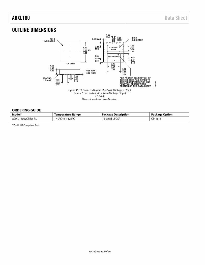
ADXL180 Data Sheet
Rev. B | Page 58 of 60
OUTLINE DIMENSIONS
080
408-
A
1.621.521.42
1.831.731.63
3.703.603.50
3.313.213.11
5.105.00 SQ4.90
1.501.451.40
TOP VIEW
0.05 MAX0.02 NOM
0.300.250.18
1.351.251.15
EXPOSEDPADS
(BOTTOM VIEW)
0.50BSC 0.25
BSC0.15 MAX
0.20MIN
0.500.400.30
PIN 1INDICATOR
SEATINGPLANE
PIN 1INDICATOR
FOR PROPER CONNECTION OFTHE EXPOSED PAD, REFER TOTHE PIN CONFIGURATION ANDFUNCTION DESCRIPTIONSSECTION OF THIS DATA SHEET.
Figure 45. 16-Lead Lead Frame Chip Scale Package [LFCSP] 5 mm × 5 mm Body and 1.45 mm Package Height
(CP-16-8) Dimensions shown in millimeters
ORDERING GUIDE Model1 Temperature Range Package Description Package Option ADXL180WCPZA-RL −40°C to +125°C 16-Lead LFCSP CP-16-8 1 Z = RoHS Compliant Part.

Data Sheet ADXL180
Rev. B | Page 59 of 60
NOTES

ADXL180 Data Sheet
Rev. B | Page 60 of 60
NOTES
©2008–2018 Analog Devices, Inc. All rights reserved. Trademarks and registered trademarks are the property of their respective owners.
D07544-0-1/18(B)