Embed Size (px)
Citation preview

CONFIDENTIAL bq77PL900
DRAFT SPECIFICATION Information in the data sheet could change at any time without notice.
2/15/2008 Copyright © 2007, Texas Instruments Incorporated
TEXAS INSTRUMENTS CONFIDENTIAL Page 1 of 61
FIVE to TEN SERIES CELL LITHIUM-ION OR LITHIUM-POLYMER BATTERY PROTECTION AND AFE IC
FEATURES • 5-,6-,7-,8-,9-, or 10 Series Cell Protection • PMOS FET Drive for Charge and Discharge FETs • Capable of operation with 1mΩ Sense Resistor • Supply Voltage Range from 7.0V to 50V • Low Supply Current of 150μA Typical • Integrated 5.0V 25-mA LDO • Integrated 3.3V 25-mA LDO Stand Alone Mode • Pack protection control and recovery • Individual cell monitoring • Integrated cell balancing • Programmable Threshold and Delay time for
• Over Voltage • Under Voltage • Over Current in Discharge • Short Circuit in Discharge
• Fixed Over Temperature Protection Host Control Mode • I2C Interface to Host Controller • Analog interface for Host cell measurement and
system Charge/Discharge current • Host controlled protection recovery • Host controlled cell balancing APPLICATIONS • Cordless Power Tools • Power Assisted bicycle and scooter • UPS • Medical equipments
DESCRIPTION The bq77PL900 is a five to ten series cell lithium-ion battery pack protector. With the integrated I2C communication interface it is also suitable as an analog front end (AFE) that incorporates two LDOs, one of 5.0V @ 25mA and a second of 3.3V @ 25mA to power a Host controller. The bq77PL900 integrates a voltage translation system to extract battery parameters such as individual cell voltages and charge/discharge current. Other parameters such as voltage protection thresholds and detection delay time can be programmed by using the internal EEPROM which increases the flexibility of the battery management system. The bq77PL900 primarily acts as a Stand Alone battery protection system (Stand Alone Mode). It can be combined with a micro controller to offer fuel gauge or other battery management capabilities to the Host system (Host Control Mode). The bq77PL900 provides full safety protection for over voltage, under voltage, over current in discharge and short circuit in discharge conditions. In safety conditions the bq77PL900 turns off the FET drive autonomously dependant on the internal EEPROM threshold and timing configuration setting. No external components are needed to configure the protection features. The analog outputs allow the host to observe individual cell voltages and charge/discharge current. Cell balancing of each cell can be performed autonomously or the host can control it via a cell bypass path integrated into the bq77PL900, which can be enabled via the internal control register accessible via the I2C like interface. The maximum bypass current is set via an external series resistor and internal FET on resistance (typ. 400Ω). Optionally, external bypass cell balance FETs could

CONFIDENTIAL bq77PL900
DRAFT SPECIFICATION Information in the data sheet could change at any time without notice.
2/15/2008 Copyright © 2007, Texas Instruments Incorporated
TEXAS INSTRUMENTS CONFIDENTIAL Page 2 of 61
1 TYPICAL IMPLEMENTATION
1.1 Stand Alone Mode
LDO, Thermal Output Drive
Pack +
Pack -
Discharge
Cell Balance Drive
Over Load Protection
Fuse
Over Voltage/Under Voltage Protection
bq29500
PCH FET Drive
RAM Registers
Sense Resistor
Short Current Protection
Charge
Serial Interface
LDO, Thermal Output Drive
Pack +
Pack -
Discharge
Cell Balance Drive
Over Load Protection
Fuse
Over Voltage/Under Voltage Protection
bq29500
PCH FET Drive
RAM Registers
Sense Resistor
Short Current Protection
Charge
Serial Interface

CONFIDENTIAL bq77PL900
DRAFT SPECIFICATION Information in the data sheet could change at any time without notice.
2/15/2008 Copyright © 2007, Texas Instruments Incorporated
TEXAS INSTRUMENTS CONFIDENTIAL Page 3 of 61
1.2 Host Control Mode
Serial Interface
Voltage OutputSafety and PowerManagementControl
Pack +
Pack-
Micro processor
Fuse
NTC
3.3Vor 5.0V
XRST
Sense Resistor
Battery Capacity Monitor
Cell balance Algorithm andControl
Thermal Measurement
Sirial Interface
RAM ROM
LDO, Thermal Output Drive
Cell Voltage Output, Cell Balance
Over Load Protection
Over Voltage/Under Voltage Protection
bq29500
PCH FET Drive
RAM Registers
Short Current Protection
Serial Interface
Serial Interface
Voltage OutputSafety and PowerManagementControl
Pack +
Pack-
Micro processor
Fuse
NTC
3.3Vor 5.0V
XRST
Sense Resistor
Battery Capacity Monitor
Cell balance Algorithm andControl
Thermal Measurement
Sirial Interface
RAM ROM
LDO, Thermal Output Drive
Cell Voltage Output, Cell Balance
Over Load Protection
Over Voltage/Under Voltage Protection
bq29500
PCH FET Drive
RAM Registers
Short Current Protection
Serial Interface
2 PIN DETAILS
2.1 Pin Descriptions
Pin # Name Description
1 CPOUT Charge pump output and Internal power source.
2 NC No Connect (not electrically connected)
3 CP4 Charge pump capacitor 1 connection terminal(GND)
4 CP3 Charge pump capacitor 1 connection terminal
5 CP2 Charge pump capacitor 2 connection terminal
6 CP1 Charge pump capacitor 2 connection terminal
7 NC No Connect (not electrically connected)
8 DSG Discharge FET gate drive
9 BAT Power supply voltage
10 VC1 Sense voltage input terminal for most positive cell, balance current input for most positive cell and battery stack measurement input

CONFIDENTIAL bq77PL900
DRAFT SPECIFICATION Information in the data sheet could change at any time without notice.
2/15/2008 Copyright © 2007, Texas Instruments Incorporated
TEXAS INSTRUMENTS CONFIDENTIAL Page 4 of 61
Pin # Name Description
11 VC2 Sense voltage input terminal for second most positive cell, balance current input for second most positive cell and return balance current for most positive cell.
12 VC3 Sense voltage input terminal for third most positive cell, balance current input for third most positive cell and return balance current for second most positive cell.
13 VC4 Sense voltage input terminal for fourth positive cell, balance current input for fourth positive cell and return balance current for third most positive cell.
14 VC5 Sense voltage input terminal for fifth positive cell, balance current input for fifth positive cell and return balance current for fourth most positive cell.
15 VC6 Sense voltage input terminal for sixth positive cell, balance current input for sixth positive cell and return balance current for fifth most positive cell.
16 VC7 Sense voltage input terminal for seventh positive cell, balance current input for seventh positive cell and return balance current for sixth most positive cell.
17 VC8 Sense voltage input terminal for eighth positive cell, balance current input for eighth positive cell and return balance current for seventh most positive cell.
18 VC9 Sense voltage input terminal for ninth positive cell, balance current input for ninth positive cell and return balance current for eighth most positive cell.
19 VC10 Sense voltage input terminal for tenth positive cell, balance current input for tenth positive cell and return balance current for ninth most positive cell.
20 VC11 Sense voltage input terminal for most negative cell, return balance current for least positive cell.
21 GND Power supply ground
22 SRBGND Current sense terminal( Connect Battery to cell’s GND)
23 SRPGND Current sense positive terminal when discharging relative to SRNGND, Current sense negative terminal when charging relative to SRGND,. (Connect to Pack GND)
24 EEPROM Active high EEPROM write enable pin. During normal operation should be connected to GND
25 XALERT Open-drain output used to indicate status register change. With an internal 100kΩ pull-up to VREG1or VREG2
26 SDATA Open-drain bi-directional serial interface data with an internal 10kΩ pull-up to VLOG
27 SCLK Open-drain bi-directional serial interface clock with an internal 10kΩ pull-up to VLOG
28 XRST Power on reset output. Active low open-drain output for micro processor
29 IOUT Amplifier output for charge/discharge current measurement
30 GND Power supply ground
31 VOUT Amplifier output for cell voltage measurement
32 VLOG Data I/O voltage set by connecting either VREG1 or VREG2
33 CNF0 Used cell for number determination in combination with CNF1 and CNF2
34 CNF1 Used cell for number determination in combination with CNF0 and CNF2
35 CNF2 Used cell for number determination in combination with CNF0 and CNF1
36 ZEDE Protection delay test pin. Minimizes protection delay times when connected to VLOG. Programmed delay times used when pulled to GND, normal operation.

CONFIDENTIAL bq77PL900
DRAFT SPECIFICATION Information in the data sheet could change at any time without notice.
2/15/2008 Copyright © 2007, Texas Instruments Incorporated
TEXAS INSTRUMENTS CONFIDENTIAL Page 5 of 61
Pin # Name Description
37 GND Power supply ground
38 TIN Temperature sensing input
39 TOUT Thermistor bias current source
40 VREG2 Integrated 3.3V regulator output
41 GND Should be connected system GND, not power supply GND
42 VREG1 Integrated 5.0V regulator output
43 NC No Connect (not electrically connected)
44 GPOD General purpose N-CH FET open drain output
45 NC No Connect (not electrically connected)
46 PMS Determines CHG output state for zero volt charge
47 PACK PACK positive terminal and alternative power source
48 CHG Charge FET gate drive

CONFIDENTIAL bq77PL900
DRAFT SPECIFICATION Information in the data sheet could change at any time without notice.
2/15/2008 Copyright © 2007, Texas Instruments Incorporated
TEXAS INSTRUMENTS CONFIDENTIAL Page 6 of 61
2.2 Pin Out Diagrams
DSG
CPOUT
CP4
2
7
6
5
4
3
36
35
34
33
32
31
30
8
9
10
11
12
29
28
27
26
48
13
14
47
1
NC
VC1
CNF2
PMS
VREG1
VC2
VC3
VREG2
VC4
VC5
XRST
VLOG
TOUT
VC6
PACK
GPOD
15
VC9
38
37
CHG
16
17
18
GND
VC10 19
VC11
46
45
44
43
CP3
VC7
CNF1
VC8
BAT
SDATA
SCLK
42
XALERT
GND
VOUT
20
SRBGND
21
22
23
CP1
SRPGND
24
CP2
41
40
39
25
IOUT
EEPROM
NC
NC
GND
GND
NC
ZEDE
CNF0
TIN
Package Dissipation Ratings
PACKAGE TA≤25°C POWER
RATING
DERATING FACTOR ABOVE
TA≥70°C
TA=85°C POWER
RATING
TA=100°C POWER
RATING
DL 1388mW 11.1mW/°C 720mW 555mW
3 ORDERING INFORMATION
PACKAGED TA
SSOP48
-40°C to 100°C bq77PL900DL
(1) The bq77PL900 can be ordered in tape and reel by adding the suffix R to the orderable part number, i.e., bq77PL900DLR.
CONFIDENTIAL bq77PL900
DRAFT SPECIFICATION Information in the data sheet could change at any time without notice.
2/15/2008 Copyright © 2007, Texas Instruments Incorporated
TEXAS INSTRUMENTS CONFIDENTIAL Page 7 of 61
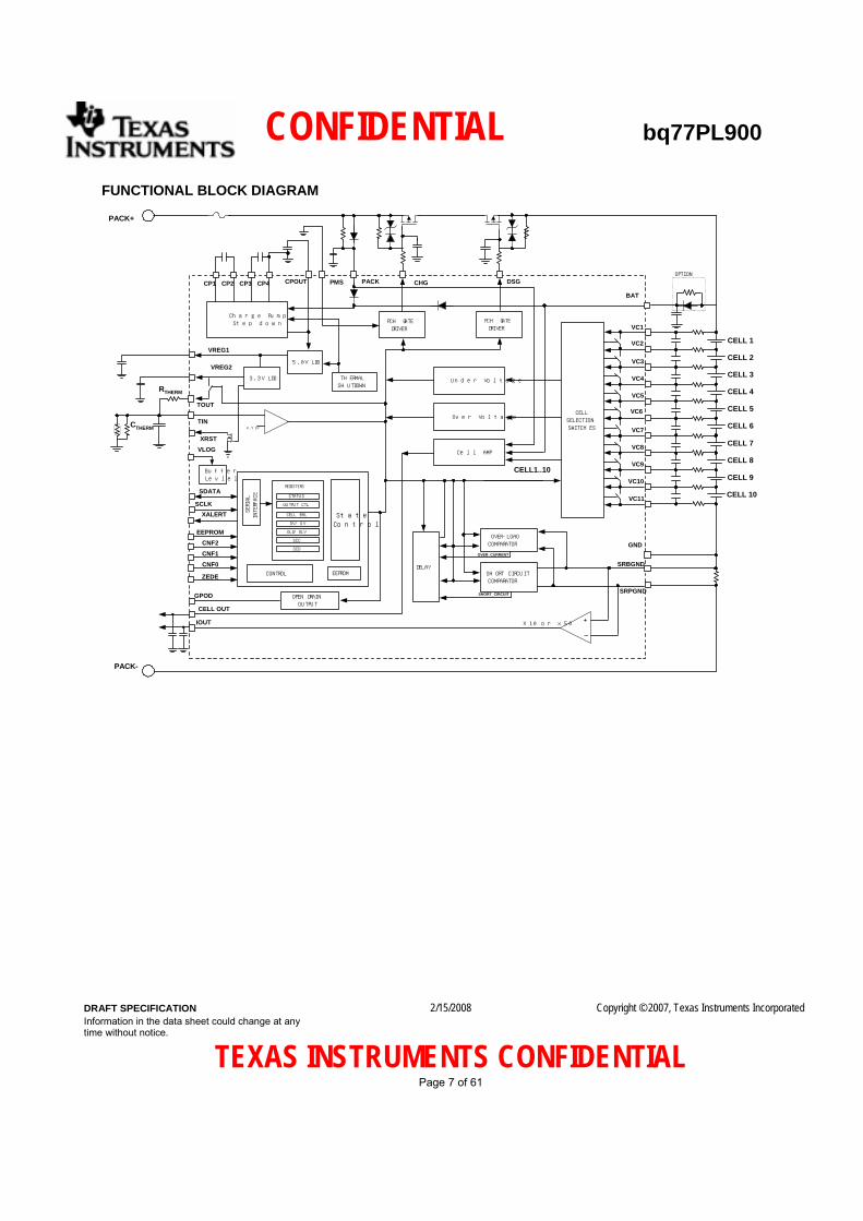
FUNCTIONAL BLOCK DIAGRAM
.
.
.
.GND
OVER_CURRENT
CELL1..10
SRBGND
SRPGND
OVER-LOADCOMPARATOR
SHORT CIRCUITCOMPARATOR
SHORT_CIRCUIT
DELAY
OPEN DRAINOUTPUT
GPOD
Under Voltage
CELLSELECTIONSWITCHES
PACK
PCH GATEDRIVER
CHG DSG
PACK-
VC7
VC8
VC11
CELL 8
CELL 7
VC9
VC10
CELL 10
CELL 9
XALERT
SDATA
SER
IAL
INTER
FA
CE
STATUS
OUTPUT CTL
OV/UV
OLD/OLV
SCC
SCD
REGISTERS
PACK+
VC3
VC4
CELL 4
CELL 3
VC5
CELL 6
CELL 5
CELL 2
CELL 1
VC6
VC1
VC2
Charge PumpStep down
TOUT
CTHERM
VREG1
5.0V LDO
RTHERM
3.3V LDO
VREG2
SCLKCELL BAL State
Control
+X10 or x50IOUT
XRST
CP1 CP2 CP3 CP4
EEPROM
¥
THERMALSHUTDOWN
VLOG
BufferLevlel
CPOUT
Cell AMP
CELL OUT
BAT
PCH GATEDRIVER
Over Voltage
0.98V
CONTROL EEPROM
CNF2CNF1CNF0
ZEDE
TIN
OPTION
PMS

CONFIDENTIAL bq77PL900
DRAFT SPECIFICATION Information in the data sheet could change at any time without notice.
2/15/2008 Copyright © 2007, Texas Instruments Incorporated
TEXAS INSTRUMENTS CONFIDENTIAL Page 8 of 61
4 SAFETY STATE OVERVIEW
4.1 Stand Alone Mode
No Power Supply
UVLO Mode
CHG: OFFDSG: OFFVREG1: OFF
XRST: LOWI2C :Disabled
Power Supply to PACK
Normal Mode
V < 2.3VV REG2> 2.4V
Current Protection ModeDis-charge side
Attach a Charger
VREG2: OFF
CHG: OFFDSG: OFFVREG1: ON
XRST: HIGHI2C :Enabled
VREG2: ON
Over voltageProtection Mode
CHG: OFFDSG: ON
CHG: ONDSG: ON
VREG1: ON
XRST: HighI2C :Enabled
VREG2: ON
Vcell > VOV All cell voltage < Vov –ΔVov
Under voltageProtection Mode
VREG1: ON
XRST: HighI2C :Enabled
VREG2: ON
CHG: ONDSG: OFFVREG1: ON
XRST: HighI2C :Enabled
VREG2: ON
Vcell < VUV
REG2
Stand Alone Mode
All cell voltage >Vuv +ΔVuvOr((Vpack-Vbat>0.4V and All cell voltge >Vuv ))
Over temp Protection Mode
CHG: OFFDSG: OFFVREG1: ON
XRST: HIGHI2C :Enabled
VREG2: ON
< 0.975VVIN
> 1.075VVIN
UV Protection: Disabled
Current Protection: DisabledThermal Protection: Disabled
OV Protection: Disabled
UV Protection: Enabled
Current Protection: EnabledThermal Protection: Enabled
OV Protection: Enabled
UV Protection: Enabled
Current Protection: EnabledThermal Protection: Enabled
OV Protection: Disabled
UV Protection: Enabled
Current Protection: DisabledThermal Protection: Enabled
OV Protection: Enabled
UV Protection: Enabled
Current Protection: EnabledThermal Protection: Disabled
OV Protection: Enabled
UV Protection: Disabled
Current Protection: EnabledThermal Protection: Enabled
OV Protection: Enabled
Shutdown ModeCHG: OFFDSG: OFFVREG1: OFF
I2C: DisabledCurrent Protection: DisabledVCELL: DisabledWatchdog: DisabledThermal Protection: Disabled
VREG2: OFFXRST: LOW
Power Supply to PACK
No Supply to PACK
VSR > VOCor VSC for a period of t OC or t SC
No Power Supply
UVLO Mode
CHG: OFFDSG: OFFVREG1: OFF
XRST: LOWI2C :Disabled
Power Supply to PACK
Normal Mode
V < 2.3VV REG2> 2.4V
Current Protection ModeDis-charge side
Attach a Charger
VREG2: OFF
CHG: OFFDSG: OFFVREG1: ON
XRST: HIGHI2C :Enabled
VREG2: ON
Over voltageProtection Mode
CHG: OFFDSG: ON
CHG: ONDSG: ON
VREG1: ON
XRST: HighI2C :Enabled
VREG2: ON
Vcell > VOV All cell voltage < Vov –ΔVov
Under voltageProtection Mode
VREG1: ON
XRST: HighI2C :Enabled
VREG2: ON
CHG: ONDSG: OFFVREG1: ON
XRST: HighI2C :Enabled
VREG2: ON
Vcell < VUV
REG2
Stand Alone Mode
All cell voltage >Vuv +ΔVuvOr((Vpack-Vbat>0.4V and All cell voltge >Vuv ))
Over temp Protection Mode
CHG: OFFDSG: OFFVREG1: ON
XRST: HIGHI2C :Enabled
VREG2: ON
< 0.975VVIN
> 1.075VVIN
UV Protection: Disabled
Current Protection: DisabledThermal Protection: Disabled
OV Protection: DisabledUV Protection: Disabled
Current Protection: DisabledThermal Protection: Disabled
OV Protection: Disabled
UV Protection: Enabled
Current Protection: EnabledThermal Protection: Enabled
OV Protection: EnabledUV Protection: Enabled
Current Protection: EnabledThermal Protection: Enabled
OV Protection: Enabled
UV Protection: Enabled
Current Protection: EnabledThermal Protection: Enabled
OV Protection: DisabledUV Protection: Enabled
Current Protection: EnabledThermal Protection: Enabled
OV Protection: Disabled
UV Protection: Enabled
Current Protection: DisabledThermal Protection: Enabled
OV Protection: EnabledUV Protection: Enabled
Current Protection: DisabledThermal Protection: Enabled
OV Protection: Enabled
UV Protection: Enabled
Current Protection: EnabledThermal Protection: Disabled
OV Protection: EnabledUV Protection: Enabled
Current Protection: EnabledThermal Protection: Disabled
OV Protection: Enabled
UV Protection: Disabled
Current Protection: EnabledThermal Protection: Enabled
OV Protection: EnabledUV Protection: Disabled
Current Protection: EnabledThermal Protection: Enabled
OV Protection: Enabled
Shutdown ModeCHG: OFFDSG: OFFVREG1: OFF
I2C: DisabledCurrent Protection: DisabledVCELL: DisabledWatchdog: DisabledThermal Protection: Disabled
VREG2: OFFXRST: LOW
Power Supply to PACK
No Supply to PACK
VSR > VOCor VSC for a period of t OC or t SC
4.2 Stand Alone STATUS bit, XALERT and FET Transition Summary MODE TRANSITION STATUS BIT XALERT FET ACTIVITY Normal to Current Protection SCD or OCD = 1 H to L DSG and CHG off Current Protection to Normal SCD or OCD = 0 L to H DSG and CHG on Normal to Over Voltage Protection OVP = 1 H to L CHG off Over Voltage Protection to Normal OVP = 0 L to H CHG on Normal to Under Voltage Protection (When VAPCK goes down to 0V, move to shutdown mode)
UVP = 1 H to L DSG off
Under Voltage Protection to Normal UVP = 0 L to H DSG on Normal to Over temperature OVT=1 H to L DSG and CHG off Over temperature to Normal OVT=0 L to H DSG and CHG on
CONFIDENTIAL bq77PL900
DRAFT SPECIFICATION Information in the data sheet could change at any time without notice.
2/15/2008 Copyright © 2007, Texas Instruments Incorporated
TEXAS INSTRUMENTS CONFIDENTIAL Page 9 of 61
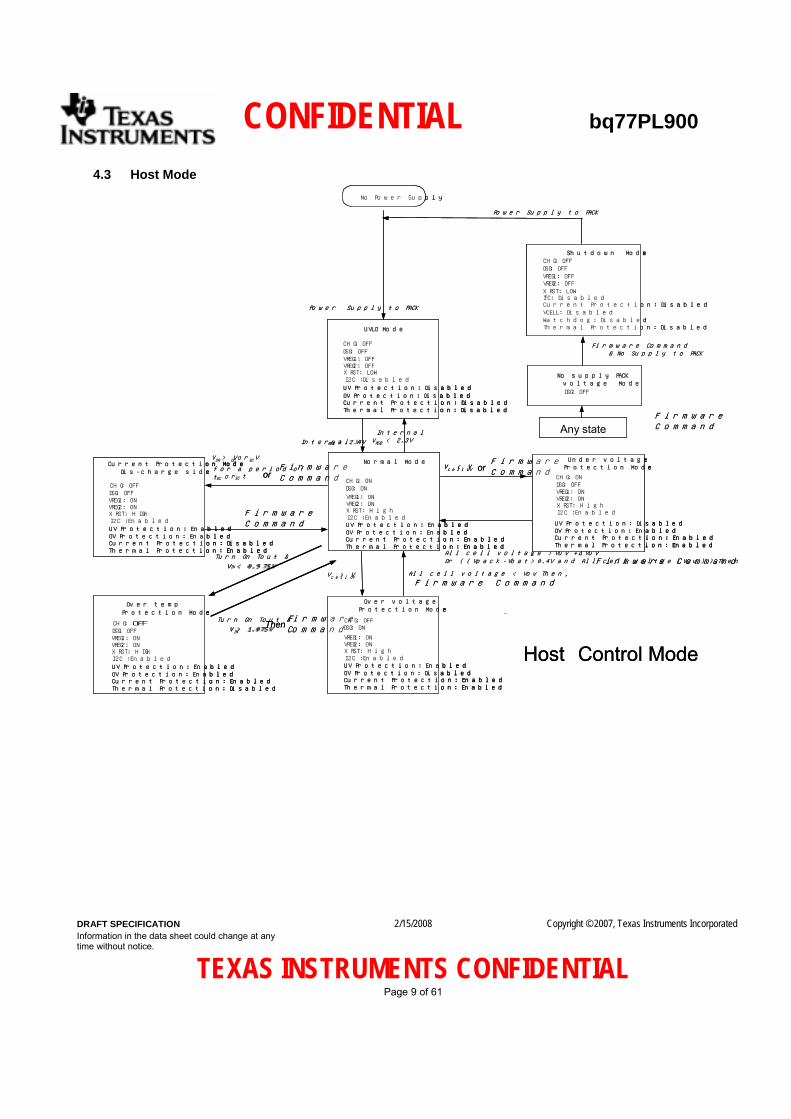
4.3 Host Mode No Power Supply
UVLO Mode
CHG: OFFDSG: OFFVREG1: OFF
XRST: LOWI2C :Disabled
Power Supply to PACK
Normal Mode
InternalV < 2.3VInternal VREG2> 2.4V
Current Protection ModeDis-charge side
VSR > VOCor VSC
for a period of t OC or t SC
VREG2: OFF
CHG: OFFDSG: OFFVREG1: ON
XRST: HIGHI2C :Enabled
VREG2: ON
Over voltageProtection Mode
CHG: OFFDSG: ON
CHG: ONDSG: ON
VREG1: ON
XRST: HighI2C :Enabled
VREG2: ON
Vcell > VOV
Under voltageProtection Mode
VREG1: ON
XRST: HighI2C :Enabled
VREG2: ON
CHG: ONDSG: OFFVREG1: ON
XRST: HighI2C :Enabled
VREG2: ON
REG2
Power Supply to PACK
Shutdown ModeCHG: OFFDSG: OFFVREG1: OFF
I2C: DisabledCurrent Protection: DisabledVCELL: DisabledWatchdog: DisabledThermal Protection: Disabled
Firmware Command& No Supply to PACK
VREG2: OFF
DSG: OFF
No supply PACKvoltage Mode
DSG: OFF
Any state
Host Control Mode
XRST: LOW
Over temp Protection Mode
CHG: OFFDSG: OFFVREG1: ON
XRST: HIGHI2C :Enabled
VREG2: ON
< 0.975VVIN
UV Protection: Disabled
Current Protection: DisabledThermal Protection: Disabled
OV Protection: Disabled
UV Protection: Enabled
Current Protection: EnabledThermal Protection: Enabled
OV Protection: Enabled
UV Protection: Enabled
Current Protection: EnabledThermal Protection: Enabled
OV Protection: Disabled
UV Protection: Enabled
Current Protection: DisabledThermal Protection: Enabled
OV Protection: Enabled
UV Protection: Enabled
Current Protection: EnabledThermal Protection: Disabled
OV Protection: Enabled
UV Protection: Disabled
Current Protection: EnabledThermal Protection: Enabled
OV Protection: Enabled
FirmwareCommand
Vcell < VUV
Then
FirmwareCommand
Firmware Command
Firmware Command
FirmwareCommand
FirmwareCommand
orFirmwareCommand
Turn On Tout &
> 1.075VVIN
Turn On Tout &
All cell voltage < Vov Then,
or
All cell voltage >Vuv +ΔVuvOr ((Vpack-Vbat>0.4V and All cell voltge <Vuv ) ),Then
No Power Supply
UVLO Mode
CHG: OFFDSG: OFFVREG1: OFF
XRST: LOWI2C :Disabled
Power Supply to PACK
Normal Mode
InternalV < 2.3VInternal VREG2> 2.4V
Current Protection ModeDis-charge side
VSR > VOCor VSC
for a period of t OC or t SC
VREG2: OFF
CHG: OFFDSG: OFFVREG1: ON
XRST: HIGHI2C :Enabled
VREG2: ON
Over voltageProtection Mode
CHG: OFFDSG: ON
CHG: ONDSG: ON
VREG1: ON
XRST: HighI2C :Enabled
VREG2: ON
Vcell > VOV
Under voltageProtection Mode
VREG1: ON
XRST: HighI2C :Enabled
VREG2: ON
CHG: ONDSG: OFFVREG1: ON
XRST: HighI2C :Enabled
VREG2: ON
REG2
Power Supply to PACK
Shutdown ModeCHG: OFFDSG: OFFVREG1: OFF
I2C: DisabledCurrent Protection: DisabledVCELL: DisabledWatchdog: DisabledThermal Protection: Disabled
Firmware Command& No Supply to PACK
VREG2: OFF
DSG: OFF
No supply PACKvoltage Mode
DSG: OFF
Any state
Host Control Mode
XRST: LOW
Over temp Protection Mode
CHG: OFFDSG: OFFVREG1: ON
XRST: HIGHI2C :Enabled
VREG2: ON
< 0.975VV < 0.975VVIN
UV Protection: Disabled
Current Protection: DisabledThermal Protection: Disabled
OV Protection: DisabledUV Protection: Disabled
Current Protection: DisabledThermal Protection: Disabled
OV Protection: Disabled
UV Protection: Enabled
Current Protection: EnabledThermal Protection: Enabled
OV Protection: EnabledUV Protection: Enabled
Current Protection: EnabledThermal Protection: Enabled
OV Protection: Enabled
UV Protection: Enabled
Current Protection: EnabledThermal Protection: Enabled
OV Protection: DisabledUV Protection: Enabled
Current Protection: EnabledThermal Protection: Enabled
OV Protection: Disabled
UV Protection: Enabled
Current Protection: DisabledThermal Protection: Enabled
OV Protection: EnabledUV Protection: Enabled
Current Protection: DisabledThermal Protection: Enabled
OV Protection: Enabled
UV Protection: Enabled
Current Protection: EnabledThermal Protection: Disabled
OV Protection: EnabledUV Protection: Enabled
Current Protection: EnabledThermal Protection: Disabled
OV Protection: Enabled
UV Protection: Disabled
Current Protection: EnabledThermal Protection: Enabled
OV Protection: EnabledUV Protection: Disabled
Current Protection: EnabledThermal Protection: Enabled
OV Protection: Enabled
FirmwareCommand
Vcell < VUVVcell < VUV
Then
FirmwareCommand
Firmware Command
Firmware Command
FirmwareCommand
FirmwareCommand
orFirmwareCommand
Turn On Tout &
> 1.075VV > 1.075VVIN
Turn On Tout &
All cell voltage < Vov Then,
or
All cell voltage >Vuv +ΔVuvOr ((Vpack-Vbat>0.4V and All cell voltge <Vuv ) ),Then

CONFIDENTIAL bq77PL900
DRAFT SPECIFICATION Information in the data sheet could change at any time without notice.
2/15/2008 Copyright © 2007, Texas Instruments Incorporated
TEXAS INSTRUMENTS CONFIDENTIAL Page 10 of 61
4.4 Host Control Summary
MODE TRANSITION Function and Firm ware Procedure Normal to Current protection
Vsr > Voc or Vsc for period of toc or tsc Automatically, DSG and CHG turn off , SCD or OCD status changes=1, XALERT=L
Current protection to Normal
1.Send commands to transition LTCLR from 0 to 1 to 0 2. Read status bit. XALERT would change to H. 3.Set CHG and DSG FET ON to enable normal operation
Normal to Over voltage protection
Vcell > Vov for period of tov Automatically, CHG turns off, UV status changes=1,XALERT=L
Over voltage protection to Normal
1.Confirm the OVP protection status is cleared 2. Send command LTCLR from 1 to 0 3. Read status bit. XALERT would change to H. 4.Set CHG FET ON to enable normal operation
UVFET_DIS=0 Vcell < Vuv for period of tuv Automatically, DSG turns off, UV status changes=1,XALERT=L
Normal to Undervoltage protection
UVFET_DIS=1 1.Vcell < Vuv or for period of tuv, UV status changes=1,XALERT=L 2. Send commands to turn off DSG .
Under voltage protection to Normal
UVFET_DIS=X
1.Confirm the OVP protection status is cleared 2. Send command LTCLR from 1 to 0 3.Set DSG FET ON to enable normal operation 4. Read status bit. XALERT would change to H.
Normal to Over temperature
1. Send commands to turn on TOUT 2. If TIN voltage <0.975V, DSG and CHG turn off , OVTEMP status changes=1,XALERT=L
Over temperature to Normal 1. Send commands to turn on TOUT (To return to Normal mode, bq77PL900 needs to acknowledge Vth > 1.075V ) 2.Send commands to transition LTCLR from 1 to 0 3.Set CHG and DSG FET ON 4. Read status bit. XALERT would change to H.
Any mode to Shut down 1.Set DSG FET OFF 2. Wait PACK voltage goes down to 0V 3.SET shut down bit to “1”

CONFIDENTIAL bq77PL900
DRAFT SPECIFICATION Information in the data sheet could change at any time without notice.
2/15/2008 Copyright © 2007, Texas Instruments Incorporated
TEXAS INSTRUMENTS CONFIDENTIAL Page 11 of 61
ABSOLUTE MAXIMUM RATINGS Over operating free–air temperature range (unless otherwise noted)†
Supply voltage range, VMAX BAT, PACK -0.3 to 60V
VC1~ VC10 -0.3 to 60V
VC11 0.3 to 5.0V
VCn to VCn+1, n=1 to 10 -0.3 to 6.0V
PMS -0.3 to 60V
SRP, SRN –0.5 to 1.0V
Input voltage range, VIN
SDATA, SCLK, EEPROM, VLOG, ZEDE, CNF0, CNF1, CNF2, TIN -0.3 V to 7.0 V
CHG PACK-20 to 60v
DSG BAT-20 to 60v
TOUT, VOUT, IOUT, XRST, XALERT, SDATA, SCLK -0.3 V to 7.0 V Output voltage range, VO
CP1, CP2, CP3, CP4, CPOUT, GPOD -0.3 to 60V
Current for cell balancing, ICB 10mA
Storage temperature range, TSTG –65 to 150°C
Lead temperature (soldering, 10 s), TSOLDER 300°C
† Stresses beyond those listed under “absolute maximum ratings” may cause permanent damage to the device. These are stress ratings only, and functional operation of the device at these or any other conditions beyond those indicated under “recommended operating conditions” is not implied. Exposure to absolute–maximum–rated conditions for extended periods may affect device reliability.
Note 1: All voltages are with respect to ground of this device except VCn-VC(n+1), where n=1 to 10 cell voltage
5 RECOMMENDED OPERATING CONDITIONS PARAMETER MIN NOM MAX UNIT
Supply Voltage PACK, BAT 7.0 50 V
VI(STARTUP) Start up voltage PACK 7.5 V
VLOG Logic supply voltage 0.8*VREG2 1.2*VR
EG1
V
VC1 to VC10 0 BAT
VC11 0 0.5
SRP, SRN -0.3 0.5
VCn – VC(n+1), (n=1 to 10 ) 0 5.0
VI Input voltage range
PACK, BAT 50
V
VIH Logic level input voltage high 0.8*VLOG VLOG
VIL Logic level input voltage low
SCLK, SDATA, EEPROM, VLOG
(VLOG = VREG1 or VREG2) 0 0.2*VL
OG
XALERT, SDATA VLOG
VGAIN=High 1.2
VO Output voltage range
VOUT, IOUT VGAIN=Low 0.975
V
CONFIDENTIAL bq77PL900
DRAFT SPECIFICATION Information in the data sheet could change at any time without notice.
2/15/2008 Copyright © 2007, Texas Instruments Incorporated
TEXAS INSTRUMENTS CONFIDENTIAL Page 12 of 61
PARAMETER MIN NOM MAX UNIT
GPOD 45 V
RVCX 400 Ω
CREG1 External 5.0V REG capacitor 2.2 µF
CREG2 External 3.3V REG capacitor 2.2 µF
CCP1, CCP2
Charge pump flying capacitor 1.0 µF
CCPOUT Charge pump output capacitor
4.7 µF
CVOUT Output capacitance 0.1 µF
CIOUT Output capacitance 0.1 µF
IOL GPOD, XRST 1 mA
fSCLK Input Frequency SCLK 100 KHz
EEPROM number of writes 3
TOPR Operating Temperature -25 85 °C
TFUNC Functional Temperature -40 100 °C
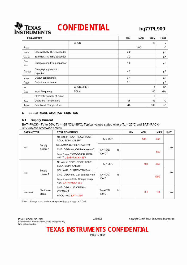
6 ELECTRICAL CHARACTERISTICS
6.1 Supply Current BAT=PACK= 7V to 50V, TA = -25 ºC to 85ºC, Typical values stated where TA = 25ºC and BAT=PACK= 36V (unless otherwise noted)
PARAMETER TEST CONDITION MIN NOM MAX UNIT
TA = 25°C 500 750
ICC1 Supply current 1
No load at REG1, REG2, TOUT, SCLK, SDIN, XALERT
CELLAMP, CURRENTAMP=off
CHG, DSG= on, Cell balance = off
IREG1 = IREG2 =0mA,Charge pump =off (1) , BAT=PACK= 35V
TA=-40°C to 100°C
850
µA
TA = 25°C 750 950
ICC2 Supply current 2
No load at REG1, REG2, TOUT, SCLK, SDIN, XALERT
CELLAMP, CURRENTAMP=on
CHG, DSG= on, Cell balance = off
IREG1 = IREG2 =0mA, Charge pump =off, BAT=PACK= 35V
TA=-40°C to 100°C
1250 µA
ISHUTDOWN Shutdown Mode
CHG, DSG = off, VREG1= VREG2=off,
PACK = 0V, BAT = 35V
TA=-40°C to 100°C
0.1 1.0 µA
Note 1: Charge pump starts working when (IREG33 + IREG5) > 3.0mA

CONFIDENTIAL bq77PL900
DRAFT SPECIFICATION Information in the data sheet could change at any time without notice.
2/15/2008 Copyright © 2007, Texas Instruments Incorporated
TEXAS INSTRUMENTS CONFIDENTIAL Page 13 of 61
6.2 VREG1, Integrated 5.0V LDO BAT=PACK= 7V to 50V, TA = -25 ºC to 85ºC, Typical values stated where TA = 25ºC and BAT=PACK= 36V (unless otherwise noted)
PARAMETER TEST CONDITION MIN NOM MAX UNIT
8.5V < PACK or BAT ≤ 50V,
IOUT ≤ 25mA 4.55 5.0 5.45 V
V(REG1) Output voltage 7.0V < PACK or BAT ≤ 8.5V,
IOUT ≤ 3mA
TA=-40°C to 100°C
4.55 5.0 5.45 V
∆V(REG1) Output temperature drift PACK or BAT=50V IOUT = 2mA, TA = 25°C
±0.2 %
∆V(REG1LINE) Line regulation 10V ≤ PACK or BAT≤ 50V,
IOUT=2mA, TA = 25°C 10 20 mV
PACK or BAT = 36V,
0.2mA ≤ IOUT ≤ 2mA, TA = 25°C 7 15 mV
∆V(REG1LOAD) Load regulation PACK or BAT = 36V, 0.2mA ≤ IOUT ≤ 25mA, TA = 25°C
40 100 mV
PACK or BAT = 36V, VREG1 = 4.5V ,TA = 25°C 35 75 125 IREG1MAX Curent limit
PACK or BAT = 36V, VREG1 = 0V ,TA = 25°C 5 20 35
mA
mA
6.3 VREG2, Integrated 3.3V LDO BAT=PACK= 7V to 50V, TA = -25 ºC to 85ºC, Typical values stated where TA = 25ºC and BAT=PACK= 36V (unless otherwise noted)
PARAMETER TEST CONDITION MIN NOM MAX UNIT
7.0V < PACK or BAT ≤ 50V,
IOUT ≤ 25mA TA=-40°C to 100°C
3.05 3.3 3.55 V
V(REG2) Output voltage 7.0V < PACK or BAT ≤ 50V,
IOUT = 0.2mA TA=-40°C to 100°C
-2% 3.3 +2% V
∆V(REG2) Output temperature drift PACK or BAT = 50V IOUT = 2mA,
TA=-40°C to 100°C
±0.2 %
∆V(REG2) Line regulation 7.0V ≤ PACK or BAT≤ 50V,
IOUT=2mA, TA=25°C 10 20 mV
PACK or BAT=36V, 0.2mA ≤ IOUT ≤ 2mA, TA=25°C
7 15 mV
∆V(REG2) Load regulation PACK or BAT=36V, 0.2mA ≤IOUT ≤ 25mA, TA=25°C
40 100 mV
PACK or BAT = 36V, VREG2 = 3.0V ,TA=25°C 25 50 100 mA IREG2MAX Current limit
PACK or BAT = 36V, VREG2 = 0.0V ,TA=25°C 10 20 30 mA

CONFIDENTIAL bq77PL900
DRAFT SPECIFICATION Information in the data sheet could change at any time without notice.
2/15/2008 Copyright © 2007, Texas Instruments Incorporated
TEXAS INSTRUMENTS CONFIDENTIAL Page 14 of 61
6.4 TOUT, Thermistor Power Supply BAT=PACK= 7V to 50V, TA = -25 ºC to 85ºC, Typical values stated where TA = 25ºC and BAT=PACK= 36V (unless otherwise noted)
PARAMETER TEST CONDITION MIN NOM MAX UNIT
VTOUT IOUT = 0mA, TA = -40°C to 100°C 3.05 3.55 V
RDS(ON) Pass-element series resistance
IOUT = -1mA at TOUT pin, RDS(ON) = (VREG2 – VTOUT) / 1mA, TA = -40°C to 100°C, Ireg2=-0.2mA
50 100 Ω
VTINS Thermistor sense voltage
TA=-40°C to 100°C -5% 0.975 +5% V
VTINSHYS Thermistor sense hysteresis voltage
TA=-40°C to 100°C 50 100 150 mV
6.5 Thermal Shutdown BAT=PACK= 7V to 50V, TA = -25 ºC to 85ºC, Typical values stated where TA = 25ºC and BAT=PACK= 36V (unless otherwise noted)
ARAMETER TEST CONDITION MIN NOM MAX UNIT
Ttherm Shutdown threshold PACK or BAT = 36V (1) TBD 150 TBD ºC Note 1: Not 100% tested, guaranteed by design up to 125ºC
6.6 PMS, Pre-charge Mode Select Disable BAT=PACK= 7V to 50V, TA = -25 ºC to 85ºC, Typical values stated where TA = 25ºC and BAT=PACK= 36V (unless otherwise noted)
PARAMETER TEST CONDITION MIN NOM MAX UNIT
VPMSDISABLE PMS disable threshold of BAT
PACK = PMS=20V, VREG2=0V,
CHG=ON ->OFF 8 13 16 V
6.7 POR, Power On Reset BAT=PACK= 7V to 50V, TA = -25 ºC to 85ºC, Typical values stated where TA = 25ºC and BAT=PACK= 36V (unless otherwise noted)
PARAMETER TEST CONDITION MIN NOM MAX UNIT
VLOG=VREG1(5.0V)V 3.85 4.05 4.25 V VPOR- Negative-going voltage input
VLOG=VREG2(3.3V)V 2.55 2.65 2.75 V
VLOG = 3.3V 50 150 250 mv VPOR_HYS Positive-going hystersis
VLOG = 5.0V 100 250 400 mV
tRST Reset delay time 1 5 ms
6.8 Cell Voltage Monitor BAT=PACK= 7V to 50V, TA = -25 ºC to 85ºC, Typical values stated where TA = 25ºC and BAT=PACK= 36V (unless otherwise noted)
PARAMETER TEST CONDITION MIN NOM MAX UNIT
VCELL OUT CELL output VCn– VCn+1= 0V , 20V ≤ BAT ≤50V, VGAIN=Low TBD 0.975 TBD V

CONFIDENTIAL bq77PL900
DRAFT SPECIFICATION Information in the data sheet could change at any time without notice.
2/15/2008 Copyright © 2007, Texas Instruments Incorporated
TEXAS INSTRUMENTS CONFIDENTIAL Page 15 of 61
VCn– VCn+1= 0V , 20V ≤ BAT ≤50V, VGAIN=High TBD 1.200 TBD
VCn– VCn+1 = 4.5V , 20V ≤ BAT ≤50V 0.3
REF 1 CELL output Mode (Note1), 20V ≤ BAT or PACK ≤50V, VGAIN =Low
-2% 0.975 +2% V
REF 2 CELL output Mode (Note2), 20V ≤ BAT or PACK ≤50V, VGAIN =High
-2% 1.200 +2% V
PACK CELL output Mode (Note3) -5% PACK/50 +5% V
BAT CELL output Mode (Note4) -5% BAT/50 +5% V
CMRR Common Mode Rejection CELL max to CELL min,
20V ≤ BAT ≤50V 40 dB
K=CELL output (VC11=0.0 V, VC10=4.5V)
-CELL output (VC11=VC10=0.0V) / 4.5 (Note5) 0.147 0.150 0.153
K1 CELL scale factor 1 K=CELL output (VC2=40.5V, VC1=45.0V)
-CELL output (VC2=VC1=40.5V) / 4.5 (Note5) 0.147 0.150 0.153
K=CELL output (VC11=0.0V, VC10=4.5V)
-CELL output (VC11=VC10=0.0V) / 4.5 (Note6) 0.197 0.201 0.205
K2 CELL scale factor 2 K=CELL output (VC2=40.5V, VC1=45.0V)
-CELL output (VC2=VC1=40.5V) / 4.5 (Note6) 0.197 0.201 0.205
IVCELLOUT Drive current VCn– VCn+1= 0V , Vcell = 0V Ta=-40 to 100°C 12 18 µA
VICR CELL output offset error CELL output (VC2=45.0V, VC1=45.0V)
-CELL output (VC2=VC1=0.0V) -1 mV
RBAL Cell Balance internal resistance
RDS(ON) for internal FET switch at VDS = 2.0V,
BAT=PACK= 35V -50% 400 +50% Ω
Note 1 : STATE_CONTROL [VGAIN] = 0, FUNCTION_CONTROL [VAEN] = 1, CELL_SEL[CAL2] = 0,[CAL0] =1, [CAL0] = 1 Note 2 : STATE_CONTROL [VGAIN] = 1, FUNCTION_CONTROL [VAEN] = 1, CELL_SEL[CAL2] = 0,[CAL0] =1, [CAL0] = 1 Note 3 : STATE_CONTROL [VGAIN] = X, FUNCTION_CONTROL [PACK]=1,[VAEN] = 1, Note 4 : STATE_CONTROL [VGAIN] = X, FUNCTION_CONTROL [BAT]=1,[VAEN] = 1, Note 5 : STATE_CONTROL [VGAIN] = 0, FUNCTION_CONTROL [VAEN] = 1, CELL_SEL[CAL2] = 0,[CAL0] =0, [CAL0] = 0 Note 6 : STATE_CONTROL [VGAIN] = 1, FUNCTION_CONTROL [VAEN] = 1, CELL_SEL[CAL2] = 0,[CAL0] =0, [CAL0] = 0
6.9 Current Monitor BAT=PACK= 7V to 50V, TA = -25 ºC to 85ºC, Typical values stated where TA = 25ºC and BAT=PACK= 36V (unless otherwise noted)
PARAMETER TEST CONDITION MIN NOM MAX UNIT
VCELL_OFF Input offset voltage VSRP = VSRN = 0V (Note 1) 1.2 V
VIOUT_OFF_DRIFT Input offset voltage drift VSRP = VSRN = 0V (Note 1) -3 3 mV
DC gain Low (Note 2) -100mV < SRP < +100mV -2% 10 +2%
DC gain High (Note 3) -20mV < SRP < +20mV -2% 50 +2%
IIOUTOUT Drive current VIOUT= 0.0V
TA=-40 to 100ºC 12 18 µA
Note 1 : STATE_CONTROL [IGAIN] = X, FUNCTION_CONTROL [IAEN] = 1, [IACAL] = 1 Note 2 : STATE_CONTROL [IGAIN] = 0, FUNCTION_CONTROL [IAEN] = 1, [IACAL] = 0

CONFIDENTIAL bq77PL900
DRAFT SPECIFICATION Information in the data sheet could change at any time without notice.
2/15/2008 Copyright © 2007, Texas Instruments Incorporated
TEXAS INSTRUMENTS CONFIDENTIAL Page 16 of 61
Note 3: STATE_CONTROL [IGAIN] = 1, FUNCTION_CONTROL [IAEN] = 1, [IACAL] = 0
6.10 Battery Protection Thresholds BAT=PACK= 7V to 50V, TA = -25 ºC to 85ºC, Typical values stated where TA = 25ºC and BAT=PACK= 36V (unless otherwise noted)
PARAMETER TEST CONDITION MIN NOM MAX UNIT
VOV OV detection threshold range Default 4.15 4.50 V
∆VOV OV detection threshold program step 50 mV
VOVH OV detection hysteresis voltage range Default 0.1 0.4 V
ΔVOVH OV detection hysteresis program step 0.1 V
VUV UV detection threshold range Default 1.40 2.90 V
ΔVUV UV detection threshold program step 100 mV
VUVH UV detection hysteresis voltage Default 0.2 1.2 V
∆VUVH UV detection threshold program step 200 mV
VOCDT OCD detection threshold range Default 10 85 mV
∆VOCDT OCD detection threshold program step 5.0 mV
VSCDT SCD detection threshold range Default 60 135 mV
∆VSCDT SCD detection threshold program step 5.0 mV
VOV_acr OV detection threshold accuracy Default (TA = 0 to 85) -50 0 +50 mV
VUV_acr UV detection threshold accuracy Default -100 0 +100 mV
VOCD_acr OCD detection threshold accuracy Default -20 0 +20 %
VSCD_acr SCD detection threshold accuracy Default -20 0 +20 %
6.11 Battery Protection Delay Times BAT=PACK= 7V to 50V, TA = -25 ºC to 85ºC, Typical values stated where TA = 25ºC and BAT=PACK= 36V (unless otherwise noted)
PARAMETER TEST CONDITION MIN NOM MAX UNIT
tOV OV detection delay time range Default 500 2250 ms
∆tOV OV detection delay time step 250 ms
tUV UV detection delay time range Default 0 8000 ms
∆tUV UV detection delay time step 1.25 1000 ms
tOCD OCD detection delay time range Default 20 1600 ms
∆tOCD OCD detection delay time step 20 100 ms
tSCD SCD detection delay time range Default 0 900 µs
∆tSCD SCD detection threshold program step 60 µs
tOV_acr OV detection delay time accuracy Default -15 0 15 %
tUV_acr UV detection delay time accuracy Default -15 0 15 %
tOC_acr OC detection delay time accuracy Default -15 0 15 %
VSCD_acr SC detection delay time accuracy tSCD Max -15 0 15 %
tSRC OC/SC recovery timing at Stand Alone Mode -15 12.8sec 15 %
CONFIDENTIAL bq77PL900
DRAFT SPECIFICATION Information in the data sheet could change at any time without notice.
2/15/2008 Copyright © 2007, Texas Instruments Incorporated
TEXAS INSTRUMENTS CONFIDENTIAL Page 17 of 61
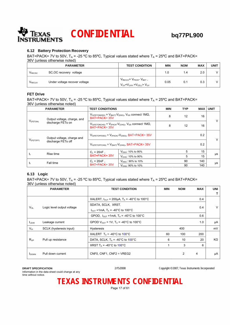
6.12 Battery Protection Recovery BAT=PACK= 7V to 50V, TA = -25 ºC to 85ºC, Typical values stated where TA = 25ºC and BAT=PACK= 36V (unless otherwise noted)
PARAMETER TEST CONDITION MIN NOM MAX UNIT
VRECSC SC,OC recovery voltage 1.0 1.4 2.0 V
VRECUV Under voltage recover voltage VRECUV= VPACK- VBAT ,
VUV+VUVH >VCELL> VUV 0.05 0.1 0.3 V
FET Drive BAT=PACK= 7V to 50V, TA = -25 ºC to 85ºC, Typical values stated where TA = 25ºC and BAT=PACK= 36V (unless otherwise noted) PARAMETER TEST CONDITIONS MIN TYP MAX UNIT
VO(FETONDSG) = V(BAT)-V(DSG), VGS connect 1MΩ, BAT=PACK= 35V 8 12 16
V(FETON) Output voltage, charge, and discharge FETs on VO(FETONCHG) = V(PACK-V(CHG), VGS connect 1MΩ,
BAT=PACK= 35V 8 12 16 V
VO(FETOFFDSG) = V(PACK)-V(DSG), BAT=PACK= 35V
0.2 V(FETOFF)
Output voltage, charge and discharge FETs off
VO(FETOFFCHG) = V(BAT)-V(CHG), BAT=PACK= 35V
0.2 V
VDSG: 10% to 90% 5 15 tr Rise time CL = 20nF ,
BAT=PACK= 35V VCHG: 10% to 90% 5 15 µs
VDSG : 90% to 10% 90 140 tf Fall time CL = 20nF , BAT=PACK= 35V VCHG: 90% to 10% 90 140
µs
6.13 Logic BAT=PACK= 7V to 50V, TA = -25 ºC to 85ºC, Typical values stated where TA = 25ºC and BAT=PACK= 36V (unless otherwise noted)
PARAMETER TEST CONDITION MIN NOM MAX UNIT
XALERT, IOUT = 200µA, TA = -40°C to 100°C 0.4
SDATA, SCLK, XRST.
IOUT =1mA, TA = -40°C to 100°C 0.4 VOL Logic level output voltage
GPOD, IOUT =1mA, TA = -40°C to 100°C 0.6
V
ILEAK Leakage current GPOD VOUT = 1V, TA = -40°C to 100°C 1.0 µA
VIH SCLK (hysteresis input) Hysteresis 400 mV
XALERT TA = -40°C to 100°C 60 100 200
DATA, SCLK, TA = -40°C to 100°C 6 10 20 RUP Pull up resistance
XRST TA = -40°C to 100°C 1 3 6
KΩ
IDOWN Pull down current CNF0, CNF1, CNF2 = VREG2 2 4 µA

CONFIDENTIAL bq77PL900
DRAFT SPECIFICATION Information in the data sheet could change at any time without notice.
2/15/2008 Copyright © 2007, Texas Instruments Incorporated
TEXAS INSTRUMENTS CONFIDENTIAL Page 18 of 61
6.14 I2C Compatible Interface BAT=PACK= 7V to 50V, TA = -25 ºC to 85ºC, Typical values stated where TA = 25ºC and BAT=PACK= 36V (unless otherwise noted)
PARAMETER MIN MAX UNIT
tr SCLK、SDATA Rise Time 1000 ns
tf SCLK 、SDATA Fall Time 300 ns
tw(H) SCLK Pulse Width High 4.0 µs
tw(L) SCLK Pulse Width Low 4.7 µs
tsu(STA) Setup time for START condition 4.7 µs
th(STA) START condition hold time after which first clock pulse is generated 4.0 µs
tsu(DAT) Data setup time 250 ns
th(DAT) Data hold time 0 µs
tsu(STOP) Setup time for STOP condition 4.0 µs
tsu(BUF) Time the bus must be free before new transmission can start 4.7 µs
t V Clock Low to Data Out Valid 900 ns
th(CH) Data Out Hold Time After Clock Low 0 ns
fSCL Clock Frequency 0 100 kHz
Figure I2C Timing Diagram
Figure 1: I2C like I/F timing char

CONFIDENTIAL bq77PL900
DRAFT SPECIFICATION Information in the data sheet could change at any time without notice.
2/15/2008 Copyright © 2007, Texas Instruments Incorporated
TEXAS INSTRUMENTS CONFIDENTIAL Page 19 of 61
7 GENERAL OPERATIONAL OVERVIEW

CONFIDENTIAL bq77PL900
DRAFT SPECIFICATION Information in the data sheet could change at any time without notice.
2/15/2008 Copyright © 2007, Texas Instruments Incorporated
TEXAS INSTRUMENTS CONFIDENTIAL Page 20 of 61
7.1 Stand Alone Mode and Host Control ModeThe bq77PL900 has two operational modes, ‘Stand Alone Mode’ and ‘Host Control Mode’. The mode is switched by STATE_CONTROL [HOST]. In Stand Alone Mode, the battery protection is managed by the bq77PL900 without the need for any external control. In this mode the CHG and DSG FETs are driven ON and OFF automatically and cell balancing is processed by a fixed algorithm if enabled by OCDELAY[CBEN]). In this mode, I2C communication is enabled and a host can read the registers and set STATE_CONTROL [HOST] but can not control any output or function such as Vcell AMP enable. In Host Control Mode, a Host controller can obtain battery information such as voltage and current from the bq77PL900 analog interface. This allows the Host such as a micro controller to calculate remaining capacity or implement an alternative cell balancing algorithm. In this mode, the bq77PL900 still detects cell protection faults and acts appropriately although the recovery method is different from that in Stand Alone mode. The Host controller has control over the recovery method and FET action after the protection state has been entered. The following table contains further details of the protection action differences.
Table 1: Stand Alone Mode and Host Control Mode Protection Summary
FUNCTION MODE Stand Alone Mode (HOST=L)
Host Control Mode (HOST=H)
Detection
Automatic The bq77PL900 detects an OV voltage and turns OFF CHG FET. Need to turn off cell balancing for correct voltage detection
OV Protection
Recovery Host-Control
Detection
Host-Control The bq77PL900 detects a UV voltage but no FET action is taken. Need to turn off cell balancing for correct voltage detection
UV Protection
Recovery Host-Control
Detection Automatic
The bq77PL900 detects OCD and turns CHG and DSG FETs OFF
OCD /SCD Protection
Recovery Host-Control
Detection Host needs to turn ON Over Temp Protection Recovery
Automatic
The bq77PL900 detects and recover from
protection states and controls the FETs
Host-Control
CHG/DSG FET
Control ---
Automatic Host can’t drive the FET
Host control bq77PL900 can’t release from protection state
automatically
Cell balancing --- CBEN=1: Automatic CBEN=0: No function
Host Control The Host can balance any cells at any time
CBEN=Don’t Care
Zerovolt charge1
PMS = High ZVC=X
Automatic (0V charge current flows
thorough CHG FET)
Automatic

CONFIDENTIAL bq77PL900
DRAFT SPECIFICATION Information in the data sheet could change at any time without notice.
2/15/2008 Copyright © 2007, Texas Instruments Incorporated
TEXAS INSTRUMENTS CONFIDENTIAL Page 21 of 61
Zerovolt charge2
PMS = Low, ZVC=0
No support 0V charge
Zerovolt charge3
PMS = Low, ZVC=1
Automatic (0V charge current flows
thorough FET that is driven by GPOD)
Host-Control Host should control pre-charge FET by using GPOD pin
7.2 Normal Operation Mode When all cell voltages are with in the range of VUV to VOV, and the CHG and DSG FETs are turned ON, the cells are charged and discharged at any time.
bq29500
Pack+
Pack -
On On
Pack
Load
Battery
Bat
bq29500
Pack+
Pack -
On On
Pack
Load
Battery
Bat
Figure 2: Normal Operation Mode
7.3 Battery Protection The bq77PL900 fully integrates battery protection circuits including cell over voltage, under voltage, over current in discharge and short circuit in discharge detection. Each detection voltage can be adjusted by programming the integrated EEPROM. Also, the detection delay time can be programmed per the following table. CAUTION: Only a maximum of 3 programming cycles per byte should performed to ensure data stability.
Table 2: Detection Voltage, Detection Delay Time Summary
PARAMETER MIN MAX STEP BITS
Voltage 4.150V 4.500 V 50.0 mV 3
Delay 0.5s 2.25s 0.25s 3 Over
Voltage Hysteresis 100mV 400mV 50mV 2

CONFIDENTIAL bq77PL900
DRAFT SPECIFICATION Information in the data sheet could change at any time without notice.
2/15/2008 Copyright © 2007, Texas Instruments Incorporated
TEXAS INSTRUMENTS CONFIDENTIAL Page 22 of 61
Voltage 1.400V 2.900V 100.0mV 4
0ms 30ms 1.25-10ms Delay
1s 8s 1s 4 Under Voltage
Hysteresis 100mV 1200mV 0.2V,0.4V 2
Voltage 10 mV 85mV 5.0 mV 4 Over Current In Discharge Delay 20ms 16000ms 20ms or 100ms 5
Voltage 60mV 135 mV 5.0 mV 4 Short Circuit in Discharge Delay 0 µs 900µs 60 µs 4
7.3.1 Cell Over Voltage and Cell Under Voltage detection Cell Over Voltage and Cell Under Voltage detection circuit consists of a S/H (sample and hold) circuit and 2 comparators. S/H period is about 120us for each cell, S/H is performed sequentially on each cell. Once all of cells are checked, the bq77PL900 waits about 50mS for next S/H.
Figure 3: Cell Voltage Monitoring Circuit
Sampling sequence: 50mS
Sample and Hold
OV
VC11
VC10
VC9
VC8
UV
UVth
OVth
Delay counter
Delay counter
OV/UV
120uS x Number of Cells / Monitor OV and UV
CONFIDENTIAL bq77PL900
DRAFT SPECIFICATION Information in the data sheet could change at any time without notice.
2/15/2008 Copyright © 2007, Texas Instruments Incorporated
TEXAS INSTRUMENTS CONFIDENTIAL Page 23 of 61
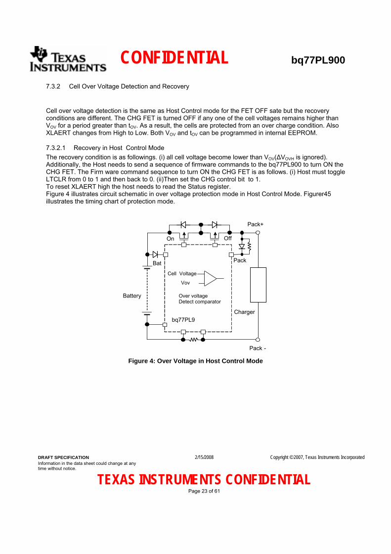
7.3.2 Cell Over Voltage Detection and Recovery
Cell over voltage detection is the same as Host Control mode for the FET OFF sate but the recovery conditions are different. The CHG FET is turned OFF if any one of the cell voltages remains higher than VOV for a period greater than tOV. As a result, the cells are protected from an over charge condition. Also XLAERT changes from High to Low. Both VOV and tOV can be programmed in internal EEPROM.
7.3.2.1 Recovery in Host Control Mode The recovery condition is as followings. (i) all cell voltage become lower than VOV(∆VOVH is ignored). Additionally, the Host needs to send a sequence of firmware commands to the bq77PL900 to turn ON the CHG FET. The Firm ware command sequence to turn ON the CHG FET is as follows. (i) Host must toggle LTCLR from 0 to 1 and then back to 0. (ii)Then set the CHG control bit to 1. To reset XLAERT high the host needs to read the Status register. Figure 4 illustrates circuit schematic in over voltage protection mode in Host Control Mode. Figurer45 illustrates the timing chart of protection mode.
Figure 4: Over Voltage in Host Control Mode
Pack
bq77PL9
Pack+
Pack -
Charger
On Off
Over voltage Detect comparator Battery
Bat
Vov
Cell Voltage

CONFIDENTIAL bq77PL900
DRAFT SPECIFICATION Information in the data sheet could change at any time without notice.
2/15/2008 Copyright © 2007, Texas Instruments Incorporated
TEXAS INSTRUMENTS CONFIDENTIAL Page 24 of 61
Figure 5: OV and OV recovery timing in Host Control Mode
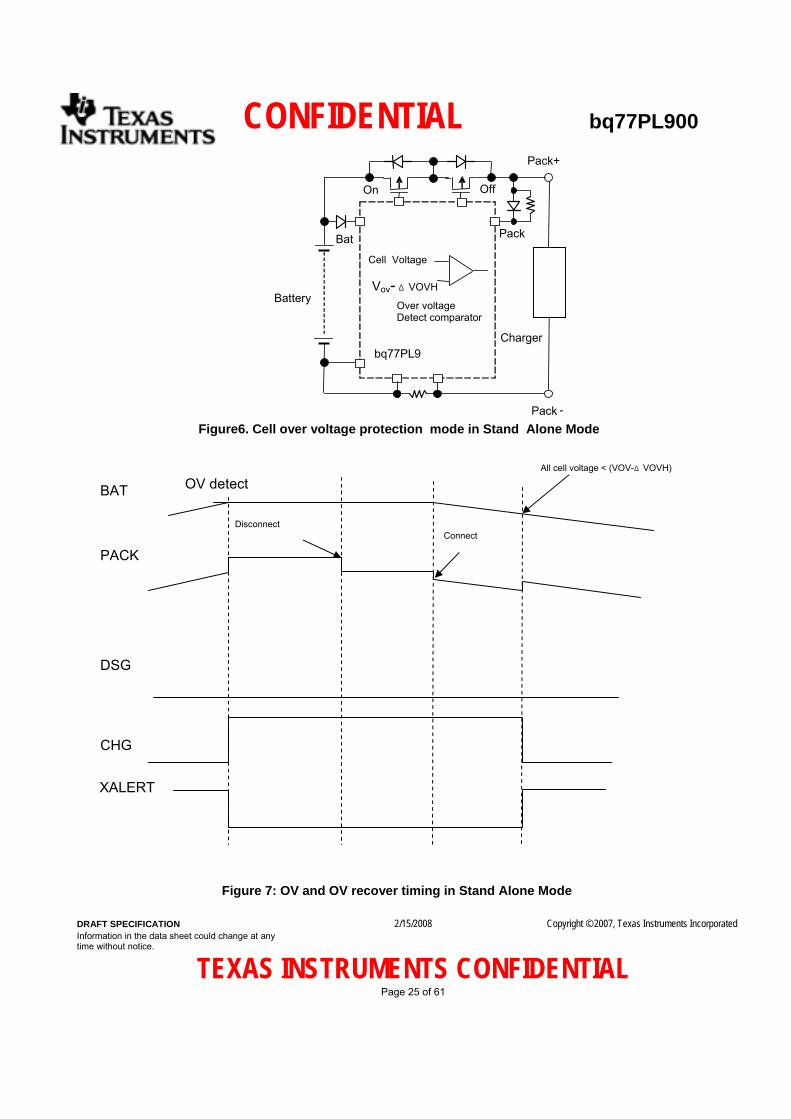
7.3.2.2 Recovery in Stand Alone Mode The recovery condition occurs when all cell voltage becomes lower than (VOV-∆VOVH). Figure 6 illustrates circuit schematic in over voltage protection mode in Stand Alone Mode. Figure 7 illustrates the timing chart of protection mode.
Disconnect
BAT
PACK
DSG
CHG
OV detect All cell voltage <VOV
Connect
Host turns on CHG
XALERT Host reads SATUS
CONFIDENTIAL bq77PL900
DRAFT SPECIFICATION Information in the data sheet could change at any time without notice.
2/15/2008 Copyright © 2007, Texas Instruments Incorporated
TEXAS INSTRUMENTS CONFIDENTIAL Page 25 of 61
Figure6. Cell over voltage protection mode in Stand Alone Mode
Figure 7: OV and OV recover timing in Stand Alone Mode
Pack
bq77PL9
Pack+
Pack -
Charger
On Off
Battery
Bat
Over voltage Detect comparator
Vov- ΔVOVH
Cell Voltage
Disconnect
BAT
PACK
DSG
CHG
OV detect All cell voltage < (VOV-ΔVOVH)
Connect
XALERT

CONFIDENTIAL bq77PL900
DRAFT SPECIFICATION Information in the data sheet could change at any time without notice.
2/15/2008 Copyright © 2007, Texas Instruments Incorporated
TEXAS INSTRUMENTS CONFIDENTIAL Page 26 of 61
7.3.3 Cell Under Voltage Detection and Recovery When any one of the cell voltages falls below VUV, for a period of tUV, bq77PL900 enters under voltage mode. At this time the DSG FET is turned OFF and XALERT driven low. Both VUV and tUV can be programmed in internal EEPROM.
Load
Pack
bq29500
Pack+
Pack-
Off On
Under voltage Detect comparator
Charge CurrentDetect comparator Load
Battery
Bat
Load
Pack
bq29500
Pack+
Pack-
Off On
Under voltage Detect comparator
Charge CurrentDetect comparator Load
Battery
Bat
Figure 8: Cell under voltage protection mode at Host Control Mode
and Stand Alone Mode(attaching a Charger)

CONFIDENTIAL bq77PL900
DRAFT SPECIFICATION Information in the data sheet could change at any time without notice.
2/15/2008 Copyright © 2007, Texas Instruments Incorporated
TEXAS INSTRUMENTS CONFIDENTIAL Page 27 of 61
7.3.3.1 In Host Control Mode Cell under voltage protection recovery conditions are when (i) all cell voltage become higher than (VUV+∆VUVH) or (ii) all cell voltages are higher than VUV AND a charger is connected between PACK+ and PACK- noting that PACK+ voltage must be higher than BAT due to the diode forward voltage. The bq77PL900 monitors the difference of voltage between PACK+ and BAT voltage. When a difference higher than 0.4V(typ), it is interpreted that a charger has been connected. Figure 8 illustrates circuit schematic in under voltage protection mode. In some applications, it is required to not turn OFF the DSG FET suddenly. In these cases, by setting UVLEVLE [UVFET_DIS] =1, only XALERT is driven low in response to entering an under voltage condition. The host can turn OFF the DSG FET to protect under voltage condition. When the bq77PL900 recovery condition is satisfied, the host needs to send a sequence of firmware commands to the bq77PL900.The firmware command sequence to turn ON the DSG FET is as following. (i)Host must toggle LTCLR from 0 to 1 and back to 0, (ii)Then set the DSG ON bit to 1. Then Host can then read the status register to reset XALERT high. Figurer9 and Figure10 illustrate the timing chart of protection mode.
Figure 9: UV and UV recovery timing Host Control Mode (UVFET_DIS=0)
All cell voltage > (VUV +ΔVUVH) Or [All cell voltage > VUV] and [detecting (PACK+)- VBAT> 0.1V]
Connect a
BAT
PACK
DSG
CHG
XALERT
UV detection
Host turns on DSG
Host read status

CONFIDENTIAL bq77PL900
DRAFT SPECIFICATION Information in the data sheet could change at any time without notice.
2/15/2008 Copyright © 2007, Texas Instruments Incorporated
TEXAS INSTRUMENTS CONFIDENTIAL Page 28 of 61
Connect a Charger
BAT
PACK
DSG
CHG
XALERT
All cell voltage > (VUV +ΔVUVH)OrAll cell voltage > VUVand detecting (PACK+)- VBAT> 0.1V
UV detection
Host turns on DSG FET
Host read status register
Host turns off DSG FET
DSG not turning off
Connect a Charger
BAT
PACK
DSG
CHG
XALERT
All cell voltage > (VUV +ΔVUVH)OrAll cell voltage > VUVand detecting (PACK+)- VBAT> 0.1V
UV detection
Host turns on DSG FET
Host read status register
Host turns off DSG FET
DSG not turning off
Figure 10: UV and UV recovery timing Host Control Mode (UVFET_DIS=1)

CONFIDENTIAL bq77PL900
DRAFT SPECIFICATION Information in the data sheet could change at any time without notice.
2/15/2008 Copyright © 2007, Texas Instruments Incorporated
TEXAS INSTRUMENTS CONFIDENTIAL Page 29 of 61
7.3.3.2 In Stand Alone Mode On detection on entry to under voltage mode the bq77PL900 moves to the SHUTDOWN power mode. When a charger is attached, the bq77PL900 wakes up from shutdown mode. If cell voltages are lower than the under voltage condition, the DSG FET is turned OFF and XALERT driven low. During periods when a charger is attached the bq77PL900 never changes to shutdown mode. When the under voltage recovery condition is satisfied, the DSG FET turns ON and XLAERT is reset high.
Figure 11: UV and UV recovery in Stand Alone Mode
Connect
BAT
PACK
DSG
CHG
REG1 /REG2
UV detect
All cell voltage > (VUV +ΔVUVH) Or [All cell voltage > VUV] and [detecting (PACK+)- VBAT> 0.1V]
Change to shut down
Wake up
UV

CONFIDENTIAL bq77PL900
DRAFT SPECIFICATION Information in the data sheet could change at any time without notice.
2/15/2008 Copyright © 2007, Texas Instruments Incorporated
TEXAS INSTRUMENTS CONFIDENTIAL Page 30 of 61
7.3.4 Over Current in Discharge (OCD) Detection The over current in discharge detection feature detects abnormal currents in the discharge direction via measuring the voltage across the sense resistor (VOCD) and is used to protect the pass FETs, cells and any other inline components from abnormal discharge current conditions. The detection circuit also incorporates a blanking delay period (tOCD) before turning OFF the pass FETs. Both VOCD and tOCD can be programmed in internal EEPROM.
7.3.5 Short Circuit in Discharge (SCD) Detection The short circuit in discharge detections feature detects severe discharge current via measuring the voltage across the sense resistor (VSCD) and is used to protect the pass FETs, cells and any other inline components from severe current conditions. The detection circuit also incorporates a blanking delay period (tSCD) before turning OFF the pass FETs. Both VSCD and tSCD can be programmed in internal EEPROM.
7.3.6 Over Current in Discharge and Short Circuit in Discharge Recovery In Host control mode, the Host needs to send a sequence of firmware commands to the bq77PL900. The firmware command sequence to turn ON the DSG and CHG FETs is as follows. (i)Host must toggle LTCLR from 0 to 1 and back to 0, (ii)Then set 1 the DSG and CHG control bits to 1.To reset XALERT high the STATUS register needs to be read In Stand Alone Mode, the bq77PL900 has two methods to recover from Over Current and Short Circuit conditions by setting SOR bit of OCD_CFG.
SOR = 0, Recover comparator is active after 12.8sec. An internal comparator monitors the PACK+ voltage and when the PACK+ voltage reaches VRECSC, the over current in discharge recovers. When the bq77PL900 detects attaching a charger, the DSG and CHG FETs turn ON and XLAERT reset High.
SOR = 1, after 12.8sec, the bq77PL900 automatically recovers from OC and SC. The DSG and CHG FETs turn ON and XLAERT is reset high. If the OC or SC condition is still present, OC and SC will be detected again and the recovery/detection cycle continues until the fault is removed.
bq29500
Pack+
Pack -
Off Off
LoadOL/SC releaseComparator
Pack
Battery
Bat
bq29500
Pack+
Pack -
Off Off
LoadOL/SC releaseComparator
Pack
Battery
Bat
Figure 12: Over Current and Short Circuit protection modes

CONFIDENTIAL bq77PL900
DRAFT SPECIFICATION Information in the data sheet could change at any time without notice.
2/15/2008 Copyright © 2007, Texas Instruments Incorporated
TEXAS INSTRUMENTS CONFIDENTIAL Page 31 of 61
Table 3: Detection and Recovery Condition Summary (Stand Alone Mode)
CELL OVER VOLTAGE CELL UNDER VOLTAGE OVER CURRENT IN DISCHARGE
SHORT CIRCUIT IN DISCHARGE
Detection condition Any Cell Voltage > VOV Any Cell Voltage < VUV (VSRP - VSRN) > VOCD (VSRP - VSRN) > VSCD
CHG FET ON → OFF ON ON →OFF ON →OFF
DSG FET ON ON →OFF ON →OFF ON →OFF
Recovery Condition 1
All cell voltage < (VOV - ∆VOVH)
All cell voltage > (VUV +∆VUVH)
SOR=0: Attach a charger SOR=1:OC condition is
released
SOR=0: Attach a charger SOR=1: SC condition is
released
Recovery Condition 2
All cell voltage > VUV AND
PACK+ - VBAT >0.1V
CHG FET OFF →ON ON OFF → ON OFF → ON
DSG FET ON OFF →ON OFF →ON OFF →ON
Table 4: Detection and Recovery Condition Summary (Host Control Mode)
CELL OVER VOLTAGE CELL UNDER VOLTAGE OVER CURRENT IN DISCHARGE
SHORT CIRCUIT IN DISCHARGE
Detection condition Any Cell Voltage > VOV Any Cell Voltage < VUV (VSRP - VSRN) > VOCD (VSRP - VSRN) > VSCD
CHG FET ON → OFF ON ON →OFF ON →OFF
DSG FET ON ON →OFF ON →OFF ON →OFF
Recovery Condition 1
All cell voltage < VOV
(ignore the hysteresis) All cell voltage >
(VUV +∆VUVH) None None
Recovery Condition 2
All cell voltage > VUV AND
VPACK- VBAT >0.1V
CHG FET(1) OFF →ON ON OFF → ON OFF → ON
DSG FET(1) On OFF →ON OFF →ON OFF →ON
Notes 1: Host is required to set and clear LTCLR, then turn on the FETs.

CONFIDENTIAL bq77PL900
DRAFT SPECIFICATION Information in the data sheet could change at any time without notice.
2/15/2008 Copyright © 2007, Texas Instruments Incorporated
TEXAS INSTRUMENTS CONFIDENTIAL Page 32 of 61
7.4 Low Drop Out Regulators (REG1 and REG2) The bq77PL900 has two Low Drop Out (LDO) regulators that provides power to both internal and external circuitry. The inputs for these regulators can be derived from the PACK or BAT terminals (see Initialization for further details). The output of REG1 is typically 5.0 V with the minimum output capacitance for stable operation with 2.2µF and is also internally current limited. During normal operation, the regulator limits output current to typically 25mA. The output of REG2 is typically 3.3 V with the minimum output capacitance for stable operation with 2.2µF and is also internally current limited. Until the internal regulator circuit is correctly powered, the DSG and CHG FETs are driven OFF.
7.5 Initialization From a shutdown situation the bq77PL900 requires a voltage greater that the Start Up Voltage (VSTARTUP) applied to the PACK pin to enable its integrated regulator and provide the regulators power source. Once the REG1 and REG2 outputs become stable, the power source of the regulator is switched to BAT. After the regulators have started they will then continue to operate through the BAT input. If the BAT input is below the minimum operating range then the bq77PL900 will not operate until the supply to the PACK input is applied. If the voltage at REG2 falls the internal circuit will turn off the CHG and DSG FETs and disable all controllable functions including the REG1, REG2 and TOUT outputs.
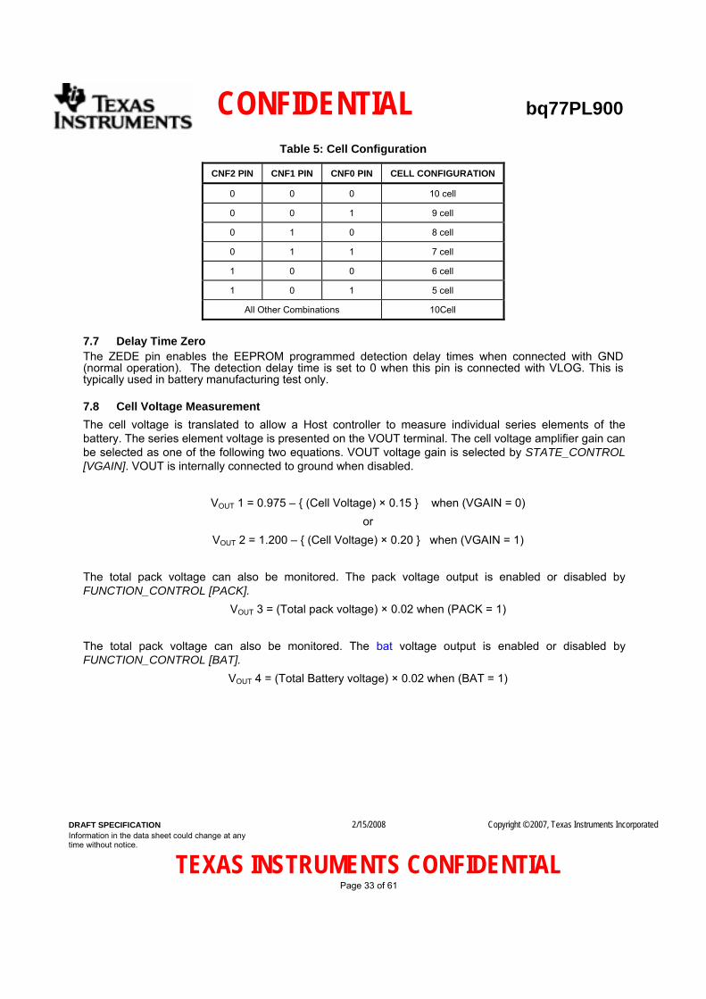
7.6 5 to 10 Series Cell Configuration Unused cell inputs are required to be shorted to the upper most voltage connected terminal. For example, in a 5-cell configuration VC1 to VC5 are shorted to VC6. In a 9-cell configuration VC1 is shorted to VC2. CNF0, CNF1, CNF2 pins should be connected to VLOG = logic 1 (through 10kΩ resistance) or GND = logic 0 (directly) according to the desired cell configuration as seen below.
CONFIDENTIAL bq77PL900
DRAFT SPECIFICATION Information in the data sheet could change at any time without notice.
2/15/2008 Copyright © 2007, Texas Instruments Incorporated
TEXAS INSTRUMENTS CONFIDENTIAL Page 33 of 61
Table 5: Cell Configuration
CNF2 PIN CNF1 PIN CNF0 PIN CELL CONFIGURATION
0 0 0 10 cell
0 0 1 9 cell
0 1 0 8 cell
0 1 1 7 cell
1 0 0 6 cell
1 0 1 5 cell
All Other Combinations 10Cell
7.7 Delay Time Zero The ZEDE pin enables the EEPROM programmed detection delay times when connected with GND (normal operation). The detection delay time is set to 0 when this pin is connected with VLOG. This is typically used in battery manufacturing test only.
7.8 Cell Voltage Measurement The cell voltage is translated to allow a Host controller to measure individual series elements of the battery. The series element voltage is presented on the VOUT terminal. The cell voltage amplifier gain can be selected as one of the following two equations. VOUT voltage gain is selected by STATE_CONTROL [VGAIN]. VOUT is internally connected to ground when disabled.
VOUT 1 = 0.975 – (Cell Voltage) × 0.15 when (VGAIN = 0) or
VOUT 2 = 1.200 – (Cell Voltage) × 0.20 when (VGAIN = 1)
The total pack voltage can also be monitored. The pack voltage output is enabled or disabled by FUNCTION_CONTROL [PACK].
VOUT 3 = (Total pack voltage) × 0.02 when (PACK = 1)
The total pack voltage can also be monitored. The bat voltage output is enabled or disabled by FUNCTION_CONTROL [BAT].
VOUT 4 = (Total Battery voltage) × 0.02 when (BAT = 1)

CONFIDENTIAL bq77PL900
DRAFT SPECIFICATION Information in the data sheet could change at any time without notice.
2/15/2008 Copyright © 2007, Texas Instruments Incorporated
TEXAS INSTRUMENTS CONFIDENTIAL Page 34 of 61
7.9 Cell Voltage Measurement Calibration The bq77PL900 Cell Voltage monitor consists of a S/H (sample and hold) circuit and differential amplifier.
Figure 13: Cell Voltage Monitoring Circuit To calibrate the VCELL output, it needs to measure a 2.5v signal, but 2.5V is beyond the ADC input range of most Analog to Digital converters used in these applications. The bq77PL900 is designed to measure the 2.5V through differential amplifier first which is where the calibration step starts from.
Figure 14: Calibration Method
VOUT
0V VC(n+1)-VCn
Step5 Vout(VREF_m)
Step6 Vout(2.5V)
VREF_m(0.975V or 1.2V)
VOUT
0V Differential Amp Input
Step1 Vdout(0V)
Step2 VREF_mStep2 VREF_m
Step3 Vdout(VREF_m)
Step4 Vdout(2.5V)
KdACT
VREF_m(0.975V or 1.2V)
Calculate VREF_2.5V from Step 1-4
VREF_2.5V VREF_2.5V
VOUT
0V VC(n+1)-VCn
Step5 Vout(VREF_m)
Step6 Vout(2.5V)
VREF_m(0.975V or 1.2V)
VOUT
0V Differential Amp Input
Step1 Vdout(0V)
Step2 VREF_mStep2 VREF_m
Step3 Vdout(VREF_m)
Step4 Vdout(2.5V)
KdACT
VREF_m(0.975V or 1.2V)
Calculate VREF_2.5V from Step 1-4
VREF_2.5V VREF_2.5V
VOUT
VREF=0.975V or 1.2V
Sample and Hold Circuit
Differential Amp Circuit
VC11
VC10
VC9
VC8
REF=2.5V
Calibration
VOUT
VREF=0.975V or 1.2V
Sample and Hold Circuit
Differential Amp Circuit
VC11
VC10
VC9
VC8
REF=2.5V
Calibration
CONFIDENTIAL bq77PL900
DRAFT SPECIFICATION Information in the data sheet could change at any time without notice.
2/15/2008 Copyright © 2007, Texas Instruments Incorporated
TEXAS INSTRUMENTS CONFIDENTIAL Page 35 of 61
7.9.1 Step 1 Set CAL2=0,CAL1=0, CAL0=1, CELL[4:1]=0, VAEN=1 Measure the output voltage of differential amp at 0V input( both input of differential amp are connected GND). The output voltage includes the offset and represented by
VdOUT(0V) = measured output voltage of differential amplifier at 0V input (This value includes an offset voltage(VOS )and a reference voltage)
7.9.2 Step 2 Set CAL2=0, CAL1=1, CAL0=1, VAEN=1 VREF is trimmed to 0.975V or 1.2V within +-2%. Then measure internal reference voltage VREF from VOUT directly
VREF_m = measured reference voltage(0.975V or 1.2V)
7.9.3 Step 3 Set CAL2=0, CAL1=1, CAL0=0, CELL[4:1]=0, VAEN=1 Measure scaled REF voltage through differential amp. VdOUT(VREF_m) = The output voltage includes the scale factor error and offset =VREF+(1+K)* VOS – K * VREF = VREF_m + (1 + KdACT) * VOS – KdACT * VREF_m
Where VREF_m+ (1 + KdACT) * VOS =VdOUT(0V)
KdACT =( VdOUT(0V) – VdOUT(VREF_m)) / VREF_m =(measured value @step1 – measured value@step3)/ measured value@step2
Calibrated differential voltage is calculated by: Vdout = VREF+(1+K)* VOS – K * Vdin
= VdOUT(0V) – KdACT * Vdin Where Vdin= input voltage of differential amp
7.9.4 Step 4 Set CAL2=1, CAL1=0, CAL0=0, CELL[4:1]=0, VAEN=1 Measure scaled REF(2.5V) though differential amp, In case of bq-GG, it can not measure 2.5V direct, because of it’s ADC input voltage is 1.0V. So to measure the 2.5V internal reference voltage, using differential amp is a method to turn down the measurement value. Vdout(2.5V) = measured differential amp output voltage at 2.5V input Already, differential amp calibration was done by step1,2 and 3. So VREF_2.5V is presented by VREF_2.5V= VdOUT(0V)- Vdout(2.5V)/ KdACT
7.9.5 Step 5 Set CAL2=1,CAL1=0, CAL0=1, CELL2=0, CELL1=0, VAEN=1

CONFIDENTIAL bq77PL900
DRAFT SPECIFICATION Information in the data sheet could change at any time without notice.
2/15/2008 Copyright © 2007, Texas Instruments Incorporated
TEXAS INSTRUMENTS CONFIDENTIAL Page 36 of 61
Vout(0.975V or 1.2V) = Measure scaled REF(0.975V or 1.2V) output voltage S/H and differential amplifier.
7.9.6 Step 6 Set CAL2=1, CAL1=1, CAL0=0, CELL[4:1]=0, VAEN=1 Vout(2.5V) = Measure scaled REF(2.5V) output voltage S/H and differential amp. Scale factor KACT =( VOUT(2.5V) – VOUT(0.975Vor1.2V) /( VREF_2.5V-VREF_m) Vout(0V)= VOUT(2.5V) – KACT *VREF_2.5V
Or Vout(0V)= VOUT(0.975Vor1.2V) – KACT *VREF_m
Cell voltage is calculated by below VCn – VC(n+1) = Vout(0V) – VOUT / KACT
7.10 Current Monitor Discharge and charge current is translated to allow a Host controller to accurately measure current which can then be used for additional safety features or calculating the remaining capacity of the battery. The sense resistor voltage is converted per the equation below. The typical offset voltage is VCELL_OFF(1.20V typical) although can be presented on the IOUT pin for measurement if required. The output voltage increases when current is positive (discharging) and decreases when current is negative (charging).
VCURR = 1.20 + (IPACK × RSENSE) × (IGAIN) Where
State_Contorl [IGAIN] = 1 then IGAIN = 50 State_Contorl [IGAIN] = 0 then IGAIN = 10
The current monitor amplifier can present the offset voltage as shown in table 6. The IOUT pin is enabled or disabled by FUNCTION_CONTROL [IACAL, IAEN] and has a default state of OFF. IOUT is internally connected to ground when disabled
Table 6: IACAL and IAEN Configuration
IACAL IAEN CONDITION
0 1 NORMAL
1 1 OFFSET
X 0 OFF
7.11 Cell Balance Control The integrated cell balance FETs allow a bypass path to be enabled for any one series element. The purpose of this bypass path is to reduce the current into any one cell during charging to bring the series elements to the same voltage. Series resistors placed between the input pins and the positive series element nodes limits the bypass current value. Series input resistors between 500Ω and 1kΩ are recommended for effective cell balancing.

CONFIDENTIAL bq77PL900
DRAFT SPECIFICATION Information in the data sheet could change at any time without notice.
2/15/2008 Copyright © 2007, Texas Instruments Incorporated
TEXAS INSTRUMENTS CONFIDENTIAL Page 37 of 61
In Host Control Mode, individual series element selection is made via CELL_BALANCE [CBAL1, CBAL2, CBAL3, CBAL4, CBAL5, CBAL6, CBAL7, CBAL8] and FUNCTION_CONTROL [ CBAL9, CBAL10]. In Stand Alone mode, cell balancing works as shown in the figure below. When a certain cell (Cell A) voltage reaches cell over voltage, the battery charging stops and then cell balance starts working at ta. The Cell A voltage decreases by the bypass current until the voltage reaches (VOV -∆VOVH). Cell B voltage doesn’t change during the period because cell balancing works only for the cell that reached VOV. At tb, battery charging starts again. Cell A and Cell B have been charged in this period until Cell A voltage reaches VOV again. The voltage difference between Cell A and Cell B becomes smaller when the bq77PL900 repeats the above cycle. The bq77PL900 stops cell balance when cell over voltage protection has released. bq77PL900 is designed to prevent cell balancing on adjacent cells or on every other cells. For example, if cell over voltage happened to Cell 8 and Cell 7 (Cell7 is next to Cell8 and higher) and Cell3( Cell3 is not next to Cell8 and Cell7), cell balance starts for Cell8 and Cell3 at first. When Cell8 voltage is back to normal voltage, cell balance starts for Cell7. While the bq77PL900 monitors the over voltage and under voltage, Cell balance automatically will be turn off. This configuration is supported for both modes (Host control and Stand Alone mode).
Figure 15: Cell Balancing timing chart (Automatic)
7.12 Thermistor Drive Circuit (TOUT), Thermistor Input (TIN) The TOUT pin is powered by REG2 and can be enabled via FUNCTION_CONTROL [TOUT] to drive an external thermistor and is default OFF. A 10kΩ 25ºC NTC (eg: Semitec 103AT) thermistor is typical. The maximum output impedance is 100Ω. The bq77PL900 monitors the battery temperature as shown below. A voltage divided by the NTC thermistor and reference resistor is connected to TIN. The bq77PL900 compares the TIN voltage with the internal reference voltage (0.975V) and when VTIN < VREF the bq77PL900 turns OFF the CHG and DSG FETs and sets STATUS [OVTEMP]. In Host Control Mode, the host should enable and disable the TOUT.
Vov-∆Vovh
Vdiffa
Cell A
Cell B
Vdiffb Vov
ta tb tc td te tf

CONFIDENTIAL bq77PL900
DRAFT SPECIFICATION Information in the data sheet could change at any time without notice.
2/15/2008 Copyright © 2007, Texas Instruments Incorporated
TEXAS INSTRUMENTS CONFIDENTIAL Page 38 of 61
Figure 16: Temperature Monitoring Circuit
7.13 General Purpose Open Drain Drive (GPOD) The GPOD output is enabled or disabled by OUTPUT_CONTROL [GPOD] and has a default state of OFF. In Stand Alone Mode, this pin is used for driving the 0V/Pre-charge FET for zero voltage battery charging by OCD_CFG [ZVC]=1
7.14 Alerting the Host (XALERT) In both modes the XALERT pin is available and is driven low when faults are detected. The method to clear the XALERT pin is different between Stand Alone Mode and Host Control Mode. In Stand Alone Mode, XLAERT is cleared when all of faults are cleared. In Host Control Mode, the host has to toggle (from “0”, set to “1” then reset to “0”) OUTPUT_CONTROL [LTCLR] and then read the STATUS register.
TOUT
CTHERM
RTHERM
VREF
TIN
3.3V

CONFIDENTIAL bq77PL900
DRAFT SPECIFICATION Information in the data sheet could change at any time without notice.
2/15/2008 Copyright © 2007, Texas Instruments Incorporated
TEXAS INSTRUMENTS CONFIDENTIAL Page 39 of 61
7.15 Alerting the Host (LTCLR) In Host Control Mode, when a protection fault occurs, the state is latched. The fault flag is un latched by toggling (from “0”, set to “1” then reset to “0”) OUTPUT_CONTROL [LTCLR]. The OCD, SCD, OV and UV bits are unlatched by this function. Now the FETs can be controlled by programming the OUTPUT_CONTROL register and the XALERT output can be cleared by reading the STATUS register. During detecting an over voltage or under voltage faults, LTCTR changes are ignored. After a period of 1ms, it needs to send a LTCLR command.
Figure 17: LTCLR and XLAERT Clear Timing (Host Control Mode )
7.16 POR The XRST open drain output pin will be triggered on activation of the VREG1 or VREG2 output. This holds the Host controller in reset for tRST allowing the VVREG1 or VVREG2 to stabilize before the host controller is released from reset. The XRST output and monitoring voltage is supplied by the source of VLOG. When VLOG is connected to VREG1, the XRST output level is VVREG1 and monitors activation of the VREG1. When VLOG is connected to VREG2, the XRST output level is VVREG2 and monitors activation of the VREG2. When VVREG1 or VVREG2 voltage is below the output specifications, XRST will be active low(0.8x VLOG). When VBAT is below 7.0V, VREG1 and VREG2 will stop, then XRST will go low. If a Host has a problem with a sudden Reset signal, it is recommended monitoring the Battery voltage to avoid it, eg: burnout detection.
tRST
VREGTH+
VREGTH-
REG Output
XRST Output
VLOG
Figure 18: XRST Timing Chart – Power Up and Power down
FET Control Accessby Host
LTCLR Bit
Fault Flag Set
XALERT Output
Fault TimeoutExpired
STATUS RegisterRead

CONFIDENTIAL bq77PL900
DRAFT SPECIFICATION Information in the data sheet could change at any time without notice.
2/15/2008 Copyright © 2007, Texas Instruments Incorporated
TEXAS INSTRUMENTS CONFIDENTIAL Page 40 of 61
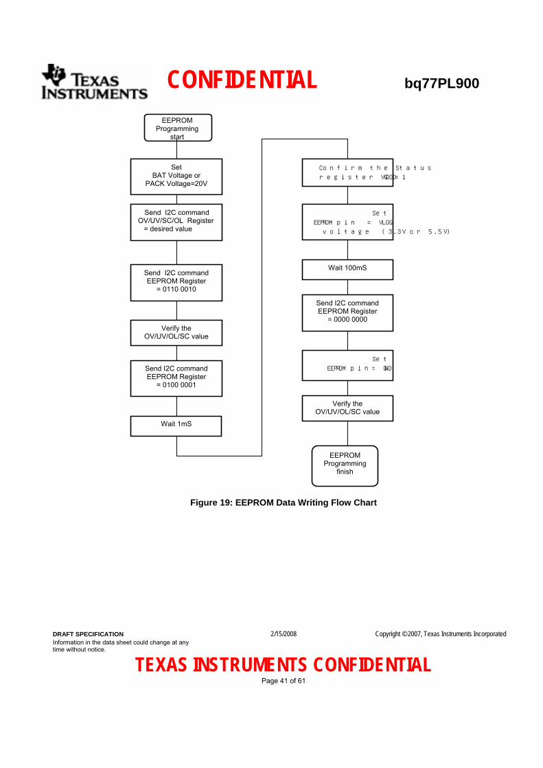
7.17 EEPROM Write Sequence The bq77PL900 has integrated configuration EEPROM for OV, UV, OCD and SCD thresholds and delays. The appropriate configuration data is programmed to the configuration registers and then 0xe2 is sent to the EEPROM register to enable the programming supply voltage. By driving the EEPROM pin (set high and then low), the data is written to the EEPROM. When Supplying BAT, care should be taken not to exceed VCn – VC(n+1), (n=1 to 10 ) >5.0V. If BAT and VC1 is connected on board, we recommend that all of cell balance FETs be ON where each input voltage is divided with internal cell balance ON resistance. The recommended voltage at BAT or PACK for EEPROM writing is 20V. When Supplying VBAT, care is needed to ensure VBAT does not exceed the “VCn – VC(n+1), (n=1 to 10 ) absolute max voltage”. If BAT and VC1 are connected on board, we recommend supplying 7.5V to activate the bq77PL900 and turns ON all of cell balance FETs. Then increase the power supply up to 20V. By this method, each input Voltage is divided with internal cell balance ON resistance.
CONFIDENTIAL bq77PL900
DRAFT SPECIFICATION Information in the data sheet could change at any time without notice.
2/15/2008 Copyright © 2007, Texas Instruments Incorporated
TEXAS INSTRUMENTS CONFIDENTIAL Page 41 of 61
Figure 19: EEPROM Data Writing Flow Chart
EEPROM
Programming start
Send I2C command EEPROM Register
= 0110 0010
Send I2C command OV/UV/SC/OL Register = desired value
Confirm the Status
register VGOOD=1
Verify the
OV/UV/OL/SC value
Set BAT Voltage or
PACK Voltage=20V
Send I2C command EEPROM Register
= 0100 0001
Wait 1mS
Wait 100mS
Verify the OV/UV/OL/SC value
Send I2C command EEPROM Register
= 0000 0000
Set
EEPROM pin= GND
Set
EEPROM pin = VLOG
voltage (3.3V or 5.5V)
EEPROM Programming
finish

CONFIDENTIAL bq77PL900
DRAFT SPECIFICATION Information in the data sheet could change at any time without notice.
2/15/2008 Copyright © 2007, Texas Instruments Incorporated
TEXAS INSTRUMENTS CONFIDENTIAL Page 42 of 61
7.18 Power Modes The bq77PL900 has two power modes, Normal and shutdown. The following table outlines the operational functions during two power modes.
Table 7: Power Modes
POWER MODE
TO ENTER NORMAL MODE MODE DESCRIPTION
Normal The battery is in normal operation with protection, power management and battery monitoring functions available and operating. The supply current of this mode varies as the Host can enable and disable various features.
Shutdown Add supply at the VPACK < VWAKE
When under voltage is detected in Stand Alone Mode, or Shutdown command at Host Control Mode , The bq77PL900 goes shut down, All outputs and interfaces are OFF and memory is not valid.
7.18.1 Shutdown Mode In Host Control Mode the bq77PL900 enters shutdown mode when it receives the shutdown command, STATE_CONTROL [SHDN] set. First the DSG FET will be turned OFF and then after the Pack voltage goes to 0V, the bq77PL900 enters to shut down mode which stops all functions of bq77PL900. In Stand Alone Mode the bq77PL900 enters shutdown when the battery voltage falls, and UV is detected. It turns the DSG FET OFF and after the Pack voltage goes to 0V, the bq77PL900 enters to shut down mode which stops all functions.
7.18.2 Exit From Shutdown If a voltage greater than VSTARTUP is applied to the PACK pin then the bq77PL900 will exit from shutdown and enter to normal mode.
7.19 Parity check The bq77PL900 uses EEPROM for storage of protection thresholds and delay times etc… The EEPROM is also used to store internal trimming data. For safety reasons, the bq77PL900 is uses a column parity error checking scheme. If the column parity bit is changed from the written then OUT_CONTROL [PFALT] is set to 1 and XALERT driven low. In Stand alone mode, both DSG and CHG outputs are driven high turning OFF the DSG and CHG FETs. And GPOD output is turned off, too. In Host Control Mode, only OUT_CONTROL [PFALT] and XALERT output are changed, so allowing the micro processor host to control bq77PL900’s operation.
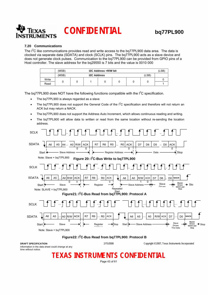
CONFIDENTIAL bq77PL900
DRAFT SPECIFICATION Information in the data sheet could change at any time without notice.
2/15/2008 Copyright © 2007, Texas Instruments Incorporated
TEXAS INSTRUMENTS CONFIDENTIAL Page 43 of 61
7.20 Communications The I2C like communications provides read and write access to the bq77PL900 data area. The data is clocked via separate data (SDATA) and clock (SCLK) pins. The bq77PL900 acts as a slave device and does not generate clock pulses. Communication to the bq77PL900 can be provided from GPIO pins of a Host controller. The slave address for the bq29550 is 7 bits and the value is 0010 000
(MSB) I2C Address +R/W bit (LSB) (MSB) I2C Address (LSB)
Write 0 Read
0 0 1 0 0 0 0 1
The bq77PL900 does NOT have the following functions compatible with the I2C specification.
• The bq77PL900 is always regarded as a slave
• The bq77PL900 does not support the General Code of the I2C specification and therefore will not return an ACK but may return a NACK.
• The bq77PL900 does not support the Address Auto Increment, which allows continuous reading and writing.
• The bq77PL900 will allow data to written or read from the same location without re-sending the location address.
Figure 20: I2C-Bus Write to bq77PL900
Figure21: I2C-Bus Read from bq77PL900: Protocol A
Figure22: I2C-Bus Read from bq77PL900: Protocol B
A5
… … …
… … …
SCLK
SDATA
Slave Address Register Address Data StopStart
Note: Slave = bq77PL900
A6 ACKR/W A0 A4 R5 R6 R7 R0 D7 ACK D6 D5 D0 ACK0 0 0 0
Note: SLAVE = bq77PL900
A5
… …
…… …
…SCLK
SDATA
Slave Register Add
Slave Address StoStart
A6 ACK R/W A0 R6R7 R0 A6 ACK A0 R/W ACK D7 0 0 0 1 0
…
D6 D0 NACK
RepeatedStart
Slave Drives
Master Drives
NACK and Stop
A5
… …
…… …
…SCLK
SDATA
Slave Register Address
Slave Address StopStart
Note: Slave = bq77PL900
A6 ACK R/W A0 R6R7 R0 A6 ACK A0 R/W ACK D7 0
…
D0 NACK
Slave Drives
The Data
Master Drives
NACK and Stop
A5 …
Stop Start

CONFIDENTIAL bq77PL900
DRAFT SPECIFICATION Information in the data sheet could change at any time without notice.
2/15/2008 Copyright © 2007, Texas Instruments Incorporated
TEXAS INSTRUMENTS CONFIDENTIAL Page 44 of 61
7.21 Register Set The bq77PL900 has 12 addressable registers. These registers provide status, control, and configuration information for the battery protection system.
Table 8: Register Descriptions
Table 9: Register Map
NAME I2C
ADDR B7 B6 B5 B4 B3 B2 B1 B0
STATUS 0x00 CHG DSG VGOOD OVTEMP UV OV OCD SCD
OUTPUT_CONTROL 0x01 FS PFALT 0 0 GPOD CHG DSG LTCLR
STATE_CONTROL 0x02 IGAIN VGAIN 0 0 0 0 HOST SHDN
FUNCTION_CONTROL
(Cell(9,10)Balance Register) 0x03 CBAL10 CBAL9 TOUT BAT PACK IACAL IAEN VAEN
CELL BALANCE 0x04 CBAL8 CBAL7 CBAL6 CBAL5 CBAL4 CBAL3 CBAL2 CBAL1
CELL _SEL 0x05 0 CAL2 CAL1 CAL0 CELL4 CELL3 CELL2 CELL1
OV_CFG 0x06 OVD2 OVD1 OVD0 OVH1 OVH0 OV2 OV1 OV0
UV_CFG 0x07 0 UVFET_DIS
UVH1 UVH0 UV3 UV2 UV1 UV0
OCV&UV_DELAY 0x08 UVD3 UVD2 UVD1 UVD0 OCD3 OCD2 OCD1 OCD0
OCD_CFG 0x09 CBEN ZVC SOR OCDD4 OCDD3 OCDD2 OCDD1 OCDD0
SCD_CFG 0x0a SCDD3 SCDD2 SCDD1 SCDD0 SCD3 SCD2 SCD1 SCD0
NAME Test Pin ADD
R MEMORY
TYPE R/W DESCRIPTION
STATUS X 0x00 Read R Status register
OUTPUT_CONTROL X 0x01 RAM R/W Output pin control from system Host Control Mode and external pin
status
STATE_CONTROL X 0x02 RAM R/W State control from system Host and external pin status.
FUNCTION_CONTROL X 0x03 RAM R/W Function control from system Host and external pin status.
CELL BALANCE X 0x04 RAM R/W Battery cell select for balance bypass
CELL _SEL X 0x05 RAM R/W Battery cell select for balance bypass and for analog output voltage
OV CFG X 0x06 EEPROM R/W* Over voltage level and delay time register
UV LEVEL X 0x07 EEPROM R/W* Under voltage level register
OCV & UV DELAY X 0x08 EEPROM R/W* Over load voltage level and Under voltage delay time register
OCDELAY X 0x09 EEPROM R/W* Over load delay time register
SCD CFG X 0x0a EEPROM R/W* Short Circuit in discharge current level and delay time register
EEPROM X 0x0b RAM R/W EEPROM read and write enable register

CONFIDENTIAL bq77PL900
DRAFT SPECIFICATION Information in the data sheet could change at any time without notice.
2/15/2008 Copyright © 2007, Texas Instruments Incorporated
TEXAS INSTRUMENTS CONFIDENTIAL Page 45 of 61
Read –writing data(0x62)
0 1 1 0 0 0 1 0
Writing(0x41) 0 1 0 0 0 0 0 1 EEPROM
Reading
(except above)
0x0b
0 0 0 0 0 0 0 0
7.21.1 Registore control 0x01 to 0x05 should be controlled during Host Control Mode.
7.21.2 STATUS: Status Regsiter
STATUS REGISTER (0x00)
7 6 5 4 3 2 1 0
CHG DSG VGOOD OVTEMP UV OV OCD SCD
The STATUS register provides information about the current state of the bq77PL900. STATUS b0 (SCD): This bit indicates a short circuit in discharge condition. 0 = Current is below the short circuit in discharge threshold (default) 1 = Current is greater than or equal to the short circuit in discharge threshold STATUS b1 (OCD): This bit indicates an over load condition. 0 = Current is less than or equal to the over load threshold (default). 1 = Current is greater than over load threshold. STATUS b2 (OV): This bit indicates an over voltage condition. 0 = Voltage is less than or equal to the over voltage threshold (default). 1 = Voltage is greater than over voltage threshold. STATUS b3 (UV): This bit indicates a under voltage condition. 0 = Voltage is greater than or equal to the under voltage threshold (default). 1 = Voltage is less than under voltage threshold. STATUS b4 (OVTEMP): This bit indicates an over temperature condition. 0 = Temperature is lower than or equal to the over temperature threshold (default). 1 = Temperature is higher than over the temperature threshold STATUS b5 (VGOOD): This bit indicates a valid EEPROM power supply voltage condition. 0 = Voltage is smaller than prescribed EEPROM power supply voltage. (default). 1 = Voltage is greater than or equal to the prescribed EEPROM power supply voltage STATUS b6 (DSG): This bit reports the external discharge FET state 0 = Discharge FET is off 1 = Discharge FET is on STATUS b7 (CHG): This bit reports the external charge FET state 0 = Charge FET is off 1 = Charge FET is on

CONFIDENTIAL bq77PL900
DRAFT SPECIFICATION Information in the data sheet could change at any time without notice.
2/15/2008 Copyright © 2007, Texas Instruments Incorporated
TEXAS INSTRUMENTS CONFIDENTIAL Page 46 of 61
OUTPUT_CONTROL: Output Control Regsiter
OUTPUT _CONTROL REGISTER (0x01)
7 6 5 4 3 2 1 0
FS PFALT 0 0 GPOD CHG DSG LTCLR
The OUPTUT_CONTROL register controls some of the outputs of the bq77PL900 and can show the state of the external pin corresponding to the control. OUTPUT_ CONTROL b0 (LTCLR): When a fault is latched this bit will release the fault latch when toggled.0 = (default) 0->1 ->0 clears the fault latches allowing STATUS to be cleared on its next read OUTPUT_ CONTROL b1 (DSG): This bit controls the external discharge FET. 0 = Discharge FET is OFF in Host Control Mode . 1 = Discharge FET is ON in Host Control Mode . OUTPUT_ CONTROL b2 (CHG): This bit controls the external charge FET. 0 = Charge FET is OFF in Host Control Mode . 1 = Charge FET is ON in Host Control Mode . OUTPUT_CONTROL b3 (GPOD): This bit enables or disables the GPOD output 0 = GPOD output is high impedance (default) 1 = GPOD output is active (GND) OUTPUT_CONTROL b6 (PFALT): This bit indicates a parity error of EEPROMs.This bit is read only.
0 = No parity error (default) 1 = A parity error happen OUTPUT_CONTROL b7 (FS): This bit select Under voltage detection sampling time 0 = Sampling time is 50ms/cell (typ) (default). 1 = Sampling time is 100us/cell (typ) OUTPUT_CONTROL b6-b4: These bits are not used and should be set to 0.
7.21.3 STATE_CONTROL: State Control Register
STATE_CONTROL REGISTER (0x02)
7 6 5 4 3 2 1 0
IGAIN VGAIN 0 0 0 0 HOST SHDN
The STATE_CONTROL register controls the states of the bq77PL900. STATE_CONTROL b0 (SHDN): This bit enables or disables the shut down mode in Host mode 0 = Disable shut down mode (default) 1 = Enable shut down mode(if PACK voltage =0V)

CONFIDENTIAL bq77PL900
DRAFT SPECIFICATION Information in the data sheet could change at any time without notice.
2/15/2008 Copyright © 2007, Texas Instruments Incorporated
TEXAS INSTRUMENTS CONFIDENTIAL Page 47 of 61
STATE_CONTROL b1 (HOST): This bit select mode Stand Alone Mode or Host control. 0 = Stand Alone Mode (default) 1 = Host Control Mode STATE_CONTROL b6 (VGAIN): This bit controls the cell amplifier scale. 0 = SCALE 0.15 (default) 1 = SCALE 0.20 STATE_CONTROL b7 (IGAIN): This bit controls the current monitor amplifier gain. 0 = GAIN 10 (default) 1 = GAIN 50 STATE_CONTROL b5-b2: These bits are not used and should be set to 0.
7.21.4 FUNCTION_CONTROL: Function Control Register, (Cell (9, 10) Balance Register)
FUNCTION CONTROL REGISTER (0x03)
7 6 5 4 3 2 1 0
CBAL10 CBAL9 TOUT BAT PACK IACAL IAEN VAEN
The FUNCTION_CONTROL register controls some features of the bq77PL900. FUNCTION_ CONTROL b0 (VAEN): This bit controls the internal cell voltage amplifier 0 = Disable cell voltage amplifier (default). 1 = Enable cell voltage amplifier FUNCTION _CONTROL b1 (IAEN): This bit controls the internal current monitor amplifier 0 = Disable current monitor amplifier (default). 1 = Enable curent monitor amplifier FUNCTION_CONTROL b2 (IACAL): This bit controls the internal current monitor amplifier offset voltage output 0 = Disable offset voltage output (default) 1 = Enable offset voltage output FUNCTION_CONTROL b3 (PACK): When VAEN=1, PACK input is divided by 50 and presented on VCELL 0 = Disable pack total voltage output (default) 1 = Enable pack total voltage output FUNCTION_ CONTROL b4 (BAT): When VAEN=1, BAT input is divided by 50 and presented on VCELL. 0 = Disable pack total voltage output (default) 1 = Enable pack total voltage output This bit priority is higher than PACK(b3).

CONFIDENTIAL bq77PL900
DRAFT SPECIFICATION Information in the data sheet could change at any time without notice.
2/15/2008 Copyright © 2007, Texas Instruments Incorporated
TEXAS INSTRUMENTS CONFIDENTIAL Page 48 of 61
FUNCTION _CONTROL b5 (TOUT): This bit controls the power to the thermistor. 0 = Thermistor power is off in Host Control Mode (default) 1 = Thermistor power is on in Host Control Mode . FUNCTION _CONTROL b7-b6 (CELL10-9): This bit enables or disables the cell 9 and cell 10 balance charge bypass path 0 = disable bottom series cell 9 or cell 10 balance charge bypass path (default). 1 = enable bottom series cell 9 or cell 10 balance charge bypass path
7.21.5 CELL_BALANCE : Cell (1 to 8) Balance Register
CELL_BALANCE REGISTER (0x04)
7 6 5 4 3 2 1 0
CBAL8 CBAL7 CBAL6 CELL5 CBAL4 CBAL3 CBAL2 CBAL1
The CELL_BALANCE register controls cell balancing of the bq77PL900.
CELL_BALANCE b7(CBAL8) : this bit enables VC3-VC4 cell balance charge bypass path CELL_BALANCE b6(CBAL7) : this bit enables VC4-VC5 cell balance charge bypass path CELL_BALANCE b5(CBAL6) : this bit enables VC5-VC6 cell balance charge bypass path CELL_BALANCE b4(CBAL5) : this bit enables VC6-VC7 cell balance charge bypass path CELL_BALANCE b3(CBAL4) : this bit enables VC7-VC8 cell balance charge bypass path CELL_BALANCE b2(CBAL3) : this bit enables VC8-VC9 cell balance charge bypass path CELL_BALANCE b1(CBAL2) : this bit enables VC9-VC10 cell balance charge bypass path CELL_BALANCE b0(CBAL1) : this bit enables VC10-VC11 cell balance charge bypass path
0 = disable series cell balance charge bypass path (default). 1 = enable series cell balance charge bypass path
7.21.6 CELL_SEL : Cell Translation Selection and Cell Translation Status Register
CELL_SEL REGISTER (0x05) 7 6 5 4 3 2 1 0
0 CAL2 CAL1 CAL0 CELL4 CELL3 CELL2 CELL1
The CELL_SEL register determines cell selection for voltage measurement and translation. The resister also determines operation mode of the cell voltage monitoring. CELL_SEL b3-b0 (CELL4-1): These four bits select the series cell for voltage measurement translation.
CELL4 CELL3 CELL2 CELL1 SELECTED CELL
0 0 0 0 VC11-VC10, Bottom series element (Default)
0 0 0 1 VC10-VC9, Second lowest series element
0 0 1 0 VC9-VC8, Third lowest series element

CONFIDENTIAL bq77PL900
DRAFT SPECIFICATION Information in the data sheet could change at any time without notice.
2/15/2008 Copyright © 2007, Texas Instruments Incorporated
TEXAS INSTRUMENTS CONFIDENTIAL Page 49 of 61
0 0 1 1 VC8-VC7, 4th lowest series element
0 1 0 0 VC7-VC6, 5th lowest series element
0 1 0 1 VC6-VC5, 6th highest series element
0 1 1 0 VC5-VC4, 7th highest series element
0 1 1 1 VC4-VC3, 8th highest series element
1 0 0 0 VC3-VC2, 9th highest series element
1 0 0 1 VC2-VC1, Top series element
Other VC11-VC10, Bottom series element CELL_SEL b6-b4 (CAL2-0): These two bits determine the mode of the voltage monitor block.
CAL2 CAL1 CAL0 SELECTED MODE 0 0 0 Cell translation for selected cell (default) 0 0 1 Monitor offset of differential amp ( both input of differential amp are connected GND) 0 1 0 Monitor the scaled VREF(*1) value 0 1 1 Monitor the VREF(*1)directly 1 0 0 Monitor the scaled 2.5V value to measured the 2.5V 1 0 1 Monitor the VC10= VREF((*1), VC11=0V 1 1 0 Monitor the VC10=2.5V, VC11=0V 1 1 1 Monitor the VC9=2.5V, VC10=1.2V
(*1) When VGAIN=0, VREF = 0.975V, When VGAIN=1, VREF = 1.2V CELL_SEL b7: These bits are not used and should be set to 0.
7.21.7 OV_CFG : Over Voltage Delay Time, Hysteresis and Threshold Configuration Register
OV CFG REGISTER (0x06)
7 6 5 4 3 2 1 0
OVD2 OVD1 OVD0 OVH1 OVH0 OV2 OV1 OV0
The OV register determines cell over voltage threshold, hysteresis voltage and detection delay time. OV_CFG b2-b0 (OV2-0) configuration bits with corresponding voltage threshold with a default of 000. Resolution is 50mV.
0x00 4.15V 0x02 4.25V 0x04 4.35V 0x06 4.45V
0x01 4.20V 0x03 4.30V 0x05 4.40V 0x07 4.50V OV_CFG b4-b3 (OVH1-0) configuration bits with corresponding hysteresis voltage with a default of 00. Resolution is 100mV.
0x00 0.10V 0x01 0.20V 0x02 0.30V 0x03 0.0V OV_CFG b7-b5 (OVD2-0) configuration buts with corresponding delay time for over voltage with a default of 000.Resolution is 250msec
0x00 0.50sec 0x02 1.00sec 0x04 1.50sec 0x06 2.00sec
0x01 0.75sec 0x03 1.25sec 0x05 1.75sec 0x07 2.25sec
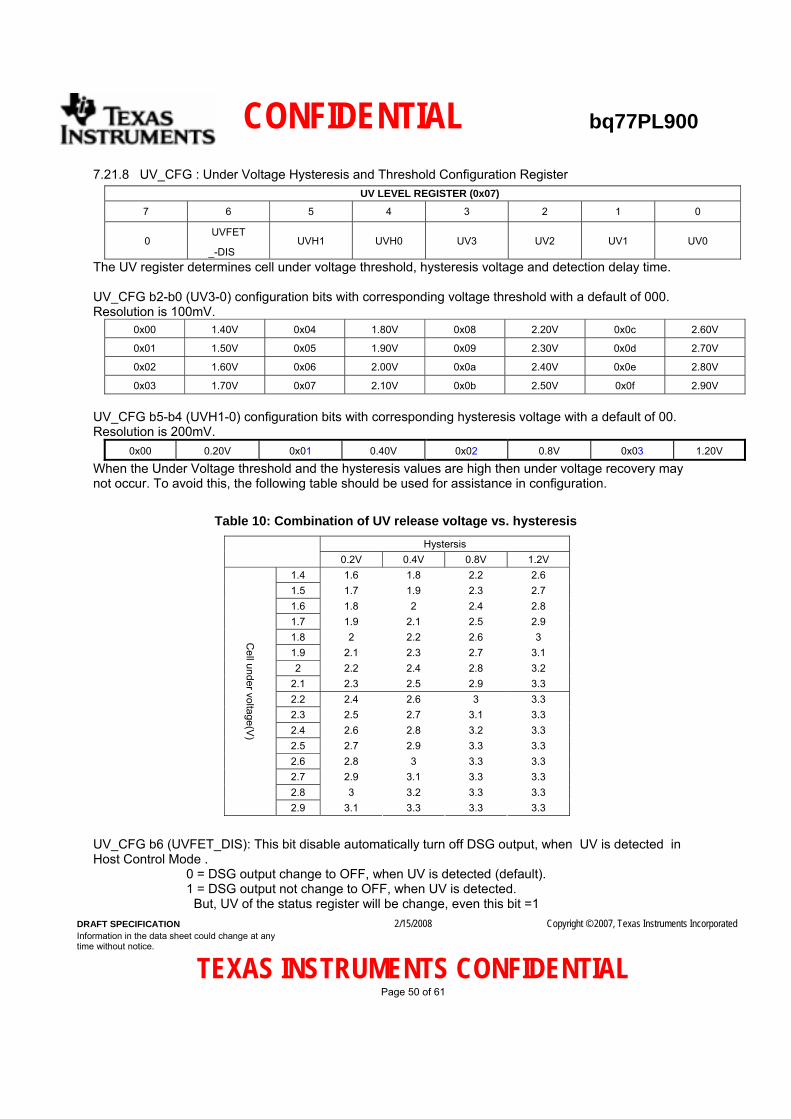
CONFIDENTIAL bq77PL900
DRAFT SPECIFICATION Information in the data sheet could change at any time without notice.
2/15/2008 Copyright © 2007, Texas Instruments Incorporated
TEXAS INSTRUMENTS CONFIDENTIAL Page 50 of 61
7.21.8 UV_CFG : Under Voltage Hysteresis and Threshold Configuration Register UV LEVEL REGISTER (0x07)
7 6 5 4 3 2 1 0
0 UVFET
_-DIS UVH1 UVH0 UV3 UV2 UV1 UV0
The UV register determines cell under voltage threshold, hysteresis voltage and detection delay time. UV_CFG b2-b0 (UV3-0) configuration bits with corresponding voltage threshold with a default of 000. Resolution is 100mV.
0x00 1.40V 0x04 1.80V 0x08 2.20V 0x0c 2.60V
0x01 1.50V 0x05 1.90V 0x09 2.30V 0x0d 2.70V
0x02 1.60V 0x06 2.00V 0x0a 2.40V 0x0e 2.80V
0x03 1.70V 0x07 2.10V 0x0b 2.50V 0x0f 2.90V UV_CFG b5-b4 (UVH1-0) configuration bits with corresponding hysteresis voltage with a default of 00. Resolution is 200mV.
0x00 0.20V 0x01 0.40V 0x02 0.8V 0x03 1.20V
When the Under Voltage threshold and the hysteresis values are high then under voltage recovery may not occur. To avoid this, the following table should be used for assistance in configuration.
Table 10: Combination of UV release voltage vs. hysteresis Hystersis
0.2V 0.4V 0.8V 1.2V
1.4 1.6 1.8 2.2 2.6 1.5 1.7 1.9 2.3 2.7 1.6 1.8 2 2.4 2.8 1.7 1.9 2.1 2.5 2.9 1.8 2 2.2 2.6 3 1.9 2.1 2.3 2.7 3.1 2 2.2 2.4 2.8 3.2
2.1 2.3 2.5 2.9 3.3 2.2 2.4 2.6 3 3.3 2.3 2.5 2.7 3.1 3.3 2.4 2.6 2.8 3.2 3.3 2.5 2.7 2.9 3.3 3.3 2.6 2.8 3 3.3 3.3 2.7 2.9 3.1 3.3 3.3 2.8 3 3.2 3.3 3.3
Cell under voltage(V
)
2.9 3.1 3.3 3.3 3.3
UV_CFG b6 (UVFET_DIS): This bit disable automatically turn off DSG output, when UV is detected in Host Control Mode . 0 = DSG output change to OFF, when UV is detected (default). 1 = DSG output not change to OFF, when UV is detected. But, UV of the status register will be change, even this bit =1
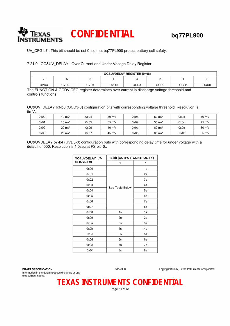
CONFIDENTIAL bq77PL900
DRAFT SPECIFICATION Information in the data sheet could change at any time without notice.
2/15/2008 Copyright © 2007, Texas Instruments Incorporated
TEXAS INSTRUMENTS CONFIDENTIAL Page 51 of 61
UV_CFG b7 : This bit should be set 0 so that bq77PL900 protect battery cell safety.
7.21.9 OC&UV_DELAY : Over Current and Under Voltage Delay Register
OC&UVDELAY REGISTER (0x08)
7 6 5 4 3 2 1 0
UVD3 UVD2 UVD1 UVD0 OCD3 OCD2 OCD1 OCD0
The FUNCTION & OCDV CFG register determines over current in discharge voltage threshold and controls functions. OC&UV_DELAY b3-b0 (OCD3-0) configuration bits with corresponding voltage threshold. Resolution is 5mV.
0x00 10 mV 0x04 30 mV 0x08 50 mV 0x0c 70 mV
0x01 15 mV 0x05 35 mV 0x09 55 mV 0x0c 75 mV
0x02 20 mV 0x06 40 mV 0x0a 60 mV 0x0e 80 mV
0x03 25 mV 0x07 45 mV 0x0b 65 mV 0x0f 85 mV OC&UVDELAY b7-b4 (UVD3-0) configuration buts with corresponding delay time for under voltage with a default of 000. Resolution is 1.0sec at FS bit=0,.
FS bit (OUTPUT_CONTROL b7 ) OC&UVDELAY b7-b4 (UVD3-0) 1 0
0x00 1s
0x01 2s
0x02 3s
0x03 4s
0x04 5s
0x05 6s
0x06 7s
0x07
See Table Below
8s
0x08 1s 1s
0x09 2s 2s
0x0a 3s 3s
0x0b 4s 4s
0x0c 5s 5s
0x0d 6s 6s
0x0e 7s 7s
0x0f 8s 8s

CONFIDENTIAL bq77PL900
DRAFT SPECIFICATION Information in the data sheet could change at any time without notice.
2/15/2008 Copyright © 2007, Texas Instruments Incorporated
TEXAS INSTRUMENTS CONFIDENTIAL Page 52 of 61
Delay time (ms) ,FS =1
UVD<3:0> Internal Count 5Cell 6Cell 7Cell 8Cell 9Cell 10Cell
0x00 0 0 0 0 0 0 0
0x01 2 1.25 1.5 1.75 2 2.25 2.5
0x02 4 2.5 3 3.5 4 4.5 5
0x03 8 5 6 7 8 9 10
0x04 10 6.25 7.5 8.75 10 11.25 12.5
0x05 12 7.5 9 10.5 12 13.5 15
0x06 16 10 12 14 16 18 20
0x07 24 15 18 21 24 27 30
7.21.10 OCD_CFG : Over Current in Discharge Configuration Register
OCD_CFG REGISTER (0x09)
7 6 5 4 3 2 1 0
CBEN ZVC SOR OCDD4 OCDD3 OCDD2 OCDD1 OCDD0
The FUNCTION & OCD_CFG register determines Function and over load detection delay time. OCD_CFG b4-b0 (OCDD4-0) configuration bits with corresponding delay time. Units are in ms and resolution is 20ms or 100ms
0x00 20msec 0x08 180msec 0x10 100msec 0x18 900msec
0x01 40msec 0x09 200msec 0x11 200msec 0x19 1000msec
0x02 60msec 0x0a 220msec 0x12 300msec 0x1a 1100msec
0x03 80msec 0x0b 240msec 0x13 400msec 0x1b 1200msec
0x04 100msec 0x0c 260msec 0x14 500msec 0x1c 1300msec
0x05 120msec 0x0d 280msec 0x15 600msec 0x1d 1400msec
0x06 140msec 0x0e 300msec 0x16 700msec 0x1e 1500msec
0x07 160msec 0x0f 320msec 0x17 800msec 0x1f 1600msec OCD_CFG b5 (SOR): Recover condition from SC and OC with Stand Alone Mode
0 =Recover by attaching a Charger. Recover comparator is active after 12.8sec for OC/SC detection (default)
1 = Recover by SC/OC condition released. Recovery from OC/SC after 12.8sec. OCD_CFG b6 (ZVC): This bit controls the 0V/Pre-charge of GPOD output 0 = Disable GPOD output 0V/Pre-charge mode with Stand Alone (default) 1 = Enable GPOD output 0V/Pre-charge mode with Stand Alone OCD_CFG b7 (CBEN): This bit controls the cell balancing. 0 = Disable cell balancing function (default) 1 = Enable cell balancing function.

CONFIDENTIAL bq77PL900
DRAFT SPECIFICATION Information in the data sheet could change at any time without notice.
2/15/2008 Copyright © 2007, Texas Instruments Incorporated
TEXAS INSTRUMENTS CONFIDENTIAL Page 53 of 61
7.21.11 SCD_CFG : Short Circuit in Discharge Configuration Register
SCD_CFG REGISTER (0x0a)
7 6 5 4 3 2 1 0
SCDD3 SCDD2 SCDD1 SCDD0 SCD3 SCD2 SCD1 SCD0
The SCD_CFG register determines short circuit voltage threshold and detection delay time. SCD_CFG b3-b0 (SCD3-0): These lower nibble bits select the value of the short circuit in discharge voltage threshold with 0000 as the default, units in mV and a resolution of 5mV
0x00 60mV 0x04 80 mV 0x08 100 mV 0x0c 120 mV
0x01 65 mV 0x05 85 mV 0x09 105 mV 0x0d 125 mV
0x02 70 mV 0x06 90 mV 0x0a 110 mV 0x0e 130 mV
0x03 75 mV 0x07 95 mV 0x0b 115 mV 0x0f 135 mV
SCD_CFG b7-b4 (SCDD3-0): These upper nibble bits select the value of the short circuit in discharge delay time. 0000 is the default, units of µs and a resolution of 60µs.
0x00 0µsec 0x04 240µsec 0x08 480µsec 0x0c 720µsec
0x01 60µsec 0x05 300µsec 0x09 540µsec 0x0d 780µsec
0x02 120µsec 0x06 360µsec 0x0a 600µsec 0x0e 840µsec
0x03 180µsec 0x07 420µsec 0x0b 660µsec 0x0f 900µsec
7.21.12 EEPROM : EEPROM Write Enable and COnfiguratin Register
EEPROM REGISTER (0x0b)
7 6 5 4 3 2 1 0
EEPROM7 EEPROM6 EEPROM5 EEPROM4 EEPROM3 EEPROM2 EEPROM1 EEPROM0
EEPROM b7-b0 (EEPROM7-0): These bits enable data write to EEPROM(0x06-0x9a) with 01000001 (0x41). Pre-writing data is available by setting these bits with 01100010 (0x62). Default is 00000000 (0x00).

CONFIDENTIAL bq77PL900
DRAFT SPECIFICATION Information in the data sheet could change at any time without notice.
2/15/2008 Copyright © 2007, Texas Instruments Incorporated
TEXAS INSTRUMENTS CONFIDENTIAL Page 54 of 61
Zero Volt Charging In order to charge cells, the CHG FET must be turned on to create a current path. When the battery voltage (VBAT) is low and the CHG is ON, the pack voltage (VPACK) is as low as the battery voltage. In cases where the level is below the supply voltage for the bq77PL900 is too low to operate, there are two configurations to provide appropriate 0 V/pre-charge function. Common FET mode does not require a dedicated 0V/pre-charge FET. The CHG FET is ON. This method is suitable for a charger that has a 0V/pre-charge function. The second mode is to use a 0V/Pre-charge FET which establishes a dedicated 0V/pre-charge current path by using an additional open drain (GPOD output) for driving an external FET (PCHG FET). This configuration sustains the PACK+ voltage level. Any type of charger can be used with this configuration.
Table 11: 0V Charge Summary
PROTECTION MODE 0V CHARGE TYPE DEMANDED CHARGE
FUNCTION APPLICATION CIRCUIT
Common FET (1) Fast charge Pre-charge
PMS = PACK GPOD ouput not used Host Control
Mode 0V/Pre-Charge FET(2) Fast charge PMS =GND
GPOD output: Drives 0V-charge FET (PCHG FET).
Common FET (1) Fast charge Pre-charge
PMS = PACK GPOD output not used. Stand Alone
Mode 0V/Pre-Charge FET(2) Fast charge PMS = GND
GPOD output: Drives 0V-charge FET (PCHG FET).
7.21.13 Common FET In this mode the PMS pin is connected to PACK+. In this configuration, the charger must have a 0V/pre-charging function which is typically controlled as follows:
• The cell voltage is lower than certain constant voltage (normally about 3.0V/cell) o Apply 0V/Pre charging current.
• The cell voltage is higher than certain constant voltage (normally about 3.0V/cell) o Apply fast charging current.
When the charger is connected and VPMS is greater than or equal to 0.7V the CHG FET is turned ON. The charging current flows through the CHG FET and the back diode of the DSG.
VPACK+ = VBAT + 0.7V (VF: forward voltage of a DSG-FET back diode)+VDS(CHG-FET)

CONFIDENTIAL bq77PL900
DRAFT SPECIFICATION Information in the data sheet could change at any time without notice.
2/15/2008 Copyright © 2007, Texas Instruments Incorporated
TEXAS INSTRUMENTS CONFIDENTIAL Page 55 of 61
bq29500PMS
CHGDSG
BatteryPACK
REG
PACK+CHG-FETDSG-FET
BAT
Charger
I-PC : Pre charge currentI-QC : Quick charge current
CC
CV
I-PC
I-QC
GPOD
Open
bq29500PMS
CHGDSG
BatteryPACK
REG
PACK+CHG-FETDSG-FET
BAT
Charger
I-PC : Pre charge currentI-QC : Quick charge current
CC
CV
I-PC
I-QC
GPOD
Open
Figure 23: Common FET Circuit Diagram
When the PACK pin voltage is maintained at higher than 0.7V and the pre-charging current is maintained, the PACK voltage and BAT voltage are under the minimum bq77PL900 supply voltage so the bq77PL900 regulator is inactive. When the BAT voltage rises and the PACK pin voltage reaches bq77PL900 minimum supply voltage, an internal 3.3V regulator is turned ON. Then, the CHG FET state is controlled by UVP and OVP functions. When the all the cell voltages reach fast charge voltage (about 3.0V per cell), the charger starts fast charging mode.
PACK
PMS
CHG
REG23.3V
Charge current 0V & Pre-chg current
Quick charge current
Battery voltage
DSG
0A
0V
0V
0V
CHG=L by 0V charge control
OV charge & Pre-charge mode Quick charge mode
0V
“L”
0V
“L”
Operating voltage
0V charge disable voltage
DSG=L by 0V charge control
Figure 24: Signal Timing of Pins during 0 V/Pre-charging

CONFIDENTIAL bq77PL900
DRAFT SPECIFICATION Information in the data sheet could change at any time without notice.
2/15/2008 Copyright © 2007, Texas Instruments Incorporated
TEXAS INSTRUMENTS CONFIDENTIAL Page 56 of 61
7.21.14 0V/Pre-Charge FER in Host Control Mode In this configuration, the charger doesn’t need to support a pre-charge function. Thus, the Host controller and bq77PL900 must limit the fast charging current to a suitable 0V/Pre-charge level. The PMS pin is connected to GND and a 0V/pre-charge current flow through a dedicated 0V/pre-charge FET (PCHG FET).
bq29500
PMS
CHGDSG
Battery
PACK
REG
GPOD
PCHG-FET
CHG-FETDSG-FETBAT PACK+
Charger
I-QC : Quick charge current
CC
CV
I-QC
R(PCHG)
bq29500
PMS
CHGDSG
Battery
PACK
REG
GPOD
PCHG-FET
CHG-FETDSG-FETBAT PACK+
Charger
I-QC : Quick charge current
CC
CV
I-QC
R(PCHG)
Figure 25 : 0V/Pre-charge FET circuit in Host Control Mode
The 0V/pre-charge FET is driven by the GPOD output. By set 1 at GPOD bit , then GPOD output turns ON, then the PCHG FET. The 0V/pre-charge current is limited by the 0V/pre-charge FET (PCHG FET) and a series resister (R(PCHG)) as below.
I0V/PCHG = ID = ( VPACK+ – VBAT – VDS ) / RP A load curve of the PCHG FET is shown below. When the gate – source voltage (VDS) is high enough, the FET operates in the linear region and has low resistance. By approximating VDS as 0V, the 0V/pre-charge current (I0V/PCHG) is expressed as below.
I0V/PCHG = (VPACK+ – VBAT) / RP
VDS
ID ID = (VPACK-VBAT-VDS)/PR
Figure 26 : 0V/PCHG FET ID and VDS characteristics

CONFIDENTIAL bq77PL900
DRAFT SPECIFICATION Information in the data sheet could change at any time without notice.
2/15/2008 Copyright © 2007, Texas Instruments Incorporated
TEXAS INSTRUMENTS CONFIDENTIAL Page 57 of 61
During the 0V/pre-charge, the CHG FET is turned OFF and the PCHG FET is turned ON. When the Host controller detects that all the cell voltage have reached the fast charge threshold, it then turns ON the CHG FET and turns OFF the PCHG FET. The signal timing is shown below. The CHG, DSG and PCHG FETs are turned OFF when the charger is connected. Then, the charger applies its maximum output voltage (constant voltage mode output voltage) to the PACK+ pin. Then, the bq77PL900 3.3V regulator becomes active and supplies power to the Host controller. As the Host controller starts up, it turns on the GPOD output and the 0V/pre-charge current begins to flow. In this configuration, attention is needed to control high power consumption at the PCHG FET and the series resistor (RP). The highest power is consumed at 0V cell voltage (highest voltage between PACK+ and BAT pins) and it results in highest heat generation. For example, the power consumption in 10 series batteries with 42V fast charge voltage and 1K Ohms RP is expressed as below.
IOV/PCHG = (42V – 0.0V) /1kΩ = 42mA (Power Consumption at RP) = 42V x 42mA = 1.6W
It is recommended to combine the resister (RP) and the thermistor to reduce the consumption. Once the cell voltage reaches the fast charge threshold, the host controller turns ON the CHG and DSG FETs and also turns OFF the PCHG FET.
PACK
CHG
REG23.3V
Charge current 0V & Pre-chg current
Quick charge current
Battery voltage
DSG
0A
0V
“L”
CHG-FET = ON
DSG-FET = ON by uC
OV & Prechargecharge mode
Quick chargemode
0V
0V
uP : Active
GPOD
0V
Charge CV
CHG-FET = OFF
PCHG FET =ON OFFOFF
“L”
Figure 27 : Signal Timing of Pins during 0 V charging and pre-charging (Pre-charge FET) with Host Control Mode

CONFIDENTIAL bq77PL900
DRAFT SPECIFICATION Information in the data sheet could change at any time without notice.
2/15/2008 Copyright © 2007, Texas Instruments Incorporated
TEXAS INSTRUMENTS CONFIDENTIAL Page 58 of 61
7.21.15 0V/Pre-Charge FER in Stand Alone Mode The circuit configuration is the same as 0/Pre-charge FET In Host Control Mode although in Stand Alone Mode the bq77PL900 automatically turns on GPOD output. When the battery voltage reaches “0V the charger disable voltage” (=PMS disable voltage), GPOD output is turned OFF, and then the DSG and CHG FETs are controlled by internal UV comparator function. To activate this mode, set OCDELAY register [ZVC].
bq29500
PMS
CHGDSG
Battery
PACK
REG
GPOD
PCHG-FET
CHG-FETDSG-FETBAT PACK+
Charger
I-QC : Quick charge current
CC
CV
I-QC
R(PCHG)
bq29500
PMS
CHGDSG
Battery
PACK
REG
GPOD
PCHG-FET
CHG-FETDSG-FETBAT PACK+
Charger
I-QC : Quick charge current
CC
CV
I-QC
R(PCHG)
Figure 28 : 0V/Pre-charge FET Circuit Diagram In Stand Alone Mode
PACK
CHG
REG23.3V
Charge current 0V & Pre-chg current
Quick charge current
Battery voltage
DSG
0A
0V
“L”
CHG-FET = ON
DSG-FET = ON by uC
OV & Prechargecharge mode
Quick chargemode
0V
0V
GPOD
0V
Charge CV
CHG-FET = OFF
PCHG FET =ON OFF
“L”
0V charge disable voltage
Figure 29: Signal Timing of Pins during 0V/Pre-charging (PCHG FET) In Stand Alone Mode
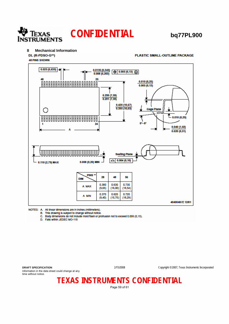
CONFIDENTIAL bq77PL900
DRAFT SPECIFICATION Information in the data sheet could change at any time without notice.
2/15/2008 Copyright © 2007, Texas Instruments Incorporated
TEXAS INSTRUMENTS CONFIDENTIAL Page 59 of 61
8 Mechanical Information
CONFIDENTIAL bq77PL900
DRAFT SPECIFICATION Information in the data sheet could change at any time without notice.
2/15/2008 Copyright © 2007, Texas Instruments Incorporated
TEXAS INSTRUMENTS CONFIDENTIAL Page 60 of 61
9 Reference Schematic

CONFIDENTIAL bq77PL900
DRAFT SPECIFICATION Information in the data sheet could change at any time without notice.
2/15/2008 Copyright © 2007, Texas Instruments Incorporated
TEXAS INSTRUMENTS CONFIDENTIAL Page 61 of 61
IMPORTANT NOTICE
Texas Instruments (“TI”) warrants performance of its semiconductor products to the mutually agreed upon written
specifications applicable at the time of sale, in accordance with TI’s standard warranty. TI assumes no liability for applications
assistance, customer product design, software performance or infringement of patents, unless expressly agreed to in a written
contract with the customer.
In order to minimize risks associated with the customer’s applications, adequate design and operating safeguards should be
provided by the customer to minimize inherent or procedural hazards. Testing and other quality control techniques are utilized
to the extent TI deems necessary to support its product warranty. Specific testing of all parameters of semiconductor products
is not necessarily performed. Only those tests mutually agreed upon in writing, including failure modes & effects analyses, will
be performed for custom product, except as mandated by government requirements.
TI SEMICONDUCTOR PRODUCTS ARE NOT DESIGNED, INTENDED, AUTHORIZED, OR WARRANTED TO BE
SUITABLE, FOR USE IN LIFE-SUPPORT APPLICATIONS, DEVICES OR SYSTEMS OR OTHER CRITICAL
APPLICATIONS (i.e., applications which may involve potential risks of death, personal injury, or severe property or
environmental damage). Inclusion of TI products in such applications is understood to be fully at the risk of the customer and
requires written approval from an appropriate TI officer. Questions concerning potential risk applications should be directed to
the appropriate TI sales contact.
TI does not warrant or represent that any license, either expressed or implied, is granted under any patent right,
copyright, maskwork right, or other intellectual property right of TI covering or relating to any combination, machine, or process
in which TI semiconductor products or services might be or are used.