Embed Size (px)
Citation preview

Introduction
The electronics industry is undergoing a major shift—one in which software is eclipsing hardware as the main driver of system development cost, schedule, and risk. In a wide variety of products, software applications or “apps” have become the main differentiator. As such, systems companies are increasingly expecting their semiconductor suppliers to provide not just silicon, but complete hardware/software systems ready for applications deployment.
In the EDA360 vision paper published by Cadence in 2010, the creation of application-ready hardware/software systems is called “System Realization.” One requirement for System Realization is concurrent hardware/software development and verification throughout the design flow—all the way from an initial specification to a final product. System Realization requires a continuum of development platforms that is open in terms of support for standards and third-party tools, connected to allow fast migration between platforms and links to implementation, and scalable to provide sufficient performance and capacity, as well as high-volume software distribution
Customer experience shows that the traditional approach of designing hardware first, and appending software later, no longer works. At advanced process nodes, software development now consumes 50% or more of the cost—and that percentage is rising. Embedded software complexity now includes millions of lines of code in many consumer products. System integration and bring-up is the major time-to-market challenge for many OEMs, and can take 50% of the overall development time, according to discussions with design teams.
The chart below shows the explosive hardware and software development costs for systems-on-chip (SoCs) at advanced process nodes—costs that are projected to reach $100 million at 32nm and below. If such costs cannot be contained, only a handful of high-volume SoCs will be designed at future process nodes, leaving most applications to run on generic hardware that is not optimized for the applications.
Concurrent Hardware/Software Development Platforms Speed System Integration and Bring-UpAuthor: Ran Avinun, Cadence Design Systems, Inc.
Hardware/software development platforms such as virtual prototyping, acceleration/emulation, and FPGA prototyping are typically provided as fragmented and isolated point tools. This paper shows how a continuum of open, connected, and scalable platforms can greatly reduce system integration and bring-up times for application-ready, hardware/software systems.
Contents
Introduction .................................1
EDA360 and System Realization ...2
Hardware/Software Development
Platforms and Their Uses ..............3
Today’s Disconnected Solutions and
Their Challenges ..........................5
System Development Suite ...........7
Virtual System Platform ................9
Incisive Verification Platform ...... 10
Verification Computing Platform 11
Rapid Prototyping Platform ........ 12
Conclusion ................................. 13

160
140
120
100
80
60
40
20
0
$ M
illio
ns
90nm 65nm 45nm 32nm 22nm
Software
Architecture, Design, and Verification
Implementation and Manufacturing
Figure 1: Software and architectural design costs are rising rapidly for advanced SoCs (Source: IBS, 2009)
Developers today are using a mix of platforms for hardware/software integration and debugging. These may include virtual prototypes (or virtual platforms), simulation, acceleration/emulation, and FPGA-based prototypes. Typically these development platforms are disconnected point tools. They represent proprietary, fragmented, and incomplete solutions that don’t allow easy migration between tools, or provide enough scalability to meet performance/capacity and volume demands.
This paper describes existing hardware/software development platforms and their advantages and limitations. It also presents the System Development Suite from Cadence, a key enabling technology for System Realization. The suite provides a concept-to-prototype continuum of open, connected, and scalable platforms that supports the concurrent development of application-ready hardware/software systems.
EDA360 and System Realization
EDA360 is an expanded vision of EDA that encompasses embedded software as well as hardware, and provides support for both IP integration and creation. System Realization is the development of a complete hardware/software system ready for applications deployment, including silicon, “bare metal” (hardware-dependent) software, middleware, and operating system. A system also includes IC packages, one or more printed circuit boards, and an enclosure.
System Realization includes SoC Realization, which is the creation of an individual system-on-chip including low-level software, and Silicon Realization, which is the design and verification of analog and digital blocks, subsystems, and ICs.
System Realization
SoC Realization
Silicon Realization
EDA360App App App App
Silicon
Fabric
DriverCPU
Sub-system
DriverMemory
Sub-system
DriverI/O
Sub-system
DriverCustomer
Sub-system
HW/SW Platforms
OS + Middleware
Kernel
Figure 2: System Realization represents the creation of complete hardware/software platforms up to the applications level of the software stack
www.cadence.com 2
Concurrent Hardware/Software Development Platforms Speed System Integration and Bring-Up
The importance of software applications is leading to a new development methodology in which companies begin projects with an understanding of the needs of the applications that will run on the system. They then use that understanding to develop an optimized platform that will support the applications. This “application-driven” design approach is different than traditional design flows, in which the silicon is built first and the software is tacked on later by different teams or companies.
Nothing new is easy, however, and System Realization presents several interesting questions:
• How can I architect a system? At the highest level of abstraction, developers specify the functionality they need and then define a hardware/software architecture. This process involves high-level modeling and performance analysis. Few automated tools exist today, and most high-level models are rewritten by downstream hardware and software designers.
• How do I do hardware/software co-development? In traditional flows, hardware and software are developed separately by teams who have little visibility into what the other is doing. Software is typically developed after silicon is created. That’s no longer viable in today’s fast-paced, competitive environment – software development must start long before silicon.
• How do I validate hardware/software systems? Hardware and software verification and debug have been completely separate. Hardware designers have access to technologies like metric-driven verification, but software verification is ad-hoc. Without concurrent hardware/software verification, and advanced verification techniques available to both teams, bugs in the hardware/software interface are easily missed.
Several types of system development platforms are beginning to address these challenges, but existing solutions have many limitations, as noted in the sections that follow.
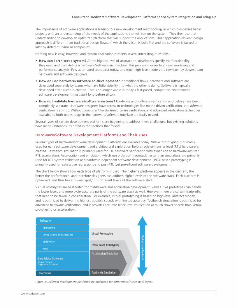
Hardware/Software Development Platforms and Their Uses
Several types of hardware/software development platforms are available today. Virtual prototyping is primarily used for early software development and architectural exploration before register-transfer level (RTL) hardware is created. Testbench simulation is primarily used for RTL hardware verification with expansion to hardware-assisted RTL acceleration. Acceleration and emulation, which run orders of magnitude faster than simulation, are primarily used for RTL system validation and hardware-dependent software development. FPGA-based prototyping is primarily used for exhaustive regressions and post-RTL (yet pre-silicon) software development.
The chart below shows how each type of platform is used. The higher a platform appears in the diagram, the better the performance, and therefore designers can address higher levels of the software stack. Each platform is optimized, and thus has a “sweet spot,” for different layers of the software stack.
Virtual prototypes are best suited for middleware and application development, while FPGA prototypes can handle the lower levels and more cycle-accurate parts of the software stack as well. However, there are certain trade-offs that need to be taken in consideration. For example, virtual prototyping is based on high-level abstract models, and is optimized to deliver the highest possible speeds with limited accuracy. Testbench simulation is optimized for advanced hardware verification, and it provides accurate block-level verification at much slower speeds than virtual prototyping or acceleration.
FPGA-based Prototyping
Virtual Prototyping
Acceleration/Emulation
Software
Hardware Testbench Simulation
Applications
Device Control and Scheduling
Middleware
RTOS
Bare Metal SoftwareDrivers, Firmware, Diagnostics, Boot Load
Performance Trade-off
Figure 3: Different development platforms are optimized for different software stack layers
www.cadence.com 3
Concurrent Hardware/Software Development Platforms Speed System Integration and Bring-Up

Virtual Prototyping
Virtual prototyping is a software model of a system that can be used for early software development and SoC/system architectural analysis. Virtual prototyping includes processor and peripheral models that may run at or near real-time speeds, potentially supporting pre-silicon development of the entire software stack up to the applications level. Virtual prototyping solutions (sometimes called “virtual platforms”) may come with tools to help develop models, and they also usually provide a simulation and debugging environment. While early virtual prototyping solutions required proprietary models, many now use SystemC models based on the Open SystemC Initiative® (OSCI) transaction-level modeling (TLM) standard and the IEEE-1666 SystemC® standard.
In addition to early software development, virtual prototyping can be used for software distribution, system development kits and customer demos. In post-RTL software development, for example, virtual prototyping can be used as a low-cost replacement for silicon reference boards distributed by semiconductor companies to software developers in systems (OEM) companies. Compared to reference boards, virtual prototyping provides much better debug capabilities and iteration time, and therefore can accelerate the post-silicon system integration process.
The bottom line is that virtual prototyping reduces software development costs and time to market. It improves quality and enables earlier and more frequent hardware/software integration. It can also provide fairly complete software that helps hardware designers verify designs before detailed implementation.
The primary tradeoff is that virtual prototypes lack timing-aware hardware accuracy. They also require their own high-level abstraction models. Other common limitations include difficulty in plugging in third-party tools, separate hardware and software debug environments that require a long manual data transfer process between hardware and software teams, and performance that doesn’t scale. Support for programming and debugging multi-core SoCs is lacking in some commercial offerings.
Testbench Simulation
Testbench simulation has been the workhorse of hardware RTL verification for many years, and it remains so today. Advanced simulators support metric-driven verification, a methodology in which an executable verification plan tracks coverage and monitors and checks metrics to guide the verification flow. These metrics are typically used in conjunction with constraint-driven randomized test generation. A 2011 Accellera standard, the Universal Verification Methodology (UVM), supports metric-driven verification and will build a foundation for interoperable verification IP (VIP). Testbench simulation is now expanding to serve as a component of simulation acceleration and SystemC TLM for chip and system-level verification.
The primary disadvantage of RTL simulation is that simulation slows down in a non-linear fashion as the design size increases. For this reason, simulation is generally aimed at hardware verification. RTL simulation often needs to be complemented with acceleration and/or emulation to make verification scalable to large blocks and systems.
Acceleration and Emulation
Acceleration and emulation provide hardware-assisted verification that runs orders of magnitude faster than simulation while providing RTL cycle accuracy. They combine high capacity with excellent debug capabilities and enable fast bring-up and iteration time, although they provide limited speed and a larger footprint compared to FPGA-based prototyping and the real silicon. Brief definitions of RTL acceleration and emulation are as follows:
• In acceleration, portions of the design are typically running on the hardware while a simulation testbench runs on the workstation. If the testbench is transaction-based, the result is transaction-based acceleration.
• In emulation, the entire design and verification environment is generally running on the hardware. In addition to the hardware in the emulation box, portions of the design or the testbench may also be running on external target hardware through in-circuit emulation.
Acceleration speeds up an existing simulator, and should provide most or all of the benefits of simulation, including constrained-random test generation, coverage metrics, and full debug visibility. With emulation, the verification environment is self-contained within the hardware, and users can plug in real hardware and interfaces, run drivers, boot an operating system, or test software applications. Emulation offers extremely fast bring-up times and run times of several MHz, but typically does not have all the benefits of simulation, such as stimulus randomization.
www.cadence.com 4
Concurrent Hardware/Software Development Platforms Speed System Integration and Bring-Up

Therefore, acceleration is commonly run in the hardware/software integration flow, where a simulation-like development and debug environment is important. Emulation is used when everything including the testbench can be moved into hardware, and execution speed is paramount. This allows system-level scenario validation, real-world testing, and software development.
Acceleration has traditionally used a signal-level interface that results in a communications channel overhead between the workstation and the accelerator. Transaction-based acceleration is an advanced technique in which the interface is abstracted to a transaction (message) level. As shown below, the transaction-based communication between the workstation and the hardware is handled with the Accellera Standard Co-Emulation Modeling Interface (SCE-MI 2.1) standard, along with a “proxy” model on the workstation side and a bus-functional model (BFM) on the hardware side.
Testbench
PROXY
SCEMI
SCEMI
BFM
Workstation Hardware
DesignUnderTest
Comm
unicationChannel
Figure 4: Transaction-based acceleration reduces communication channel overhead
Many design and verification teams are now using transaction-based acceleration as a “bridge” between simulation and in-circuit emulation.
FPGA-Based Prototyping
Nearly all ASIC and SoC development projects use FPGA-based prototyping. In many cases these prototypes are custom-built boards. Developing such boards involves a considerable design effort and may result in bring-up times of months. Today one can purchase off-the-shelf FPGA-based prototyping boards and the corresponding FPGA partitioning and implementation software, but long bring-up times are still the biggest problem with this technology.
The reward with FPGA-based prototyping is extremely fast execution speeds, in the 10s of MHz range—not real time but fast enough for post-RTL software development and exhaustive regression testing. FPGA-based prototyping may run an order of magnitude faster than an emulator, and can connect to real-world hardware and interfaces. The small footprint and the affordable price of FPGA-based prototypes make it possible to deploy them in volume to many software developers, thus further speeding up the development cycle.
However, FPGA-based prototypes offer limited debugging capabilities. It is typically up to the user to define a limited number of signals to be observed. Depending on what FPGA debug tools are used, the probed signals will be represented at the netlist level, making it cumbersome for the user to match them to the RTL signals in their design. Using an external logic analyzer for at-speed debug is also a widely used approach, but it also requires designers to bring the internal signals that are to be observed to an external FPGA pin, and that has to be done up front as well.
Today’s Disconnected Solutions and Their Challenges
Because no one development platform can serve all needs, a continuum of integrated solutions is needed. The components of this continuum—virtual prototyping, acceleration/emulation, testbench simulation, and FPGA-based prototyping—are all available today, although at this writing only Cadence provides all of these platforms. Until now, assembling a continuum of development platforms has typically involved purchasing disconnected point tools or building “do it yourself” virtual prototyping models or FPGA boards, with little focus on the integration between them. Models typically cannot be shared between platforms and must be reworked at each step.
www.cadence.com 5
Concurrent Hardware/Software Development Platforms Speed System Integration and Bring-Up

The biggest limitation with existing hardware/software development platforms, therefore, is the overall flow. Today’s flows are often based on proprietary formats and are closed to third-party tools. Today’s flows require manual migration from one platform to another—which may take months—and are thus fragmented and counter-productive. They are non-scalable to the demands of complex hardware/software design projects, and are thus limited. “Closed, fragmented, and limited” is the opposite of the “open, connected, and scalable” approach that is needed.
The result: long times to market, lower quality, and development costs approaching $100M at advanced process nodes. Three examples of today’s “disconnect” are provided below.
Disconnect: Architectural Software Development and Block-Level Design/Verification
Virtual prototypes allow architectural software development, but they are “islands” disconnected from the downstream design and verification flow. The models that they are comprised of are typically not synthesizable (OSCI TLM2 has no synthesizable subset as of this writing) and cannot be used for implementation via high-level synthesis. In addition to lacking a path to implementation, virtual prototyping typically has no connection with the block-level RTL verification and debug environment, whether it’s provided by testbench simulation or acceleration.
Models provided by virtual prototype vendors are often proprietary to the solution and are not configurable by the user, and thus cannot be reused or migrated to other platforms. Models must thus be redesigned from one level to the next, adding to the risk that the implementation won’t match the initial spec. It may be difficult to create or change models not provided by the vendor, and impossible to bring TLM or RTL models for pre-existing IP or verification IP into the virtual prototype simulation.
Customers who have tried to use virtual prototypes in isolation have often found that the virtual models do not reflect the reality of what gets built into the hardware, resulting in long integration and debug times. Congruency between virtual models and the actual implementation requires the combination of virtual prototypes with cycle-accurate RTL.
Another disconnect occurs because the high-level models used for virtual prototyping don’t provide the timing and power information that is needed for detailed architectural analysis, optimization, and multi-core software/system design. Historically, attempts to produce cycle-accurate virtual prototyping required detailed design knowledge. This resulted in lengthy schedules to produce these models, and RTL was often completed before cycle- accurate virtual prototypes were accurate enough. In addition, the runtime performance was degraded with this timing accuracy, limiting the amount of software that can be conceivably executed and analyzed.
Disconnect: Simulation, Acceleration, and Emulation
Acceleration and emulation are often separate solutions, making it necessary to buy and maintain two hardware “boxes” at substantial expense. In such cases there is no easy migration path between simulation, acceleration, and emulation, and no capability that will allow switching between these modes on the fly, which is especially important during initialization and bring-up. Also, there is usually no connection to the FPGA-based prototyping environment, which is unfortunate because an emulator can potentially work with an FPGA prototype to offer greater debug visibility and turnaround times.
Emulation may be isolated from the simulation environment, lacking features such as metric-driven verification and the ability to run verification IP. The debug environment may be different from simulation and more limited. In some cases, long compilation times offset some of the run time benefits acceleration and emulation provide, and should be considered along with any run time comparisons.
Finally, power verification and analysis are becoming more and more critical, especially at abstraction levels that allow designers to test their power structures as well as measure the power more accurately. Acceleration is a natural expansion of testbench simulation, and therefore designers would like to run their system validation with the low power verification techniques used in simulation. Emulation, on the other hand, provides an excellent opportunity to analyze the overall power consumption, including the hardware and the software in the context of full SoC or full system. These techniques have not been available in the past but are starting to evolve in the market.
www.cadence.com 6
Concurrent Hardware/Software Development Platforms Speed System Integration and Bring-Up

Disconnect: FPGA-Based Prototyping from the ASIC Design Flow
As mentioned, the biggest problem with FPGA-based prototypes is bring-up time, which can take several months. One reason is that FPGA prototyping is a formidable project in itself using different tools and methodologies compared to an ASIC/SoC flow, and it requires heavy investment of human resources. Customer experience suggests that custom FPGA boards may take three months to design and incur NRE costs up to $150,000, excluding the cost of resources and the potential time-to-market risk.
Even if a design team purchases pre-built boards and software, implementing ASIC/SoC functionality in FPGAs can take many months. The initial bring-up in particular is a long and time consuming process that often requires modifications to the ASIC RTL code to make it suitable for FPGAs. Bring-up typically involves memory remodeling, clock tree modifications, partitioning the design into multiple FPGAs, inserting pin-multiplexing logic, adding rate-adaption logic to connect to external interfaces, and adding some probing and debug capabilities. As a result, the design undergoes major transformations, and validating that these transformations have not changed the functionality of the design is a major challenge in itself that can add weeks or months to the prototyping bring-up.
Although automatic partitioning tools are available, they are not easy to use and require not only a deep knowledge of the design itself but also of the FPGAs that are used. The other alternative, doing manual partitioning and preparing the design based on an understanding of the architecture of the FPGA-based boards, is obviously not easy either. In any case, bringing up an FPGA-based prototype today requires special FPGA experts that are typically not a natural part of the ASIC development team.
System Development Suite
The Cadence® System Development Suite is a set of concurrent hardware/software development and verification platforms that spans the design cycle from early software development to post-RTL debugging and system integration. It supports all levels of the software stack and multiple levels of design abstraction. The goal of the suite is to lower costs and speed time-to-market by greatly accelerating system integration, system validation and bring-up times.
Unlike current solutions, the System Development Suite provides an open, connected, and scalable set of development platforms. It’s based on standards, it allows easy migration between platforms, and it can scale to meet the performance, capacity, and software distribution volume needs of present and future electronic systems. The suite provides a key enabling technology for System Realization and thus represents significant progress in realizing the EDA360 vision.
Key components of the System Development Suite are as follows:
• The Virtual System Platform, announced May 2011 in “early adopter” mode, is a standards-based (SystemC TLM) virtual prototyping solution for early software development at the architectural level. It provides system analysis and optimization and offers an alternative to silicon prototyping reference boards that are distributed to software developers. It provides an integrated hardware/software debug environment with unique multi-core capabilities, is connected to the RTL verification flow, and automates and accelerates the creation of virtual prototypes.
• The Palladium® XP Verification Computing Platform, announced April 2010 at the same time as the EDA360 vision paper, provides RTL acceleration, emulation and simulation. A “hot swap” capability allows instant migration between these technologies.
• The Rapid Prototyping Platform, available May 2011, consists of FPGA-based prototyping boards supporting up to 30M ASIC gates capacity and complementary software enabling fast design implementation, automatic multi-FPGA partitioning and a powerful debug capability.
• The Incisive® Verification Platform, available since 2003, is a family of verification tools optimized for block-level verification with testbench simulation as the focal point. It supports a number of standard languages including Specman®/e, SystemVerilog, and SystemC, as well as the UVM.
All of these platforms work together, and all leverage components of the widely distributed Incisive Verification Platform. For example, the Virtual System Platform, Verification Computing Platform, and Rapid Prototyping Platform use the Incisive SimVision debug user interface. The Virtual System Platform and the Incisive Verification Platform share a unified simulator, and the Verification Computing Platform shares the same compile and run time environment with the Incisive Verification Platform.
www.cadence.com 7
Concurrent Hardware/Software Development Platforms Speed System Integration and Bring-Up

The diagram below shows what portions of the development cycle each platform is optimized for. While the “sweet spot” of the Virtual System Platform is pre-RTL, architectural-level software development, it can also be used in a post-RTL mode to generate virtual prototypes that provide an alternative to reference boards.
Hardware
Software
Virtual SystemPlatform
Rapid PrototypingPlatform
Verification ComputingPlatform
Incisive VerificationPlatform
Architecture-LevelSW Development
Block/Chip-LevelVerification
System Validation
Prototype SWDevelopment
Conc
ept
Prod
uct
Figure 5: The Cadence System Development Suite offers a concurrent, integrated hardware/software development and debugging flow that works throughout the development cycle.
While each of the platforms by itself provides best-in-class capabilities, what’s most notable is how they work together in an open, connected, and scalable flow, as shown by the following examples.
Open—Standards and Third-Party Ecosystem
The Cadence System Development Suite is based on industry standards. For example, the Virtual System Platform uses the OSCI, TLM, and IEEE-1666 SystemC standards, and provides an automated TLM2 code generator that can take input in the Accellera IP-XACT format standard. The Incisive Verification Platform supports standard languages such as e, SystemC, and SystemVerilog, in addition to UVM 1.0. The Verification Computing Platform also supports UVM as well as the Accellera Standard Co-Emulation Modeling Interface (SCE-MI) in addition to the same language standards supported by the Incisive Verification Platform. The Rapid Prototyping Platform uses an ASIC RTL-based flow with standard design languages and supports standard interfaces such as PCIe, Ethernet, and USB.
The suite offers considerable third-party support. The Virtual System Platform supports third-party processor models including ARM® Fast Models and Imperas Open Virtual Platform (OVP) models. It also supports third-party software debuggers such as ARM, Lauterbach, and GDB. Altera Stratix IV hardware and software is embedded in the Rapid Prototyping Platform.
Connected—Easy Migration Between Platforms
With disconnected point tools, it may take months to migrate between development platforms. The System Development Suite offers a connected flow from early software development to final prototyping, allowing easy migration between platforms. The suite is connected to implementation through common models and a natural flow through TLM design and verification.
For example, the Virtual System Platform and the Incisive Verification Platform use common hardware/software debugging, and share a mixed TLM/RTL environment with a unified simulator and common verification IP. The Incisive Verification Platform and the Verification Computing Platform share compile, debug, and run time environments and support common accelerated verification IP. This connectivity enables flexibility for performance and architectural analysis and optimization at early stages of the project, and easily incorporates RTL for fully accurate timing and power analysis.
The Verification Computing Platform’s SpeedBridge® adapters, which allow connections to real-world hardware for in-circuit emulation, can also be used with the Rapid Prototyping Platform. The Rapid Prototyping Platform and the Verification Computing Platform share the same compile environment and memory models. In addition, the Rapid Prototyping Platform uses the Verification Computing Platform to verify the functionality of the FPGA-based prototype configuration.
www.cadence.com 8
Concurrent Hardware/Software Development Platforms Speed System Integration and Bring-Up

By reusing and building upon bring-up preparations that have been done in each previous development phase, instead of re-doing them over and over again, this continuum of development platforms and its integrated flow improve productivity and the user experience. Most importantly, the flow enables the fast migration from one design phase to another while hardware and software continue to be developed concurrently. This connected flow accelerates the pre-silicon system development and verification process and the post-silicon system integration time to ensure achievement of a higher level of quality, earlier.
Scalable—Meeting Performance and Capacity Demands
By allowing easy migration between platforms, the System Development Suite lets developers scale “up” or “down” by moving to higher or lower levels of abstraction. Developers can trade off performance against features and functionality. The ability to “hot swap” between acceleration/emulation and the Incisive simulation environment without recompilation is one example.
The Virtual System Platform offers features that make it possible to scale from single-core to multi-core software development and debug with performance reaching up to hundreds of MHz (or silicon speed in some cases). Virtual prototypes can be easily distributed to large numbers of software developers. The Rapid Prototyping Platform scales up to 30M ASIC gates and tens of MHz execution speed. It can also produce affordable “replicates” in high volumes for software development. And the Verification Computing Platform offers configurations up to 2 billion gates and supports up to 512 simultaneous users with a granularity of 4M gates.
Virtual System Platform
The Cadence Virtual System Platform is a software development platform built on top of an abstracted model of hardware. It enables the early development of hardware-aware, OS, and application software, and greatly reduces the risk of discrepancies between the abstracted hardware model and the eventual RTL. It provides automation for easy creation of SystemC abstracted hardware models, provides system analysis, and allows a close connection between hardware and the software teams. Unlike previous generation solutions the Virtual System Platform supports fully integrated multi-core hardware/software debugging and provides an integrated connection to the RTL flow.
The ability to incorporate integrated RTL execution in the virtual platform provides a unified debugging experience, and enables software analysis and architectural tradeoffs with the abstracted hardware model or the cycle-accurate RTL. As a result of these capabilities, design teams can develop and debug software at all levels in the software stack, from device drivers to applications.
Integrated Multi-Core Hardware/Software Debug
The Virtual System Platform debug environment is built on top of Cadence SystemC debug environment and has been extended to support software and system concepts. The platform thus provides multi-core debugging, enabling processor-specific breakpoints and software execution control. It provides complete hardware/software visibility and controllability including fully synchronized breakpoints, single stepping, and memory/register/variable tracing. The GUI provides fully synchronized, coherent multi-core hardware/software debugging and can reflect a software view, a hardware view, or a combination of the two. Developers can set up specific breakpoints across the independent multi-core domains and observe and control parallel execution.
The exported virtual prototype can be connected to third party debug and analysis solutions. These include the ARM RealView® debugger for ARM Fast Models, as well as Imperas verification, analysis, and prototyping tools for Imperas CPU models.
Connection to RTL Flow
If incorporation of RTL models or use of a functional verification testbench is required, designers can easily add the Incisive Verification Platform to the mix. The SystemC TLM models can be mixed with RTL models in any language supported by Incisive. This connection also enables the use of testbench languages such as Specman/e and SystemVerilog, and supports UVM.
Finally, RTL can be accelerated using the Verification Computing Platform in a mixed SystemC/RTL environment. Since the Virtual System Platform, Incisive Verification Platform, and the Verification Computing Platform were architected and built from the same unified simulator base, the environment provides high performance, consistent user experience, and fast migration.
www.cadence.com 9
Concurrent Hardware/Software Development Platforms Speed System Integration and Bring-Up

Open SystemC Device Platform Creation
The Virtual System Platform uses models that would be naturally created in the course of a design, rather than forcing the use of proprietary models usable for virtual prototyping only. The Virtual System Platform features tight interoperability with ARM Fast Models, which cover the most recent ARM processors and typically run at or close to silicon speed, reaching 100s of MHz. The platform also supports Imperas open-source models, which include ARM, MIPS, PowerPC, and ARC processors.
A TLM Interface Generator eases the creation of non-CPU SystemC TLM2 models. This generator can take in text or XML descriptions in the Accellera (formerly Spirit Consortium) IP-XACT and Register Description Language (RDL) standards. It generates TLM2 interfaces along with embedded register intent and documentation. Once the hardware representation has been created, Cadence software can help in the packaging and export of the platform for easy delivery to software developers.
Incisive Verification Platform
Since the Incisive platform has been well-known for many years, this discussion will briefly mention several features particularly applicable to the System Development Suite. One such feature is Incisive Software Extensions. Part of this technology generates a system testbench with access to the software executing on processor models, thus allowing software driver verification. This technology, combined with the testbench capabilities of the Incisive Verification Platform, enhances the hardware/software verification capabilities of the Virtual System Platform as well as RTL simulation and acceleration delivered by Cadence.
The Cadence Incisive Verification Platform provides metric-driven verification, which also works with the Verification Computing Platform as well as Cadence Verification IP. The metric-driven verification flow starts with an executable verification plan (vPlan) to which all involved team members can contribute. The plan can be executed by a variety of methodologies including simulation, formal verification, acceleration, and emulation. Incisive Enterprise Manager collects and analyzes coverage metrics, and changes the testbench and assertions as needed to reach verification closure.
Plan
Execute
ConstructMeasure andAnalyze
Spec
CoverageChecksAssertionsReuse
Signoff?DoneYes No
Metric-BasedExecutableVerification Plan
Failure andMetric Analysis
Testbench Simulation, Formal, HW/SW Co-Verification,TLM, Simulation Acceleration, Emulation
OVM/UVM VIPPortfolio
Figure 6: Metric-driven verification starts with a verification plan that tracks execution and coverage metrics
The Incisive Verification Platform supports UVM along with the Virtual System Platform and Verification Computing Platform. Incisive SimVision, supported throughout the System Development Suite, is a much-used and trusted environment for graphical debugging and has been extended to support software and system development needs as part of the Virtual System Platform.
www.cadence.com 10
Concurrent Hardware/Software Development Platforms Speed System Integration and Bring-Up

Verification Computing Platform
When the time comes for cycle-accurate timing accuracy, the verification focus shifts to RTL simulation. However, RTL simulation is too slow to do any extensive hardware/software co-debugging. For that reason, many design teams turn to simulation acceleration, which can run 10,000 times faster than workstation-based RTL simulation, and emulation, which can run 100,000 times faster.
The Cadence Palladium XP Verification Computing Platform unifies simulation, acceleration, and emulation in a single platform. It can be deployed in different modes across a product development cycle. As shown in Figure 7 below, it can be used for software simulation, signal-based acceleration, transaction-based acceleration, and in-circuit emulation, with a “hybrid” mode that combines the latter two capabilities. The fastest performance comes with a synthesizable testbench and in-circuit emulation, allowing verification of firmware and applications.
ArchitectureExploration
Perfo
rman
ce
AlgorithmicVerification
Block/IPVerification
Chip-LevelVerification
FirmwareVerification
ApplicationSW Validation
FieldPrototype
Testbench Simulation
Signal BasedAcceleration
Transaction BasedAcceleration
HybridMode
In-CircuitEmulation
SynthesizableTestbench (STB)
HybMod
Figure 7: The Palladium XP Verification Computing Platform stretches through much of the hardware/software development cycle
The Verification Computing Platform offers a compile, run time and debug flow built on top of the Incisive Verification Platform. It offers a “hot swap” capability to and from the Incisive Verification Platform that makes it possible to switch between these different modes during run time without recompilation. This makes it possible to accelerate bring-up time and assist in the initialization of internal signals.
Thus, a user could run acceleration or emulation at hardware speeds, find a bug, and go back to the Incisive software simulation environment for debugging. The platform also provides extremely fast bring-up and compilation times, offers low-power verification and dynamic power analysis, and is scalable to support up to 2 billion gates in capacity. It provides up to 4 MHz execution speed.
Although the Verification Computing Platform was announced a year before the System Development Suite, it is well integrated into that suite. Acceleration uses the same metric-driven verification flow as the Incisive software simulator, and can use the same verification IP capabilities. The Verification Computing Platform can accelerate the RTL and communicate in transaction-based acceleration mode with the Virtual System Platform. The Verification Computing Platform is tightly integrated with the Rapid Prototyping Platform and can help speed bring-up times and apply detailed debugging to FPGA prototypes.
Cadence SpeedBridge Adapters developed for the Verification Computing Platform, as well as previous Palladium platforms, can also be used by the Rapid Prototyping Platform. These adapters allow a full-speed device to interface directly to a design running in the emulator (or, now, in an FPGA prototype). Design teams can thus apply real-world operating conditions to their verification, and validate real application requirements such as booting an operating system, transferring files, or displaying graphics and video. SpeedBridge Adapters are available for common protocols such Ethernet, PCI, PCI Express, USB, Serial Attached SCSI and Serial ATA, as well as audio and video including HDMI.
www.cadence.com 11
Concurrent Hardware/Software Development Platforms Speed System Integration and Bring-Up

Rapid Prototyping Platform
In spite of traditionally long bring-up times, FPGA-based prototypes are an important part of most hardware/software development flows. FPGA-based prototypes offer unparalleled speed for running exhaustive regression tests using real-world applications, and they serve as a pre-silicon software development platform. The Cadence Rapid Prototyping Platform offers this kind of functionality without the long bring-up times, and with a smooth transition from the emulation environment to FPGA-based prototyping. It also complements the Verification Computing Platform by offering affordable replicates for early software development.
Physically, the Rapid Prototyping Platform consists of a family of boards with high-capacity Altera Stratix IV devices. Configurations range from 2 to 6 FPGAs, providing capacity up to 30M ASIC gates. Run time speeds for multi-FPGA configurations are typically in the 10-20MHz range (about 10X faster than emulation). Software provided with the platform includes a design mapping, automatic multi-FPGA partitioning, FPGA place and route, and advanced debug capability.
Speeding Bring-Up Times
How does the Rapid Prototyping Platform slash bring-up times from months to a few weeks? Part of the answer lies in the Integrated Compile Engine, which performs the difficult task of mapping an ASIC RTL design into a set of FPGAs. This can be the most time-consuming part of getting an FPGA-based prototype up and running. The Integrated Compile Engine, however, provides everything needed to take an existing RTL design, compile it, partition it into multiple FPGAs, and generate the bit files to configure each FPGA. Most importantly, this is done with few or no modifications to the original ASIC RTL code.
Another reason for fast bring-up times is the close connection with both legacy Palladium platforms and the Palladium XP Verification Computing Platform. The starting point for the Integrated Compile Engine is the same set of inputs that is supported in the Palladium flow. The compiler uses the same HDL-ICE synthesis engine that has served the Palladium family for many years and therefore supports the same design constructs, leverages similar clocking and memory mapping, and preserves RTL names and hierarchies. Then, following partitioning, it generates a Palladium database for FPGA model verification (Figure 8). This allows a quick and easy validation of the FPGA netlist before FPGA place and route, avoiding time-consuming iterations and thus speeding bring-up and iteration times.
Palladium RTL Database
(Verilog/VHDL/SV)
Debug Probesand Trigger Conditions
Palladium Databaseto Validate
FPGA Model
FPGA Bit Files
Waveforms of Probes
MemoryCompiler
HDL-ICE for FastCompile
DebugInserter
Partitioning
Board Router
FPGA P&R
Board FileManualPartition
Directives
Integrated Compile Engine
Figure 8: The Rapid Prototyping Platform takes in the Palladium RTL database, and then uses the Palladium system
to verify the FPGA netlist before placement and routing
www.cadence.com 12
Concurrent Hardware/Software Development Platforms Speed System Integration and Bring-Up

Debugging With Rapid Prototyping
The Rapid Prototyping Platform provides several debug options. One is to use Altera’s SignalTap debug capability. Another is to use a logic analyzer, taking advantage of on-board Mictor connectors. Another approach makes use of user-defined probes. To provide visibility into the design during run time, the user can select to-be-observed signals before compilation, and define the trigger conditions that will start a data capture. During run time, the selected signals are captured and stored for off-line viewing and analysis.
Once the results are captured, the user can create a SimVision waveform that can be taken back to the Palladium or Incisive environment for detailed debugging. While the Rapid Prototyping Platform does offer a native debug environment, it is more restictive than debugging with Palladium or Incisive platforms. Thus, some design teams will rerun failed tests in the Palladium system to obtain more debug capability. The original consistent RTL input, combined with the ability to maintain all RTL names, accelerates this process significantly.
While the pre-built FPGA boards in the Rapid Prototyping Platform provide many advantages, some customers will still choose to develop their own boards for speed reasons. Those customers can use the Cadence Allegro® family of PCB design products for faster creation of custom prototyping boards.
Allegro FPGA System Planner and Allegro System Architect shorten the FPGA-based design creation process, while Allegro PCB Designer accelerates the layout and routing of FPGAs on the custom board. Advantages include route-aware pin assignment synthesis, interfaces to Xilinx and Altera tools for pin assignment closure, constraint-driven PCB layout, reduced layers and vias, and integration with corporate business systems.
Conclusion
The electronics industry is moving into a new era in which the primary product differentiation comes from software applications—and design tools and methodologies must adapt. Chip development companies must increasingly provide hardware/software platforms ready for applications deployment, and to do so in a cost-effective manner, they need a suite of integrated, concurrent hardware/software development platforms. So far, existing solutions have been proprietary, fragmented, and non-scalable, with migration between platforms often taking months. As a result, 50 percent of the overall development time can be spent in system integration and bring-up.
The Cadence System Development Suite provides a solution that is based on open standards, connected to allow easy migration, and scalable to meet the demands of complex systems. It combines two existing products—the Incisive Verification Platform and the Palladium XP Verification Computing Platform—with two new products, the Virtual System Platform and the Rapid Prototyping Platform. Taken together, this suite can greatly reduce time-to-market and product development costs. As such the System Development Suite plays a key role in enabling EDA360 System Realization, and helps set the stage for a new era of application-driven design that will bring fresh innovation and creativity to the electronics industry.
Further information about the Cadence System Development Suite is available at www.cadence.com.
Cadence is transforming the global electronics industry through a vision called EDA360. With an application-driven approach to design, our software, hardware, IP, and services help customers realize silicon, SoCs, and complete systems efficiently and profitably. www.cadence.com
© 2011 Cadence Design Systems, Inc. All rights reserved. Cadence, the Cadence logo, Allegro, Incisive, Palladium, Specman, and SpeedBridge are registered trademarks of Cadence Design Systems, Inc. ARM and RealView are registered trademarks of ARM Ltd. Open SystemC Initiative, OSCI, and SystemC are registered trademarks of Open SystemC Initiative, Inc. in the United States and other countries and are used with permission. 21998 04/11 MK/DM/PDF
MPSoC Designs: Driving Memory and Storage Management IP to Critical Importance