Embed Size (px)
Citation preview

COMPUTER ORGANIZATION
AND ARCHITECTURE Themes and Variations
ARM Processor WORKBOOK
Alan Clements

Version 1 [WORKBOOK FOR COMPUTER ORGANIZATION AND ARCHITECTURE: THEME AND VARIATIONS]
V 5.0 “© 2014 Cengage Learning. All Rights Reserved. May not be scanned, copied or duplicated, or posted to a publicly accessible website, in whole or in part 1 | P a g e
INTRODUCTION
This workbook has been written to accompany Computer Organization and Architecture: Themes and Variations and is
designed to give students a practical introduction to the ARM processor simulator from Kiel. I have provided examples of the
use of the ARM family simulator plus notes and comments in order to allow students to work together in labs and tutorials, or
for individual study at home.
Before we introduce the simulator, we look at several background topics that are needed before you can begin to write
assembly-language level programs.
THE INSTRUCTION SET ARCHITECTURE
An instruction set architecture, or ISA, is an abstract model of a computer that describes what it does, rather than how it does
it. You could say that a computer’s instruction set architecture is its functional definition. Essentially, the ISA is concerned
with a computer’s internal storage (its registers), the operations that the computer can perform on data (the instruction set), and
the addressing modes used to access data. The term addressing mode is just a fancy way of expressing where the data is; for
example, you can say that the data is in location 100, or you can say that it’s 200 location from here, or you can say, “here’s the
actual data itself”.
The first part of Computer Organization and Architecture: Themes and Variations is concerned with the instruction set
architecture, and the second part is concerned with computer organization which described an ISA is actually implemented.
Today, the term microarchitecture has largely replaced the computer organization. In this workbook, we are interested in the
ISA, rather than the microarchitecture.
REGISTERS
A register is a storage device that holds a single data word exactly like a memory location. Registers are physically located on
the CPU chip and can be accessed far more rapidly than memory. You can think of a register as a place in which data is waiting
to be processed. When computers operate on data, they frequently operate on data that is in a register. For example, to perform
the multiplication A = B × C, you first read the values of B and C from memory into two registers. Then, you multiply the two
numbers in the registers and put the result in a register. Finally, the result is transferred from a register to location A in memory.
In principle, there’s no fundamental difference between a location in memory and a register. There are just a few registers in a
computer, but millions of storage locations in memory. Consequently, you need far fewer bits to specify a register than a
memory location. For example, if a computer has eight data registers, an instruction requires only three bits to select one of the
eight registers to be used by an operation; that is from 000 to 111. If you specify a memory location, you need 32 bits to select
one out of 232
possible locations (assuming a 32-bit address space).
The size of a register (its width in bits) is normally the same size as memory locations and the size of the arithmetic and logical
operations in the CPU. If you have a computer with 32-bit words, they are held in 32-bit memory locations and 32-bit registers
and are processed by 32-bit adders, and so on.
There is no fundamental difference between a register and a memory location. If you could store gigabytes of high-speed
memory on a CPU chip and you could use very long instruction words (i.e., with the long addresses needed to specify one
individual location) then there would be no point in using registers. If you had a computer with 4 Gbytes of memory (232
bytes)
and wished to have an instruction that could implement C = A + B (i.e., ADD C,A,B) the you would require typically 16 + 32
+ 32 + 32 = 112 bits (the 16 bits represent the number of bits to encode the actual operation and the three 32-bits are needed for
the addresses A, B, and C). No mainstream modern computer has such a long instruction word.
Version 1 [WORKBOOK FOR COMPUTER ORGANIZATION AND ARCHITECTURE: THEME AND VARIATIONS]
V 5.0 “© 2014 Cengage Learning. All Rights Reserved. May not be scanned, copied or duplicated, or posted to a publicly accessible website, in whole or in part 2 | P a g e
This warning symbol will appear whenever a particularly important or tricky concept is introduced.
PROBLEM SET 1
1. In your own words, explain what a register is in a computer.
2. How many registers does the 68K have?
3. How many registers does the ARM have?
4. What’s the processor with the largest number of registers that you can find?
5. If a computer has 128 user-accessible general-purpose registers, how many bits are be required to access a register?
That is, how many bits does it take to specify 1 out of 128?
6. Suppose a computer has eight registers and a 24-bit instruction length. A data processing instruction is of the
ADD r1,r2,r3 which implements r1 = r2 + r3. How many bits in an instruction can be allocated to specifying an
operation if there are four general-purpose registers?
PROBLEM SET 2
The following problems are intended to help you understand the history of the computer. These problems are intended as
discussion points and don’t have simple right or wrong answers. In order to do these questions you will need to read the Web-
based history material that accompanies this text. You will also need to use the web as a research tool.
1. When did the idea of a computer first occur to people?
2. What is a computer?
3. One of the names most associated with the history of computing is John von Neumann. Who was von Neumann? Did
he invent the computer?
4. When was the first microprocessor created – and by whom?
5. What was the form of the first memory used by computers (or computing devices)?
6. Who said (and when) “There is a world market for maybe five computers”.
7. What was the first hobby computer (personal computer) and when was it built?
8. Who was Konrad Zuse?
IMPORTANT POINT
Never confuse the following two concepts: value and address (or location). A memory location holds a value which is the information stored in that location. The address of an item is where it is in memory and its value is what it is. For example, suppose memory location 1234 contains the value 55. If we add 1 to 55 we get 55 + 1 which is 56. That is, we’ve changed the value of a variable. Now, if we add 1 to the address 1234, we get 1235. That’s a different location in memory which holds a different variable. The reason for making this point is that it is all too easy to confuse these two concepts because of the way we learn algebra at high school. We use equations like x = 4. When we write programs that use variables, the variables usually refer to the locations of data not to the values. So, when we say x = 4, we actually mean that the memory location called x contains the value 4.
Version 1 [WORKBOOK FOR COMPUTER ORGANIZATION AND ARCHITECTURE: THEME AND VARIATIONS]
V 5.0 “© 2014 Cengage Learning. All Rights Reserved. May not be scanned, copied or duplicated, or posted to a publicly accessible website, in whole or in part 3 | P a g e
ADDRESSING MODES
An addressing mode is simply a means of expressing the location of an operand. An address can be a register such as r3, or
D7, or PC (program counter). An address can be a location in memory such as address 0x12345678. You can even express an
address indirectly by saying, for example, “the address is the location whose address is in register r1”. All the various ways of
expressing the location of data are called collectively addressing modes.
Suppose someone said, “Here’s ten dollars”. They are giving you the actual item. This is called a literal or immediate value
because it’s what you actually get. Unlike all other addressing modes, you don’t have to retrieve immediate data from a register
or memory location.
If someone says, “Go to room 30 and you’ll find the money on the table”, they are telling you where the money is (i.e., its
address is room 30). This is called an absolute address because expresses absolutely exactly where the money is. This
addressing modes is also called direct addressing.
Now here’s where the fun starts. Suppose someone says, “Go to room 40 and you’ll find something to your advantage on the
table”. You arrive at room 40 and see a message on the table saying, “The money is in room 60”. In this case we have an
indirect address because room 40 doesn’t give us with the money, but a pointer to where it is. We have to go to a second room
to get the money. Indirect addressing is also called pointer-based addressing, because you can think of the note in room 40 as
pointing to the actual data.
In real life we can’t confuse a room or address in with a sum of money. However, in a computer all data is stored in binary
form and the programmer has to remember whether a variable (or constant) is an address or a data value.
By the way, because there is no means of telling which operand is a source and which is a destination in a computer instruction
such as MOVE A,B and different computers use different conventions, I have decided to write the destination operand in bold
font to make it easier to understand the code. For example, MOVE A,B means that B is moved to A, because A is bold and
therefore the destination of the result.
Let’s look at three computer instructions in 68K assembly language. The operation MOVE D0,D1 means
copy the contents of register D0 into D1. The operation MOVE (A0),D1 means copy the contents of the
memory location pointed at by register A0 into register D1. This is an example of indirect addressing
because the instruction specifies register A0 as the source operand and then this value has to be read in
order to access the desired operand in memory.
Here we’ve used 68K instructions (the 68K instruction set is given as an appendix on page 8). In ARM
assembly language, which is the subject of this Workbook, indirect addressing is indicated by square brackets. For example,
LDR r0,[r1]indicates that the contents of the memory location pointed at by register r1 is to be read and copied into
register r0. Note that the ARM and 68K assembly languages specify the order of operands differently. In the assembly
language we use in this course:
Immediate (literal) addressing is indicated by a ‘#’ symbol in front of the operand (this convention is used by both the ARM
and 68K). Thus, #5 in an instruction means the actual value 5. A typical ARM instruction is MOV r0,#5 which means move
the value 5 into register r0.
Absolute (direct) addressing is not implemented by the ARM processor. It is provided by the 68K and Intel IA32 processors;
for example, the 68K instruction MOVE 1234,D0 means load register D0 with the contents of memory location 1234. The
ARM supports only register indirect addressing.
Indirect addressing is indicated by ARM processors by placing the pointer in square parentheses; for example, [r1]. All ARM
indirect addresses are of the basic form LDR r0,[r1] or STR r3,[r6]. There are variations on this addressing mode;
for example, LDR r0,[r1,#4]specifies an address that is four bytes on from the location pointed at by the contents of
register r1.
Version 1 [WORKBOOK FOR COMPUTER ORGANIZATION AND ARCHITECTURE: THEME AND VARIATIONS]
V 5.0 “© 2014 Cengage Learning. All Rights Reserved. May not be scanned, copied or duplicated, or posted to a publicly accessible website, in whole or in part 4 | P a g e
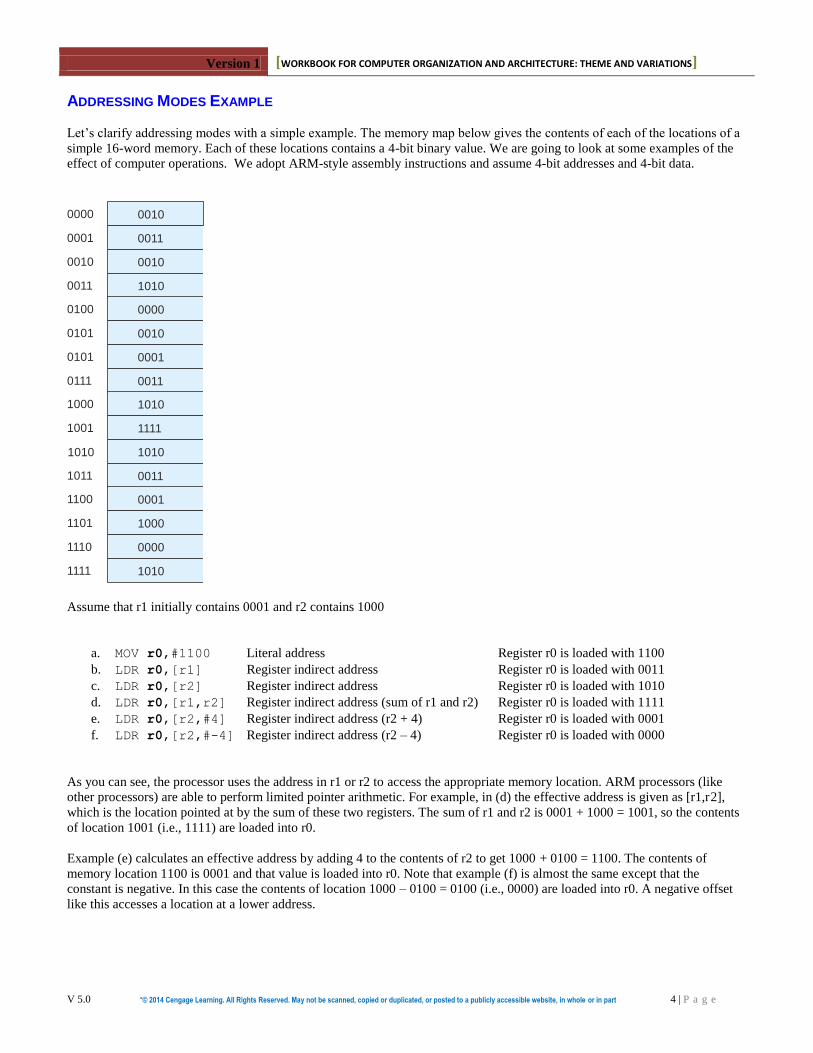
ADDRESSING MODES EXAMPLE
Let’s clarify addressing modes with a simple example. The memory map below gives the contents of each of the locations of a
simple 16-word memory. Each of these locations contains a 4-bit binary value. We are going to look at some examples of the
effect of computer operations. We adopt ARM-style assembly instructions and assume 4-bit addresses and 4-bit data.
Assume that r1 initially contains 0001 and r2 contains 1000
a. MOV r0,#1100 Literal address Register r0 is loaded with 1100
b. LDR r0,[r1] Register indirect address Register r0 is loaded with 0011
c. LDR r0,[r2] Register indirect address Register r0 is loaded with 1010
d. LDR r0,[r1,r2] Register indirect address (sum of r1 and r2) Register r0 is loaded with 1111
e. LDR r0,[r2,#4] Register indirect address (r2 + 4) Register r0 is loaded with 0001
f. LDR r0,[r2,#-4] Register indirect address (r2 – 4) Register r0 is loaded with 0000
As you can see, the processor uses the address in r1 or r2 to access the appropriate memory location. ARM processors (like
other processors) are able to perform limited pointer arithmetic. For example, in (d) the effective address is given as [r1,r2],
which is the location pointed at by the sum of these two registers. The sum of r1 and r2 is 0001 + 1000 = 1001, so the contents
of location 1001 (i.e., 1111) are loaded into r0.
Example (e) calculates an effective address by adding 4 to the contents of r2 to get 1000 + 0100 = 1100. The contents of
memory location 1100 is 0001 and that value is loaded into r0. Note that example (f) is almost the same except that the
constant is negative. In this case the contents of location 1000 – 0100 = 0100 (i.e., 0000) are loaded into r0. A negative offset
like this accesses a location at a lower address.
0000 0010
0001 0011
0010 0010
0011 1010
0100 0000
0101 0010
0101 0001
0111 0011
1000 1010
1001 1111
1010 1010
1011 0011
1100 0001
1101 1000
1110 0000
1111 1010

Version 1 [WORKBOOK FOR COMPUTER ORGANIZATION AND ARCHITECTURE: THEME AND VARIATIONS]
V 5.0 “© 2014 Cengage Learning. All Rights Reserved. May not be scanned, copied or duplicated, or posted to a publicly accessible website, in whole or in part 5 | P a g e
REGISTER TRANSFER LANGUAGE
Before we introduce computer instructions, we are going to define a notation that makes it possible to define instructions
clearly and unambiguously (English language is not a good tool for defining instructions).
Register-transfer language (RTL) is an algebraic notation that describes how information is accessed from memories and
registers and how it is operated on. You should appreciate that RTL is just a notation and not a programming language. RTL
uses square brackets to indicate the contents of a memory location; for example, the expression
[6] = 3
is interpreted as the contents of memory location 6 contains the value 9. If we were using symbolic names, we might write
[Time] = HoursWorked.
If you want to refer to a register, you simply use its name (the names of registers vary from computer to computer – the 68K
has eight data registers called D0, D1, D2, …, D7, whereas the ARM has 16 registers called r0 to r15). So, to say that register
D6 contains the number 123 we write
[D6] = 123
A left or backward arrow indicates the transfer of data. The left-hand side of an expression denotes the destination of the
data defined by the source of the data defined on the right-hand side of the expression. For example, the expression
[MAR] [PC]
indicates that the contents of the program counter, PC, are copied into the memory address register, MAR. The program
counter is the register that holds the location of the next instruction to be executed. The MAR is a register that holds the
address of the next item to be read from memory or written to memory. Note that the contents of the PC are not modified by
this operation.
The operation [3] [5] means copy the contents of memory location 5 to location 3.
EXAMPLE A special-purpose computer has an instruction with a word-length of 24 bits. It is intended to perform operation of the type ADD r3,#24 where ADD is an operation, #24 is a literal (an actual
number), and r3 is a destination register. If there are 200 different instructions and 32 registers, what is the range of unsigned integer literals that can be supported by this computer?
SOLUTION We know that the number of bits used to represent the instruction, plus the number of bits used to select a register, plus the number of bits used to specify a literal must be 24. There are 200 instructions. The next power of 2 greater than this is 256. Since 2
8 = 256, we need 8 bits for the
instruction. There are 32 registers and it requires 5 bits (as 25 = 32) to address a register. Having
allocated 8 bits to the instruction field and 5 bits to the register field, we have 24 – 8 – 5 = 11 bits left over to specify a literal (constant). Consequently, the range of literals that can be handled is 0 to 2047 (as 2
11 = 2048).

Version 1 [WORKBOOK FOR COMPUTER ORGANIZATION AND ARCHITECTURE: THEME AND VARIATIONS]
V 5.0 “© 2014 Cengage Learning. All Rights Reserved. May not be scanned, copied or duplicated, or posted to a publicly accessible website, in whole or in part 6 | P a g e
The operation [3] [5] tells us what's happening at the micro level or register-transfer level. In a high-level language this
operation might be written in the rather more familiar form
x = y;
Consider the RTL expression
[PC] [PC] + 4
which indicates that the number in the PC is increased by 4; that is, the contents of the program counter are read, 4 is added,
and the result is copied into the PC.
Suppose the computer executes an operation that stores the contents of the program counter in location 2000 in the memory.
We can represent this action in RTL as
[2000] [PC].
Occasionally, we wish to refer to the individual bits of a register or memory location. We will do this by means of the subscript
notation (p:q) to mean bits p to q inclusive; for example if we wish to indicate that bits 0 to 7 of a 32-bit register are set to
zero, we write
[R6(0:7)] 0.
Numbers are assumed to be decimal, unless indicated otherwise. Computer languages adopt conventions such as 0x12AC or
$12AC to indicate hexadecimal values. In RTL we will use a subscript; that is 12AC16.
As a final example of RTL notation, consider the following RTL expressions.
a. [20] = 6
b. [20] 6
c. [20] [6]
d. [20] [6] + 3
e. [20] [[2]]
The symbol “”is equivalent to the assignment symbol in high-level languages. Remember that RTL is not a computer
language; it is a notation used to define computer operations.
Example (a) states that memory location 20 contains the value 6. Example (b) states that the number 6 is copied or loaded into
memory location 20. Example (c) indicates that the contents of memory location 6 are copied into memory location 20.
Example (d) reads the contents of location 6, adds 3 to it, and stores the result in location 20. Example (e) is most interesting.
Here, the contents of memory location 2 is read, and that value used to access memory a second time. The new value is loaded
into the contents of memory location 20. This is an example of memory indirect addressing.
Consider the following examples that illustrate the assembly language of four processors and define each instruction in RTL.
Processor family Instruction mnemonic RTL definition
1. 68K MOVE D0,(A5) [[A5]] [D0]
2. ARM ADD r1,r2,r3 [r1] [r2] + [r3]
3. IA32 MOV ah,6 [ah] 6
4. PowerPC li r25,10 [r25] 10

Version 1 [WORKBOOK FOR COMPUTER ORGANIZATION AND ARCHITECTURE: THEME AND VARIATIONS]
V 5.0 “© 2014 Cengage Learning. All Rights Reserved. May not be scanned, copied or duplicated, or posted to a publicly accessible website, in whole or in part 7 | P a g e
QUICK OVERVIEW OF THE ARM Before looking at the ARM processor in detail, we provide a very brief overview. The ARM processor is classified as a 32-bit RISC (reduced instruction set processor) with a three-operand register-to-register instruction set. This is just a fancy way of saying that computer operations involve three operands in registers such as ADD r1,r2,r3. There
are a few instructions that have two operands and some that have four, but that doesn’t change the overall classification. In order to get data into and out of registers (transfers between memory and registers), there are two special instructions called load and store. Load transfers data from memory to a register and store transfers data from a register to memory. These instructions have the forms LDR r0,[r1] and STR r0,[r1]. As we have seen,
these instructions use register indirect (i.e., pointer-based) addressing. The location of the memory element to be accessed is held in a register and the addressing mode indicated by [r1]. The ARM uses a special instruction called ADR (load register with an address) that sets up a pointer in the first place). For example ADR r0,List ;register r0 points at the list
Later, we will explain why this is a special instruction. An ARM instruction like SUB r3,r2,#4 subtracts the actual value 4 (remember that the literal is indicated by the
# symbol) from the contents of register r2 and puts the result in r3. Data operations implemented by ARM processors write the destination (result) operand first on the left. We write the destination operand in bold font to remind you where the result goes. Let’s create a very simple example. MOV r0,#2 ;Put 2 in register r0
MOV r1,#3 ;Put 3 in register r1
ADD r2,r0,r1 ;Add r0 to r1 and put the result in r2
MOV r4,#10 ;Put 10 in r4 (this is where we are going to store the result)
STR r2,[r4] ;Store r2 in memory location 10
Note how simple all this is. You perform one primitive operation at a time.
RTL AND ASSEMBLY LANGUAGE
Don’t confuse RTL and assembly language. An assembly language is a human-readable form of a computer’s binary code. It is designed to be used by programmers and may not always be logical or consistent. Some of you may notice inconsistencies in the assembly language that we learn in this course. RTL is a formal notation that can be manipulated like any algebraic expression. It offers a means of precisely defining operations without using ambiguous English. Consider the RTL example: Suppose that [4] = 3, [10] = 4, and [[10]] = y. We can say that y = 3, because we can substitute y = [[10]] = [4] = 3 Similarly, [[4] + [10] + 6] = [3 + 4 + 6] = [13]

Version 1 [WORKBOOK FOR COMPUTER ORGANIZATION AND ARCHITECTURE: THEME AND VARIATIONS]
V 5.0 “© 2014 Cengage Learning. All Rights Reserved. May not be scanned, copied or duplicated, or posted to a publicly accessible website, in whole or in part 8 | P a g e
QUICK OVERVIEW OF THE 68K Although this text uses the ARM processor family to illustrate an instruction set architecture, we do occasionally refer to the Motorola 68K family. In brief, the Motorola 68K is a 32-bit processor first sold in 1980. The 68K family later became the ColdFire family and is now supported by Freescale because Motorola dropped out of the microprocessor market. The 68K is contemporary with Intel’s IA32. Both the 68K and IA32 have classic register-to-memory architecture. The 68K has a moderately regular instruction set in comparison with the IA32 architecture. Here, the term regular implies that if instruction X has addressing mode Y, then instruction P will also have addressing mode Y. The 68K’s main features are:
A 32-bit architecture with 32-bit registers.
Separate data registers (D0 to D7) and address registers (A0 to A7). Address registers may only be used as pointer registers in generating effective addresses. A register indirect is indicated by (A0).
All registers are 32 bits wide. However, many operations can act on the lower-order 8 bits of a data register, on the lower-order 16 bits, or on the entire 32 bits. The data size is indicated by appending .B, .W, or .L to specify an 8-bit, 16-bit, or 32-bit operation. For example MOVE.B D0,(A0).
Data registers can take part in all data operations. Address registers can take part only in move, add, subtract, and compare operations (that is, MOVA, ADDA, SUBA, CMPA).
Operations on data registers update the CCR register, whereas operations on address registers (apart from compare) do not affect the CCR.
All operations on an address register yield a 32-bit result. You can perform 16-bits additions, subtractions, and loads on an address register, but the result is always sign-extended to 32 bits.
68K instructions are variable length. The shortest instruction is 16-bits. If a single operand is required, the length may be 16+16 or 16+32 bits. The longest instruction is 10 bytes for a move memory location to memory location such as MOVE Data1,Data2.
The addressing modes are: literal (8-, 16-, or 32-bit constant), absolute (actual address of the operand in memory), address register based {(A0), (#offset,A0), (D0,A0)}, predecrementing -(A0), postincrementing (A0)+}
Address register A7 is the system stack pointer and is used to store the return address after a subroutine call. The instruction RTS implements a subroutine return by popping the return address off the top of the stack and loading it in the PC.
Program counter relative addressing is supported. For example, MOVE (PC,#offset),D0.
The creation and deletion of stack fames is supported by LINK (create a frame) and UNLK (delete a frame). A typical fragment of 68K code is: CLR D0 ;clear the total in D0
MOVEA #X,A0 ;A0 points at X
MOVEA #Y,A1 ;A1 points at Y
MOVE #32,D1 ;32 times round the loop
Loop MOVE (A0)+,D2 ;get Xi and increment pointer
MOVE (A1)+,D3 ;get Yi and increment pointer
MULU D2,D3 ;multiply Xi and Yi
ADD D3,D0 ;update running total
SUB #1,D2 ;decrement loop counter
BNE Loop ;Repeat until all done
As you can see, this is not too far from ARM code. The significant difference is the two-operand instruction format.

Version 1 [WORKBOOK FOR COMPUTER ORGANIZATION AND ARCHITECTURE: THEME AND VARIATIONS]
V 5.0 “© 2014 Cengage Learning. All Rights Reserved. May not be scanned, copied or duplicated, or posted to a publicly accessible website, in whole or in part 9 | P a g e
68K INSTRUCTION SET Here’s a summary of the 68K operations. We give the mnemonic, name of the operation, addressing modes, and operand sizes supported (Bytes, Word, Longword). ABCD Add BCD with extend Dx, Dy, -(Ax), -(Ay) B ADD ADD Dn,<ea>, <ea>,Dn BWL ADDA ADD binary to An <ea>,An WL ADDI ADD Immediate #x,<ea>, #<1-8>,<ea> BWL ADDQ ADD 3-bit immediate BWL ADDX ADD eXtended Dy,Dx, -(Ay),-(Ax) BWL AND Bit-wise AND <ea>,Dn, Dn,<ea> BWL ANDI Bit-wise AND with Immediate #<data>,<ea> BWL ASL Arithmetic Shift Left #<1-8>,Dy, Dx,Dy, <ea> BWL ASR Arithmetic Shift Right BWL Bcc Conditional Branch Bcc <label> BW BCHG Test a Bit and CHanGe Dn,<ea> #<data>,<ea> BL BCLR Test a Bit and CLeaR BL BSET Test a Bit and SET BL BSR Branch to SubRoutine BSR <label> BW BTST Bit TeST Dn,<ea> #<data>,<ea> BL CHK CHecK Dn Against Bounds <ea>,Dn W CLR CLeaR <ea> BWL CMP CoMPare <ea>,Dn BWL CMPA CoMPare Address <ea>,An WL CMPI CoMPare Immediate #<data>,<ea> BWL CMPM CoMPare Memory (Ay)+,(Ax)+ BWL DBcc Looping Instruction DBcc Dn,<label> W DIVS DIVide Signed <ea>,Dn W DIVU DIVide Unsigned <ea>,Dn W EOR Exclusive OR Dn,<ea> BWL EORI Exclusive OR Immediate #<data>,<ea> BWL EXG Exchange any two registers Rx,Ry L EXT Sign EXTend Dn WL ILLEGAL ILLEGAL-Instruction Exception JMP JuMP to Affective Address <ea> JSR Jump to SubRoutine <ea> LEA Load Effective Address <ea>,An L LINK Allocate Stack Frame An,#<displacement> LSL Logical Shift Left Dx,Dy #<1-8> ,Dy <ea> BWL LSR Logical Shift Right BWL MOVE Between Effective Addresses <ea>,<ea> BWL MOVE To CCR <ea>,CCR W MOVE To SR <ea>,SR W MOVE From SR SR,<ea> W MOVE USP to/from Address Register USP,An, An,USP <ea>,An L MOVEA MOVE Address WL MOVEM MOVE Multiple <register list>,<ea> <ea>,<register list WL MOVEP MOVE Peripheral Dn,x(An) , x(An),Dn WL MOVEQ MOVE 8-bit immediate #<-128.+127>,Dn L MULS MULtiply Signed <ea>,Dn W MULU MULtiply Unsigned <ea>,Dn W NBCD Negate BCD <ea> B NEG NEGate <ea> BWL NEGX NEGate with eXtend <ea> BWL NOP No OPeration NOT Form one's complement <ea> BWL OR Bit-wise OR <ea>,Dn Dn,<ea> BWL ORI Bit-wise OR with Immediate #<data>,<ea> BWL PEA Push Effective Address <ea> L RESET RESET all external devices ROL ROtate Left #<1-8>,Dy Dx,Dy, <ea> BWL ROR ROtate Right BWL ROXL ROtate Left with eXtend BWL ROXR ROtate Right with eXtend BWL RTE ReTurn from Exception RTR ReTurn and Restore RTS ReTurn from Subroutine SBCD Subtract BCD with eXtend Dx,Dy -(Ax),-(Ay) B Scc Set to -1 if True, 0 if False <ea> B STOP Enable & wait for interrupts #<data> SUB SUBtract binary Dn,<ea> <ea>,Dn BWL SUBA SUBtract binary from An <ea>,An WL SUBI SUBtract Immediate #x,<ea> BWL SUBQ SUBtract 3-bit immediate #<data>,<ea> BWL SUBX SUBtract eXtended Dy,Dx, -(Ay),-(Ax) BWL SWAP SWAP words of Dn Dn W TAS Test & Set MSB & Set N/Z-bits <ea> B TRAP Execute TRAP Exception #<vector> TRAPV TRAPV Exception if V-bit Set TRAPV TST TeST for negative or zero <ea> BWL UNLK Deallocate Stack Frame An

Version 1 [WORKBOOK FOR COMPUTER ORGANIZATION AND ARCHITECTURE: THEME AND VARIATIONS]
V 5.0 “© 2014 Cengage Learning. All Rights Reserved. May not be scanned, copied or duplicated, or posted to a publicly accessible website, in whole or in part 10 | P a g e
THE ARM FAMILY
We use the ARM family in this course to illustrate computer architecture for several reasons. First, it illustrates all the
important elements of an instruction set architecture. Second, it is easy to understand and has a very gentle learning curve in
comparison with some other processors; for example an add operation is specified by ADD r1,r2,r3 which adds register r2
to register r3 and puts the result in r1. What could be simpler? Third, the ARM has some very interesting attributes such as
predicated execution that make it an excellent vehicle for teaching computer architecture.
THE ARM REGISTER SET
The ARM has 16 general-purpose 32-bit data registers, r0 to r15, that can be used by the programmer to store temporary
variables. However, registers r14 and r15 that special purposes. Register r14 holds a subroutine return address after a
subroutine call. Consequently, you should use r14 only to deal with return addresses.
Register r15 holds the program counter, the next instruction to be executed. You cannot use r15 for any other purpose. The
ARM is highly unusual in this respect because all other microprocessor families have a dedicated program counter that is not
normally directly accessible by the programmer. The ARM programmer must not use r15 as a general-purpose data register as
that would crash the computer.
THE INSTRUCTION
Computer instructions are executed sequentially, one by one in turn, unless a special instruction deliberately changes the flow
of control or unless an event called an exception (interrupt) takes place.
The structure of instructions varies from machine to machine. The format of an instruction running on an Intel processor is
different to the format of an instruction running on a 68K or an ARM (even though the instructions might do the same thing).
Instructions are classified by what they do and by the number of operands they take. The three basic instruction types are: data
movement that copies data from one location to another, data processing that operates on data, and flow control that modifies
the order in which instructions are executed. Instruction formats can take zero, one, two, three, or even four operands. Consider
the following examples of instructions with zero to three operands. In these examples operands P, Q, and R may be memory
locations or registers.
Operands Instruction Effect
Three ADD P,Q,R Add R to Q and put the result in P
Two ADD P,Q Add P to Q and put the result in P
One ADD P Add P to an accumulator
Zero ADD Add the top two items on the stack and push the result
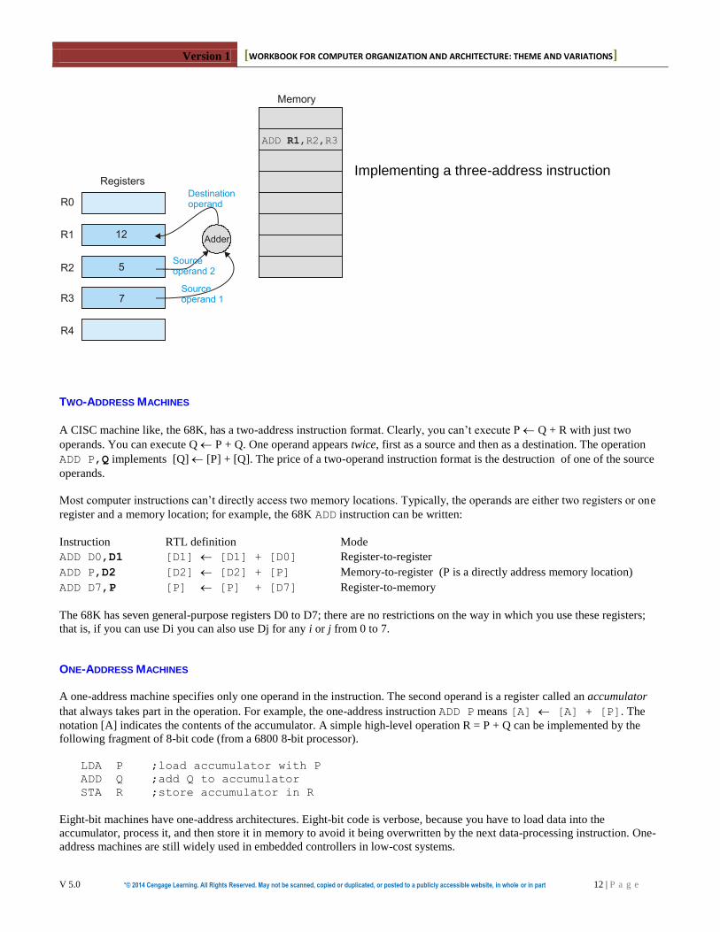
A three-address computer instruction can be written
operation destination,source1,source2
where operation defines the nature of the instruction, source1 is the location of the first operand, source2 is the
location of the second operand, and destination is the location of the result. The instruction ADD r3,r1,r7 adds r1
and r7 to get r3.
This is a little pedantic, but… When we say that r1 is added to r7, we really mean that the contents of r1
is added to the contents of r7. However, it gets boring being so precise so we often just use a register’s
name when we really mean the contents of that register.

Version 1 [WORKBOOK FOR COMPUTER ORGANIZATION AND ARCHITECTURE: THEME AND VARIATIONS]
V 5.0 “© 2014 Cengage Learning. All Rights Reserved. May not be scanned, copied or duplicated, or posted to a publicly accessible website, in whole or in part 11 | P a g e
Microprocessors don’t implement three-address instructions that access memory; you can access only registers. It’s not the
fault of the instruction designer. It’s a limitation imposed by the practicalities of computer technology. Suppose that a computer
has a 32-bit address that allows a total of 232
bytes of memory to be accessed. The three address fields, P, Q, and R needed to
implement ADD P,Q,R would each be 32 bits, requiring 3 × 32 = 96 bits to specify the operands. Assuming a 16-bit operation
code (allowing up to 216
= 65,536 instructions), the total instruction size would be 96 + 16 = 112 bits or 14 bytes. This
instruction format is shown below.
Part (b) of the above figure illustrates a typical RISC instruction format. This uses a register-to-register architecture that allows
three registers to be specified. Each has a 5-bit address field which allows 32 registers.
POSSIBLE THREE-ADDRESS INSTRUCTION FORMATS
Computer technology developed when memory was very expensive indeed. Implementing a 14-byte instruction was not cost-
effective in the 1970s. Even if memory had been cheap, it would have been too expensive to implement 112-bit-wide data
buses to move instructions from point to point in the computer. Finally, main memory is intrinsically slower than on-chip
register.
The modern RISC processor allows you to specify three addresses in an instruction by providing three 5-bit operand address
fields. This restriction lets you select from one of only 32 different operands that are located in registers within the CPU itself.
By using on-chip registers to hold operands, the time taken to access data is minimized because no other storage mechanism
can be accessed as rapidly as a register. An instruction with three 32-bit operands requires 3 × 5 bits to specify the operands
which allows a 32-bit instruction to use the remaining 32 – 15 = 17 bits to specify the instruction.
We’ll use the ADD instruction to add together four values in registers r2, r3, r4, and r5. In the following fragment of code, the
semicolon indicates the start of a comment field that is not part of the executable code. This code is typical of RISC processors
like the ARM.
ADD r1,r2,r3 ;r1 = r2 + r3
ADD r1,r1,r4 ;r1 = r1 + r4
ADD r1,r1,r5 ;r1 = r1 + r5 = r2 + r3 + r4 + r5
Version 1 [WORKBOOK FOR COMPUTER ORGANIZATION AND ARCHITECTURE: THEME AND VARIATIONS]
V 5.0 “© 2014 Cengage Learning. All Rights Reserved. May not be scanned, copied or duplicated, or posted to a publicly accessible website, in whole or in part 12 | P a g e
Implementing a three-address instruction
TWO-ADDRESS MACHINES
A CISC machine like, the 68K, has a two-address instruction format. Clearly, you can’t execute P Q + R with just two
operands. You can execute Q P + Q. One operand appears twice, first as a source and then as a destination. The operation
ADD P,Q implements [Q] [P] + [Q]. The price of a two-operand instruction format is the destruction of one of the source
operands.
Most computer instructions can’t directly access two memory locations. Typically, the operands are either two registers or one
register and a memory location; for example, the 68K ADD instruction can be written:
Instruction RTL definition Mode
ADD D0,D1 [D1] [D1] + [D0] Register-to-register
ADD P,D2 [D2] [D2] + [P] Memory-to-register (P is a directly address memory location)
ADD D7,P [P] [P] + [D7] Register-to-memory
The 68K has seven general-purpose registers D0 to D7; there are no restrictions on the way in which you use these registers;
that is, if you can use Di you can also use Dj for any i or j from 0 to 7.
ONE-ADDRESS MACHINES
A one-address machine specifies only one operand in the instruction. The second operand is a register called an accumulator
that always takes part in the operation. For example, the one-address instruction ADD P means [A] [A] + [P]. The
notation [A] indicates the contents of the accumulator. A simple high-level operation R = P + Q can be implemented by the
following fragment of 8-bit code (from a 6800 8-bit processor).
LDA P ;load accumulator with P
ADD Q ;add Q to accumulator
STA R ;store accumulator in R
Eight-bit machines have one-address architectures. Eight-bit code is verbose, because you have to load data into the
accumulator, process it, and then store it in memory to avoid it being overwritten by the next data-processing instruction. One-
address machines are still widely used in embedded controllers in low-cost systems.

Version 1 [WORKBOOK FOR COMPUTER ORGANIZATION AND ARCHITECTURE: THEME AND VARIATIONS]
V 5.0 “© 2014 Cengage Learning. All Rights Reserved. May not be scanned, copied or duplicated, or posted to a publicly accessible website, in whole or in part 13 | P a g e
SUB-WORD OPERATIONS
If you wish to access individual bytes in a 16- or 32-bit processor, you need special instructions. The 68K family deals with 8-
bit, 16-bit, and 32-bit data by permitting most data-processing instructions to act on an 8-, 16-, or 32-bit slice of a register; for
example ADD.B D0,D1, ADD.W D0,D1 and ADD.L D0,D1 each adds the contents of data register D0 to D1 and puts the
result in D1. The suffix .B specifies an 8-bit byte operation, .W specifies a 16-bit word operation, and .L specifies a 32-bit
longword operation. In each case the bits taking part in the operation are the low-order bits, and bits not taking part in the
operation do not change. For example, the RTL definition of ADD.W D1,D3 is
[D3(0:15)] [D3(0:15)] + [D1(0:15)]
RISC processors do not (generally) support 8- or 16-bit data-processing operations on 32-bit registers, but they do support 8-bit
and 16-bit memory accesses. Consider the following ARM examples.
LDR r0,[r1] ;load r0 with the 32-bit contents of memory pointed at by register r1
LDRB r0,[r1] ;load r0 with the 8-bit contents of memory pointed at by register r1
LDRH r0,[r1] ;load r0 with the 16-bit contents of memory pointed at by register r1
There is also a similar set of store mnemonics with the forms STR, STRB, and STRH.
In 68K terminology 8/16/32 bit values are called byte/word/longword, whereas ARM processor literature uses byte/half
word/word.
DATA SIZE I don’t want to go into the details of data size here because it’s a large topic. However, I do need to introduce a basic concept. If a computer can move data from A to B, or can perform an operation on data, we need to know the number of bits in a word being moved or processed. The very first microprocessor, the Intel 4004, used a 4-bit word because the technology at that time could not economically fabricate chips capable of handling longer wordlengths. The 4004 was able to handle 4-bit values. Very shortly after the introduction of the 4040, 8-bit microprocessors appeared. An 8-bit word is called a byte and operations in 8-bit computers are applied to bytes. You can’t perform a 6-bit operation and you can’t perform a 10-bit operation. Although an 8-bit word can handle text efficiently, it is unsuited to the representation of addresses or to any quantity that can have more than 256 possible values. Eight-bit processors can concatenate two 8-bit words to create a 16-bit address. Over the years, microprocessors grew in complexity to support 16-bit, 32-bit and 64-bit words. The larger the word size, the more work you can do in an instruction. In this course we use ARM processors that have 32-bit data words and 32-bit addresses. However, just as 4-bit and 8-bit words are too short to represent many types of data, 32-bit and 64-bit words are often too big. For example, if you use ASCII-encoded text, each character requires 8 bits. If you put an ASCII character in a 32-bit register, 24 bits are unused. This represents an inefficient use of storage. So, programmers often employ tricks to pack more than one character in a word.

Version 1 [WORKBOOK FOR COMPUTER ORGANIZATION AND ARCHITECTURE: THEME AND VARIATIONS]
V 5.0 “© 2014 Cengage Learning. All Rights Reserved. May not be scanned, copied or duplicated, or posted to a publicly accessible website, in whole or in part 14 | P a g e
Suppose a processor supports operations that act on a subsection of a register. What happens to the bits that do not take part in
the operation? Assume that a register is partitioned as figure (a) demonstrates.
Figure (b) shows how some processors deal with the problem by ignoring higher-order bits. If you add the two-low-order bytes
in a 32-bit word, bits 0 to 7 are added together and bits 8 to 31 remain unchanged; for example, 0x12345678 + 0x11111111 =
0x12345689. This is true of the 68K processor.
Figure (c) demonstrates an alternative arrangement. Here, the bits not taking part in an operation are automatically cleared. In
this case, 0x12345678 + 0x11111111 = 0x00000089.
In (d) the bits not taking part in an operation are sign-extended. This means that if you add two bytes in a 32-bit word, the
result is sign extended to 32 bits. The 68K treats the contents of address registers in this way. If you perform a 16-bit operation
on an address register, the result is sigh-extended to 32 bits.
PROBLEM SET 3
These questions ask you about the role of registers in computer architecture, the role of addressing modes, and the design of
computer instruction sets.
1. In the context of microprocessors, what is a user-visible register?
2. Modern microprocessors have more registers than previous generations of microprocessors. Why?
3. Registers are used in different ways by different microprocessor families (e.g., Intel IA32, Motorola 68K, ARM etc.).
Describe some of the differences in the way in which registers are used and comment on the relative merits.
4. A special-purpose computer’s instruction set is 24 bytes wide. This is a three-operand load and store (register-to-register)
machine. If this computer provides 64 general-purpose registers, how many different instructions can be implemented?
5. A 32-bit computer with a 32-bit instruction word uses 122 different instructions. If this computer has a three-address
register-to-register instruction set, how many registers can be supported?
6. A computer devotes only 4 bits in its instruction word to the selection of one of 16 registers. Can you suggest of ways of
providing more than 16 registers while keeping the number of bits in an instruction that selects a register at 4?
Version 1 [WORKBOOK FOR COMPUTER ORGANIZATION AND ARCHITECTURE: THEME AND VARIATIONS]
V 5.0 “© 2014 Cengage Learning. All Rights Reserved. May not be scanned, copied or duplicated, or posted to a publicly accessible website, in whole or in part 15 | P a g e
7. What are the various groups of instruction types implemented by typical microprocessors (i.e., how are instructions
classified)? Give examples of different types of instructions.
8. What are the relative merits of one-address, two-address, and three-address instructions?
9. Under what circumstances is it possible to have a zero-address computer?
10. Are there occasions where 4-address or even 5-address instructions could prove useful?
USING THE KEIL SIMULATOR
The processor in the PC is not a member of the ARM family. It’s usually a member of Intel’s IA32 family or an AMD
processor. However, you can run ARM code processor on your PC using a program from KeilTM
. This can be found at
www.keil.com. The Keil package, called µVision4, is very sophisticated and is intended for engineers designing embedded
ARM-based systems. Consequently,it includes far more facilities than we need. The demonstration version that you can
download for a PC is limited to assembly-level programs smaller than 32K bytes. This restriction is not be a problem for
students.
Essentially, µVision4 is an IDE (integrated development system) that is project-based; that is, each new program must be part
of a project. You begin by creating a project (i.e., a container for all your files) and then select the target processor you are
going to use. You create source files (in our case, these will be assembly language files) and then you build your application
(i.e., create code for your chosen processor). µVision4 allows you to construct projects with multiple source files and files in C
or C++, although we will not be using these facilities. Having built your file, you can execute it and follow the progress of its
execution.
Let’s step through the process of creating a program. Note that this package will continue to be upgraded during its life and
there may be differences between these examples and the system you are using. However, the sequence of operations should
remain substantially the same. On loading µVision4 you are presented with the following screen.
To start, select Project from the upper row of tabs and then New µVision Project from the pull-down window. This brings up
the Create New Project Window and you create a project name in the selected directory. I will use FirstExample. The
development system automatically appends a file type to create FirstExample.uvproj.
When you hit save, a new window will automatically appear that invites you to select the device you are going to use. In this
case it is the ARM (see the figure below). If you select the ARM pull-down window, it will offer various ARM versions. I used
the ARM7 (Big Endian) version. Once you have elected the processor, a return is made to the basic project window.

Version 1 [WORKBOOK FOR COMPUTER ORGANIZATION AND ARCHITECTURE: THEME AND VARIATIONS]
V 5.0 “© 2014 Cengage Learning. All Rights Reserved. May not be scanned, copied or duplicated, or posted to a publicly accessible website, in whole or in part 16 | P a g e
Selecting the target device
The next step is to create a source file. Click File in the main window. This will open a file window with the default name
Text1. Now you can enter you source program.
After entering the program you need to save it. This is done in the normal Windows way: select file and then save. You then
have to give it a name. I chose FirstExample.asm. Note that I used the extension .asm (assembly langue) because the
development system does not know which type of source file you are creating. The following image shows the screen after the
program has been entered and saved.
This program is simple. It loads register with numbers (literals), adds them together and then moves the result into register r0.
Note that there are three lines that are not part of the assembly language. These are assembler directives that tell the assembler
things it needs to know. The first assemble directive is
AREA FirstExample, CODE, READONLY
Choose the processor
you wish to simulate
from this list.
Assembler directives

Version 1 [WORKBOOK FOR COMPUTER ORGANIZATION AND ARCHITECTURE: THEME AND VARIATIONS]
V 5.0 “© 2014 Cengage Learning. All Rights Reserved. May not be scanned, copied or duplicated, or posted to a publicly accessible website, in whole or in part 17 | P a g e
The purpose of this AREA directive is to name the region of memory where the program will be located. In this case we’ve
used FirstExample. The parameter CODE indicates that the data will be code rather than data. The third parameter
READONLY indicates that the memory is read-only becausewe are not going to alter its contents.
The ENTRY directive simply tells the assembler that the code is to be executed from this point. It’s the starting point.
The final directive, END, indicates the end of the program and that there is no further code beyond this point.
The next step is to tell the project manager about the assembly file we’ve just created. Click on Project to select the project
drop-down menu and then select Manage. Then select Components, Environment, Books... from the secondary drop-down
window. The figure (below left) shows this situation. Now click Add Files to select your source file. You will have to change
the File of Type box from its default C Source file (*.C) to ASM Source file. Having done that, you should have the situation
below right with one file displayed. Then click OK to end the sequence.
At this stage, we have a project, a processor, and a source file. Now we need to create the environment and assemble the code.
Click on Project and then Build target from the drop-down window. The following image shows the screen after we have
built the target.
The source file we
created.
Note how the assembler has
formatted your code. It uses
color to distinguish between
code and comments and it
highlights literals.
Version 1 [WORKBOOK FOR COMPUTER ORGANIZATION AND ARCHITECTURE: THEME AND VARIATIONS]
V 5.0 “© 2014 Cengage Learning. All Rights Reserved. May not be scanned, copied or duplicated, or posted to a publicly accessible website, in whole or in part 18 | P a g e
The Build Output window shows the status of the process. Here we are interested only in the magic words 0 Error(s) that
indicate all went well. Had there been any errors in the code, we would have been informed and would have had to edit the
source file and then rebuild it. This cycle is repeated until there are no errors reported.
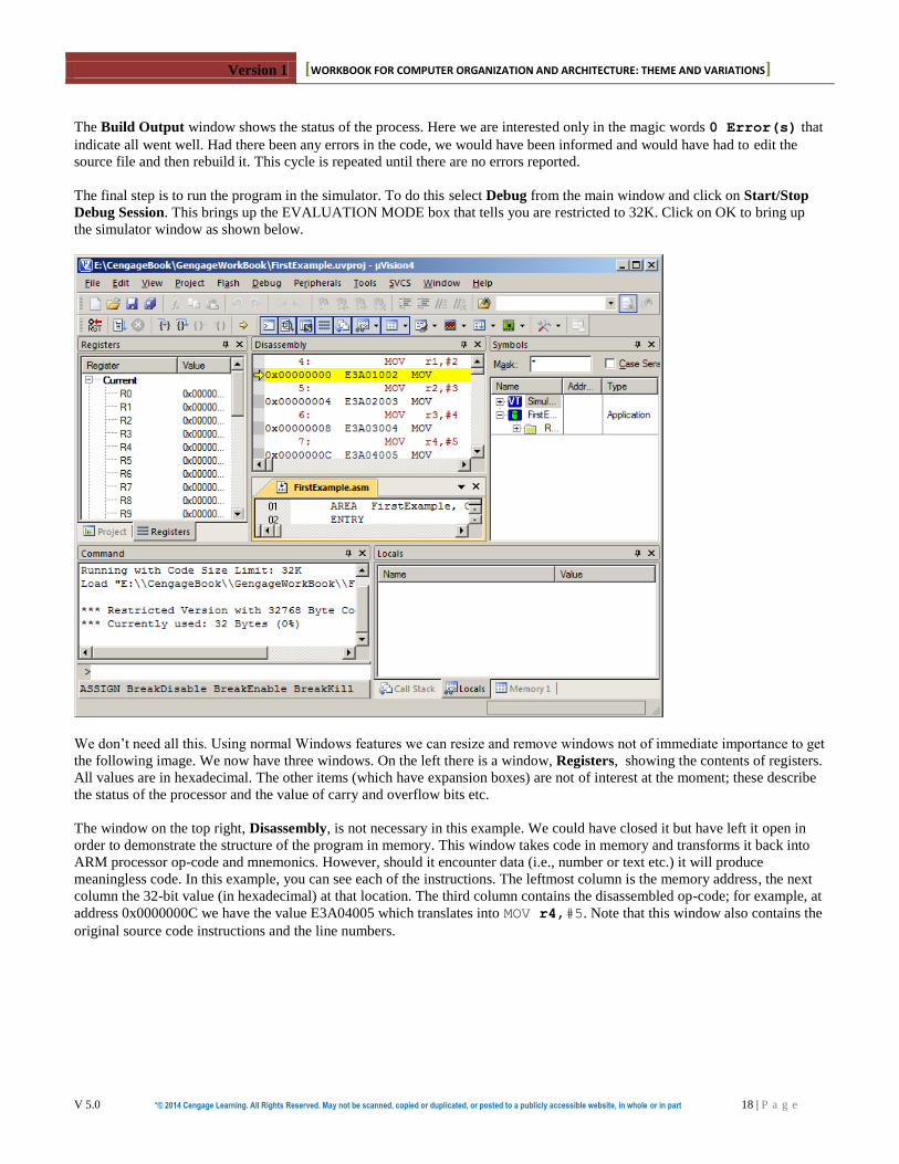
The final step is to run the program in the simulator. To do this select Debug from the main window and click on Start/Stop
Debug Session. This brings up the EVALUATION MODE box that tells you are restricted to 32K. Click on OK to bring up
the simulator window as shown below.
We don’t need all this. Using normal Windows features we can resize and remove windows not of immediate importance to get
the following image. We now have three windows. On the left there is a window, Registers, showing the contents of registers.
All values are in hexadecimal. The other items (which have expansion boxes) are not of interest at the moment; these describe
the status of the processor and the value of carry and overflow bits etc.
The window on the top right, Disassembly, is not necessary in this example. We could have closed it but have left it open in
order to demonstrate the structure of the program in memory. This window takes code in memory and transforms it back into
ARM processor op-code and mnemonics. However, should it encounter data (i.e., number or text etc.) it will produce
meaningless code. In this example, you can see each of the instructions. The leftmost column is the memory address, the next
column the 32-bit value (in hexadecimal) at that location. The third column contains the disassembled op-code; for example, at
address 0x0000000C we have the value E3A04005 which translates into MOV r4,#5. Note that this window also contains the
original source code instructions and the line numbers.

Version 1 [WORKBOOK FOR COMPUTER ORGANIZATION AND ARCHITECTURE: THEME AND VARIATIONS]
V 5.0 “© 2014 Cengage Learning. All Rights Reserved. May not be scanned, copied or duplicated, or posted to a publicly accessible website, in whole or in part 19 | P a g e
The window below is the same as above except that we’ve closed the disassembly window and resized to reduce clutter.

Version 1 [WORKBOOK FOR COMPUTER ORGANIZATION AND ARCHITECTURE: THEME AND VARIATIONS]
V 5.0 “© 2014 Cengage Learning. All Rights Reserved. May not be scanned, copied or duplicated, or posted to a publicly accessible website, in whole or in part 20 | P a g e
The final step is to run the code. We can run it in several different ways. Here, we are going to execute it line by line so that we
can observe the way in which the contents of the registers change after each instruction. In the image below, we have clicked
on the step one line icon (highlighted in the image) and the first instruction has been executed. Note that in the register list, r1
is highlighted and it has the value 2 (because it was loaded with 2). The contents of the program counter, r15, are 4 because it
now points to the second instruction.
The next image shows the screen after we have clicked the step-in button five times and have executed the first five
instructions.
Note that you have to click on Debug and then Start/stop Debugging Session to get out of the debug mode.
This is the step-in icon. Click
on it and one instruction is
executed.
Note that executing the first
instruction has loaded r1 with 2
(i.e., 0x00000002)
This is the situation after the ADD r1,r1,r2
has been executed. Register r1 initially contains 2
and r2 contains 3. After the addition r1 contains
2+3 = 5.

Version 1 [WORKBOOK FOR COMPUTER ORGANIZATION AND ARCHITECTURE: THEME AND VARIATIONS]
V 5.0 “© 2014 Cengage Learning. All Rights Reserved. May not be scanned, copied or duplicated, or posted to a publicly accessible website, in whole or in part 21 | P a g e
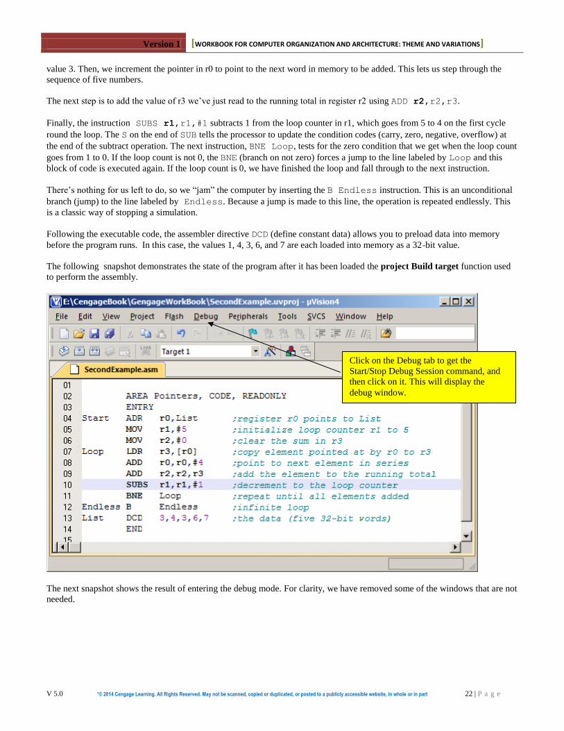
USING THE KEIL SIMULATOR: A SECOND EXAMPLE
Let’s now look at a more realistic example of the use of the simulator that includes both a loop and an example register indirect
addressing. We are going to add together five numbers stored in memory.
AREA Pointers, CODE, READONLY
ENTRY
Start ADR r0,List ;register r0 points to List
MOV r1,#5 ;initialize loop counter in r1 to 5
MOV r2,#0 ;clear the sum in r3
Loop LDR r3,[r0] ;copy the element pointed at by r0 to r3
ADD r0,r0,#4 ;point to the next element in the series
ADD r2,r2,r3 ;add the element to the running total
SUBS r1,r1,#1 ;decrement to the loop counter
BNE Loop ;repeat until all elements added
Endless B Endless ;infinite loop
List DCD 3,4,3,6,7 ;the data (five 32-bit words)
END
The executable code consists of three parts. The first part beginning with the label Start sets up the environment. The
instruction ADR r0,List is a pseudo instruction that loads the 32-bit value of List into register r0. List is a label that
refers to the five items of data in memory. What is the value of List? That’s something the programmer doesn’t have to
worry about; the assembler’s job is to convert labels into their actual values. However, in this case it is easy. The assembler
begins at address zero and each instruction occupies four bytes. The code consists of eight instructions which occupy 8 × 4 =
32 bytes. Consequently List refers to location 0x00000020.
The two move instructions initialize a loop counter (we are going to go round five times), and set the initial total to zero.
The body of the code which we’ve printed in blue performs the actual addition. The LDR r3,[r0] instruction loads register
r3 with the contents of the memory location pointed at by r0. Since we initialized r0 to point to List, we will first access the
A COMMENT ON PROGRAM LAYOUT When writing an assembly language program, column one is reserved for a user-defined name that allows us to refer to that line (more specifically, it corresponds to the address of that line in the program when it’s been assembled into machine code). In this example, the four labels are Start, Loop, Endless, and List. Actually, Start, is a dummy label in the sense we never refer to it. I added it simply to demonstrate that we can label a line just for the programmer (this indicates the start of the program). Anywhere after column one, we can write an instruction. The only rule is that there must be at least one space following the mnemonic, and that parameters must be separated by commas. Spaces after a comma are optional; for example, we can write ADD r1,r2,r3 or
ADD r1, r2, r3
Finally, we can append a comment to the right. The assembler we are using requires a semicolon to separate it from the code. Although we don’t have to write a program in columns as we’ve done above, it makes the program easier to read.
Version 1 [WORKBOOK FOR COMPUTER ORGANIZATION AND ARCHITECTURE: THEME AND VARIATIONS]
V 5.0 “© 2014 Cengage Learning. All Rights Reserved. May not be scanned, copied or duplicated, or posted to a publicly accessible website, in whole or in part 22 | P a g e
value 3. Then, we increment the pointer in r0 to point to the next word in memory to be added. This lets us step through the
sequence of five numbers.
The next step is to add the value of r3 we’ve just read to the running total in register r2 using ADD r2,r2,r3.
Finally, the instruction SUBS r1,r1,#1 subtracts 1 from the loop counter in r1, which goes from 5 to 4 on the first cycle
round the loop. The S on the end of SUB tells the processor to update the condition codes (carry, zero, negative, overflow) at
the end of the subtract operation. The next instruction, BNE Loop, tests for the zero condition that we get when the loop count
goes from 1 to 0. If the loop count is not 0, the BNE (branch on not zero) forces a jump to the line labeled by Loop and this
block of code is executed again. If the loop count is 0, we have finished the loop and fall through to the next instruction.
There’s nothing for us left to do, so we “jam” the computer by inserting the B Endless instruction. This is an unconditional
branch (jump) to the line labeled by Endless. Because a jump is made to this line, the operation is repeated endlessly. This
is a classic way of stopping a simulation.
Following the executable code, the assembler directive DCD (define constant data) allows you to preload data into memory
before the program runs. In this case, the values 1, 4, 3, 6, and 7 are each loaded into memory as a 32-bit value.
The following snapshot demonstrates the state of the program after it has been loaded the project Build target function used
to perform the assembly.
The next snapshot shows the result of entering the debug mode. For clarity, we have removed some of the windows that are not
needed.
Click on the Debug tab to get the
Start/Stop Debug Session command, and
then click on it. This will display the
debug window.

Version 1 [WORKBOOK FOR COMPUTER ORGANIZATION AND ARCHITECTURE: THEME AND VARIATIONS]
V 5.0 “© 2014 Cengage Learning. All Rights Reserved. May not be scanned, copied or duplicated, or posted to a publicly accessible website, in whole or in part 23 | P a g e
There are two notable features. First, the pseudo operation ADR r0,List has been translated into the actual instruction
ADD r0,PC,#0x0000001C. A pseudo operation uses existing instruction to create an operation that loads a 32-bit value
into a register. The assembler might generate different code on different occasions.
A second interesting feature also appears in the disassembly window. You can easily recognize the program in this window.
However, the data values stored by the assembler in memory (i.e., 5, 5, 6, 7) are read by the disassembler and translated into
instructions. In this case the first value, 5, corresponds to the code for ANDEQ r0,r0,r3). Of course, this code is nonsense.
However, the disassembler does not know this; it just translates anything in memory into an instruction.
Disassembled
code window.
Some of the
debugging
commands.
Instruction generated by the
pseudo operation ADR r0,List.
The constants
created by DCD.
Version 1 [WORKBOOK FOR COMPUTER ORGANIZATION AND ARCHITECTURE: THEME AND VARIATIONS]
V 5.0 “© 2014 Cengage Learning. All Rights Reserved. May not be scanned, copied or duplicated, or posted to a publicly accessible website, in whole or in part 24 | P a g e
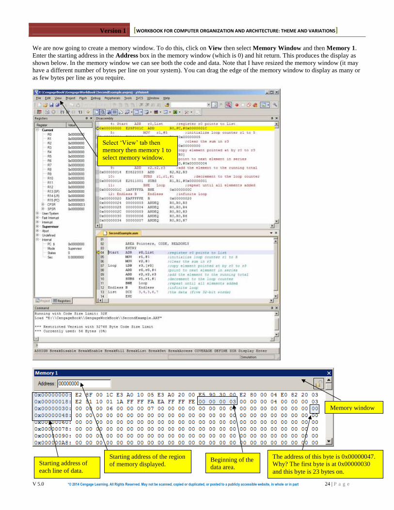
We are now going to create a memory window. To do this, click on View then select Memory Window and then Memory 1.
Enter the starting address in the Address box in the memory window (which is 0) and hit return. This produces the display as
shown below. In the memory window we can see both the code and data. Note that I have resized the memory window (it may
have a different number of bytes per line on your system). You can drag the edge of the memory window to display as many or
as few bytes per line as you require.
Memory window
Select ‘View’ tab then
memory then memory 1 to
select memory window.
Starting address of the region
of memory displayed. Beginning of the
data area. Starting address of
each line of data.
The address of this byte is 0x00000047.
Why? The first byte is at 0x00000030
and this byte is 23 bytes on.

Version 1 [WORKBOOK FOR COMPUTER ORGANIZATION AND ARCHITECTURE: THEME AND VARIATIONS]
V 5.0 “© 2014 Cengage Learning. All Rights Reserved. May not be scanned, copied or duplicated, or posted to a publicly accessible website, in whole or in part 25 | P a g e
Let’s now run through a debug session with this program. The snapshot below shows the screen after we have executed the
first three instructions. You can see that r0 is loaded with 0x24 (the start of the data area), r1 contains 5, and r2 contains 0
(note, we have to clear r2 to 0 in the code because, in a real system, r2 will probably not contain 0 at the start of a block of
code). Failure to initialize registers is proably the most common error that students make when writing assembly language
programms.
The next instruction to be executed is highlighted in both the program and disassembly windows.
The next snapshot shows the state of the simulator after we have nearly completed one trip round the loop and are at the last
instruction, the branch to Loop on not zero. The value of r0 is 28 (i.e., 24 + 4) because we are pointing at the next data item.
The value of r1 (the loop counter) is 4 because we’ve decremented it on this trip. The value of r3 is 3 because we’ve loaded the
first number, and the value of r2 is three because the sum contains only one number so far.
The final snapshot for this example just shows some of the registers and code. Rregister r2 now holds the sum of the five
numbers in memory. The value of r0 contains 0x38 which the next location after the five numbers (24 + 5 × 4 = 38 using
hexadecimal arithmetic).

Version 1 [WORKBOOK FOR COMPUTER ORGANIZATION AND ARCHITECTURE: THEME AND VARIATIONS]
V 5.0 “© 2014 Cengage Learning. All Rights Reserved. May not be scanned, copied or duplicated, or posted to a publicly accessible website, in whole or in part 26 | P a g e
The sum of the five elements is in
register r2. This is 0x00000017 or
23 decimal. The five elements are
3,4,3,6,7 and their sum is indeed 23.

Version 1 [WORKBOOK FOR COMPUTER ORGANIZATION AND ARCHITECTURE: THEME AND VARIATIONS]
V 5.0 “© 2014 Cengage Learning. All Rights Reserved. May not be scanned, copied or duplicated, or posted to a publicly accessible website, in whole or in part 27 | P a g e
Let’s look another program that uses pointer-based addressing to access memory. The snapshot below illustrates a program that
adds together pairs of elements of two vectors X and Y, and puts the result in Z; that is, it performs zi = xi + yi for i = 0 to 3.
We’ve defined two data areas: AREA VectorAddition, CODE, READONLY where the program code is located, and
AREA VectorAddition, DATA, READWRITE. The parameters CODE and DATA refer to regions of memory that
contain code or data, and the parameters READONLY and READWRITE indicate that the region of memory space can only be
read (as in the case of the program), or can be both read from or written to (using parameter READWRITE).
Once the program is ready to run, you select Debug and Start/Stop Debug Session in the normal way. We then have to
perform an additional step to indicate that the data memory is writable. Click the Debug tab and then the Memory Map tab.
The Memory Map below shows the situation with the address range 0x00 to 0x5B defined as both executable and readable
memory. We need to define locations 0x38 to 0x5B as writable locations. To do this, enter the values in the Map Range box
and tick Read and Write.
The image on the left shows the Memory Map box after
we’ve entered the read/write range. Now click the
Close tag.

Version 1 [WORKBOOK FOR COMPUTER ORGANIZATION AND ARCHITECTURE: THEME AND VARIATIONS]
V 5.0 “© 2014 Cengage Learning. All Rights Reserved. May not be scanned, copied or duplicated, or posted to a publicly accessible website, in whole or in part 28 | P a g e
The final three snapshots for this example show, in order, the initial memory map, the state of the system during execution,
and the final memory map.
The initial memory map shows the code from 0x00000000 to 0x0000001B, and the data area starting at 0x0000002C. The
snapshot is taken at the end of the first cycle of iteration. The three pointer registers are loaded with addresses that are four
bytes greater than the start of the three vectors, because auto-incrementing is used and the pointer is increased after it has been
used. The final memory map shows the source data in read and the data written back to memory in green.
Version 1 [WORKBOOK FOR COMPUTER ORGANIZATION AND ARCHITECTURE: THEME AND VARIATIONS]
V 5.0 “© 2014 Cengage Learning. All Rights Reserved. May not be scanned, copied or duplicated, or posted to a publicly accessible website, in whole or in part 29 | P a g e
PROBLEM SET 4 1. What is an assembler?
2. What is a cross-assembler?
3. What is a (CPU) simulator?
4. Does a simulator run as fast as the native or target processor being simulated? For example, does ARM processor
code being executed by a simulated ARM processor on a PC run faster or slower than the same code being run on a
real ARM processor?
5. What is the wrong with ADD r0,r16,r1?
6. Is there anything wrong with ADD r0,r0,r0?
7. Why is ADD r1,#5,r2 wrong?
8. What is the difference between a syntax error and a semantic error?
9. What is the difference between an instruction and an assembler directive?
10. What is the effect of ADR r0,1234?
11. ADR r0,#1234 is known as a pseudo instruction. What is a pseudo instruction and what is its purpose?
12. What’s wrong, if anything, with ADD r15,r2,r3?
PROBLEM SET 5
Here we provide an introduction to the Keil ARM processor development system.
1. Write a simple program to perform: Z = A + B + C – (D × E)
The instructions you may use are ADD, SUB, and MUL. Assume that the data is in registers r0 to r4 (representing A to
E) and the result is put in r5.
Enter your program into the Keil simulator and run it. You can use move instruction to load data into registers. Do you
get the expected answer?
2. Now assume A, B, C, D and E are 16-bit values in memory. You can load them by using a DCD directive. Remember
that you use a label to define the first memory location and you can put successive values on the same line by
separating them by commas. However, since each data item needs its own name, you are going to have to use one
directive per element; that is:,
A DCD 4
B DCD 12
C DCD -2
Enter the program, compile (build) it and test it.
3. Write a program that includes deliberate syntax errors. Enter it in the development system, assemble (build) it and
then debug it.

Version 1 [WORKBOOK FOR COMPUTER ORGANIZATION AND ARCHITECTURE: THEME AND VARIATIONS]
V 5.0 “© 2014 Cengage Learning. All Rights Reserved. May not be scanned, copied or duplicated, or posted to a publicly accessible website, in whole or in part 30 | P a g e
POINTER-BASED ADDRESSING MODES
We have already introduced addressing modes. Here we discuss the ARM processor’s register indirect
addressing mode that supports several variations. This is an important topic because it’s essential to the
efficient manipulation of data structures such as tables, arrays, matrixes, and vectors.
Let’s first review the basic concept of register indirect, or pointer-based, addressing. Indirect addressing specifies a pointer to
the actual operand which is invariably in a register. For example, the instruction, LDR r0,[r1], first reads the contents of
register r1 to obtain the pointer that gives you the address of the actual operand in memory. It then reads the memory location
specified by the pointer in r1 to get the required data. This addressing mode requires three memory accesses; the first is to read
the instruction to identify the register containing the pointer, the second is to read the contents of the register to get the pointer.
And the third is to get the desired operand at the location specified by the pointer.
You can easily see why this addressing mode is called indirect because the address register specifies the operand indirectly by
telling you where it is, rather than what it is. This is the only form of addressing that the ARM processor can use to access
memory. The box below describes three variations on this addressing mode and gives their assembly language forms, defines
the addressing mode (using RTL), and gives them names. The naming of addressing modes is not always consistent in
computer science and manufacturers sometimes use different names for the same addressing mode.
ARM PROCESSOR POINTER-BASED ADDRESSING MODES
1. LDR r1,[r0] r0 points at the operand
[r1] ← [[r0]]
Base register addressing
2. LDR r1,[r0,#4] The operand is 4 bytes on from the location pointed at by r0
[r1] ← [[r0 + 4]]
Pre-indexed addressing
3. LDR r1,[r0,#4]! The operand is 4 bytes on from the location pointed at by r0. After loading
the operand, the pointer register is incremented by 4
[r1] ← [[r0 + 4]]
[r0] ← [r0 ] + 4
Pre-indexed addressing with writeback
Autoincrementing preindexed addressing
4. LDR r1,[r0],#4 The operand is pointed at by r0. After making the access, r0 is updated by 4.
[r1] ← [[r0]]
[r0] ← [r0 ] + 4
Post-indexed addressing

Version 1 [WORKBOOK FOR COMPUTER ORGANIZATION AND ARCHITECTURE: THEME AND VARIATIONS]
V 5.0 “© 2014 Cengage Learning. All Rights Reserved. May not be scanned, copied or duplicated, or posted to a publicly accessible website, in whole or in part 31 | P a g e
The following figure describes the basic register indirect (sometimes called indexed or base addressing). The instruction
specifies an address register and that register points at the actual location of the data in memory.
This diagram demonstrates the effect of
incrementing r0 by 4. Now, r0 points at the next
word so that executing LDR r1,[r0] accesses a
different location; that is, the same instruction has
a different outcome.
PLAYING WITH POINTERS
In principle, you don’t need any addressing mode other than the simple register indirect [r0]. In practice, computer design is
very much about the tradeoff between computational efficiency, complexity, and cost. Most computers provide variations on
the basic register indirect addressing mode in order to reduce the size of the code and speed up its execution. In the 1980s, this
was taken to extremes by the 68020 microprocessor that had truly complex addressing modes that could perform amazing
operations with a single instruction. However, such addressing modes were so complex that compilers could not handle them
optimally, and they took up a big chunk of the silicon chip. They were, at best, used infrequently. And they were slow.
Consider the operation LDR r1,[r0,#8].
This is only a slight modification of ARM’s plain
vanilla register indirect addressing. The
difference is the literal within the square
brackets. The address of the operand is found at
[r0] + 8; that is, the operand is 8 bytes on from
the location pointer at by r0. This addressing
mode is sometimes called pre-indexed
addressing.
The offset, in this case 8, is not added to the
contents of the pointer in the register. The
contents of r0 are fed to an adder, the offset
added, and the result used to access memory. The contents of register r0 do not change.
A typical application of pre-indexed addressing is in accessing a table. Consider a table in memory containing 12 entries
corresponding to January to December. Register r0 points at the start of the table (i.e., January). The following operations have
the effect:
Accumulator
Memory
r0Pointer register
n
n+4
n+8
n-4
Destination
r1
n
8
The operand loaded into r1 is 8 bytes from the location pointed at by r0.
Executing LDR r1,[r0,#8]
Version 1 [WORKBOOK FOR COMPUTER ORGANIZATION AND ARCHITECTURE: THEME AND VARIATIONS]
V 5.0 “© 2014 Cengage Learning. All Rights Reserved. May not be scanned, copied or duplicated, or posted to a publicly accessible website, in whole or in part 32 | P a g e
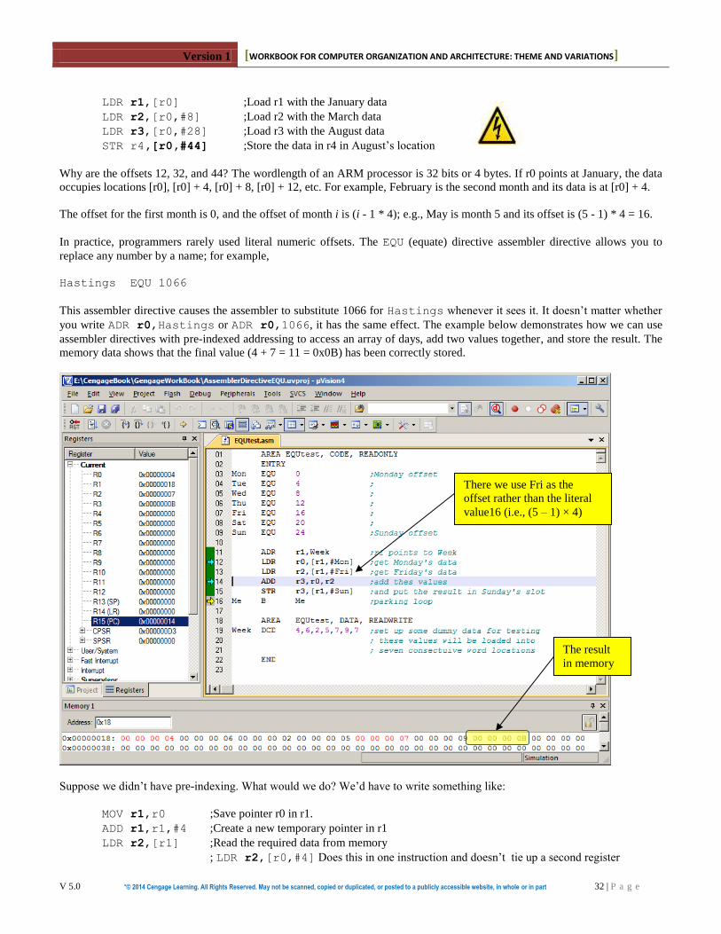
LDR r1,[r0] ;Load r1 with the January data
LDR r2,[r0,#8] ;Load r2 with the March data
LDR r3,[r0,#28] ;Load r3 with the August data
STR r4,[r0,#44] ;Store the data in r4 in August’s location
Why are the offsets 12, 32, and 44? The wordlength of an ARM processor is 32 bits or 4 bytes. If r0 points at January, the data
occupies locations [r0], [r0] + 4, [r0] + 8, [r0] + 12, etc. For example, February is the second month and its data is at [r0] + 4.
The offset for the first month is 0, and the offset of month i is (i - 1 * 4); e.g., May is month 5 and its offset is (5 - 1) * 4 = 16.
In practice, programmers rarely used literal numeric offsets. The EQU (equate) directive assembler directive allows you to
replace any number by a name; for example,
Hastings EQU 1066
This assembler directive causes the assembler to substitute 1066 for Hastings whenever it sees it. It doesn’t matter whether
you write ADR r0,Hastings or ADR r0,1066, it has the same effect. The example below demonstrates how we can use
assembler directives with pre-indexed addressing to access an array of days, add two values together, and store the result. The
memory data shows that the final value (4 + 7 = 11 = 0x0B) has been correctly stored.
Suppose we didn’t have pre-indexing. What would we do? We’d have to write something like:
MOV r1,r0 ;Save pointer r0 in r1.
ADD r1,r1,#4 ;Create a new temporary pointer in r1
LDR r2,[r1] ;Read the required data from memory
; LDR r2,[r0,#4] Does this in one instruction and doesn’t tie up a second register
The result
in memory
There we use Fri as the
offset rather than the literal
value16 (i.e., (5 – 1) × 4)

Version 1 [WORKBOOK FOR COMPUTER ORGANIZATION AND ARCHITECTURE: THEME AND VARIATIONS]
V 5.0 “© 2014 Cengage Learning. All Rights Reserved. May not be scanned, copied or duplicated, or posted to a publicly accessible website, in whole or in part 33 | P a g e
Simple pre-indexing is useful for accessing elements at a specified offset. However, it does not change the pointer. Sometimes,
we are stepping through a data structure and we need to permanently update the pointer each time it’s used; for example:
MOV r2,#64 ;Set up loop count for 64 elements
MOV r3,#0 ;Clear the sum
ADR r0,Table ;Point to the table of data elements to be summed
Next LDR r1,[r0] ;Repeat: Read an element
ADD r0,r0,#4 ; Update the pointer
ADD r3,r3,r1 ; Add a new element to the total
SUBS r2,r2,#1 ; Decrement loop counter
BNE Next ;Repeat until all done
There’s nothing new here. After accessing an element we update the pointer ready for the next cycle of iteration (in blue).
Fortunately, ARM processors provide a post-indexed addressing mode. The offset is provided after the pointer, as the example
demonstrates.
LDR r1,[r0],#4
In this case, the operand is accessed at the address pointer at by r0, and then r0 is incremented by 4. This addressing mode
saves an instruction without incurring a time penalty. We can now write.
MOV r2,#64 ;Set up loop count for 64 elements
MOV r3,#0 ;Clear the sum
ADR r0,Table ;Point to the table of data elements to be summed
Next LDR r1,[r0],#4 ;Repeat: Read an element and update the pointer
ADD r3,r3,r1 ; Add a new element to the total
SUBS r2,r2,#1 ; Decrement loop counter
BNE Next ;Repeat until all done
Version 1 [WORKBOOK FOR COMPUTER ORGANIZATION AND ARCHITECTURE: THEME AND VARIATIONS]
V 5.0 “© 2014 Cengage Learning. All Rights Reserved. May not be scanned, copied or duplicated, or posted to a publicly accessible website, in whole or in part 34 | P a g e
OVERVIEW OF THE ARM PROCESSOR’S INSTRUCTIONS
We now look at the type of operations ARM processors can carry out. In general, all computer instructions fall into a small
number of groups. The main groups are:
Data movement: These are all the operations that move data from one place to another and often account for about 70% of all
the instructions in a program.
Data processing: These are instructions that operate on data; that is, change its value. This group is often subdivided into
arithmetic operations, logical operations (also called Boolean or bitwise), and shift operations. The
following table describes there instructions.
Arithmetic Arithmetic instructions perform operations on data in numeric form.
Logical A logical operation treats data as a string of bits and performs a Boolean operation on these bits; for
example 11000111 AND 10101010 yields 10000010.
Shift Shift instructions move the bits in a register one or more places left or right; for example shifting
00000111 one place left yields 00001110.
Bit
A bit instruction acts on an individual bit in a register, rather than the entire contents of a register. Bit
instructions allow you to test a single bit in a word (for 1 or 0), to set a bit, to clear a bit to 0, or to flip
a bit into its complementary state.
Compare Compare instructions compare two operands and set the processor’s status flags accordingly; for
example, a compare operation allows you to carry out the test (X < Y) or (x == y).
Flow control: This group is concerned with modifying the sequence in which instructions are executed. There are three
main subgroups: the unconditional branch that forces a jump to a specific point in a program, the
conditional branch that forces a jump to a point in a program, if and only if a specified condition is met, and
the subroutine call and return. The terms branch and jump are used largely interchangeably in computing.
STATUS FLAGS
The processor status register records the outcome of an instruction and implements conditional
behavior by selecting one of two courses of action. Some processors call this register a condition code
register. Conditional behavior lets us implement high-level language operations such as
if (x == 4) then
or
(i = 0; i < 20; i++).
A processor status register contains at least four bits, Z, N, C and V, whose values are set or cleared after an instruction has
been executed. These four flags (i.e., status bits) are:
Z-bit Set if the result of the operation is zero
N-bit Set if the result is negative in a two’s complement sense; that is the leftmost bit is zero.
C-bit Set if the result yields a carry-out; that is, if the C-bit is 1.
V-bit Set if the result is out-of-range in a two’s complement sense.
Typical CISC processors update these flags after each operation. Most RISC processors like the ARM require you to explicitly
update the condition codes. This makes sense because you can update the condition codes at one point in the program and test
them later as long as you haven’t performed a second update. ARM processors require you to append an S after an instruction
in order to force an update. Compare instruction do not need the S because, by definition, they update condition codes.
Consider the following example:

Version 1 [WORKBOOK FOR COMPUTER ORGANIZATION AND ARCHITECTURE: THEME AND VARIATIONS]
V 5.0 “© 2014 Cengage Learning. All Rights Reserved. May not be scanned, copied or duplicated, or posted to a publicly accessible website, in whole or in part 35 | P a g e
ADD r0,r1,r2 ;add r1 to r2
SUB r0,r0,r3 ;subtract r3 to get r1+ r2 - r3
SUBS r0,r0,#5 ;subtract 5 to get r1+ r2 - r3 - 5 and update condition codes.
Consider the following example using 8-bit arithmetic. Suppose r0 contains 001101012 and r1 contains 011000112, the effect of
adding these two values together with ADD r1,r0,r1 would result in
001101012 +011000112
100110002
The result is 100110002 which is deposited in r1. If we interpret these numbers as twos complement values, we have added two
positive values to yield a negative result. Consequently, the V-bit is set to indicate arithmetic overflow. The result is not zero,
so the Z-bit is cleared. The carry out is 0. The most-significant bit is 1 and the N-bit is set. Consequently, after this operation
C = 0, Z = 0, N = 1, V = 1.
DATA MOVEMENT INSTRUCTIONS
Although the most frequently executed computer operation is data movement, it is incorrectly named because the one thing it
does not do is to move data. Data movement instructions copy data; for example, the instruction MOV r1,r0 copies the
contents of r0 to r1, but does not modify the value of r1. You could say that a data movement instruction is a data propagate or
data copy instruction. You can also move a literal; for example, MOV r1,#12.
ARM processors have one highly unusual move instruction, the MVN, move negative, that takes the bits of one register, inverts
them, and then copies them to the destination register; that is,
MVN r0,r1 has the effect [r0] ← 0xFFFFFFFF r1 (performing an exclusive OR with 1 inverts a bit). This is not the two’s
complement of the register; it is the inverted bits of the register and differs from the two’s complement by 1.
Like other RISC processors, the ARM has special-purpose data load and store instruction that copy data to and from memory;
that is LDR and STR. We have encountered these instructions many times. CISC processors generally allow combined memory
access and data operations. For example, the 68K instruction ADD D2,address that adds the contents of memory location
address to register D2 and puts the sum in D2. This is a two-address instruction.
ARM processors do, in fact, implement a special swap memory with register (SWP) instruction that copies a memory location
to a register and a register to the memory location. This operation is atomic and cannot be split up or interrupted (i.e., both the
memory transfer to the register and from the register must take place without any interruption). You don’t have to worry about
this instruction because we will not be using it. It’s intended for signaling between distributed processes.
ARITHMETIC INSTRUCTIONS
Arithmetic operations are those that act on numeric data (i.e., signed and unsigned integers).
ADD r2,r1,r0 Add [r2] ← [r1] + [r0] ADC r2,r1,r0 Add with carry [r2] ← [r1] + [r0] + C SUB r2,r1,r0 Subtract [r2] ← [r1] - [r0] SBS r2,r1,r0 Subtract with borrow [r2] ← [r1] - [r0] - C RSB r2,r1,r0 Reverse subtract [r2] ← [r0] - [r1] RSC r2,r1,r0 Reverse subtract with carry [r2] ← [r0] - [r1] - C MUL r2,r1,r0 Multiply (unsigned) [r2] ← [r1] × [r0]

Version 1 [WORKBOOK FOR COMPUTER ORGANIZATION AND ARCHITECTURE: THEME AND VARIATIONS]
V 5.0 “© 2014 Cengage Learning. All Rights Reserved. May not be scanned, copied or duplicated, or posted to a publicly accessible website, in whole or in part 36 | P a g e
Add The ADD instruction adds the contents of two operands and deposits the result in the destination operand. One operand
may be in memory. All addition and subtraction instructions update the contents of the condition code register unless the
destination operand is an address register.
Add with Carry The add with carry instruction, ADC, is almost the same as the ADD. The difference is that ADC adds the
contents of two registers together with the carry bit; that is ADC r2,r1,r0 performs [r2] [r1] + [r0] + C,
where C is the carry bit generated by a previous operation.
This instruction is used in extended arithmetic. Suppose you wish to add two 64-bit numbers using a 32-bit ARM processor.
Assume that the most-significant 32 bits of X are in r0 and the least-significant 32 bits in r1. The most-significant 32 bits of Y
are in r2 and the least-significant bits in r3. We can perform the 64-bit addition X + Y by
ADD r5,r3,r1 ;Add the low-order 32 bits, update carry flag
ADC r4,r2,r0 ;Add the high-order 32 bits plus any carry
We use ADD to add the two low-order 32-bit words. An addition records and carry bit generated by the addition and moves it to
the C-bit. The ADC adds the high-order words together with any carry that was generated by adding the low-order words. The
figure below demonstrates Z = X + Y where X, Y and Z are 64-bit values and the addition is to be performed with 32-bit
arithmetic. Each of the operands is divided into an upper and a lower 32-bit word.
Subtract The subtract instruction subtracts the first source operand from the second source operand and puts the result in the
destination. SUB r2,r1,r0 performs [r2] ← [r1] - [r0]. A subtract with borrow, SBC r2,r1,r0 performs
[r2] ← [r1] - [r0] - C (the carry bit is also subtracted from the result). This is entirely analogous to the
corresponding add with carry instruction and is used in the same way to perform extended arithmetic.
The ARM processor has a most unusual variant of the subtract instruction, RSB (reverse subtract) that performs a reverse
subtraction in which the operands are reversed; that is,
SBC r2,r1,r0 performs [r2] ← [r1] - [r0] (normal subtraction)
RSB r2,r1,r0 performs [r2] ← [r0] - [r1] (reverse subtraction)
At first sight, this instruction seems pointless. After all, if you want to reverse the order of the operands, you can just write
them the other way round and write SUB r2,r1,r0 or SUB r2,r0,r1 as required. However, ARM instructions that
specify a literal operand are always of the form ADD r1,r2,#12 and the position of the literal cannot be changed.
Therefore, the reverse subtraction allows you to perform the operation, say, 123 - r0 by writing RSB r0,r0,#123.
Multiplication All members of the ARM processor family have a basic multiplication instruction, MUL, that multiplies two 32-
bit words together and keeps the 32-bit lower-order word of the 64-bit result. Its format is:
MUL rd,rn,rm which performs [rd(0:31)] ← [rn(0:15)] × [rm(0:15)]
There are other multiplication instructions that are implemented by other members of the ARM family. We do not deal with
these variations.

Version 1 [WORKBOOK FOR COMPUTER ORGANIZATION AND ARCHITECTURE: THEME AND VARIATIONS]
V 5.0 “© 2014 Cengage Learning. All Rights Reserved. May not be scanned, copied or duplicated, or posted to a publicly accessible website, in whole or in part 37 | P a g e
Members of the ARM processor family include an interesting and powerful instruction, the multiply and accumulate (MLA).
When you multiply two numbers, what do you do with the product? More often than not, you add it to a running total. This is a
fundamental operation in signal processing, image processing, and a range of other applications. For example, if A and B are
vectors, then their inner product is defined as s = ai.bi for i = 0 to n - 1.
The operation MLA rd,rn,rm,ra is defined as rd = ra + rn × rm. This is unusual because it is a four-operand instruction.
Suppose we want to form the inner product of two four-component vectors, we can write:
MOV r0,#4 ;Set up loop count for 4 components
MOV r1,#0 ;Clear the inner product
ADR r2,VecA ;r2 points to vector A
ADR r3,VecB ;r3 points to vector B
Next LDR r4,[r2],#4 ;Repeat: Read an element from vector A
LDR r5,[r3],#4 ; Read an element from vector B
MLA r1,r4,r5,r1 ; Multiply a pair of components and add to the total
SUBS r0,r0,#1 ; Decrement loop counter
BNE Next ;Repeat until all done
This code is very similar to that we used before, except that we have two pointers, one to each of the vectors. As an exercise,
convert this into a program and run it on the Keil simulator. Provide your own data (by means of a DCD directive and debug the
program. Ensure that the result is correct by evaluating it yourself and comparing it with the result from the simulator.
Division Most members of the ARM family have very few division instructions. In fact, none at all. If you wish to perform
division you have to write a routine to perform the division using other operations. Fortunately, division is a surprisingly
infrequent operation.
COMPARE INSTRUCTIONS
High-level language provide conditional constructs of the form
if (x == y) {a = b * c};
We examine how these constructs are implemented later. At this stage we are interested in the comparison part of the above
construct, (x == y), that tests two variables for equality. We can also test for greater than or less than. The operation that
performs the test is called comparison.
The ARM processor provides a compare instruction CMP r0,r1, that evaluates [r0] - [r1] and updates the bits of the
bits in the condition code register accordingly, Consider the examples,
r0 r1 Operation Processor status flags 10101010 10101010 CMP r0,r1 Z = 1, C = 1, N = 0, V = 0
10101010 00000000 CMP r0,r1 Z = 0, C = 1, N = 1, V = 0 10101010 11000001 CMP r0,r1 Z = 0, C = 0, N = 1, V = 0 10101010 01000001 CMP r0,r1 Z = 0, C = 1, N = 0, V = 1
01101010 10101010 CMP r0,r1 Z = 0, C = 0, N = 1, V = 1
A compare instruction is inevitably followed by a branch instruction that chooses one of two courses of action depending only
on the outcome of the comparison. Here we demonstrate a compare followed by a branch.
Consider the high-level construct if (x == 5) {x = x + 10};

Version 1 [WORKBOOK FOR COMPUTER ORGANIZATION AND ARCHITECTURE: THEME AND VARIATIONS]
V 5.0 “© 2014 Cengage Learning. All Rights Reserved. May not be scanned, copied or duplicated, or posted to a publicly accessible website, in whole or in part 38 | P a g e
We can write the following fragment of code.
LDR r1,[r0] ;get X in r1 (we assume that r0 is pointing at X in memory)
CMP r1,#5 ;is X == 5?
BNE Exit ;if not equal then go to ‘exit’
ADD r1,r1,#10 ;else add 10 to X
STR r1,[r0] ;restore X to memory
Exit ;
In this example the branch instruction BNE Exit forces a branch (jump) to the line labeled by Exit if the outcome of the
compare operation yields not zero.
LOGICAL INSTRUCTIONS Logical operations allow you to directly manipulate the individual bits of a word. When a logical operation is applied to two
32-bit values, the logical operation is applied (in parallel) to each of the 32 pairs of bits; for example, a logical AND between
words A and B would perform ci = aibi for all values of bit i.
Mnemonic Operation Definition Example
AND r2,r1,r0 Logical AND [r2] ← [r1] [r0] 11110000 AND 10101010 = 10100000
ORR r2,r1,r0 Logical OR [r2] ← [r1] + [r0] 11110000 OR 10101010 = 11111010
EOR r2,r1,r0 Exclusive OR [r2] ← [r1] [r0] 11110000 EOR 10101010 = 01011010
NOT r2,r1 Logical NOT [r2] ← [r1] 11110000 = 00001111
MVN r2,r1 Move negated [r2] ← [r1] 11110000 = 00001111
BIC r2,r1,r0 Logical AND NOT [r2] ← [r1] [r0] 11110000 AND 10101010 = 01010000
The AND operation is dyadic and is applied to two source operands. Bit i of the source is ANDed with bit i of the destination
and the result is stored in bit i of the destination. If [r1] = 110010102, the operation AND r1,#2_11110000 results in
[r1] = 110000002. Remember that the symbol # indicates a literal or actual operand, and the prefix 2_ indicates a binary value.
The AND operation masks the bits of a word. If you AND bit x with bit y, the result is 0 if y = 0, and x if y = 1. A typical
application of the AND instruction is to strip the parity bit off an ASCII-encoded character. That is,
AND r2,r1,#2_01111111
clears bit 7 of r1 to zero, and leaves bits 0 to 6 unchanged.
The OR operation is used to set one or more bits of a word to 1. ORing a bit with 0 has no effect, and ORing the bit with 1 sets
it. For example, if [r1] = 110010102, the operation
ORR r2,r1,#2_11110000
results in [r2] = 111110102.
The exclusive OR, EOR, operation is used to toggle (i.e., invert) one or more bits of a word. EORing a bit with 0 has no effect,
and EORing it with 1 inverts it. For example, if [r1] = 110010102, the operation
EOR r2,r1,#2_11110000
results in [r1] = 001110102.
By using the NOT, AND, OR, and EOR instructions, you can perform any logical operations on a word. Suppose you wish the
clear bits 0, 1, and 2, set bits 3, 4, and 5, and toggle bits 6 and 7 of the byte in r0. You could write:

Version 1 [WORKBOOK FOR COMPUTER ORGANIZATION AND ARCHITECTURE: THEME AND VARIATIONS]
V 5.0 “© 2014 Cengage Learning. All Rights Reserved. May not be scanned, copied or duplicated, or posted to a publicly accessible website, in whole or in part 39 | P a g e
AND r2,r1,#2_11111000 ;Clear bits 0, 1, and 2
ORR r2,r1,#2_00111000 ;Set bits 3, 4, and 5
EOR r2,r1,#2_11000000 ;Toggle bits 6 and 7
If [r1] initially contains 010101012, its final contents will be 101110002. We will look at a more practical application of bit
manipulation after we have covered branch operations in a little more detail.
ARM processors lack a NOT instruction that takes the logical complement of a word. However, the MVN, move negated
instruction inverts the bits of the data being moved, so that MVN r1,r1 is the same as NOT r1.
ARM processors have a bit clear instruction, BIC, that performs a combined AND with a negation. The effect of a BIC is to
AND the first operand with the negated second operand; that is, if the operands are A and B, then C = A·B. This instruction is
used as a mask to selectively clear bits; for example, the mask word 00001111, can be used to clear the four lower-order bits of
the source operand. Consider,
BIC r2,r1,#2_00001111 ;If r1 contains 00111010 the value of r2 is 00110000
SHIFT INSTRUCTIONS
A shift operation moves a group of bits one or more places left or right as the table below demonstrates.
Source After shift left After shift right
00110011 01100110 00011001
11110011 11100110 01111001
10000001 00000010 01000000
Shift operations are used to multiply or divide by a power of 2, rearrange the bits of a word, and access bits in a specific
location of a word. Suppose 110010102 is shifted one place right. A logical shift right operation introduces a 0 into the leftmost
bit position vacated by the shift, and the new value is 011001012.
Although there are only two shift directions, left and right, there are several variations on the basic shift operation, depending
on whether we are treating the value being shifted as an integer or a signed value, and whether we include the carry bit in the
shifting.
All microprocessors have a set of shift operations that move the bits of a word one or more places left or
right. However, the ARM processor is unique because it doesn’t have an explicit shift operation. Instead,
shift operations are incorporated in all data processing operations as an option. The second operand can
be shifted before it takes part in an operation.
THE FOUR CLASSES OF SHIFT INSTRUCTION
Arithmetic shifts treat the data shifted as a signed two's complement value. The sign-bit is propagated by an arithmetic shift
right. The number 110010102 = -54 is negative, and an ASR gives 111001012 (i.e., -27).
When a word is shifted right arithmetically, the old least-significant bit is copied into the carry flag bit. An arithmetic shift left
is equivalent to multiplication by 2, and an arithmetic shift right is equivalent to division by 2.
The number of bits to be shifted can be a constant defined in the program and the shift instruction always executes the same
number of shifts. Some computers let you specify the number of bits to be shifted as the contents of a register. This allows you
to implement dynamic shifts because you can change the contents of the register that specifies the number of shifts. The
following figure graphically illustrates the various forms of shift.

Version 1 [WORKBOOK FOR COMPUTER ORGANIZATION AND ARCHITECTURE: THEME AND VARIATIONS]
V 5.0 “© 2014 Cengage Learning. All Rights Reserved. May not be scanned, copied or duplicated, or posted to a publicly accessible website, in whole or in part 40 | P a g e
A circular shift operation treats the data being shifted as a ring with the most-significant bit adjacent to the least-significant bit.
Circular shifts result in the most-significant bit being shifted into the least-significant bit position (left shift), or vice versa for a
right shift. No data is lost during a circular shift. Consider the following examples.
Shift type Before circular shift After circular shift
Rotate left, ROL 11001110 10011101
Rotate right, ROR 11001110 01100111
The last type of shift operation is called rotate through carry. The carry bit is treated as part of the word to be shifted. A
circular shift is performed with the old carry bit being shifted into the register, and the bit lost from the register being shifted
into the carry bit. Suppose that the carry bit is currently 1 and that the 8-bit value 111100002 is to be shifted one place right
through carry. The final result is 111110002 and the carry bit is 0.
The ARM processor’s shift options are:
C
C
0Operand
OperandMSB
In an arithmetic shift, the number is either multiplied by 2 (ASL) or divided by 2 (ASR). The sign of a two's complement number is preserved.
The bit shifted out is copied into the carry bit.
C
C
0
0
Operand
Operand
LSR
In a logical shift, a zero is shifted in and the bit shifted out is copied to the carry bit of the condition code register.
C
C
Operand
Operand
In a rotate operation, the bit shifted out is copied into the bit vacated at the other end (i.e., no bit is lost during a rotate). The bit shifted out is also copied into the carry bit
C
C
Operand
Operand

Version 1 [WORKBOOK FOR COMPUTER ORGANIZATION AND ARCHITECTURE: THEME AND VARIATIONS]
V 5.0 “© 2014 Cengage Learning. All Rights Reserved. May not be scanned, copied or duplicated, or posted to a publicly accessible website, in whole or in part 41 | P a g e
LSL #n The operand is shifted left by 0 ≤ n ≤ 31 places. The vacated bits at the least-significant end of the operand are
filled with zeros.
LSR #n The operand is shifted right by 1 ≤ n ≤ 32 places. The vacated bits at the most-significant end of the operand are
filled with zeros.
ASR #n The operand is shifted right by 1 ≤ n ≤ 32 places. The vacated bits at the most-significant end of the operand are
filled with zeros if the original operand was positive, or with 1s if it was negative (i.e., the sign-bit is replicated).
This divides a number by 2 for each place shifted.
ROR #n The operand is rotated right by 1 ≤ n ≤ 31 places. The bit shifted out of the least-significant end is copied into the
most-significant end of the operand. This shift preserves all bits.
RRX The operand is rotated right by one bit. The bit shifted out of the least-significant end of the operand is shifted into
the C-bit. The old value of the C-bit is copied into the most-significant end of the operand; that is, shifting takes
place over 33 bits (i.e., the operand plus the C-bit).
Note that there should be ten versions if all possibilities are included (2 directions × 5 modes). However, the missing operations
can be synthesized from the existing operations; for example, an arithmetic shift left is identical to a logical shift left, and a
rotate left can be achieved by rotating right (e.g., one shift left is the same as 31 shifts right).
If you want to perform a simple shift, you can apply it to a MOV instruction; for example,
MOV r2,r1, LSL #4 ;this will perform a 4-bit logical shift left
;on the contents of r1 and copy the result to r2.
Let’s look at another example. Consider the addition operation.
ADD r2,r1,r0, LSL #2 ;this will perform a 2-bit logical shift left on the contents
;of r0, add the result to r1, and put the sum in r2; that is
;[r2] ← [r1] + [r0] × 4
In this case, r0 is shifted left twice which is equivalent to multiplying by 4. Consequently, this forms the sum of r1 plus 4 r0.
Such an operation is often used in calculating the value of addresses in array accesses and pointer manipulation.
BRANCH INSTRUCTIONS
A branch instruction modifies the flow of control and causes the program to continue execution at the target address specified
by the branch. The simplest branch instruction is the unconditional branch instruction, B target, that always forces a jump
to the instruction at the target address. In the following fragment of code, the ‘B Here’ instruction forces the ARM processor
to execute next the instruction on the line with the labeled by Here.
B Here ;jump to the line that begins ‘Here’ .
.
.
Here ADD r1,r1,r0
In the next example, execution continues sequentially from instruction 1 to instruction 8, which is B 2000 (branch to
instruction N at location 200016). The address of the first instruction is 100016 and each instruction takes 4 bytes. Execution
then continues with the instruction at location N. Instruction N + 5 is B 1040 (branch to instruction 17 at location 104016.) and
a change of flow takes place again. Note that in reality, the ARM processor’s branch instruction does not use an absolute

Version 1 [WORKBOOK FOR COMPUTER ORGANIZATION AND ARCHITECTURE: THEME AND VARIATIONS]
V 5.0 “© 2014 Cengage Learning. All Rights Reserved. May not be scanned, copied or duplicated, or posted to a publicly accessible website, in whole or in part 42 | P a g e
address but a relative address giving the distance to branch from the current instruction. We’ve used an absolute address here
for convenient. In practice, the programmer uses a symbolic name (the line to branch to) and the assembler works out the
appropriate relative offset.
We have already used a simple unconditional branch in ARM programs when we wrote Here B Here when we wanted to
force the computer into an infinite loop at the end of a program.
The most important feature of any computer is its ability to implement conditional behavior by carrying out a test and then
branching on the result of the text. The next example demonstrates the flow of control with a conditional branch.
Let’s look at this conditional behavior in high-level language. Consider the following example of the high-level construct
if (x == 3) then y = 4.
We can translate this construct into the following ARM processor code.
CMP r1,#3 ;(x == 3)?
BNE exit ;if x is not 3 then leave
MOV r2,#4 ;if x is 3 then y = 4
exit ...
The instruction CMP r1,#3 compares the contents of register r1 with the literal 3 by evaluating [r1] - 3 and setting the status
flags. If the result of the operation is zero, the Z-bit is set to 1. If the result is not zero (i.e., r1 does not contain 3), the Z-bit is
set to 0.
The key instruction is BNE exit, which means ‘branch on not zero to the instruction labeled exit’. The effect of this
instruction is to test the Z-bit of the status flags and then branch to the instruction with the label ‘exit’ if Z = 0 (i.e., r1 is not 3).
If r1 is 3, Z = 1, the branch is not taken and the MOV r2,#4 instruction is executed.
ARM processors provide 16 branch instructions of the form Bcc where the suffix cc defines the branch condition. Some of
these 16 conditions are described below.
Instruction 1Instruction 2Instruction 3Instruction 4Instruction 5Instruction 6Instruction 7B 2000
Instruction N
Instruction N+3Instruction N+4
Instruction N+1Instruction N+2
B 1040
Instruction 9Instruction 10Instruction 11Instruction 12Instruction 13Instruction 14Instruction 15Instruction 16Instruction 17Instruction 18
1000
1004
1008
100C
1010
1014
1018
101C
1020
1024
1028
102C
1030
1034
1038
103C
1040
1044
2000
2004
2008
200C
2010
2014
The branch instruction forcesthe instruction at 2000 to be executed next.
This block of code is not executed.
The branch B 1040 instruction forces a jump to 1040.

Version 1 [WORKBOOK FOR COMPUTER ORGANIZATION AND ARCHITECTURE: THEME AND VARIATIONS]
V 5.0 “© 2014 Cengage Learning. All Rights Reserved. May not be scanned, copied or duplicated, or posted to a publicly accessible website, in whole or in part 43 | P a g e
Mnemonic Condition Flags
BEQ equal Z = 1
BNE not equal (not zero) Z = 0
BCS/BHS carry set/higher or same C = 1
BCC/BLO carry clear/lower C = 0
BMI negative N = 1
BPL positive or zero N = 0
BVS overflow set V = 1
BVC overflow clear V = 0
CONDITIONAL BRANCH EXAMPLE
Let’s look at a simple application of conditional branching. You can implement a loop construct in the following way
MOV r0,#20 ;load the loop counter r0 with 20
Next . ;body of loop
.
.
SUBS r0,r0,#1 ;decrement loop counter and set status flags
BNE Next ;repeat until loop count = zero
Let’s look at another example of the use of branching. Suppose we have a number in r0 and we wish to set r1 to 1 if the number
is odd, set r1 to 2 if the number is divisible by 4, and set r2 to 1 if it is greater than 200. This can be expressed as
r1 = 0;
r2 = 0;
if (r0 > 200) then r2 = 1
if (r0%2 == 1) then r1 = 1 //%2 is modulus 2
if (r0%4 == 0) then r1 = 2 //%4 is modulus 4
We can translate this into ARM processor code as
MOV r1,#0 ;clear r1
MOV r2,#0 ;clear r2
CMP r0,#200 ;is r0 > 200
BLE Next ;if not then do next test
MOV r2,#1 ;if it is, then set r2 to 1
Next MOVS r3,r0,ROR #1 ;dummy rotate right (and update status). R3 is a temp reg
BCC Next1 ;if carry clear then try next test
MOV r1,#1 ;if set, number odd, then set r1 to 1
B Exit ;and leave this block
Next1 BICS r3,r0,#0xFFFFFFFC ;clear all bits except 2 least sig and update status
BNE Exit ;if not zero then exit
MOV r1,#2 ;if zero, number divisible by 4, then set r1 to 2
Exit . . .
As you can see, the code consists of tests and the actions or branches round actions. Note the way we test for divisibility by 4.
The effect of BICS r3,r0,#0xFFFFFFFC is to perform a logical AND between the contents of r0 and the logical inverse
of the literal, which is 000…11. This operation masks r0 down to the two least-significant bits 000…bb. In order for the
number to be divisible by 4, bb must be 00. Therefore, if we test for zero and the result is zero, the number was divisible by 4.
Note that in the testing we end up with some dummy values. In these cases we use r3 as a dummy register.

Version 1 [WORKBOOK FOR COMPUTER ORGANIZATION AND ARCHITECTURE: THEME AND VARIATIONS]
V 5.0 “© 2014 Cengage Learning. All Rights Reserved. May not be scanned, copied or duplicated, or posted to a publicly accessible website, in whole or in part 44 | P a g e
PREDICATED EXECUTION
The ARM processor is unusual in the sense that it provides a conditional (or predicated) execution mode that very few other
processors support. When an instruction is read from memory, the processor checks its associated condition. If the condition is
true, it is executed. If the condition is false, it is simply ignored and the next instruction in sequence dealt with. That is,
instruction execution can be squashed.
All ARM processor instructions are conditional. So far, we have ignored this because the default condition is always execute. If
you wish to attach an explicit condition, you simply add a condition suffix to the end of an instruction. Exactly the same
suffixes used by conditional branches; for example EQ. Consider the following example,
ADDEQ r0,r1,r2
This is a conditional version of the ADD. If the Z-bit (zero) is true, this instruction will be executed. Otherwise, it will be
ignored. Let’s look at the previous example again.
We can translate this into ARM processor code using conditional instructions.
MOV r1,#0 ; r1 = 0
MOV r2,#0 ; r2 = 0
CMP r0,#200 ; if (r0 > 200) then r2 = 1
MOVGE r2,#1 ;
MOVS r3,r0,ROR #1 ; if (r0%2 == 1) then r1 = 1 //%2 is mod 2
MOVCS r1,#1 ;
BICS r3,r0,#0xFFFFFFFC ; if (r0%4 == 0) then r1 = 2 //%4 is mod 4
MOVEQ r1,#2 ; if zero, number divisible by 4, then set r1 to 2
Notice how much more compact the code it. All the branch instructions have gone. We perform a test and then a predicated
operation. There’s nothing to stop us doing multiple operations; for example,
CMP r1,#123 ; if r1 == 123
ADDEQ r3,r3,#1 ; r3 = r3 + 1
SUBEQ r4,r4,#5 ; r4 = r4 + 1
In this case, two operations are conditional and they are both predicated on outcome of the test on r1. We can also make tests
themselves predicated in order to test compound conditions; for example.
if (r0 > 200)&&(r2 == 4) then r2 = 1
CMP r0,#200 ; if r0 > 200
CMPGT r3,r3,#4 ; if r3 = r3 + 1
MOVEQ r2,#2 ; r4 = r4 + 1
Here, we do a test (CMP r0,#200) and then a second test if the outcome is true. The third instruction is executed only if the
previous two tests were true.

Version 1 [WORKBOOK FOR COMPUTER ORGANIZATION AND ARCHITECTURE: THEME AND VARIATIONS]
V 5.0 “© 2014 Cengage Learning. All Rights Reserved. May not be scanned, copied or duplicated, or posted to a publicly accessible website, in whole or in part 45 | P a g e
BRANCH AND LINK
The ARM processor includes a branch with link instruction that executes a branch and saves the return address. This allows
you to call a subroutine and then return to the calling point. The form of the instruction is BL target, where BL is the op-
code and target the address of the point at which execution is to continue. The branch with link instruction stores the return
address in the link register r14. Consequently, programmers should not use r14 as a general-purpose register. If you use a
second BL instruction you will overwrite the previous address in the link register.
Consider the following example.
MOV r1,#4 ; put parameter in r1
MOV r2,#3 ; put second parameter in r2
BL TestSub ; call the subroutine
. . . ; return here
. . .
TestSub ADD r3,r1,r2 ; very simple subroutine to do addition
MOV PC,lr ; same as MOV r15,r14 (forces jump back)

Version 1 [WORKBOOK FOR COMPUTER ORGANIZATION AND ARCHITECTURE: THEME AND VARIATIONS]
V 5.0 “© 2014 Cengage Learning. All Rights Reserved. May not be scanned, copied or duplicated, or posted to a publicly accessible website, in whole or in part 46 | P a g e
THE MAXIMUM SEQUENCE COUNTER
For our next example we return to the problem of the sequence counter we introduced in Chapter 1 of Computer Organizatrion
and Architecture. Our problem is to take a sequence of digits, one by one, and determine the longest run in a sequence of digits
as the following figure demonstrated. The figure below is taken from the text and shows a string of digits where the longest
sequence is 4.
The pseudocode we developed to solve this problem is expressed as follows.
1. Read the first digit in the string and call it New_Digit
2. Set the Current_Run_Value to New_Digit
3. Set the Current_Run_Length to 1
4. Set the Max_Run to 1
5. REPEAT
6. Read the next digit in the sequence (i.e., read New_Digit)
7. IF its value is the same as Current_Run_Value
8. THEN Current_Run_Length = Current_Run_Length + 1
9. ELSE {Current_Run_Length = 1
10. Current_Run_Value = New_Digit}
11. IF Current_Run_Length > Max_Run
12. THEN Max_Run = Current_Run_Length
13. UNTIL The last digit is read
This code can be converted into ARM assembly language in the following way.
AREA RunLength,CODE,READWRITE ;find the longest run in a sequence
ADR r9, ;r9 points to the sting
MOV r0,#1 ;r0 is i (1 initially)
LDR r1,[r9] ;r1 is New_Digit (initially the first element in the string
MOV r2,r1 ;r2 is the Current_Run_Value
MOV r3,#1 ;r3 is the Current_Run_Length (set to 1)
MOV r4,#1 ;r4 is the Max_Run_Length (set to 1)
Repeat ADD r9,r9,#4 ;Repeat: point to next element
LDR r1,[r9] ; Read next digit
CMP r2,r1 ; Compare New_Digit and Current_Digit
ADDEQ r3,r3,#1 ; IF same THEN Current_Length=Current_Length+1
MOVNE r3,#1 ; ELSE Current_Run_Length = 1
MOVNE r2,r1 ; Current_Run_Value = New_Digit
CMP r3,r4 ; IF Current_Run_Length > Max_Run
MOVPL r4,r3 ; THEN Max_Run = Current_Run_Length
ADD r0,r0,#1 ; increment digit counter CMP r0,#18 ;
BNE Repeat ;until all digits tested
Park B Park ;parking loop String DCD 2,2,2,2,2,3,6,6,8,6,4,2,2,3,2,2,2 ;the string
END
String of 17 digits
Run of three consecutive digits with the same value
Run of four consecutive digits with the same value

Version 1 [WORKBOOK FOR COMPUTER ORGANIZATION AND ARCHITECTURE: THEME AND VARIATIONS]
V 5.0 “© 2014 Cengage Learning. All Rights Reserved. May not be scanned, copied or duplicated, or posted to a publicly accessible website, in whole or in part 47 | P a g e
The interesting part of this code is in red. Instead of using a conventional test and branch operation (e.g., CMP r1,r2
followed by BEQ abc) we make use of conditional or predicated execution. Consider the code fragment:
CMP r2,r1 ; Compare New_Digit and Current_Digit
ADDEQ r3,r3,#1 ; IF same THEN Current_Length=Current_Length+1
MOVNE r3,#1 ; ELSE Current_Run_Length = 1
MOVNE r2,r1 ; Current_Run_Value = New_Digit
Initially, r2 is compared with r1 which sets the zero and negative flags. The ADDEQ instruction is executed if r1 and r2 were
equal. The next two instructions are predicated by NE (not equal or not zero). If r1 is not equal to r2 then both these
instructions are executed. Both parts of the IF THEN ELSE clause are mutually exclusive and we do not need branch
instructions.
The following snapshot shows the execution of the code in the Keil simulator at the end of the program (note that this example
uses a different sequence of digits to the one in the figure above). Register r4 contains the length of the longest run which is 5.

Version 1 [WORKBOOK FOR COMPUTER ORGANIZATION AND ARCHITECTURE: THEME AND VARIATIONS]
V 5.0 “© 2014 Cengage Learning. All Rights Reserved. May not be scanned, copied or duplicated, or posted to a publicly accessible website, in whole or in part 48 | P a g e
THE STACK
The stack is a last-in-first-out (LIFO) data structure. It is a queue with only one end; that is, new items enter at the same point
as old items leave. Items leave a stack in the reverse order in which they arrive. A LIFO queue is the same as a stack in
conventional English. If you pile books on top of each other and then remove them from the top, it behaves exactly like a stack.
A stack can be used in many ways. However, we are interested in the following three applications of the stack:
1. Storing subroutine return addresses
2. Passing parameters from a program to a subroutine
3. Providing temporary storage (local workspace) in a subroutine.
The following diagram illustrates one possible stack structure (there are four variations that are determined by the way in
which the stack grows). The stack can be located in any region of memory. This stack grows up towards low addresses; that is,
the address of an item at the top of the stack is lower than the address of an item at the bottom of the stack.
Address register r13 is used as the stack pointer by convention. It should not be used for any other purpose. When an item
enters the stack it is said to be pushed on the stack. When an item leaves the stack, it is said to be pulled off the stack.
In this stack, the stack pointer points to the item at the top of the stack. This item is the last element pushed on the stack and
will be the first item pulled off the stack (hence the term LIFO or last-in first-out).
Suppose you have an item in register r0 and wish to push it on the stack. Since the stack pointer points at the top of the stack,
the pointer must be moved up (i.e., decremented) before the item is moved to the location now pointed at. We can do this by
SUB r13,r13,#4 ;decrement the stack pointer to move it up
STR r0,[r13] ;now put the item on the stack
Fortunately, you can combine these two operations together by using the ARM processor’s auto-decrementing addressing
mode
STR r0,[r13,#-4]!
This instruction stores the contents of r0 at an address -4 bytes from r13; that is, 4 bytes above it. The contents of r13 are then
decremented by 4.
To pull (pop) a word off the stack, we perform the inverse operation; that is, we read the item currently at the top of the stack
pointed at by r13 and then increment r13 to point to the new item at the top of the stack. We can do this by:
Direction ofgrowth as itemsare added
Stack pointerTop of stack
Memory
Low memory
The stack

Version 1 [WORKBOOK FOR COMPUTER ORGANIZATION AND ARCHITECTURE: THEME AND VARIATIONS]
V 5.0 “© 2014 Cengage Learning. All Rights Reserved. May not be scanned, copied or duplicated, or posted to a publicly accessible website, in whole or in part 49 | P a g e
LDR r0,[r13] ;read the item at the top of the stack
ADD r13,r13,#4 ;increment the stack pointer
Once again, you can combine these two operations together by using the ARM processor’s auto-incrementing addressing mode
LDR r0,[r13],#4
The next figure shows the state of the stack after pushing r0 and then r1 on the stack by executing STR r0,[r13,#-4]!and
STR r0,[r13,#-4]!. Note that we’ve used the sp synonym for r13.
The next step is to look at the subroutine and demonstrate how subroutines use the stack to handle return addresses, pass
parameters, and create space for local variables required by a subroutine during its life.
SUBROUTINE CALLS
A subroutine is a piece of code that is called, executed and a return is made to the calling point. Subroutines are very important
because they implement the function or procedure at the high-level language level. At this point, we are interested only in the
principle of the subroutine call and return.
This figure demonstrates the subroutine call. Code is executed sequentially until a subroutine
call is encountered. The current place in the code sequence is saved and control is then
transferred to the subroutine; that is, the first instruction in the subroutine is executed and the
processor continues executing instructions in the subroutine until a return instruction is
encountered. Then, control is transferred back to the point immediately after the subroutine
call by retrieving the saved return address.
Consider a simple subroutine called ABC that calculates the value of 2x2 (where x is a 16-bit
value passed in r0). This subroutine is called by the instruction BL ABC (branch to
subroutine) that jumps and saves a copy of the return address in the link register, r14. A return back to the calling point is made
by copying the return address from the link register to the program counter, r15. Note that typical CISC processors like the
Intel IA32 family automatically use the stack to store the return address and employ an RTS (return from subroutine)
instruction to return to the calling point.
Stack pointerTop of stack
r13
Memory
The stack pointerpoints to the itemcurrently at the topof stack
Stack pointer
r13
Memory
Stack pointer
r13
Memory
(a) Initial stack (b) Stack after STR r0,[sp,#-4]!
(c) Stack after STR r1,[sp,#-4]!
0
-4
-8
0
-4r0
r1
Stack pointeroffset with respectto the initial value

Version 1 [WORKBOOK FOR COMPUTER ORGANIZATION AND ARCHITECTURE: THEME AND VARIATIONS]
V 5.0 “© 2014 Cengage Learning. All Rights Reserved. May not be scanned, copied or duplicated, or posted to a publicly accessible website, in whole or in part 50 | P a g e
A typical ARM processor call and return routine is:
BL XYZ ;call XYZ
… ;return here
XYZ ;The subroutine
… ;
MOV pc,lr ;copy saved address to PC to return
Let’s create a simple example. Consider a subroutine that calculates the value of x2 + 1, where x is in register r0 and the result
is returned in r0.
MOV r0,#4 ;set up a dummy parameter
BL SQR1 ;call SQR1
MOV r3,r2 ;do something with the result
Loop B Loop ;stay here
SQR1 MUL r1,r0,r0 ;Calculate x2 (note – can’t use source register as destination)
ADD r0,r1,#1 ;Add 1 to get x2 + 1
MOV pc,lr ;Return
The following snapshots show the state of this program at the point the subroutine has been called. Note that r14 (the link
register) contains the return address 0x00000008 (this is the third instruction MOV r3,r2)
This subroutine mechanism has two flaws. First, because the multiply instruction can’t use the same register for
source and destination, we have to use r1 to receive the result. This means that r1 is used by the subroutine and any
data in it will be overwritten. Second, this subroutine can’t call another subroutine or be reused because the return
address is in r13, the link register, and another subroutine call would overwrite it.
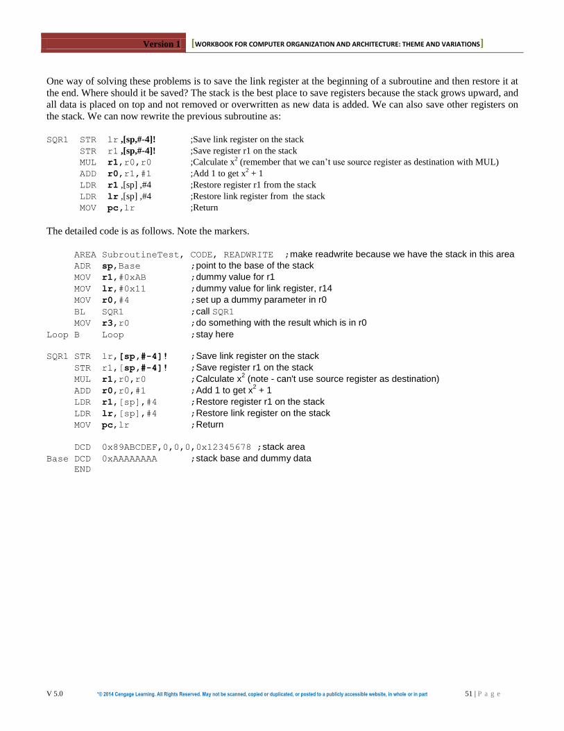
Version 1 [WORKBOOK FOR COMPUTER ORGANIZATION AND ARCHITECTURE: THEME AND VARIATIONS]
V 5.0 “© 2014 Cengage Learning. All Rights Reserved. May not be scanned, copied or duplicated, or posted to a publicly accessible website, in whole or in part 51 | P a g e
One way of solving these problems is to save the link register at the beginning of a subroutine and then restore it at
the end. Where should it be saved? The stack is the best place to save registers because the stack grows upward, and
all data is placed on top and not removed or overwritten as new data is added. We can also save other registers on
the stack. We can now rewrite the previous subroutine as:
SQR1 STR lr ,[sp,#-4]! ;Save link register on the stack
STR r1 ,[sp,#-4]! ;Save register r1 on the stack
MUL r1,r0,r0 ;Calculate x2 (remember that we can’t use source register as destination with MUL)
ADD r0,r1,#1 ;Add 1 to get x2 + 1
LDR r1 ,[sp] ,#4 ;Restore register r1 from the stack
LDR lr ,[sp] ,#4 ;Restore link register from the stack
MOV pc,lr ;Return
The detailed code is as follows. Note the markers.
AREA SubroutineTest, CODE, READWRITE ;make readwrite because we have the stack in this area
ADR sp,Base ;point to the base of the stack
MOV r1,#0xAB ;dummy value for r1
MOV lr,#0x11 ;dummy value for link register, r14
MOV r0,#4 ;set up a dummy parameter in r0
BL SQR1 ;call SQR1
MOV r3,r0 ;do something with the result which is in r0
Loop B Loop ;stay here
SQR1 STR lr,[sp,#-4]! ;Save link register on the stack
STR r1,[sp,#-4]! ;Save register r1 on the stack
MUL r1,r0,r0 ;Calculate x2 (note - can't use source register as destination)
ADD r0,r0,#1 ;Add 1 to get x2 + 1
LDR r1,[sp],#4 ;Restore register r1 on the stack
LDR lr,[sp],#4 ;Restore link register on the stack
MOV pc,lr ;Return
DCD 0x89ABCDEF,0,0,0,0x12345678 ;stack area
Base DCD 0xAAAAAAAA ;stack base and dummy data END

Version 1 [WORKBOOK FOR COMPUTER ORGANIZATION AND ARCHITECTURE: THEME AND VARIATIONS]
V 5.0 “© 2014 Cengage Learning. All Rights Reserved. May not be scanned, copied or duplicated, or posted to a publicly accessible website, in whole or in part 52 | P a g e
The next snapshot shows the situation at the point the subroutine SQR1 is called.

Version 1 [WORKBOOK FOR COMPUTER ORGANIZATION AND ARCHITECTURE: THEME AND VARIATIONS]
V 5.0 “© 2014 Cengage Learning. All Rights Reserved. May not be scanned, copied or duplicated, or posted to a publicly accessible website, in whole or in part 53 | P a g e
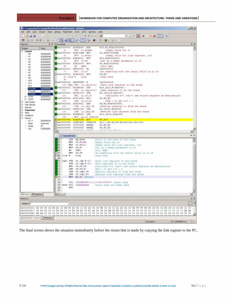
Version 1 [WORKBOOK FOR COMPUTER ORGANIZATION AND ARCHITECTURE: THEME AND VARIATIONS]
V 5.0 “© 2014 Cengage Learning. All Rights Reserved. May not be scanned, copied or duplicated, or posted to a publicly accessible website, in whole or in part 54 | P a g e
The final screen shows the situation immediately before the return that is made by copying the link register to the PC.

Version 1 [WORKBOOK FOR COMPUTER ORGANIZATION AND ARCHITECTURE: THEME AND VARIATIONS]
V 5.0 “© 2014 Cengage Learning. All Rights Reserved. May not be scanned, copied or duplicated, or posted to a publicly accessible website, in whole or in part 55 | P a g e

Version 1 [WORKBOOK FOR COMPUTER ORGANIZATION AND ARCHITECTURE: THEME AND VARIATIONS]
V 5.0 “© 2014 Cengage Learning. All Rights Reserved. May not be scanned, copied or duplicated, or posted to a publicly accessible website, in whole or in part 56 | P a g e
MULTIPLE SUBROUTINE CALLS
We next extend the example by demonstrating a multiple call. Here, we’ve used a typical CISC instruction BSR ABC to
implement the call. A branch to subroutine instruction automatically saves the return address on the stack (unlike the ARM that
saves it in the link register). Because subroutine return addresses are stacked, you can call subroutines from within a subroutine
(nesting). In the following figure, the main body of the code calls subroutine ABC. At the end of the subroutine, a return
instruction makes a return to the point immediately following the call. In this example, the subroutine is called from two
different places and yet a return is made to the correct point in each case.
In order to achieve this objective with the ARM processor, we can use the ARM’s block move instructions that copy multiple
registers to and from the stack.
USING BLOCK MOVE INSTRUCTIONS
In practice, programmers don’t use the simple code we’ve written above to save registers on the stack and to retrieve them.
Traditionally, RISC processors provide simple, regular instructions that take one cycle (in principle) to execute. The ARM
processor family is different because it has a set of instructions that perform multiple actions. These instructions are called
block move operations and are able to copy the contents of several registers to or from memory.
When you first encounter ARM’s block move instruction you are likely to be overwhelmed by their apparent complexity. In
fact, they are not complex; it’s just that there are several options to choose from. So, to keep things simple, we will just discuss
one option here. These two block move instructions we are going to use are:
STMFD ;Push a group of registers on the stack
LDMFD ;Pull a group of registers off the stack
Couldn’t be simpler. The STMFD mnemonic stands for store multiple registers full descending. The expression “full
descending” tells you two things. The term full means that the stack points at the top item on the stack. The term descending
tells you that the stack grows towards lower addresses as items are pushed. This is exactly the same type of stack we’ve already
described. When we wish to store data on the system stack, we have to use r13 which we can write as sp. We also have to write
sp! or r13! to tell the assembler that we want to use automatic indexing. Finally, we have to create a register list by enclosing
the registers to be moved between braces; that is, {r0,r1,r7} specifies registers r0, r1 and r7, We can use a dash to denote a
sequence of registers; for example {r0-r5,r8,r11} indicates the register list r0, r1, r2, r3, r4, r5, r8, and r11.
To push r0 and r1 on the stack, we write STMFD sp!,{r0,r1}. Similarly, to pull r1 and r2 off the stack, we write
LDMFD sp!,{r0,r1}
Suppose we use a different register list for the store and retrieve multiple register operations. What would happen if we execute
STMFD sp!,{r0,r1} then LDMFD sp!,{r5,r7}? Well, we push r0 and r1 and then we pull their values off the stack
and transfer them to registers r5 and r7, In other words, we’ve copied one group of registers into another group.

Version 1 [WORKBOOK FOR COMPUTER ORGANIZATION AND ARCHITECTURE: THEME AND VARIATIONS]
V 5.0 “© 2014 Cengage Learning. All Rights Reserved. May not be scanned, copied or duplicated, or posted to a publicly accessible website, in whole or in part 57 | P a g e
Let’s demonstrate these block move instructions in action.
AREA BlockMove,CODE,READWRITE ;make readwrite because we have the stack in this area
ADR sp,Base ;point to the base of the stack
MOV r0,#0xAB ;dummy value for r0
MOV r1,#0xCD ;dummy value for r1
MOV lr,#0xDE ;dummy value for link register, r14
BL SQR1 ;call Test
Loop B Loop ;stay here
Test STMFD sp!,{r0,r1,lr} ;save r0, r1, lr on the stack
MOV r0,#0x11 ;let’s do something pointless
MOV r1,#0x22 ;let’s do something pointless
MOV r14,#0x22 ;let’s change the link register
ADD r3,r0,r1 ;ladd r0 and r1 and put the result in r3
LDMFD sp!,{r0,r1,pc} ;pull r0, r1, lr off the stack
DCD 0x89ABCDEF,0,0,0,0x12345678 ;stack area
Base DCD 0xAAAAAAAA ;stack base and dummy data END
This code is built on the previous example and uses the same basic format and stack structure. We use markers in memory like
0xAAAAAAAA and register values like 0xAB so that we can see the data in memory when we come to debug the code. We’re
going to run this example and examine the state of the registers and memory at three points.
The next snapshot shows the situation immediately after the program has been loaded.
First data stored in
memory after the code.
Marker for the
base of the stack.

Version 1 [WORKBOOK FOR COMPUTER ORGANIZATION AND ARCHITECTURE: THEME AND VARIATIONS]
V 5.0 “© 2014 Cengage Learning. All Rights Reserved. May not be scanned, copied or duplicated, or posted to a publicly accessible website, in whole or in part 58 | P a g e
The next snapshot shows the state immediately before the branch with link instruction.
The next snapshot shows the state after we have called the subroutine and executed the first instruction.
r0 and r1 have been
set up.
Here’s the initial
dummy value of the link register.
Note that the stack
pointer is pointing at
location 0x44, the base
of the stack.
Here’s the data written on the stack. Starting at the highest address, the
link register (0x14), then r1 (0xCD),
and finally r0 (0xAB).
The stack pointer is now 0x38 because three 32-bit words
have been pushed on the stack
and 0x38 = 0x44 - 3 × 4.
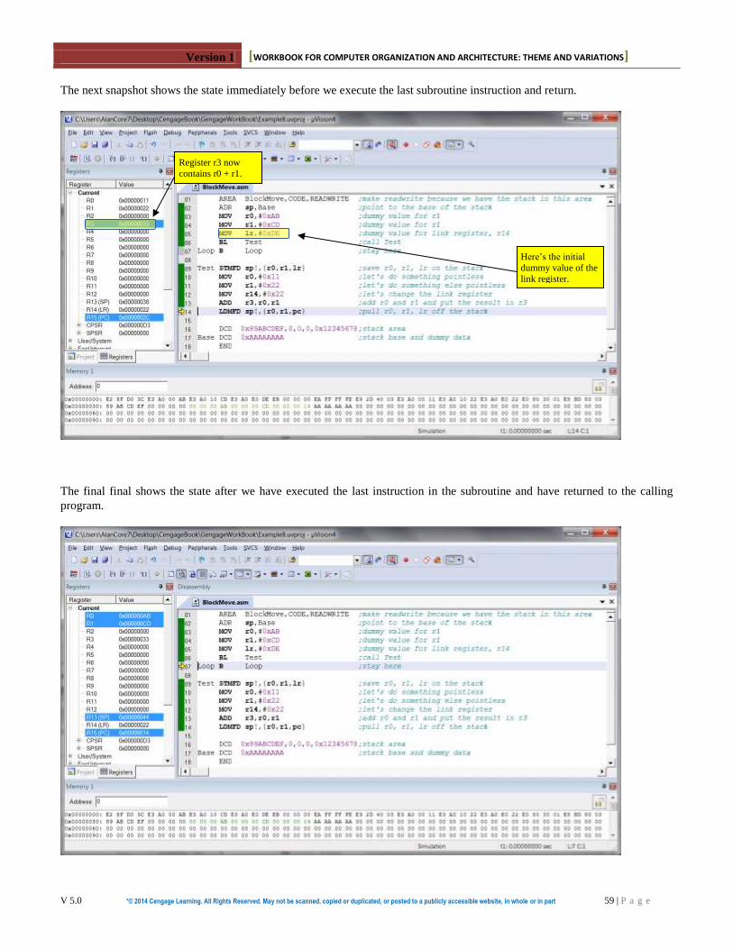
Version 1 [WORKBOOK FOR COMPUTER ORGANIZATION AND ARCHITECTURE: THEME AND VARIATIONS]
V 5.0 “© 2014 Cengage Learning. All Rights Reserved. May not be scanned, copied or duplicated, or posted to a publicly accessible website, in whole or in part 59 | P a g e
The next snapshot shows the state immediately before we execute the last subroutine instruction and return.
The final final shows the state after we have executed the last instruction in the subroutine and have returned to the calling
program.
Here’s the initial
dummy value of the
link register.
Register r3 now
contains r0 + r1.

Version 1 [WORKBOOK FOR COMPUTER ORGANIZATION AND ARCHITECTURE: THEME AND VARIATIONS]
V 5.0 “© 2014 Cengage Learning. All Rights Reserved. May not be scanned, copied or duplicated, or posted to a publicly accessible website, in whole or in part 60 | P a g e
PASSING A PARAMETER TO A SUBROUTINE
When you call a subroutine, you often have to pass parameters to the subroutine. In a high-level language you might call
subroutine XYZ with parameters P and Q by XYZ(P,Q). In a low-level language, you can push the parameters on the stack
immediately before calling the subroutine. Of course, you don’t have to pass parameters via the stack; for example, if there are
a very few, you can transfer them via registers.
Consider the following example where we have a very simple subroutine that adds two numbers P and Q and returns their
result S = P + Q. Using pseudocode, we can write the following sequence of actions that describes the passing of the two
parameters and the receiving of the result.
Push P
Push Q
Call ADD
Pull S
Adjust the stack
We push the two parameters on the stack and call the subroutine. The subroutine reads the two parameters off the top of the
stack, and replaces one by the result. Note that we have to adjust the stack to take account of the fact that we have pushed two
parameters but pulled only one. The stack must always be balanced with equal numbers of push and pull operations.
The next diagram shows the effect of pushing a parameter on the stack before calling a subroutine. State (a) demonstrates the
situation immediately before the subroutine is called. State (b) shows the situation in which both parameters have been pushed.
State (c) shows the situation in which a subroutine has been called and the return address is saved on the stack (typical of CISC
processors).
The next figure demonstrates the behavior of the stack during the subroutine execution.
Stack pointerTop of stack
SP
Memory
Stack pointer
SP
Memory
Stack pointer
SPMemory
(a) Initial stack (b) Stack after pushing P and Q © Stack after pushing the return address
0
-4
-12
0
-4
Return address
Parameter Q
Parameter P
-8 Parameter Q
Parameter P
-8 4
8
Stack pointerTop of stack
SP
Memory
Stack pointer
SP
Memory
Stack pointer
SPMemory
(a) Stack after the subroutinereads Q and P and stores thesum.
(b) Stack after returning fromsubroutine
(c) Stack after pulling the result
0
-4
-12
0
-4
Return address
Parameter P
-8Result S=P+Q
Parameter P
-8 4
8
Result S=P+Q
4 Stack pointer
SP
Memory
0
Parameter P
(d) Stack after adjusting the stack pointer
Version 1 [WORKBOOK FOR COMPUTER ORGANIZATION AND ARCHITECTURE: THEME AND VARIATIONS]
V 5.0 “© 2014 Cengage Learning. All Rights Reserved. May not be scanned, copied or duplicated, or posted to a publicly accessible website, in whole or in part 61 | P a g e
As you can see, the stack grows as parameters are pushed and the subroutine called. Then the stack declines as a return made
and the two items on the stack removed. Now, let’s look at this process in detail using an ARM processor.
USING THE STACK - AN ARM EXAMPLE
The following code sets up an environment and carries out the actions we have described.
AREA ParamTest,CODE,READWRITE ;make readwrite because of the stack ADR sp,Base ;point to the base of the stack
MOV r0,#0xAB ;dummy value for P in r0
MOV r1,#0xCD ;dummy value for Q in r1
STR r0,[sp,#-4]! ;push P
STR r1,[sp,#-4]! ;push Q
BL ADDR ;call the adder LDR r2,[sp],#4 ;pull S off the stack
ADD sp,sp,#4 ;adjust the stack pointer
Loop B Loop ;park here
ADDR STR lr,[sp,#-4]! ;push the link register on the stack
LDR r5,[sp,#8] ;get P (buried under the return address and Q)
LDR r6,[sp,#4] ;get q (buried under the return address)
ADD r5,r5,r6 ;do the addition
STR r5,[sp,#4] ;save result on the stack under return address (overwrite Q)
LDR pc,[sp],#4 ;pull return address off the stack
DCD 0,0,0,0,0 ;stack area
Base DCD 0xAAAAAAAA ;stack base and dummy data as marker END
The following snapshot demonstrates the situation when the program has been loaded.
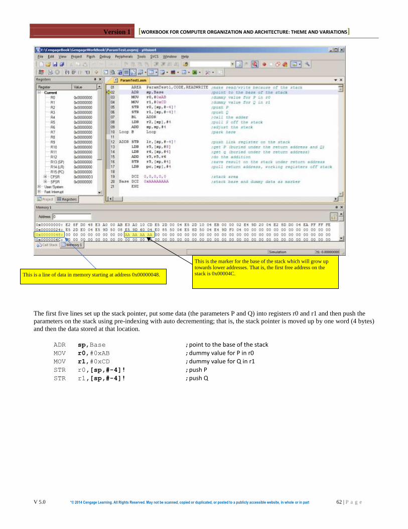
Version 1 [WORKBOOK FOR COMPUTER ORGANIZATION AND ARCHITECTURE: THEME AND VARIATIONS]
V 5.0 “© 2014 Cengage Learning. All Rights Reserved. May not be scanned, copied or duplicated, or posted to a publicly accessible website, in whole or in part 62 | P a g e
The first five lines set up the stack pointer, put some data (the parameters P and Q) into registers r0 and r1 and then push the
parameters on the stack using pre-indexing with auto decrementing; that is, the stack pointer is moved up by one word (4 bytes)
and then the data stored at that location.
ADR sp,Base ;point to the base of the stack
MOV r0,#0xAB ;dummy value for P in r0
MOV r1,#0xCD ;dummy value for Q in r1
STR r0,[sp,#-4]! ;push P
STR r1,[sp,#-4]! ;push Q
This is the marker for the base of the stack which will grow up
towards lower addresses. That is, the first free address on the stack is 0x00004C.
This is a line of data in memory starting at address 0x00000048.

Version 1 [WORKBOOK FOR COMPUTER ORGANIZATION AND ARCHITECTURE: THEME AND VARIATIONS]
V 5.0 “© 2014 Cengage Learning. All Rights Reserved. May not be scanned, copied or duplicated, or posted to a publicly accessible website, in whole or in part 63 | P a g e
The following snapshot demonstrates the situation before calling the subroutine (i.e., we are about to execute the branch with
link instruction).
These are the two
parameters pushed
on the stack

Version 1 [WORKBOOK FOR COMPUTER ORGANIZATION AND ARCHITECTURE: THEME AND VARIATIONS]
V 5.0 “© 2014 Cengage Learning. All Rights Reserved. May not be scanned, copied or duplicated, or posted to a publicly accessible website, in whole or in part 64 | P a g e
The snapshot of the system below shows situation in the subroutine after reading the two parameters and pushing the return
address. We have called a subroutine and loaded r14, the link register, with the return address, and then executed the following
code:
ADDR STR lr,[sp,#-4]! ;push the link register on the stack
LDR r5,[sp,#8] ;get P (buried under the return address and Q)
LDR r6,[sp,#4] ;get Q (buried under the return address)
This code first pushes the link register on the stack and then reads the two parameters off the stack. You will see that registers
r5 and r6 contain the same parameters are r0 and r1, and that the contents of the link register are now the topmost element on
the stack.
The link register,
r14, saved on the stack

Version 1 [WORKBOOK FOR COMPUTER ORGANIZATION AND ARCHITECTURE: THEME AND VARIATIONS]
V 5.0 “© 2014 Cengage Learning. All Rights Reserved. May not be scanned, copied or duplicated, or posted to a publicly accessible website, in whole or in part 65 | P a g e
The next snapshot shows the situation immediately before the return from subroutine. We have just executed
ADD r5,r5,r6 ;do the addition
STR r5,[sp,#4] ;save result on the stack under return address
These instructions perform the addition of the parameters in registers r5 and r6 and then store the result at [sp] + 4 which is one
word below the top of the stack; that is, the location of parameter Q. The following memory map shows that Q (in memory)
has changed from 0x000000CD to 0x00000178.
Parameter Q has
been overwritten by the result.

Version 1 [WORKBOOK FOR COMPUTER ORGANIZATION AND ARCHITECTURE: THEME AND VARIATIONS]
V 5.0 “© 2014 Cengage Learning. All Rights Reserved. May not be scanned, copied or duplicated, or posted to a publicly accessible website, in whole or in part 66 | P a g e
The final snapshot shows the situation at the end of the program when we have executed the following code.
LDR pc,[sp],#4 ;pull return address off the stack (last line of subroutine)
LDR r2,[sp],#4 ;pull S off the stack (first operation after the subroutine)
ADD sp,sp,#4 ;adjust the stack pointer
Loop B Loop ;park here
Note that this code is rewritten in execution order rather than program order; that is, the first line is the last operation in the
subroutine and the second line is the first instruction at the return point.
A return is made by pulling the link register off the stack and putting it in the program counter. In the calling routine, the top of
the stack is pulled (i.e., the result) and put in r2. Finally, the stack pointer is incremented by 4 to restore it to its original value.
We have pulled the
result off the stack and put it in r2.

Version 1 [WORKBOOK FOR COMPUTER ORGANIZATION AND ARCHITECTURE: THEME AND VARIATIONS]
V 5.0 “© 2014 Cengage Learning. All Rights Reserved. May not be scanned, copied or duplicated, or posted to a publicly accessible website, in whole or in part 67 | P a g e
IMPROVING THE CODE
Few programmers would write the code we used in the previous example. A more reasonable approach is:
AREA ParamTest1,CODE,READWRITE ;make readwrite because we locate the stack in this area ADR sp,Base ;point to the base of the stack
MOV r0,#0xAB ;dummy value for P in r0
MOV r1,#0xCD ;dummy value for Q in r1
STMFD sp!,{r0,r1} ;push P and Q
BL ADDR ;call the addition subroutine LDMFD sp!,{r0,r2} ;pull S and P off the stack
Loop B Loop ;park here
ADDR STMFD sp!,{r5,r6,lr} ;push the link register and working registers
LDR r5,[sp,#16] ;get P (buried under the return address and Q)
LDR r6,[sp,#12] ;get Q (buried under the return address)
ADD r5,r5,r6 ;do the addition
STR r5,[sp,#16] ;save result on the stack under the return address
LDMFD sp!,{r5,r6,pc} ;pull return address and working registers
DCD 0xFFFFFFFF,0,0,0,0,0 ;stack area
Base DCD 0xAAAAAAAA ;stack base and dummy data END
We need to look at some of the features of this program in greater detail.
STMFD sp!,{r0,r1} ;push P and Q
BL ADDR ;call the adder
LDMFD sp!,{r0,r2} ;pull S and P off the stack
Loop B Loop ;park here
ADDR STMFD sp!,{r5,r6,lr} ;push the link register and working
LDR r5,[sp,#16] ;get P (buried under the return address and Q)
LDR r6,[sp,#12] ;get q (buried under the return address)
ADD r5,r5,r6 ;do the addition
STR r5,[sp,#16] ;save result on the stack under return address
LDMFD sp!,{r5,r6,pc} ;pull return address and working registers
Note the locations of the two parameters. We have pushed a return
address, r5 and r6 (3 x 4 bytes = 12),
so that the two items are 12 and 16
bytes below the top of the stack.
Here we use the store multiple registers
instruction to push two parameters on the
stack.
We now store the result on the stack,
overwriting one of the original
parameters.
This is the return. We use load multiple
registers to restore the original r5 and r6 and
we pull the return address which we directly
load into the program counter, r15.
We use the load multiple registers
instruction to pull the result off the stack
and also balance the stack; that is, push 2
pull 2.
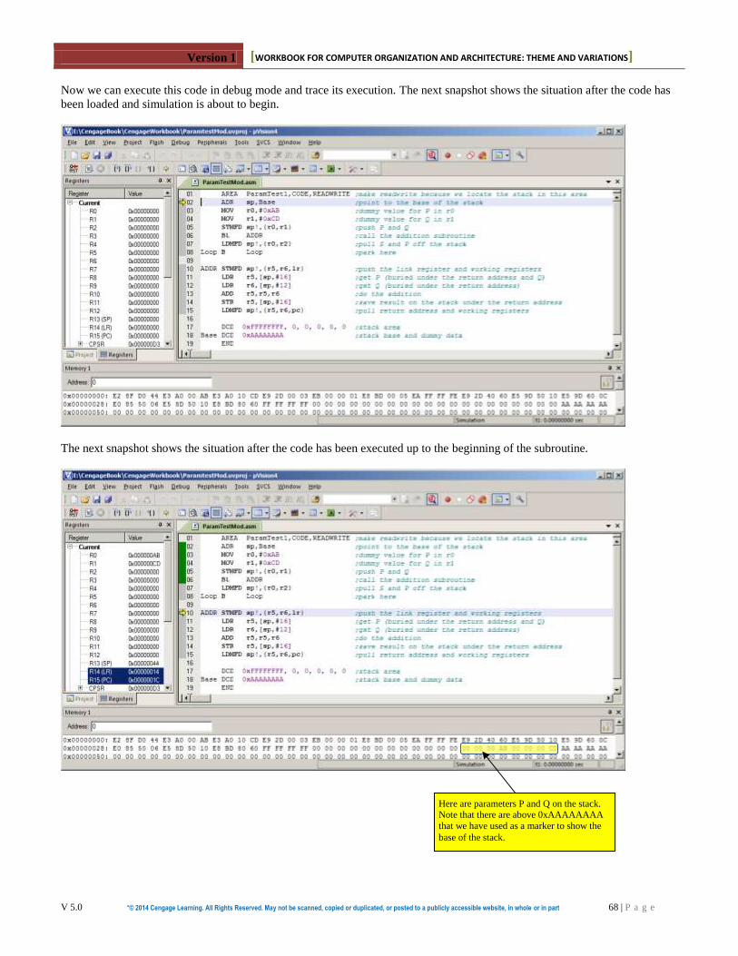
Version 1 [WORKBOOK FOR COMPUTER ORGANIZATION AND ARCHITECTURE: THEME AND VARIATIONS]
V 5.0 “© 2014 Cengage Learning. All Rights Reserved. May not be scanned, copied or duplicated, or posted to a publicly accessible website, in whole or in part 68 | P a g e
Now we can execute this code in debug mode and trace its execution. The next snapshot shows the situation after the code has
been loaded and simulation is about to begin.
The next snapshot shows the situation after the code has been executed up to the beginning of the subroutine.
Here are parameters P and Q on the stack. Note that there are above 0xAAAAAAAA
that we have used as a marker to show the
base of the stack.
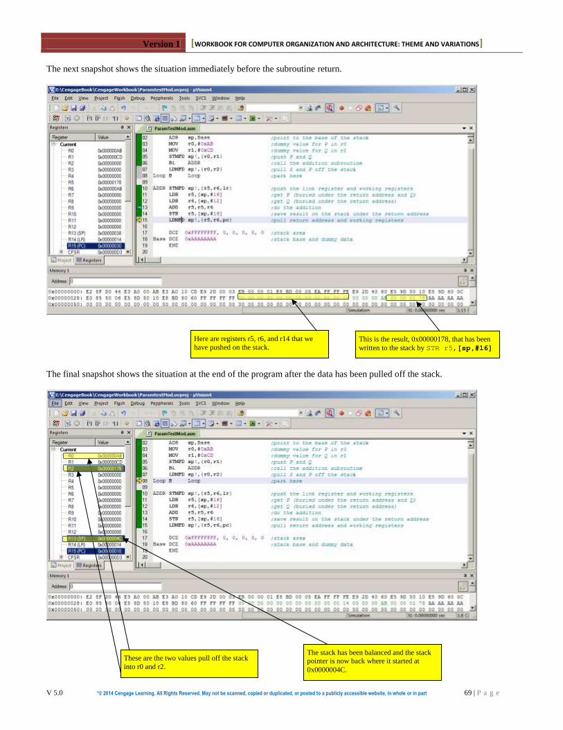
Version 1 [WORKBOOK FOR COMPUTER ORGANIZATION AND ARCHITECTURE: THEME AND VARIATIONS]
V 5.0 “© 2014 Cengage Learning. All Rights Reserved. May not be scanned, copied or duplicated, or posted to a publicly accessible website, in whole or in part 69 | P a g e
The next snapshot shows the situation immediately before the subroutine return.
The final snapshot shows the situation at the end of the program after the data has been pulled off the stack.
Here are registers r5, r6, and r14 that we
have pushed on the stack. This is the result, 0x00000178, that has been
written to the stack by STR r5,[sp,#16]
These are the two values pull off the stack
into r0 and r2.
The stack has been balanced and the stack pointer is now back where it started at
0x0000004C.

Version 1 [WORKBOOK FOR COMPUTER ORGANIZATION AND ARCHITECTURE: THEME AND VARIATIONS]
V 5.0 “© 2014 Cengage Learning. All Rights Reserved. May not be scanned, copied or duplicated, or posted to a publicly accessible website, in whole or in part 70 | P a g e
PASSING A PARAMETER BY ITS ADDRESS
Some languages let you pass parameters by reference rather than by value; that is, you send the address of the parameter to a
subroutine. The 68K processor has a push effective address instruction, PEA that pushes a 32-bit address on the stack. ARM
programmers have to use conventional memory store instructions.
When you retrieve a parameter passed by reference (address), you have to pull the address off the stack (or read it from the
stack) and then access the parameter by means of address register indirect addressing. Consider the following fragment of code
that pushes an address (initially in register r0), call a subroutine, and then retrieves the actual parameter (i.e., its value) in the
subroutine..
STR r0,[sp,#-4]! ;Push the address of parameter P on the stack (address is in r0)
BL ABC ;Call subroutine ABC and save the link register .
ABC STR lr,[sp,#-4]! ;Save the return address on the stack LDR r1,[sp,#4] ;Read the address of parameter P under the return address
LDR r2,[r1] ;Get the value of parameter P .
LDMFD sp!,{pc} ;Return by loading the PC with the return address from the stack
Retrieving a parameter by reference is a two-step operation. The first part is to get the parameter’s address, and the second part
is to get the value pointed at by that address. In this case we first load the address of P using LDR r1,[sp,#4]to get the
address of P in r1 and then use LDR r2,[r1]to get the value of P in r2. We have put these two lines in blue to highlight their
importance.
Let’s use this code in an actual program. Below, we use subroutine ABC to perform P + 1. The effect of this program should be
to add 1 to P’s initial value 0x12345678 to give 0x12345679 in the memory location defined as P. Since there are 11
instructions before this location, the address of P is 0x0000002C (i.e., 11 x 4 expressed in hexadecimal).
AREA PassByRef,CODE,READWRITE ; Make readwrite because we locate the stack in this area ADR sp,Base ; Point to the base of the stack
ADR r0,P ; Load r0 with the address of parameter P
STR r0,[sp,#-4]! ; Push the address of parameter P on the stack (address is in r0)
BL ABC ; Call subroutine ABC and save the link register
Moi B Moi ; Infinite loop to end the program
ABC STR lr,[sp,#-4]! ; Save the return address on the stack
LDR r1,[sp,#4] ; Read the address of parameter P under the return address
LDR r2,[r1] ; Get the value of parameter P
ADD r2,r2,#1 ; Add 1 to P
STR r2,[r1] ; Save the parameter in the calling environment
LDMFD sp!,{pc} ; Return by loading the PC with the return address from the stack
P DCD 0x12345678 ; Location of parameter P and its value
DCD 0xFFFFFFFF,0,0,0,0,0 ; Stack area
Base DCD 0xAAAAAAAA ; Stack base and dummy data END
The first instruction, ADR sp,Base, loads the stack pointer with the initial base of the stack, and the second instruction, ADR
r0,P, loads r0 with the address of P. It is important to stress here that we are loading the address of P (0x0000002C) and not
it’s value (0x12345678).
The following snapshot demonstrates the situation immediately after the program has been loaded. We’ve highlighted the data
area and the stack.

Version 1 [WORKBOOK FOR COMPUTER ORGANIZATION AND ARCHITECTURE: THEME AND VARIATIONS]
V 5.0 “© 2014 Cengage Learning. All Rights Reserved. May not be scanned, copied or duplicated, or posted to a publicly accessible website, in whole or in part 71 | P a g e
The next snapshot shows the state of the system up to the start of the subroutine. You can see that r0 contains the address of
parameter P (i.e., 0x0000002C). The stack pointer has been moved up from its initial value of 0x00000040 to 0x00000044.
Stack base marker End of code and data
marker The space we’ve
left for the stack 0x000004C
This is the value of P
(0x12345678) at memory
location 0x0000002C.
The address of P on the stack
The stack pointer has changed
from 0x00000048 to 0x00000044

Version 1 [WORKBOOK FOR COMPUTER ORGANIZATION AND ARCHITECTURE: THEME AND VARIATIONS]
V 5.0 “© 2014 Cengage Learning. All Rights Reserved. May not be scanned, copied or duplicated, or posted to a publicly accessible website, in whole or in part 72 | P a g e
The next snapshot traced execution to the point at which the address of P has been read off the stack into r1, but the value of P
has not yet been loaded into r2.
The final snapshot shows the sitiation at the end of the program. The value of P in memory has been updated.
The link register
saved on the stack
Register r1 now holds the address
of P
The value of P in memory.
It’s been updated.
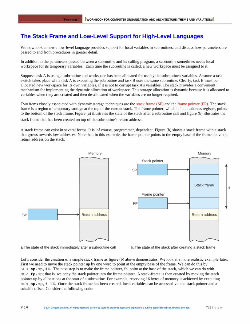
Version 1 [WORKBOOK FOR COMPUTER ORGANIZATION AND ARCHITECTURE: THEME AND VARIATIONS]
V 5.0 “© 2014 Cengage Learning. All Rights Reserved. May not be scanned, copied or duplicated, or posted to a publicly accessible website, in whole or in part 73 | P a g e
The Stack Frame and Low-Level Support for High-Level Languages We now look at how a low-level language provides support for local variables in subroutines, and discuss how parameters are
passed to and from procedures in greater detail.
In addition to the parameters passed between a subroutine and its calling program, a subroutine sometimes needs local
workspace for its temporary variables. Each time the subroutine is called, a new workspace must be assigned to it.
Suppose task A is using a subroutine and workspace has been allocated for use by the subroutine's variables. Assume a task
switch takes place while task A is executing the subroutine and task B uses the same subroutine. Clearly, task B must be
allocated new workspace for its own variables, if it is not to corrupt task A's variables. The stack provides a convenient
mechanism for implementing the dynamic allocation of workspace. This storage allocation is dynamic because it is allocated to
variables when they are created and then de-allocated when the variables are no longer required.
Two items closely associated with dynamic storage techniques are the stack frame (SF) and the frame pointer (FP). The stack
frame is a region of temporary storage at the top of the current stack. The frame pointer, which is in an address register, points
to the bottom of the stack frame. Figure (a) illustrates the state of the stack after a subroutine call and figure (b) illustrates the
stack frame that has been created on top of the subroutine’s return address.
A stack frame can exist in several forms. It is, of course, programmer, dependent. Figure (b) shows a stack frame with a stack
that grows towards low addresses. Note that, in this example, the frame pointer points to the empty base of the frame above the
return address on the stack.
Let’s consider the creation of a simple stack frame as figure (b) above demonstrates. We look at a more realistic example later.
First we need to move the stack pointer up by one word to point at the empty base of the frame. We can do this by
SUB sp,sp,#4. The next step is to make the frame pointer, fp, point at the base of the stack, which we can do with
MOV fp,sp; that is, we copy the stack pointer into the frame pointer. A stack-frame is then created by moving the stack
pointer up by d locations at the start of a subroutine. For example, reserving 16 bytes of memory is achieved by executing
sub sp,sp,#-16. Once the stack frame has been created, local variables can be accessed via the stack pointer and a
suitable offset. Consider the following code:
SP
FP
a.The state of the stack immediately after a subroutine call b. The state of the stack after creating a stack frame
Frame pointer
Return address Return address
SP
Stack pointer
Stack framed
Memory Memory

Version 1 [WORKBOOK FOR COMPUTER ORGANIZATION AND ARCHITECTURE: THEME AND VARIATIONS]
V 5.0 “© 2014 Cengage Learning. All Rights Reserved. May not be scanned, copied or duplicated, or posted to a publicly accessible website, in whole or in part 74 | P a g e
AnySub SUB sp,sp,#4 ;Move the stack pointer up one word past the return address on the stack
MOV fp,sp ;Set up the frame pointer to point to the top of the stack
SUB sp,sp,#16 ;Move the stack pointer to the top of the stack frame (we’ll allocate 16 bytes) .
. ;The subroutine proper (i.e., the code goes here)
.
ADD sp,sp,#20 ;Collapse the stack frame (i.e., 16 + 4)
MOV pc,lr ;and return from subroutine
Before a return from subroutine is made, the stack frame must be collapsed by an ADD sp,sp,#20 instruction. This simply
moves the stack pointer down. In practice, this code would not be used, because it doesn’t preserve the old frame pointer; that
is, the frame pointer is destroyed by this code.
A better way of implementing a stack frame is to save the old frame pointer on the stack before creating the frame itself; that is,
AnySub SUB sp,sp,#4 ; Move the stack pointer up to create space for the old frame pointer
STR fp,[sp] ; Save the old (existing) frame pointer on the stack
MOV fp,sp ; Set up the frame pointer to point to the base of the stack
SUB sp,sp,#16 ; move the stack pointer to the top of the stack frame .
. ; The subroutine proper .
MOV sp,fp ; Restore the stack pointer and collapse the frame
LDR fp,[sp],#4 ; Restore the old (existing) frame pointer on the stack
ADD sp,sp,#4 ; Move the stack pointer down to point to the return address
MOV pc,lr ; and return from subroutine
In practice the code would be more compact with the ARM’s facilities (e.g., auto incrementing and decrementing addressing
modes) being better used. Consider the following example. In this case consider the following example where a subroutine is
called using a BL instruction (branch with link). In this case the return address is not saved on the stack.
BL ABCD ;Call subroutine ABCD
;
;
ABCD STR fp,[sp,#-4]! ;Save the old frame pointer on the stack (pre-indexing)
MOV fp,sp ;Set up the frame pointer to point to the base of the stack
SUB sp,sp,#16 ;Move the stack pointer to the top of the stack frame .
. ;The subroutine proper .
MOV sp,fp ;Restore the stack pointer and collapse the frame
LDR fp,[sp],#4 ;Restore the old frame pointer on the stack and post-increment the stack
MOV pc,lr ;Return
The following snapshot of the simulator demonstrates this fragment of code in the simulator using some dummy data to keep
track of register values.

Version 1 [WORKBOOK FOR COMPUTER ORGANIZATION AND ARCHITECTURE: THEME AND VARIATIONS]
V 5.0 “© 2014 Cengage Learning. All Rights Reserved. May not be scanned, copied or duplicated, or posted to a publicly accessible website, in whole or in part 75 | P a g e
Up to now, we’ve demonstrated simple examples of stack frames. The next step is to provide a more realistic (albeit simple)
example. This example will demonstrate various aspects of machine-level programming; for example, the use of registers
(global and local), the use of temporary storage (stack frames), and parameter passing.
PASSING PARAMETERS TO AND FROM A STACK FRAME
We are going to use a subroutine that is called by pushing the return address on the stack. We pass two parameters to the stack;
one by value and one by reference. Let’s assume that the stack performs B = A2 + B, where A is passed by reference and B by
value.
In this example, we use two registers in the subroutine, r1 and r2, that are saved on the stack at the start of the subroutine by a
store multiple registers and then retrieved at the end of the subroutine by a load multiple registers. One register, r0, is a global
scratchpad and does not have to be preserved by the subroutine. Finally, we create a stack frame for one variable in the
subroutine.
The code for this example is given below. We have created initial dummy values for registers so you can see them when they
are saved in memory and used 0xFFFFFFFF as the stack base in order to make the stack visible in the memory map.
AREA FrameParams, CODE, READWRITE
ADR sp,Stack ;set up the stack pointer
LDR fp,=0xAAAAAAAA ;dummy value for fp
LDR r1,=0x11111111 ;dummy value for r1
LDR r2,=0x22222222 ;dummy value for r2
ADR r3,A ;r3 is a pointer to A
LDR r4,[r3] ;get parameter A
STR r4,[sp,#-4]! ;push the value of A on the stack
ADR r5,B ;get the address of B
STR r5,[sp,#-4]! ;push the address of B on the stack
BL SumSq ;call the subroutine
LSR r0,[r5] ;if it worked, r0 should contain 7
Again B Again ;parking loop

Version 1 [WORKBOOK FOR COMPUTER ORGANIZATION AND ARCHITECTURE: THEME AND VARIATIONS]
V 5.0 “© 2014 Cengage Learning. All Rights Reserved. May not be scanned, copied or duplicated, or posted to a publicly accessible website, in whole or in part 76 | P a g e
SumSq STMDB sp!,{r1,r2,lr} ;save registers on the stack
STR fp,[sp,#-4]! ;Save the old frame pointer on the stack (pre-indexing)
MOV fp,sp ;Set up the frame pointer to point to the base of the stack
SUB sp,sp,#4 ;Move the stack pointer to the top of the one-word stack frame
LDR r1,[fp,#20] ;Get the value of A off the stack in r1
MUL r2,r1,r1 ;Square A
STR r2,[fp,#-4] ;Store the value of A squared in the stack frame
LDR r2,[fp,#16] ;Get the address of B off the stack in r2 (reuse r2)
LDR r1,[r2] ;Get the value of B in r1 (reuse r1)
LDR r0,[fp,#-4] ;Get the value of A squared in r0
ADD r1,r1,r0 ;Add B to A squared
STR r1,[r2] ;Return the result to the calling environment
MOV sp,fp ;Restore the stack pointer and collapse the frame
LDR fp,[sp],#4 ;Restore the old frame pointer on the stack and post-increment the stack
LDMIA sp!,{r1,r2,pc} ;Restore registers and return
A DCD 2 ;dummy value for A
B DCD 3 ;dummy value for B
SPACE 16 ;reserve 16 bytes for the stack
Stack DCD 0xFFFFFFFF ;dummy data for the base of the stack END
The next simulator snapshot shows the simulator window when the program is first loaded.
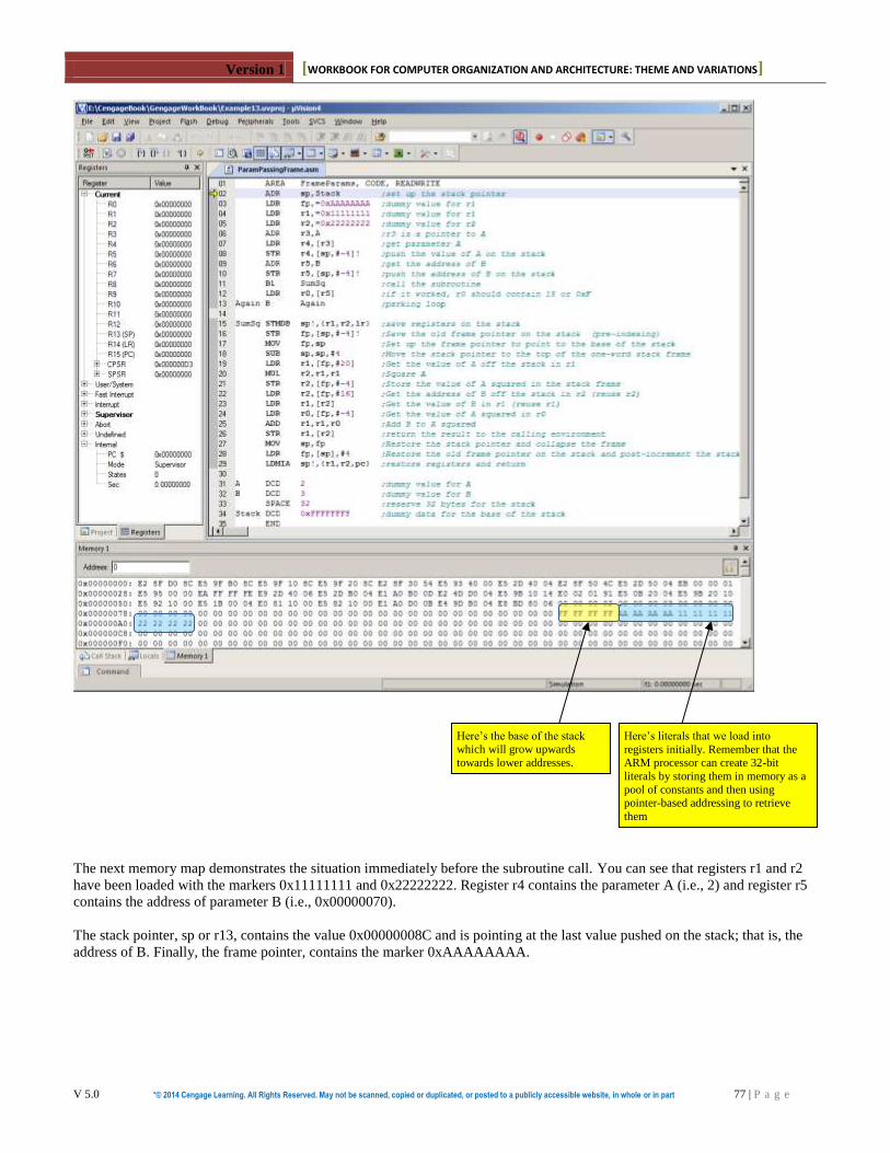
Version 1 [WORKBOOK FOR COMPUTER ORGANIZATION AND ARCHITECTURE: THEME AND VARIATIONS]
V 5.0 “© 2014 Cengage Learning. All Rights Reserved. May not be scanned, copied or duplicated, or posted to a publicly accessible website, in whole or in part 77 | P a g e
The next memory map demonstrates the situation immediately before the subroutine call. You can see that registers r1 and r2
have been loaded with the markers 0x11111111 and 0x22222222. Register r4 contains the parameter A (i.e., 2) and register r5
contains the address of parameter B (i.e., 0x00000070).
The stack pointer, sp or r13, contains the value 0x00000008C and is pointing at the last value pushed on the stack; that is, the
address of B. Finally, the frame pointer, contains the marker 0xAAAAAAAA.
Here’s literals that we load into
registers initially. Remember that the
ARM processor can create 32-bit
literals by storing them in memory as a
pool of constants and then using pointer-based addressing to retrieve
them
Here’s the base of the stack which will grow upwards
towards lower addresses.

Version 1 [WORKBOOK FOR COMPUTER ORGANIZATION AND ARCHITECTURE: THEME AND VARIATIONS]
V 5.0 “© 2014 Cengage Learning. All Rights Reserved. May not be scanned, copied or duplicated, or posted to a publicly accessible website, in whole or in part 78 | P a g e
The next memory map shows the situation in the subroutine after saving r1, r2, and the link register on the stack.
The stack pointer contains 0x0000008C
and is pointing here
at the address of B on
the stack.
This is parameter B with the value 3 at memory
location 0x00000070.
This is parameter A with the value 3 at
memory location
0x0000006C.
Here is the value of
parameter A (i.e., 2) on the stack at
address 0x00000090.

Version 1 [WORKBOOK FOR COMPUTER ORGANIZATION AND ARCHITECTURE: THEME AND VARIATIONS]
V 5.0 “© 2014 Cengage Learning. All Rights Reserved. May not be scanned, copied or duplicated, or posted to a publicly accessible website, in whole or in part 79 | P a g e
The following figure demonstrates the structure of the stack in this example. Note that addresses on the left are given with
respect to the frame pointer. This helps to relate the stack to the offsets in the above code.
Direction ofgrowth as itemsare added
Stack pointer Top of stack
MemoryLow memory
The stack base
Parameters pushedon the stack
r1 = 0x111111111
r2 = 0x22222222
lr (r13) = 0x00000028
Saved on entry tothe subroutine
0xAAAAAAAA
The stack frame
Frame pointer pointer
fp + 4
fp + 12
fp + 8
fp - 4
fp + 16
fp + 20 0x2 Value of A
0x70 Address of B
0xFFFFFFFF
fp
The stack pointer contains 0x00000080 and is pointing at
the sequence r1, r2, r13 (the link register containing the
return address 0x00000028),
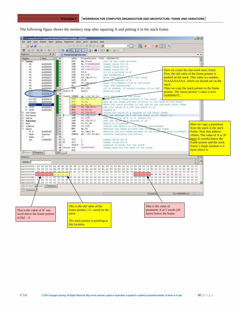
Version 1 [WORKBOOK FOR COMPUTER ORGANIZATION AND ARCHITECTURE: THEME AND VARIATIONS]
V 5.0 “© 2014 Cengage Learning. All Rights Reserved. May not be scanned, copied or duplicated, or posted to a publicly accessible website, in whole or in part 80 | P a g e
The following figure shows the memory map after squaring A and putting it in the stack frame.
This is the old value of the frame pointer, r11, saved on the
stack.
The stack pointer is pointing at
this location.
Here we create the one-word stack frame. First, the old value of the frame pointer is
pushed on the stack. This value is a marker,
0xAAAAAAAA, which we should see on the stack.
Then we copy the stack pointer to the frame
pointer. The frame pointer’s value is now
0x0000007C.
Here we copy a parameter
from the stack to the stack frame. Note that address
offsets. The value of A is 20
bytes (5 words) below the frame pointer and the stack
frame’s single location is 4
bytes above it.
This is the value of A2 one word above the frame pointer
at [fp] – 4.
This is the value of parameter A at 5 words (20
bytes) below the frame pointer.

Version 1 [WORKBOOK FOR COMPUTER ORGANIZATION AND ARCHITECTURE: THEME AND VARIATIONS]
V 5.0 “© 2014 Cengage Learning. All Rights Reserved. May not be scanned, copied or duplicated, or posted to a publicly accessible website, in whole or in part 81 | P a g e
The next memory map shows the situation after storing the result in the calling environment and before cleaning up the stack
frame.
Here’s the rest of the computation. At the start of this
code, the value of A2 is in the
stack frame at [fp] – 4.
We first retrieve the address of
parameter B off the stack at 4 words (16 bytes) below the
frame pointer. The address is
loaded into r2. The red lines show the contents of 2 and the
location pointed at. This
location contains 7, the final value of B, because the
following codes changes the
original value from 3 to 3 + 22.
The next operation,
LDR r0,[fp,#-4] loads the
value of A2 that we’ve saved in the stack frame. We then add
this to the value of B and save
the sum in B in the calling environment using the pointer in
r2. This is the end of the
computation.

Version 1 [WORKBOOK FOR COMPUTER ORGANIZATION AND ARCHITECTURE: THEME AND VARIATIONS]
V 5.0 “© 2014 Cengage Learning. All Rights Reserved. May not be scanned, copied or duplicated, or posted to a publicly accessible website, in whole or in part 82 | P a g e
In the final snapshot of memory we show the memory map at the end of the program. A return has been made to the calling
program and we have completed the program and are in a parking loop. All the registers have been reset to their original values
except r13, the stack pointer, the program counter, and r0 which was a global scratchpad register.
The point of this example was to demonstrate the stack frame and passing parameters both be reference and value.
This is both a good example and a bad example. It is good in the sense that it is relatively simple. It is bad in the sense that no
one would write this code because a stack frame is not necessary because there are enough registers for the local storage.
However, this example does illustrate how much overhead is associated with accessing data in memory.

Version 1 [WORKBOOK FOR COMPUTER ORGANIZATION AND ARCHITECTURE: THEME AND VARIATIONS]
V 5.0 “© 2014 Cengage Learning. All Rights Reserved. May not be scanned, copied or duplicated, or posted to a publicly accessible website, in whole or in part 83 | P a g e
APPENDIX
ARM Mnemonics
This appendix provides brief details of the part of the ARM’s instruction set. We haven’t included instructions that operate on
the coprocessor.
ADC Add with carry Rd Rn + Op2 + Carry
ADD Add Rd Rn + Op2
AND AND Rd Rn AND Op2
B Branch R15 address
BIC Bit Clear Rd Rn AND NOT Op2
BL Branch with Link R14 R15, R15 address
BX Branch and Exchange R15 Rn, T bit Rn[0]
CMN Compare Negative CPSR flags Rn + Op2
CMP Compare CPSR flags Rn - Op2
EOR Exclusive OR Rd Rn Op2 LDM Load multiple registers
LDR Load register from memory Rd [address]
MLA Multiply Accumulate Rd := (Rm Rs) + Rn
MOV Move register or constant Rd Op2
MRS Move PSR status/flags to Register Rn PSR
MSR Move register to PSR status/flags PSR Rm
MUL Multiply Rd Rm Rs
MVN Move negative register Rd 0xFFFFFFFF EOR Op
ORR OR Rd Rn OR Op2
RSB Reverse Subtract Rd Op2 - Rn
RSC Reverse Subtract with Carry Rd Op2 - Rn - 1 + Carry
SBC Subtract with Carry Rd Rn - Op2 - 1 + Carry STM Store Multiple
STR Store register to memory [address] Rd
SUB Subtract Rd Rn - Op2 SWI Software Interrupt OS call
SWP Swap register with memory Rd [Rn], [Rn] Rm
TEQ Test bitwise equality CPSR flags Rn EOR Op2
TST Test bits CPSR flags Rn AND Op2