Embed Size (px)
Citation preview

Computer Organziation andArchitecture Lab
Department of Computer Engineering
Khwaja Fareed University of Engineering andInformation Technology
Rahim Yar Khan, Pakistan
Contents
1 Lab 1 11.1 Objective . . . . . . . . . . . . . . . . . . . . . . . . . . . . . . . . . . . . . . . . . 11.2 Introduction . . . . . . . . . . . . . . . . . . . . . . . . . . . . . . . . . . . . . . . 11.3 Architecture . . . . . . . . . . . . . . . . . . . . . . . . . . . . . . . . . . . . . . . 11.4 Program Counter . . . . . . . . . . . . . . . . . . . . . . . . . . . . . . . . . . . . 11.5 Input and MAR . . . . . . . . . . . . . . . . . . . . . . . . . . . . . . . . . . . . . 21.6 RAM . . . . . . . . . . . . . . . . . . . . . . . . . . . . . . . . . . . . . . . . . . . 31.7 Instruction Register . . . . . . . . . . . . . . . . . . . . . . . . . . . . . . . . . . . 3
2 Lab 2 42.1 Objective . . . . . . . . . . . . . . . . . . . . . . . . . . . . . . . . . . . . . . . . . 42.2 Introduction . . . . . . . . . . . . . . . . . . . . . . . . . . . . . . . . . . . . . . . 42.3 Controller-Sequencer . . . . . . . . . . . . . . . . . . . . . . . . . . . . . . . . . . 42.4 Accumulator . . . . . . . . . . . . . . . . . . . . . . . . . . . . . . . . . . . . . . . 52.5 The Adder-Subtractor . . . . . . . . . . . . . . . . . . . . . . . . . . . . . . . . . 52.6 B Register . . . . . . . . . . . . . . . . . . . . . . . . . . . . . . . . . . . . . . . . 52.7 Output Register . . . . . . . . . . . . . . . . . . . . . . . . . . . . . . . . . . . . . 62.8 Binary Display . . . . . . . . . . . . . . . . . . . . . . . . . . . . . . . . . . . . . . 62.9 Instruction Set . . . . . . . . . . . . . . . . . . . . . . . . . . . . . . . . . . . . . . 6
3 Lab 3 73.1 Objective . . . . . . . . . . . . . . . . . . . . . . . . . . . . . . . . . . . . . . . . . 73.2 Components Required . . . . . . . . . . . . . . . . . . . . . . . . . . . . . . . . . 73.3 Description . . . . . . . . . . . . . . . . . . . . . . . . . . . . . . . . . . . . . . . . 73.4 Procedure . . . . . . . . . . . . . . . . . . . . . . . . . . . . . . . . . . . . . . . . 83.5 How to check the output . . . . . . . . . . . . . . . . . . . . . . . . . . . . . . . . 8
4 Lab 4 94.1 Objective . . . . . . . . . . . . . . . . . . . . . . . . . . . . . . . . . . . . . . . . . 94.2 Components Required . . . . . . . . . . . . . . . . . . . . . . . . . . . . . . . . . 94.3 What is Program Counter . . . . . . . . . . . . . . . . . . . . . . . . . . . . . . . 94.4 MAR (Memory Address Register) . . . . . . . . . . . . . . . . . . . . . . . . . . 94.5 2-to-1 Nibble Multiplexer (Input unit) . . . . . . . . . . . . . . . . . . . . . . . . 94.6 2-to-1 Nibble Multiplexer (Input unit) . . . . . . . . . . . . . . . . . . . . . . . . 104.7 Procedure . . . . . . . . . . . . . . . . . . . . . . . . . . . . . . . . . . . . . . . . 104.8 How to check the output . . . . . . . . . . . . . . . . . . . . . . . . . . . . . . . . 11
5 Lab 5 125.1 Objective . . . . . . . . . . . . . . . . . . . . . . . . . . . . . . . . . . . . . . . . . 125.2 Components Required . . . . . . . . . . . . . . . . . . . . . . . . . . . . . . . . . 125.3 16x8 RAM . . . . . . . . . . . . . . . . . . . . . . . . . . . . . . . . . . . . . . . . 125.4 Instruction Register . . . . . . . . . . . . . . . . . . . . . . . . . . . . . . . . . . 12
ii

Contents iii
5.5 Procedure . . . . . . . . . . . . . . . . . . . . . . . . . . . . . . . . . . . . . . . . 125.6 How to check the output . . . . . . . . . . . . . . . . . . . . . . . . . . . . . . . . 13
6 Lab 6 146.1 Objective . . . . . . . . . . . . . . . . . . . . . . . . . . . . . . . . . . . . . . . . . 146.2 Components Required . . . . . . . . . . . . . . . . . . . . . . . . . . . . . . . . . 146.3 SAP-1 Instruction Set . . . . . . . . . . . . . . . . . . . . . . . . . . . . . . . . . . 14
6.3.1 Mnemonics . . . . . . . . . . . . . . . . . . . . . . . . . . . . . . . . . . . 146.3.2 Memory-Reference Instructions . . . . . . . . . . . . . . . . . . . . . . . 156.3.3 LDA . . . . . . . . . . . . . . . . . . . . . . . . . . . . . . . . . . . . . . . 156.3.4 ADD . . . . . . . . . . . . . . . . . . . . . . . . . . . . . . . . . . . . . . . 156.3.5 SUB . . . . . . . . . . . . . . . . . . . . . . . . . . . . . . . . . . . . . . . 156.3.6 OUT . . . . . . . . . . . . . . . . . . . . . . . . . . . . . . . . . . . . . . . 156.3.7 HLT . . . . . . . . . . . . . . . . . . . . . . . . . . . . . . . . . . . . . . . . 156.3.8 Programming SAP-1 . . . . . . . . . . . . . . . . . . . . . . . . . . . . . . 156.3.9 Instruction Decoder . . . . . . . . . . . . . . . . . . . . . . . . . . . . . . 166.3.10 R . . . . . . . . . . . . . . . . . . . . . . . . . . . . . . . . . . . . . . . . . 166.3.11 Address State . . . . . . . . . . . . . . . . . . . . . . . . . . . . . . . . . . 166.3.12 Increment State . . . . . . . . . . . . . . . . . . . . . . . . . . . . . . . . . 166.3.13 Fetch cycle . . . . . . . . . . . . . . . . . . . . . . . . . . . . . . . . . . . . 176.3.14 Execution cycle . . . . . . . . . . . . . . . . . . . . . . . . . . . . . . . . . 17
6.4 Procedure . . . . . . . . . . . . . . . . . . . . . . . . . . . . . . . . . . . . . . . . 17
7 Lab 7 197.1 Objective . . . . . . . . . . . . . . . . . . . . . . . . . . . . . . . . . . . . . . . . . 197.2 Components Required . . . . . . . . . . . . . . . . . . . . . . . . . . . . . . . . . 197.3 Accumulator . . . . . . . . . . . . . . . . . . . . . . . . . . . . . . . . . . . . . . . 197.4 Adder/Subtractor . . . . . . . . . . . . . . . . . . . . . . . . . . . . . . . . . . . 197.5 Procedure . . . . . . . . . . . . . . . . . . . . . . . . . . . . . . . . . . . . . . . . 207.6 What shall be the Lab’s Outcome? . . . . . . . . . . . . . . . . . . . . . . . . . . 20
8 Lab 8 218.1 Objective . . . . . . . . . . . . . . . . . . . . . . . . . . . . . . . . . . . . . . . . . 218.2 Components Required . . . . . . . . . . . . . . . . . . . . . . . . . . . . . . . . . 218.3 B Register . . . . . . . . . . . . . . . . . . . . . . . . . . . . . . . . . . . . . . . . 218.4 Output Register . . . . . . . . . . . . . . . . . . . . . . . . . . . . . . . . . . . . . 218.5 Binary Display . . . . . . . . . . . . . . . . . . . . . . . . . . . . . . . . . . . . . . 218.6 Procedure . . . . . . . . . . . . . . . . . . . . . . . . . . . . . . . . . . . . . . . . 218.7 What shall be the lab’s outcome? . . . . . . . . . . . . . . . . . . . . . . . . . . . 22
9 Lab 9 239.1 Objective . . . . . . . . . . . . . . . . . . . . . . . . . . . . . . . . . . . . . . . . . 239.2 Description . . . . . . . . . . . . . . . . . . . . . . . . . . . . . . . . . . . . . . . . 239.3 Step1: Create a Directory for your Project . . . . . . . . . . . . . . . . . . . . . . 239.4 Step2: Start ModelSim and Create a Project . . . . . . . . . . . . . . . . . . . . . 249.5 Step3: Add Your Verilog to the Project . . . . . . . . . . . . . . . . . . . . . . . . 249.6 Step4. Compile your Verilog files . . . . . . . . . . . . . . . . . . . . . . . . . . . 249.7 Step5. Start the simulation. . . . . . . . . . . . . . . . . . . . . . . . . . . . . . . 259.8 Step6: Add Signals to the Wave Window . . . . . . . . . . . . . . . . . . . . . . 25

iv Contents
10 Lab 10 2610.1 Objective . . . . . . . . . . . . . . . . . . . . . . . . . . . . . . . . . . . . . . . . . 2610.2 D flip-flop . . . . . . . . . . . . . . . . . . . . . . . . . . . . . . . . . . . . . . . . 26
10.2.1 Verilog Code for D flip flop . . . . . . . . . . . . . . . . . . . . . . . . . . 2610.2.2 Verilog Testbench code to simulate and verify D Flip-Flop . . . . . . . . 27
10.3 Multiplexer . . . . . . . . . . . . . . . . . . . . . . . . . . . . . . . . . . . . . . . 2810.3.1 Verilog code for Multiplexer . . . . . . . . . . . . . . . . . . . . . . . . . 2810.3.2 Verilog Testbench code to simulate Multiplexer . . . . . . . . . . . . . . 28
11 Lab 11 3011.1 Objective . . . . . . . . . . . . . . . . . . . . . . . . . . . . . . . . . . . . . . . . . 3011.2 Description . . . . . . . . . . . . . . . . . . . . . . . . . . . . . . . . . . . . . . . . 30
11.2.1 Verilog code for Multiplexer . . . . . . . . . . . . . . . . . . . . . . . . . 3011.2.2 Verilog code for Adder . . . . . . . . . . . . . . . . . . . . . . . . . . . . 3111.2.3 Verilog code for Instruction Memory . . . . . . . . . . . . . . . . . . . . 31
11.3 Tasks for Students . . . . . . . . . . . . . . . . . . . . . . . . . . . . . . . . . . . . 32
12 Lab 11 3312.1 Objective . . . . . . . . . . . . . . . . . . . . . . . . . . . . . . . . . . . . . . . . . 3312.2 Description . . . . . . . . . . . . . . . . . . . . . . . . . . . . . . . . . . . . . . . . 33
12.2.1 Verilog Code for Data Memory . . . . . . . . . . . . . . . . . . . . . . . . 3312.2.2 Verilog code for Left Shifter . . . . . . . . . . . . . . . . . . . . . . . . . . 3512.2.3 Verilog code for Sign Extention . . . . . . . . . . . . . . . . . . . . . . . . 35
12.3 Tasks for Students . . . . . . . . . . . . . . . . . . . . . . . . . . . . . . . . . . . . 36
13 Lab 13 3713.1 Objective . . . . . . . . . . . . . . . . . . . . . . . . . . . . . . . . . . . . . . . . . 3713.2 Description . . . . . . . . . . . . . . . . . . . . . . . . . . . . . . . . . . . . . . . . 37
13.2.1 Verilog Code for Register File . . . . . . . . . . . . . . . . . . . . . . . . . 3713.2.2 Verilog code for ALU . . . . . . . . . . . . . . . . . . . . . . . . . . . . . 39
13.3 Tasks for Students . . . . . . . . . . . . . . . . . . . . . . . . . . . . . . . . . . . . 41
14 Lab 13 4214.1 Objective . . . . . . . . . . . . . . . . . . . . . . . . . . . . . . . . . . . . . . . . . 4214.2 Description . . . . . . . . . . . . . . . . . . . . . . . . . . . . . . . . . . . . . . . . 42
14.2.1 Verilog Code for Complete Processor . . . . . . . . . . . . . . . . . . . . 4214.3 Tasks for Students . . . . . . . . . . . . . . . . . . . . . . . . . . . . . . . . . . . . 49

Chapter 1
Lab 1
1.1 Objective
Introduction of Simple As Possible computer.
1.2 Introduction
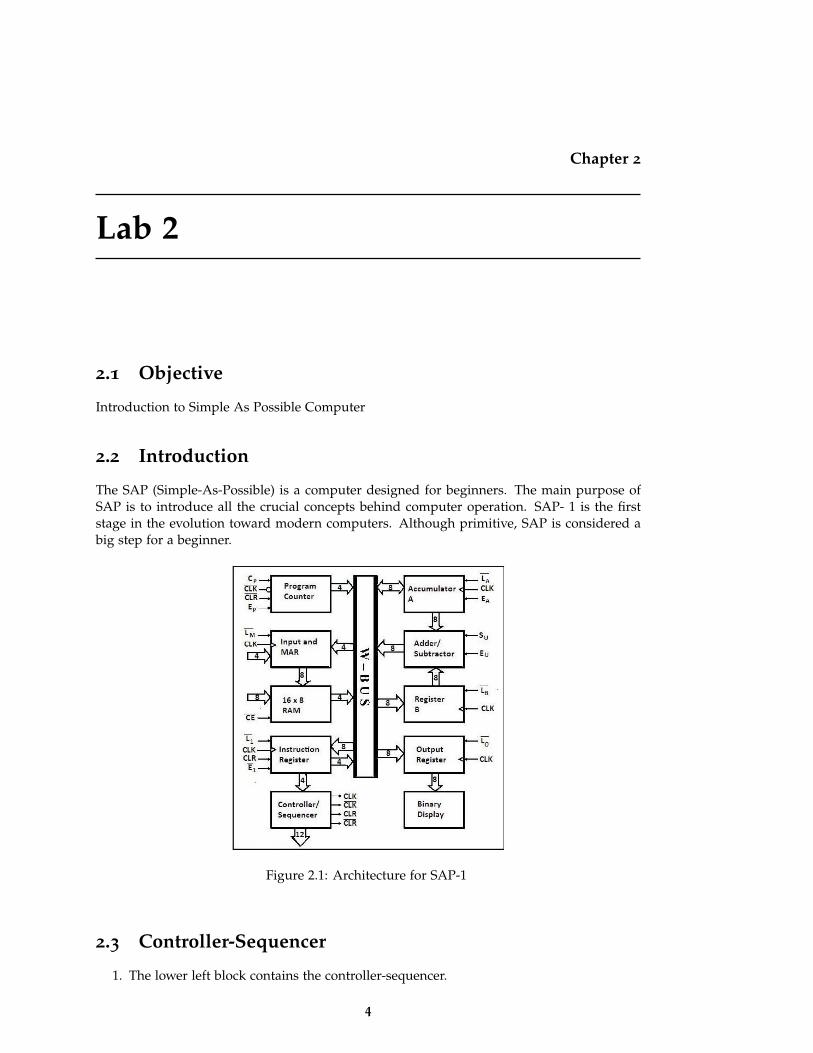
The SAP (Simple-As-Possible) is a computer designed for beginners. The main purpose ofSAP is to introduce all the crucial concepts behind computer operation. SAP- 1 is the firststage in the evolution toward modern computers. Although primitive, SAP is considered abig step for a beginner.
1.3 Architecture
Figure 1-1 shows the architecture of SAP-1, a bus-organized computer. All register outputsto the 8 bit W-bus are three states; this allows orderly transfer of data. All other registeroutputs are two state; these outputs continuously drive the boxes they are connected to. Thelayout of Fig. 1-1 emphasizes the registers used in SAP- 1. For this reason, no attempt hasbeen made to keep all control circuits in one block called the control unit, all input-outputcircuits in another block called the I/O unit, etc.
1.4 Program Counter
1. The program is stored at the beginning of the memory with the first instruction atbinary address 0000, the second instruction at address 0001, the third at address 0010,and so on.
2. The program counter, which is part of the control unit, counts from 0000 to 1111.
3. Its job is to send to the memory the address of the next instruction to be fetched andexecuted. It does this as follows.
(a) The program counter is reset to 0000 before each computer run.
(b) When the computer run begins, the program counter sends address 0000 to thememory.
(c) The program counter is then incremented to get 0001.
1

2 Lab 1
Figure 1.1: Architecture for SAP-1
(d) After the first instruction is fetched and executed, the program counter sends ad-dress 0001 to the memory.
(e) Again the program counter is incremented.(f) After the second instruction is fetched and executed, the program counter sends
address 0010 to the memory.
4. In this way, the program counter is keeping track of the next instruction to be fetchedand executed.
5. The program counter is like someone pointing a finger at a list of instructions, sayingdo this first, do this second do this third, etc.
6. This is why the program counter is sometimes called a pointer; it points to an addressin memory where something important is being stored
1.5 Input and MAR
1. Below the program counter is the input and MAR block.
2. It includes the address and data switch registers.
3. These switch registers, which are part of the input unit, allow you to send 4 addressbits and 8 data bits to the RAM.
4. As you recall, instruction and data words are written into the RAM before a computerrun.
5. The memory address register (MAR) is part of the SAP-1 memory.
6. During a computer run, the address in the program counter is latched into the MAR.
7. A bit later, the MAR applies this 4-bit address to the RAM, where a read operation isperformed.
§1.6 RAM 3
1.6 RAM
1. The RAM is 16x8 static TTL RAM.
2. It can be programmed by means of address and data switch registers.
3. During a computer operation, the RAM receives a 4-bit address from MAR and a readoperation is performed.
4. In this way, an instruction or data word stored in RAM is placed on the W bus for usein some other part of the computer.
1.7 Instruction Register
1. The instruction register is part of the control unit.
2. To fetch an instruction from the memory the computer does a memory read operation.
3. This places the contents of the addressed memory location on the W bus.
4. At the same time, the instruction register is set up for loading on the next positive clockedge.
5. The contents of the instruction register are split into two nibbles.
6. The upper nibble is a two-state output that goes directly to the block labeled "Controller-sequencer".
Chapter 2
Lab 2
2.1 Objective
Introduction to Simple As Possible Computer
2.2 Introduction
The SAP (Simple-As-Possible) is a computer designed for beginners. The main purpose ofSAP is to introduce all the crucial concepts behind computer operation. SAP- 1 is the firststage in the evolution toward modern computers. Although primitive, SAP is considered abig step for a beginner.
Figure 2.1: Architecture for SAP-1
2.3 Controller-Sequencer
1. The lower left block contains the controller-sequencer.
4

§2.4 Accumulator 5
2. Before each computer run, CLR a signal is sent, to the program counter and a CLRsignal to the instruction register.
3. This resets the program counter to 0000 and wipes out the last instruction in instructionregister.
4. A clock signal CLK is sent to all buffer registers; this synchronizes the operation of thecomputer, ensuring that things happen when they are supposed to happen. In otherwords, all register transfers occur on the positive edge of a common CLK signal.
5. Notice that a CLK signal also goes to the program counter.
6. The 12 bits that come out of the controller-sequencer form a word controlling the restof the computer (like a supervisor telling others what to do.) The 12 wires carrying thecontrol word are called the control bus.
7. LM mean that the contents of the program counter are latched into the MAR on thenext positive clock edge.
8. As another example, a low CE and a low LA mean that the addressed RAM word willbe transferred to the accumulator on the next positive clock edge.
2.4 Accumulator
1. The accumulator (A) is a buffer register that stores intermediate answers during a com-puter run. In Fig. 2-1 the accumulator has two outputs.
2. The two-state output goes directly to the adder-Subtractor.
3. The three-state output goes to the W bus.
4. Therefore, the 8-bit accumulator word, continuously drives the adder-Subtractor thesame word appears on the W bus when EA is high.
2.5 The Adder-Subtractor
1. SAP-1 uses a 2’s-complement adder-Subtractor.
2. The adder-Subtractor is asynchronous (un-clocked); this means that its contents canchange as soon as the input words change.
3. When is high, these contents appear on the W bus.
2.6 B Register
1. The B register is another buffer register.
2. It is used in arithmetic operations. A low LBâAZ and positive clock edge load the wordon the W bus into the B register.
3. The two-state output of the B register drives the adder-Subtractor, supplying the num-ber to be added or subtracted from the contents of the accumulator.
6 Lab 2
2.7 Output Register
1. At the end of a computer run, the accumulator contains the answer to the problembeing solved.
2. At this point, we need to transfer the answer to the outside world.
3. This is where the output register is used. When EA is high and L0âAZ is low, the nextpositive clock edge loads the accumulator word into the output register.
4. The output register is often called an output port because processed data can leave thecomputer through this register.
5. In microcomputers the output ports are connected to interface circuits that drive pe-ripheral devices like printers, cathode-ray tubes, teletypewriters, and so forth. (Aninterface circuit prepares the data to drive each device.)
2.8 Binary Display
1. The binary display is a row of eight light-emitting diodes (LEDs).
2. Because each LED connects to one flip-flop of the output port, the binary display showsus the contents of the output port.
3. Therefore, after we’ve transferred an answer from the accumulator to the output port,we can see the answer in binary form
2.9 Instruction Set
1. A computer is a useless pile of hardware until someone programs it.
2. This means loading step-by-step instructions into the memory before the start of acomputer run.
3. The SAP-I instruction set consist on five instructions as given below:
(a) LDA
(b) ADD
(c) SUB
(d) OUT
(e) HLT
Chapter 3
Lab 3
3.1 Objective
To build up a circuit that generates Clear and the Clock signal, that is part of the ControlUnit of SAP-1 computer.
3.2 Components Required
• Quad two input NAND gate IC, 74LS 00
• Quad three input NAND gate IC, 74LS1 0
• Hex Inverter IC, 74LS04
• 555 Timer IC
• Dual J-K Flip Flop
• Two Push button switches Connecting wires
3.3 Description
The clock circuit as is shown in the figure 2.1 consists of mainly a 555 Timer and a J-K flipflop. 555 Timer produces a 2-kHz clock signal with a 75% duty cycle at its output, and a J-Kflip flop, that divides the signal down to 1-kHz and also produces a 50% duty cycle.
Clock Buffers, which are two inverters, are used to produce the final clock signal, one CLKand other inverted CLKsignal. These are used here so that the clock signal being generatedis able to drive low-power Schottky TTL loads.
Clear- Start Debouncer produces two outputs, CLR for the Instruction Register and theinverted CLR’ for the Program Counter and Ring Counter. S5 is a push button switch. Whendepressed, it goes to the clear position generating a high CLR and a low CLR’. When S5 isreleased, it returns to the START position, producing a low CLR and a high CLR’.
SAP-1 runs in either of the two modes, manual or automatic. In manual you press andrelease S6 to generate one clock pulse. When S6 is depressed, CLK is high; when releasedCLK is low. In other words, the single-step debouncer generates T states one at a time asyou press and release the button. This allows you to step through the different T states whiletroubleshooting or debugging.
Switch S7 is a single pole double throw SPDT switch that can remain in either the MAN-UAL or the AUTO position. When in Manual the single-step button is active. When in AUTO
7

8 Lab 3
Figure 3.1: Clock Circuit for SAP-1
mode, the computer runs automatically. Two of the NAND gates are used to debounce theMANUAL-AUTO switch.
3.4 Procedure
• Connect the circuit as shown in the circuit diagram.
• Check the signals with the oscilloscope and get your work verified by your Lab instruc-tor.
• You will be graded for this Lab on the output and functionality of your circuit.
• For connections refer to the Pin configurations of the ICs.
3.5 How to check the output
• Check output with the help of oscilloscopeat CLK port.
• Measure Clock Period.
• Measure frequencyand duty cycle.

Chapter 4
Lab 4
4.1 Objective
To make the circuit of program counter for sap-1 that generates a 4-bit address code ofmemory, Input MAR and 2 to 1 Multiplexer
4.2 Components Required
• Dual JK Flip Flop IC, 74LS107
• Quad three state switch IC, 74LS126
• 4 bit D-type Register, 74LS173
• Quad 2-to-1 Data Selector/ Multiplexer IC, 74LS157
• connecting wires
4.3 What is Program Counter
The program counter, which is a part of control unit, counts according to the available RAM-memory. Its job is to send memory the address of the next instruction to be fetched andexecuted. Program counter is also called pointer sometimes, as it works like pointing at alist of instructions stored at different addresses in the memory, saying do this first, do thissecond etc.
4.4 MAR (Memory Address Register)
Chip C4, is a 74LS173, 4 bit buffer register. It serves as the MAR. Notice that pins 1 and2 are grounded; this converts the three-state output to a two-state output. In other words,the output of the MAR is not connected to the W bus, and so there’s no need to use thethree-state output.
4.5 2-to-1 Nibble Multiplexer (Input unit)
Chip C5 is a 74LS157 2-to-1 nibble multiplexer. The left nibble (pins 14, 11, 5 & 2) come fromthe address switch register S1 (these are just 4 DIP switches of your trainer and will be used
9

10 Lab 4
to manually program your RAM). The right nibble (pins 13, 10, 6, 3) comes from the MAR.The RUN-PROG switch S2 selects the nibble to reach to the output of C5. When S2 is in thePROG position (i.e. when it is low), the nibble out of the address switch register is selected.On the other hand, when S2 is in the RUN position (i.e. when it is high), the output of theMAR is selected.
4.6 2-to-1 Nibble Multiplexer (Input unit)
Chip C5 is a 74LS157 2-to-1 nibble multiplexer. The left nibble (pins 14, 11, 5 & 2) come fromthe address switch register S1 (these are just 4 DIP switches of your trainer and will be usedto manually program your RAM). The right nibble (pins 13, 10, 6, 3) comes from the MAR.The RUN-PROG switch S2 selects the nibble to reach to the output of C5. When S2 is in thePROG position (i.e. when it is low), the nibble out of the address switch register is selected.On the other hand, when S2 is in the RUN position (i.e. when it is high), the output of theMAR is selected.
4.7 Procedure
Connect the circuit as shown in the diagram.
Figure 4.1: Program Counter and MAR
Strobe G’ Select A’/B A B Output Y
1 X X X 00 0 0 X 00 0 1 X 10 1 X 0 00 1 X 1 1

§4.8 How to check the output 11
4.8 How to check the output
• Connect CP, EP, CLR’ to logic level 1 and LM’ to logic level 0.
• Connect CLK’ and CLK to the output of push button of trainer board (A AND A’ ORB AND B’).
• Now the output of the 74LS157 will be A0,A1,A2 and A3.
• Run/prog switch is connected to logic 0, and the output of 74LS157 will be a 4 bitcounter that will count from 0 to 15 on each clock pulse when Run/prog switch isconnected to logic level 1.

Chapter 5
Lab 5
5.1 Objective
To make the circuit of 16x8 RAM & Instruction-Register.
5.2 Components Required
• 16x4 ,74189
• 4 bit D-type Register IC, 74LS173
• Connecting Wiress
5.3 16x8 RAM
The chips used here are 74189s. Each chip is a 16 X 4 static RAM . Together, they give us a16 X 8 read-write memory. S3 is a data switch register (8-bit), and S4 is a read- write switch(a push button switch). To program the memory, S2 is put in the PROG position, this takethe CE input low (pin 2). The address and data switches are than set to the correct addressand data words. A momentary push of the read -write switch takes WEâAZ low (pin3) andloads the memory. After the program and data are in memory, the RUN-PROG switch (S2)is put in the run position in preparation for the computer run.
5.4 Instruction Register
The chips used are 74LS173s. Each chip is a 4-bit three-state buffer register. The two chipsare the instruction-register. Grounding pins 1 and 2 of C8 convert the three state output to atwo-state output, I7, I6, I5 and I4 this nibble goes to the instruction decoder in the controllersequencer. Signal E1 controls the output of C9, the lower nibble in the instruction register.When E1 is low, this nibble is placed on word bus.
5.5 Procedure
Connect the circuit as shown in the diagram.
12

§5.6 How to check the output 13
Figure 5.1: 16x8 RAM
Figure 5.2: Instruction Register
5.6 How to check the output
As this lab is a continuation of previous one so by keeping the switch of Multiplexer onPROG mode address the RAM location through switches A0 to A3, and then write someinverted instruction by keeping the switches of RAM on Write & PROG mode.
Afterwards try to read the instruction by keeping the switch of Multiplexer on RUN modeand using the higher nibble for addressing the specific location, and keeping the switches ofRAM on READ & RUN mode.
Instruction register should be able to read instruction from RAM, when LI’ is active andby making the LE’ pin active the upper nibble (op code) should be ready for control matrixcircuit and lower nibble (memory address) should be ready to be fed to the MAR.

Chapter 6
Lab 6
6.1 Objective
To build up the circuit of the Control Unit of SAP-1 computer including the instructionDecoder, the Ring Counter and the Control Matrix this generates the Control Word for SAP-1.
6.2 Components Required
• Quad two input Nand gate IC, 74LS00
• Tri three input Nand gate lC, 74LS10
• Dual four input Nand gate IC, 74LS20
• Hex Inverter IC, 74LS04
• Dual J-K Flip Flop IC, 74LS107
• Connecting wires
6.3 SAP-1 Instruction Set
Sap-1 computer has five instructions set. This instruction set is a list of basic operations thecomputer can perform. The instructions are:
1. LDA
2. ADD
3. SUB
4. OUT
5. HLT
6.3.1 Mnemonics
LDA, ADD, SUB, OUT, HIT represent the abbreviated form of the Instruction set, calledMnemonics.
14

§6.3 SAP-1 Instruction Set 15
6.3.2 Memory-Reference Instructions
LDA, ADD and SUB are memory referenced instructions because they use the data stored inmemory. OUT and HLT are not memory referenced instructions since they do not use datastored in memory.
6.3.3 LDA
LDA stands for "Load the Accumulator" instruction. A complete LDA instruction includesthe hexadecimal address of the data to be loaded.LDA 8H for instance means load the Accu-mulator with the data 8H.
6.3.4 ADD
ADD is another SAP-1 instruction. A complete ADD instruction includes the address of theword to be added. For instance Add 9H means add the contents of memory location 9H tothe contents of the accumulator; the sum replaces the original contents of accumulator. Firstthe contents of 9H are loaded into B register, and instantly the adder-subtractor forms thesum of A and B.
6.3.5 SUB
A complete SUB instruction includes the address of the word to be subtracted. For exampleSUB CH means subtract the contents of memory location CH from the contents of the accu-mulator. First contents of CH are loaded into B register and then instantly adder-subtractorforms the difference of A and B.
6.3.6 OUT
The OUT instruction transfers the contents of accumulator to the Output port. After itsexecution the answer to the problem in the program can be seen on the LED display. OUT isnot memory referenced instruction; it does not need an address.
6.3.7 HLT
HLT stands for Halt. This instruction tells the computer to stop processing data. HLT marksthe end of a program similar to the way a period marks the end of a sentence. You must use aHLT instruction at the end of every SAP-1 program; otherwise you get computer trash. HLTis complete in itself; it does not require RAM word since this instruction does not involvememory.
6.3.8 Programming SAP-1
To load an instruction in memory we have to use some kind of code that the computer caninterpret. Following table shows this code. The number 0000 stands for LDA, 0001 for ADD,0010 for SUB, 1110 for OUT and 1111 for HLT. Since this code tells the computer whichoperation to perform, it is called the Op-code.
• LDA 000
• ADD 0

16 Lab 6
• SUB 0001
• OUT 001
• HLT 0
6.3.9 Instruction Decoder
A hex inverter produces complements of the opcode bits 17, 16, 15 and 14. Then the 4input NAND gates decode the five output signals LDA, ADD, SUB, OUT, HLT. HLT is theonly active low signal, while all others are active high. When the HLT instruction is in theInstruction Register, all bits 17, 16, 15 and 14 are 1111 and HLT is low. This signal returnsto the single step clock (you made in Lab #3). In either case that is AUTO or MANUAL theclock stops and the computer run ends.
6.3.10 R
ing CounterThe Ring counter sometimes called the State Counter consists of three flip flop chips,
74LS107. This counter is reset whenever the Clear-Start button S5 is pressed. The output ofthe last flip flop is inverted so that the Q output drives the J input of the first flip flop. Dueto this T1 output is initially high. The CLK signal drives an active low input; this means thatthe negative edge of the CLK signal initiates each T state. Output of Ring Counter is: T=T6T5T4T3T2T1 At the beginning of a computer run, the ring word is T=000001 Successiveclock pulses produce ring words: T=000010
• T=000100
• T=001000
• T=010000
• T=100000
Then the Ring Counter reset to 000001 and the cycle repeats. Each ring word represents oneT state. The initial state T1 starts with a negative clock edge and ends with next negativeclock edge. During this T state the T1 output of the ring counter is high. During the nextstate T2 is high; the following state T3 is high and so on. As you can see the ring counterproduces six T states. Each instruction is fetched and executed during these six T states.
6.3.11 Address State
The T1 state is called the address state because the address in the PC is transferred to theMAR during this state. During this state, EP and LM’ are active; all other control bits areinactive. This means that the controller sequencer is sending out a control word of:
CON 0 1 0 1 1 1 1 0 0 0 1 1
6.3.12 Increment State
During Increment State T2 only CP is active, causing the PC to increment to the next memorylocation.
CON 1 0 1 1 1 1 1 0 0 0 1 1

§6.4 Procedure 17
6.3.13 Fetch cycle
The address, increment and memory states are called the fetch cycle of SAP-1.
6.3.14 Execution cycle
1. The next three states T4, T5 and T6 are the three states of the execution cycle of SAP-1.The register transfer during this execution depends on a particular instruction beingexecuted. Each instruction has its own control routine.
2. The LDA, SUB, ADD and OUT signals from the instruction decoder drives the ControlMatrix.
3. At the same time, the Ring Counter signals, T1 to T6 also drive the matrix.
4. The matrix produces CON, a 12-bit microinstruction that, tells the rest of the computerwhat to do. State CON Active Bits
• T1 5E3H EP, L’P• T2 BE3H CP
• T3 263H C’E, L’I
5. The Control unit is the key to a computer’s automatic operation.
6. The Control unit generates the control words that fetch and execute each instruction.
7. While each instruction is fetched and executed, the computer passes through differentT states, or timing states, that is periods during which register contents change.
6.4 Procedure
1. Connect the circuit as shown in the circuit diagram.
2. Connect 17, 16, 15 and 14 to dip switches on your trainer and give the different op-codesfor different instructions.
3. For instance for HLT’ instruction, op-code is 1111, this means keeping all dip switchesin "Hi" position will generate an active low HLT’ signal, similarly you can check forother instructions.
4. Check the signals with the oscilloscope and get your work verified by your Lab instruc-tor.
5. You will be graded for this Lab on the output and functionality of your circuit.

18 Lab 6
Figure 6.1: Ring Counter

Chapter 7
Lab 7
7.1 Objective
To make the circuit of accumulator register and a 4-bit adder/subtractor.
7.2 Components Required
• 4 bit D-type Register IC, 74LS173
• 4 bit Bus Buffer (Quad three state switch) IC, 74LS126
• 4 bit Full Adder IC, 74LS83
• Connecting wires
7.3 Accumulator
The Accumulator is a buffer register that stores intermediate answers during a computer run.The accumulator has both a two state and a three state output. The two state output goesdirectly to the adder/subtractor and the three state output goes to the W bus via a buffer.Therefore, the 8 bit Accumulator word continuously drives the adder/subtractor; the sameword appears on the W bus when EA is high. Chips C10 and C11, 74LS173s, make up theaccumulator. Pins 1 and 2 are grounded on both chips to produce a two state output forthe adder/subtractor. Chips C12 and C13 are 74LS126s; these three-state switches place theaccumulator contents on the W bus when EA is high.
7.4 Adder/Subtractor
SAP-1 uses a 2’s complement adder/subtractor. When SU is low, the sum out of the addersubtracter is A = A + B. When SU is high, the difference appears A = A + B’ + 1 (Recallthat the 2’s complement is equivalent to a decimal sign change). The adder/subtractor isasynchronous (un-clocked); this means that its contents changes as soon as the input wordschange. When EU is high, these contents appear on the W bus Chips C14 and C15 are74LS86s. These ex-or gates are a controlled inverter. When SU is low, the contents of theB register are transmitted. When Su is high, the 1’s complement is transmitted and a 1 isadded to the LSB to form the 2’s complement. Chips C16 and C17 are 74LS83s. These 4-bitfull adders combine to produce an 8-bit sum or difference. Chips C18 and C19, which are74LS128s, convert the 8-bit answer into a three-state output for driving the W bus.
19

20 Lab 7
7.5 Procedure
Make the connections as shown in circuit diagram.
Figure 7.1: Accumulator and Adder/Subtractor
7.6 What shall be the Lab’s Outcome?
The input to the Accumulator should be through switches, which will be one 8-Bit data num-ber to add/sub. There should be a static 8- bit number (let’s say binary one) as the other inputto the adder/subtractor. The output of the adder/subtractor should be connected to LEDs.By proper input to the SU pin. The LEDs should be showing the results of adder/subtractor.
Chapter 8
Lab 8
8.1 Objective
To make and connect B-register and output-register through the Bus, And to read the contentsof output register through binary display.
8.2 Components Required
4 bit D type register IC, 74LS1 734 4 LEDs
8.3 B Register
The B register is a buffer register. It is used in arithmetic operations. A low LB and a positiveclock edge load the word on the W bus into the B register. The two state output of the Bregister drives the Adder/ Subtracter, supplying the number to be added or subtracted fromthe contents of the accumulator.
8.4 Output Register
At the end of the computer run the accumulator contains the answer to the problem beingsolved, at this point, we need to transfer the answer to the outside world, and this is wherethe output register is used. When EA is high and Lo is low, the next positive clock edge loadsthe accumulator word into the output register.
8.5 Binary Display
The binary display is a row of eight light-emitting LEDs because each LED is connected toone pin of the output register the binary display shows the contents of the output register.
8.6 Procedure
Connect the circuit as shown in the circuit diagram.
21

22 Lab 8
Figure 8.1: B-Register, Output Register, and Binary Display
8.7 What shall be the lab’s outcome?
At the end of today’s lab there should be perfect coordination between accumulator register,adder/subtractor, B register, output register and Binary display.

Chapter 9
Lab 9
9.1 Objective
Familiarize with HDL Simulator (ModelSim).
9.2 Description
The purpose of an HDL simulator is to compile, and then simulate an HDL (hardware de-scription language: Verilog and VHDL are examples) on a standard computer. While this isvery slow compared to a real circuit implementation, it allows complete visibility and canbe much less expensive, making it ideal for design and debugging. Note that as a circuitgrows in complexity an FPGA will generally be a better platform, as the simulator will startto degrade in performance, and has no true IO connections. ModelSim is a very powerfulHDL simulation environment, and as such can be difficult to master. To correctly simulatemany complex test benches, you will need to create and use a ModelSim project manually.Note that throughout this tutorial we assume you are attempting to simulate a purely Verilogbased design. The steps are fairly simple:
• Step1. Create a directory for your project (section 3.3).
• Step2. Start ModelSim and create a new project (section 3.4).
• Step3. Add all your Verilog files to the project (section 3.5).
• Step4. Compile your Verilog files (section 3.6).
• Step5. Start the simulation (section 3.7).
• Step6. Add signals to the wave window (section 3.8).
9.3 Step1: Create a Directory for your Project
1. ModelSim creates rather large output files you should not save your ModelSim projects.It is a simple matter to recreate the project anyway.
2. Create a directory for your simulation.
3. When you are done simulating delete this entire directory, this will remove the Mod-elSim project and all of its temporary files. Obviously your source code should beelsewhere, so that you do not delete it.
23

24 Lab 9
9.4 Step2: Start ModelSim and Create a Project
1. Start ModelSim.
2. At the main ModelSim window go to File ! New ! Project.
(a) Enter a project name, this is for your reference only.
(b) Set the Project Location to the directory you created in section above.
(c) You can leave the Default Library Name as work.
(d) Click OK.
9.5 Step3: Add Your Verilog to the Project
1. Click Add Existing File to add your Verilog files to the project.
(a) Click Browse to locate the Verilog files you wish to add.
(b) Note: you can add multiple files at a time by using Shift-Click or Control-Click toselect them all at once.
(c) Leave Add File as Type on default.
(d) Leave Folder as Top Level.
(e) You will almost certainly want to select reference from current location. Otherwiseyou will end up with multiple copies of the same Verilog file floating around, asure way to lose something.
(f) Click OK.
2. Repeat this until all of the necessary Verilog files have been added to the project.
3. Click Close.
9.6 Step4. Compile your Verilog files
1. The project pane on the left of the main ModelSim window should list all of the files inyour project with an icon next to each one.
(a) A ? means that the file has not been compiled since the last edit.
(b) A X means that the file could not be compiled, it has an error.
(c) A X means that the file has been compiled successfully.
2. Right-Click in the Project pane and select Compile!Compile Out-of-Date, this will at-tempt to compile all of the files with ? orX next to them.
(a) If you change any Verilog source files you must recompile them, using CompileOut-of -Date, before restarting the simulation.
(b) You can also use Compile All, however on projects with a large number of filesthis may take a while.

§9.7 Step5. Start the simulation. 25
9.7 Step5. Start the simulation.
1. Go to Simulate ->Start Simulation to bring up the simulation dialog box.
2. Go to the Design tab.
(a) Click the plus next to the work library.
(b) Find your testbench and select it.
(c) If you are simulating a project involving Xilinx library components you will needto add a space and then glbl to the text-box listing the modules, design units orsimulation elements in the lower left.
(d) Ensure that the Enable Optimizations box is unchecked, if you want to see allinternal signals.
(e) Click OK.
3. Your design should now be loaded and ready to simulate.
9.8 Step6: Add Signals to the Wave Window
1. With the simulation running, the Sim panel should be visible on the left hand side ofthe ModelSim main window.
(a) The Sim panel shows the hierarchy of all the modules in your project.
(b) Clicking the plus next to a module will show the modules instantiated within it.
2. You should add as many signals (wires) as you might need to the ModelSim wavewindow before simulation. If you add signals after you have started simulation youwill need to restart the simulation.
3. To add all signals from a module
(a) Right-Click on a module in the Sim panel and selec Add->Add to Wave. Note thatyou almost certainly do not want Add All to Wave, as that will add all the signalsin your design making it hard to see anything of value.
(b) This will add all of the signals from that module to the Wave window.
(c) Please, look at signals inside your modules rather than just in the testbench.
(d) Remember that when debugging you generally need to strike a balance betweentoo many signals which merely confuses things and too few which making itimpossible to see what you need.
(e) It is common to need to restart a simulation multiple times, each time adding moreor different signals to the Wave window as needed.
4. To add individual signals
(a) Go to the Signals window, or the Signals panel (which tends to be in the middle ofthe main window). This is the window or panel which lists all the signals (wires)in the module instance currently selected in the Sim panel.
(b) Drag the signals you wish to see to the Wave window.

Chapter 10
Lab 10
10.1 Objective
Write verilog code to design and simulate following basic logic design elements.
• D flip-flop
• Multiplexer
10.2 D flip-flop
D Flip-Flop is a fundamental component in digital logic circuits. Verilog code for D Flip Flopis presented in this project. There are two types of D Flip-Flops being implemented whichare Rising-Edge D Flip Flop and Falling-Edge D Flip Flop.
Figure 10.1: D Flip Flop
10.2.1 Verilog Code for D flip flop
1 // FPGA projects using Verilog/ VHDL2 // Verilog code for D Flip FLop3 // Verilog code for rising edge D flip flop4 module RisingEdge_DFlipFlop(D,clk,Q);5
26

§10.2 D flip-flop 27
6 input D; // Data input7 input clk; // clock input8 output Q; // output Q9
10 always @(posedge clk)11 begin12 Q <= D;13 end14 endmodule
10.2.2 Verilog Testbench code to simulate and verify D Flip-Flop
16 ‘timescale 1ns/1ps;17 // FPGA projects using Verilog/ VHDL18 // fpga4student.com19 // Verilog code for D Flip FLop20 // Testbench Verilog code for verification21 module tb_DFF();22 reg D;23 reg clk;24 reg reset;25 wire Q;26
27 RisingEdge_DFlipFlop_SyncReset dut(D,clk,reset,Q);28
29 initial begin30 clk=0;31 forever #10 clk = ~clk;32 end33 initial begin34 reset=1;35 D <= 0;36 #100;37 reset=0;38 D <= 1;39 #100;40 D <= 0;41 #100;42 D <= 1;43 end44 endmodule
Figure 10.2: Simulation Waveform

28 Lab 10
10.3 Multiplexer
Multiplexer is a device that has multiple inputs and a single line output. The select linesdetermine which input is connected to the output, and also to increase the amount of datathat can be sent over a network within certain time. It is also called a data selector.
Figure 10.3: Multiplexer
10.3.1 Verilog code for Multiplexer
45 module mux1( select, d, q );46 input [1:0] select;47 input [3:0] d;48 output q;49
50 wire q;51 wire [1:0] select;52 wire [3:0] d;53
54 assign q = d[select];55
56 endmodule
10.3.2 Verilog Testbench code to simulate Multiplexer
57 module mux_tb;58
59 reg [3:0] d;60 reg [1:0] select;61 wire q;62
63 integer i;64
65 mux1 my_mux( select, d, q );66
67 initial

§10.3 Multiplexer 29
68 begin69
70 for( i = 0; i <= 15; i = i + 1)71 begin72 d = i;73 select = 0; #1;74 select = 1; #1;75 select = 2; #1;76 select = 3; #1;77 $display("-----------------------------------------");78 end79 end80 endmodule
Figure 10.4: Simulation Waveform of Multiplexer

Chapter 11
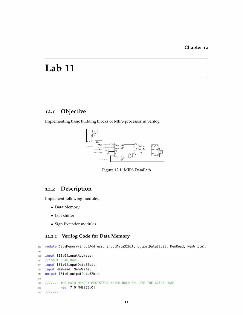
Lab 11
11.1 Objective
To implement basic building blocks of MIPs processor.
11.2 Description
MIPS datapath to be implemented is in figure 1.1.
Figure 11.1: MIPS DataPath
• The instruction memory has 128 32-bit words. Later it will be expanded. All instruc-tions and the PC are 32-bit wide. (Simply the 7 least significant bits (2ËE7 = 128) areused for the time being.)
• Implement the instruction memory, 2x1 MUX, and Incrementer-by-4 as separate mod-ules. For the time being consider that the 1-bit signal PCSrc comes from a 1-bit register,PC choose.
11.2.1 Verilog code for Multiplexer
81 module MUX_2to1( input1 , input2, select, out );82 input [31:0] input1, input2;83 input select;84 output [31:0]out;85 reg [31:0]out;86
87 always @(input1 or input2 or select )88 begin89 case(select)
30

§11.2 Description 31
90
91 1’b0: out=input1;92 1’b1: out=input2;93
94 endcase95 end96 endmodule
11.2.2 Verilog code for Adder
97 module Adder32Bit(input1, input2, out, overflowBit);98
99 input [31:0] input1, input2;100 output [31:0] out;101 reg [31:0]out;102 output overflowBit;103 reg overflowBit;104
105 always@(input1 or input2)106 begin107
108 {overflowBit , out } = input1 + input2;109
110 end111
112 endmodule
11.2.3 Verilog code for Instruction Memory
113 module InstructionMemory(readAddress, instruction);114 input [31:0]readAddress;115 output [0:31]instruction;116 reg [0:31]instruction;117
118 reg [0:7]InstructionMemory[0:31];119
120 reg [4:0]internalAddress;121
122 integer internalAddressINT, placeVal, i, j;123
124 always@(readAddress)125 begin126 //use this template to hardwire instructions.127 //Only 5 bit addresses supported.128 // InstructionMemory[0] = 32’b00000_00000_00000_00000_00000_000000;129
130 {InstructionMemory[0], InstructionMemory[1], InstructionMemory[2], InstructionMemory[3]} = 32’b001101_10010_10011_0000000000000001;//ori $s2, $s1 , 1539;
131 {InstructionMemory[4], InstructionMemory[5], InstructionMemory[6], InstructionMemory[7]} = 32’b000101_10011_00000_0000000000000100;// bne $s2, reg1, 4h;
132
133
134 {InstructionMemory[24], InstructionMemory[24+1], InstructionMemory[24+2], InstructionMemory[24+3]} = 32’b001000_10011_10010_0000000000000100;//addi $s1, $s2 ,4;

32 Lab 11
135 {InstructionMemory[28], InstructionMemory[28+1], InstructionMemory[28+2], InstructionMemory[28+3]} = 32’b000010_00000_00000_0000000000000000;// j 0;
136 // InstructionMemory[1] = 32’b001001_10010_10011_00000_00000_000010; //addi $s2, $s3, 2;137 // InstructionMemory[3] = 32’b000000_00010_00001_00000_00000_100000;138
139 //truncating the address.140 internalAddress = readAddress[4:0];141
142 //internalAddressINT = 0;143 //144 placeVal = 1;145 internalAddressINT = 0;146 for(i=0 ; i<5 ; i=i+1)147 begin148 if(internalAddress[i] == 1)149 internalAddressINT = internalAddressINT + placeVal;150
151 placeVal = placeVal * 2;152 end153
154
155 for(i=0 ; i<32 ; i=i+1)156 begin157 instruction[i] = InstructionMemory[internalAddressINT + i/8][i\%8];158 end159
160
161 end162
163 endmodule
11.3 Tasks for Students
Write testbenches to verify above blocks and attach waveforms.
Chapter 12
Lab 11
12.1 Objective
Implementing basic building blocks of MIPS processor in verilog.
Figure 12.1: MIPS DataPath
12.2 Description
Implement following modules.
• Data Memory
• Left shifter
• Sign Extender modules.
12.2.1 Verilog Code for Data Memory
164 module DataMemory(inputAddress, inputData32bit, outputData32bit, MemRead, MemWrite);165
166 input [31:0]inputAddress;167 //input READ_Bar;168 input [31:0]inputData32bit;169 input MemRead, MemWrite;170 output [31:0]outputData32bit;171
172 /////// THE MAIN MEMORY REGISTERS WHICH HOLD EMULATE THE ACTUAL RAM.173 reg [7:0]MM[255:0];174 ///////
33

34 Lab 11
175
176 reg [7:0]address;177 reg [7:0]dataBuff;178 reg [31:0]outputData32bit;179
180 integer addressInt, i, j, placeVal,var, baseAddress;181 genvar k;182
183 always @( inputData32bit or inputAddress or MemRead or MemWrite)184 begin185
186 address=inputAddress[7:0];187
188 //calculating address as an integer189
190 addressInt = 0; // the integer equivalent of the 8 bit address we have got in the address[]191 placeVal = 1; // the placevalue for the unit place is 1.192
193 for( i=0 ; i<8 ; i=i+1 )194 begin195
196 if(address[i] == 1’b1)197 addressInt = addressInt + placeVal;198
199 placeVal = placeVal * 2;200 end201
202 //calculated address as an integer, stored in addressInt203
204
205
206 if(MemRead == 1) // the memory is being read from.207 begin208
209 baseAddress = addressInt; // i is the variable pointing to the address location pointed by the input address210
211 // now copying the 8 bits of the pointed address one by one.212
213 ///BIG ENDIAN214 for(i=0 ; i<4 ; i=i+1)215 begin216 for(j = 0 ; j < 8 ; j = j+1 )217 begin218 outputData32bit[j] = MM[baseAddress + i][j];219 end220 end221
222
223
224 end //End of readbar condition 1225
226
227
228 if(MemWrite == 1) // the memory is being written into

§12.2 Description 35
229 begin230 baseAddress = addressInt;231
232 // the given data is being written into the place pointed by the address233
234 ///BIG ENDIAN235 for(i=0 ; i<4 ; i = i + 1)236 begin237
238 for(j = 0 ; j < 8 ; j = j+1 )239 begin240 MM[baseAddress + i][j] = inputData32bit[j] ;241 end242
243 end244
245
246 end // End of data writing block247
248
249
250 end // end of the always block251 endmodule
12.2.2 Verilog code for Left Shifter
253 module LeftShifter_2bit(inData,outData);254
255 input [31:0]inData;256 output [31:0]outData;257 reg [31:0]outData;258
259 always@(inData)260 begin261
262 outData=inData<<2;263
264 end265
266 endmodule
12.2.3 Verilog code for Sign Extention
267 module SignExtender_16to32(inputData, outputData);268
269 input[15:0] inputData;270 output[31:0] outputData;271 reg [31:0] outputData;272
273 always@(inputData)274 begin275
276 outputData[15:0] = inputData[15:0];277 outputData[31:16] = {16{inputData[15]}};278

36 Lab 11
279 end280 endmodule
12.3 Tasks for Students
Write testbenches to verify above blocks and attach waveforms.

Chapter 13
Lab 13
13.1 Objective
Implementing basic building blocks of MIPS processor in verilog.
Figure 13.1: MIPS DataPath
13.2 Description
Implement following modules.
• Register File
• ALU
13.2.1 Verilog Code for Register File
281 module RegisterFile(readReg1, readReg2, writeReg, writeData, readData1, readData2, RegWrite);282 input [4:0]readReg1, readReg2, writeReg;283 input [31:0]writeData; //address of the register to be written on to.284 input RegWrite; //RegWrite - register write signal; writeReg-the destination register.285
286 output [31:0]readData1, readData2;287 reg [31:0]readData1, readData2;288
289 reg [31:0]RegMemory[0:31];290
291 integer placeVal, i, j, writeRegINT=0, readReg1INT=0, readReg2INT=0;292
293 initial
37

38 Lab 13
294 begin295 for(i=0 ; i<32 ; i=i+1)296 begin297 for(j=0 ; j<32 ; j= j+1)298 RegMemory[i][j] = 1’b0;299 end300 end301
302 always@ (RegWrite or readReg1 or readReg2 or writeReg or writeData)303 begin304
305 if(RegWrite == 1)306 begin307
308 placeVal = 1;309 readReg1INT=0;310 readReg2INT=0;311 for(i=0 ; i<5 ; i=i+1)312 begin313 if(readReg1[i] == 1)314 readReg1INT = readReg1INT + placeVal;315
316 if(readReg2[i] == 1)317 readReg2INT = readReg2INT + placeVal;318
319 placeVal = placeVal * 2;320 end321
322
323 for(i=0 ; i<32 ; i=i+1)324 begin325 readData1[i] = RegMemory[readReg1INT][i];326 readData2[i] = RegMemory[readReg2INT][i];327 end328
329
330
331 //binary to decimal address translation.332 placeVal = 1;333 writeRegINT=0;334 for(i=0 ; i<5 ; i=i+1)335 begin336 if(writeReg[i] == 1)337 writeRegINT = writeRegINT + placeVal;338
339 placeVal = placeVal * 2;340 end341
342 $display("before writing %d at %d", writeData, writeRegINT);343 for(i=0 ; i<32 ; i=i+1)344 begin345 RegMemory[writeRegINT][i] = writeData[i];346 end347 $display("after writing %d at %d", writeData, writeRegINT);

§13.2 Description 39
348
349 end // Register Write350
351 if(RegWrite == 0)352 begin353 //binary to decimal address translation.354 placeVal = 1;355 readReg1INT=0;356 readReg2INT=0;357 for(i=0 ; i<5 ; i=i+1)358 begin359 if(readReg1[i] == 1)360 readReg1INT = readReg1INT + placeVal;361
362 if(readReg2[i] == 1)363 readReg2INT = readReg2INT + placeVal;364
365 placeVal = placeVal * 2;366 end367
368
369 for(i=0 ; i<32 ; i=i+1)370 begin371 readData1[i] = RegMemory[readReg1INT][i];372 readData2[i] = RegMemory[readReg2INT][i];373 end374
375
376 end// Register Read377
378 end //always@379
380 endmodule
13.2.2 Verilog code for ALU
381 module ALU_Core(ALUSrc1 , ALUSrc2 , ALUCtrl , ALUResult , Zero);382 input[31:0] ALUSrc1;383 input[31:0] ALUSrc2;384 input[2:0] ALUCtrl;385
386 output Zero;387 reg Zero;388
389 output [31:0]ALUResult;390 reg [31:0]ALUResult;391
392
393 always @(ALUSrc1 or ALUSrc2 or ALUCtrl)394 begin395
396 if(ALUCtrl == 3’b010) //’add’397 begin398 ALUResult = ALUSrc1 + ALUSrc2;399 if(ALUResult == 32’h0000)

40 Lab 13
400 begin401 Zero = 1’b1;402 end403 else404 begin405 Zero = 1’b0;406 end407 end408
409 if(ALUCtrl == 3’b110) // ’sub’410 begin411 ALUResult = ALUSrc1 - ALUSrc2;412 if(ALUResult == 32’h0000)413 begin414 Zero = 1’b1;415 end416 else417 begin418 Zero = 1’b0;419 end420 end421
422 if(ALUCtrl == 3’b000) // ’and’423 begin424 ALUResult = ALUSrc1 & ALUSrc2;425 if(ALUResult == 32’h0000)426 begin427 Zero = 1’b1;428 end429 else430 begin431 Zero = 1’b0;432 end433 end434
435 if(ALUCtrl == 3’b001) // ’or’436 begin437 ALUResult = ALUSrc1 | ALUSrc2;438 if(ALUResult == 32’h0000)439 begin440 Zero = 1’b1;441 end442 else443 begin444 Zero = 1’b0;445 end446 end447
448 if(ALUCtrl == 3’b111) // ’slt’449 begin450 ALUResult = ALUSrc1 - ALUSrc2;451 if(ALUResult == 32’h0000)452 begin453 Zero = 1’b1;

§13.3 Tasks for Students 41
454 end455 else456 begin457 Zero = 1’b0;458 end459 end460
461 end462
463 endmodule464
465
466
467 module ALU_Control(FunctField, ALUOp, ALUCtrl);468 input [5:0]FunctField;469 input [1:0]ALUOp;470 output [2:0]ALUCtrl;471 reg [2:0]ALUCtrl;472
473 always@(FunctField or ALUOp)474 begin475 if(ALUOp == 2’b10) //’Arithmetic’ Type Instructions476 begin477 case(FunctField)478 //begin479 6’b100000: ALUCtrl = 3’b010; //ADDITION in ’R’ Type480 6’b100010: ALUCtrl = 3’b110; //SUBTRACTION in ’R’ Type481 6’b100100: ALUCtrl = 3’b000; //AND in ’R’ Type482 6’b100101: ALUCtrl = 3’b001; //OR in ’R’ Type483 6’b101010: ALUCtrl = 3’b111; //SLT in ’R’ Type484 // end485 endcase486 end487
488 if(ALUOp == 2’b00) // ’LW/SW’ Type Instructions489 begin490 ALUCtrl = 3’b010; //ADDITION irrespective of the FunctField.491 end492
493 if(ALUOp == 2’b01) // ’BEQ’, ’BNE’ Type Instructions494 begin495 ALUCtrl = 3’b110; //SUBTRACTION irrespective of the FunctField.496 end497
498
499
500 end //always block501
502 endmodule //ALUOp module
13.3 Tasks for Students
Write testbenches to verify above blocks and attach waveforms.

Chapter 14
Lab 13
14.1 Objective
integrating previusely developed basic building blocks of MIPS processor.
Figure 14.1: MIPS DataPath
14.2 Description
Connect the modules in a seprate module and run basic level testing using testbench.
14.2.1 Verilog Code for Complete Processor
503 module SingleCycleMain(initialPCval, run);504 input [31:0]initialPCval;505 input run;506
507 reg [31:0]PC;508
509
510 //instances of all the smaller modules of the processor.511
512 reg [31:0]instrReg;513
514 reg [31:0]instrAddress;515 wire [31:0]instrWire;516 InstructionMemory instrMem(instrAddress, instrWire);517
518 reg [31:0]inputToShiftLeft;519 wire [31:0]outputFromShiftLeft;
42

§14.2 Description 43
520 LeftShifter_2bit instLftShft(inputToShiftLeft, outputFromShiftLeft);521
522 //reg [31:0]PC; //already declared523 reg [31:0]constantFour;524 wire [31:0]nextPCval;525 wire overflow1;526 Adder32Bit nextPCvalue(PC, constantFour, nextPCval, overflow1);527
528 // wire [31:0]nextPCval;529 // wire [31:0]outputFromShiftLeft;530 wire [31:0]nextPCvalPlusOffset;531 wire overflow2;532 Adder32Bit PCafterBranch(nextPCval, outputFromShiftLeft, nextPCvalPlusOffset, overflow2);533
534 reg [31:0]dataAddress;535 reg [31:0]inputData;536 wire[31:0]outputData;537 reg MemRead, MemWrite;538 DataMemory dataMem(dataAddress, inputData, outputData, MemRead, MemWrite);539
540
541 reg [4:0]inputReg1;542 reg [4:0]inputReg2;543 reg RegDst;544 wire [4:0]writeRegWire;545 MUX_2to1_5bit regDstMUX(inputReg1, inputReg2, RegDst, writeRegWire);546
547
548 reg [4:0]readReg1, readReg2, writeReg;549 reg [31:0]writeData;550 wire [31:0]readData1, readData2;551 reg RegWrite;552 RegisterFile regFile(readReg1, readReg2, writeReg, writeData, readData1, readData2, RegWrite);553
554
555 reg [15:0]inputDataSEXT;556 wire [31:0]outputDataSEXT;557 SignExtender_16to32 signExt(inputDataSEXT, outputDataSEXT);558
559
560 //wire [31:0]readData2; //already declared.561 //wire [31:0]outputDataSEXT; //already declared.562 reg aluSrc;563 wire [31:0] ALUSrc2;564 MUX_2to1 aluSrc2MUX(readData2, outputDataSEXT, aluSrc, ALUSrc2);565
566
567 reg [5:0]FunctField;568 reg [1:0]ALUOp;569 wire [2:0]ALUCtrl1;570 ALU_Control aluCtrlInstance(FunctField, ALUOp, ALUCtrl1);571
572
573 reg [31:0]ALUSrc1;

44 Lab 13
574 //wire [31:0] ALUSrc2;575 reg [2:0]ALUCtrl;576 wire[31:0]ALUout;577 wire ZeroOUT;578 ALU_Core aluCoreInstance(ALUSrc1, ALUSrc2, ALUCtrl, ALUout, ZeroOUT);579
580 reg Branch;581 reg ZeroIN;582 wire BranchEnabled;583 and branchAND(BranchEnabled, Branch, ZeroIN);584
585
586 // wire [31:0]nextPCval;587 // wire [31:0]nextPCvalPlusOffset;588 // wire BranchEnabled;589 wire [31:0]nextPCactual;590 MUX_2to1 pcSrcMUX(nextPCval, nextPCvalPlusOffset, BranchEnabled, nextPCactual);591
592
593 //wire[31:0]ALUout; //already declared594 //wire[31:0]outputData; //already declared595 reg MemtoReg;596 wire [31:0]writeDataToReg;597 MUX_2to1 mem2regSrcMUX(ALUout, outputData, MemtoReg, writeDataToReg);598
599
600 //Requisite Datastructures for manipulation.601 reg [5:0]OpCode;602 reg [4:0]rs, rt, rd, shamt;603 reg [25:0]target;604 reg [31:0]jumpTarget;605 integer counter, prevInstrWasJ;606
607 initial608 begin609 PC = initialPCval;610 //instrReg = 32’b001001_10010_10011_00000_00000_000100; //addi $s1, $s2 ,4;611 constantFour = 32’h0000_0004; //updated it was ’constantFout’612 counter = 0;613 end614
615 always@(run) //this will make it work like trace. to make the execution sequential & automatic use always(PC)616 begin617 if(counter != 0) //that is if we are not executing for the first time, we will not take the previously calculated pc value.618 PC = nextPCactual;619
620 if(prevInstrWasJ == 1) //that is if the previous instruction was jump, take next pc from a specified collection register.621 PC = jumpTarget;622
623 instrAddress = PC;624 #10625 instrReg = instrWire; //updated, this link was not there.626 //Now the wire instrReg has the Instruction corresponding to this PC.627 OpCode = instrReg[31:26];
§14.2 Description 45
628
629 writeReg = 5’b00000;630 writeData = 32’h1111_1111;631
632 RegDst = 0;633 $display("value after init, %d, %d", writeReg, writeRegWire);634
635 counter = 1; //to keep track of the fact that we are not executing our first instruction.636
637 /* Beginning of ##CRITICAL INTERCONNECTIONS##. DO NOT MODIFY*/638 rs = instrReg[25:21];639 rt = instrReg[20:16];640 rd = instrReg[15:11];641 inputDataSEXT = instrReg[15:0];642 shamt = instrReg[10:6];643 FunctField = instrReg[5:0];644
645
646 //the inputs to the register file.647 readReg1 = rs;648 readReg2 = rt;649
650 //the two inputs to the RegDst mux.651 inputReg1 = rt;652 inputReg2 = rd;653 #10654 //$display("value of writeRegWire after input1 input2, %d", writeRegWire);655
656 //now the output of the register file should be correctly assigned to aluSrc1 and aluSrcMux1.657
658
659 //#50660 //$display("before value of ALUSrc1, readData1 %d %d", ALUSrc1, readData1);661 //ALUSrc1 = readData1;662 //$display("after value of ALUSrc1, readData1 %d %d", ALUSrc1, readData1);663 //ALUSrc2_input1 = readData2; this has been already hardwired.664 //ALUSrc2_input2 = outputDataSEXT; this has been already hardwired.665
666 //output from ALUControl being passed into ALUCore.667 ALUCtrl = ALUCtrl1;668
669 //now the output of the mux needs to be redirected to the writeReg of the register file670 // #10671 //writeReg = writeRegWire;672 $display("value after first mod, %5d, %5s", writeReg, writeRegWire);673 //connecting ALUout with memory input and memory mux.674 //ALUout already connected to mem2regMUX.675 dataAddress = ALUout;676 ZeroIN = ZeroOUT; //ALU connections complete677
678
679 //connecting the readData2 register output to the memory data input.680 inputData = readData2;681 //the outputData is already connected to the mem2regMUX.

46 Lab 13
682
683 //output from Sign extender being given to the shiftleft module.684 inputToShiftLeft = outputDataSEXT;685 #20686 //now we need to check if the memory mux output is connected to the writeData of regFile.687 //writeData = writeDataToReg;688
689
690
691 /* End of ##CRITICAL INTERCONNECTIONS##. DO NOT MODIFY*/692
693
694
695
696
697
698
699 if(OpCode == 6’b000010 || OpCode == 6’b000011) //If the instruction is ’J’ type.700 begin701 target = instrReg[25:0];702 jumpTarget[27:2] = target;703 jumpTarget[1:0] = 2’b00;704 jumpTarget[31:28] = PC[31:28];705 prevInstrWasJ = 1;706 end707
708 else if(OpCode == 6’b000000) // If the instruction is ’R’ type.709 begin710
711 ALUOp = 2’b10;712 RegDst = 1’b1;713 Branch = 0;714 MemRead = 0;715 MemWrite = 0;716 aluSrc = 0;717 MemtoReg = 0;718 RegWrite = 1;719
720
721 end //’R’ Type.722
723
724 else // If the instruction is ’I’ type.725 begin726
727
728 if(OpCode == 6’b100011) // lw instruction.729 begin730 //Control Signals731 ALUOp = 2’b00;732 RegDst = 1’b0;733 Branch = 0;734 MemRead = 1;735 MemWrite = 0;

§14.2 Description 47
736 aluSrc = 1;737 MemtoReg = 1;738 RegWrite = 1;739
740 end741
742 if(OpCode == 6’b101011) //sw instruction743 begin744 //Control Signals745 ALUOp = 2’b00;746 RegDst = 1’b0; //irrelevant as data not being written into regfile.747 Branch = 0;748 MemRead = 0;749 MemWrite = 1;750 aluSrc = 1;751 MemtoReg = 1; //irrelevant752 RegWrite = 0;753
754 end755
756 if(OpCode == 6’b000100) //beq instruction757 begin758 //Control Signals759 ALUOp = 2’b01;760 RegDst = 1’b0; //irrelevant761 Branch = 1;762 MemRead = 0;763 MemWrite = 0;764 aluSrc = 0;765 MemtoReg = 1; //irrelevant766 RegWrite = 0; //irrelevant767
768 end769
770 if(OpCode == 6’b000101) //bne instruction771 begin772 //Control Signals773 ALUOp = 2’b01; //for branch instruction.774 RegWrite = 0;775 RegDst = 0;776 Branch = 1;777 aluSrc = 0;778 ZeroIN = ~ZeroOUT; //passing the negated value of ZeroOUT from the ALU to the PCSrc MUX.779 MemRead = 0;780 MemWrite = 0;781
782 MemtoReg = 1;783
784
785
786
787
788 end789

48 Lab 13
790 if(OpCode == 6’b001101) //ori instruction791 begin792
793 //Control Signals794 prevInstrWasJ = 0;795 ALUOp = 2’b01; //presently irrelevant796 RegDst = 0;797
798 Branch = 0;799 MemRead = 0;800 MemWrite = 0;801 //now the output of the mux needs to be redirected to the writeReg of the register file802 $display("value after first mod before second,\%5d, \%5d", writeReg, writeRegWire);803 writeReg = writeRegWire;804 $display("value after second mod,\%5d, \%5d", writeReg, writeRegWire);805 RegWrite=1;806
807
808 #50809 $display("value of readData1, \%d", readData1);810
811 #50812 $display("value of readData1, \%d", readData1);813 ALUSrc1 = readData1;814 aluSrc = 1;815
816 ALUCtrl = 3’b001; //for or817 #20818
819 $display("1 writeData = \%d, writeDataToReg =\%d", writeData, writeDataToReg);820
821 MemtoReg = 0; //the aluout is to be redirected to the regwrite.822 #20823 $display("2 writeData = \%d, writeDataToReg = \%d", writeData, writeDataToReg);824
825 writeData = writeDataToReg;826 RegWrite = ~RegWrite; //this will write the initialized value 32’b1111_1111827 RegWrite = ~RegWrite; //this will run the next cycle of the reg file, writing the updated value.828
829 $display("3 writeData = \%d, writeDataToReg = \%d", writeData, writeDataToReg);830
831
832
833
834 end835
836 if(OpCode == 6’b001000) //addi instruction837 begin838 //Control Signals839 prevInstrWasJ = 0;840 ALUOp = 2’b01; //presently irrelevant841 RegDst = 0;842
843 Branch = 0;

§14.3 Tasks for Students 49
844 MemRead = 0;845 MemWrite = 0;846 //now the output of the mux needs to be redirected to the writeReg of the register file847 $display("value after first mod before second,\%5d, \%5d", writeReg, writeRegWire);848 writeReg = writeRegWire;849 $display("value after second mod,\%5d, \%5d", writeReg, writeRegWire);850 RegWrite = 1;851
852 #20853 $display("value of readData1, \%d", readData1);854 ALUSrc1 = readData1;855 aluSrc = 1;856
857 ALUCtrl = 3’b010; //for add858 #20859
860 $display("1 writeData = \%d, writeDataToReg = \%d", writeData, writeDataToReg);861
862 MemtoReg = 0; //the aluout is to be redirected to the regwrite.863 #20864 $display("2 writeData = \%d, writeDataToReg = \%d", writeData, writeDataToReg);865
866 writeData = writeDataToReg;867 RegWrite = ~RegWrite;868 RegWrite = ~RegWrite;869
870 $display("3 writeData = \%d, writeDataToReg = \%d", writeData, writeDataToReg);871
872 end873
874 end //’I’ Type.875
876
877 end //always block878
879
880 endmodule
14.3 Tasks for Students
Write testbenches to verify above blocks and attach waveforms.