Embed Size (px)
Citation preview

|''|''|||''|'''|||'|
III B.Tech II Semester Regular/Supplementary Examinations, May/June - 2015
COMPUTER NETWORKS
(Comm to ECE and ECM)
Time: 3 hours Max. Marks: 75
Answer any FIVE Questions
All Questions carry equal marks
*****
1 a) What is network architecture? What is layered architecture? Explain design issues for
the layers
[9]
b) Explain about ATM reference model
[6]
2 Explain unguided transmission media in detail
[15]
3 a) Explain elementary data link layer protocols [9]
b) Calculate the polynomial checksum for the following frame and generator
Frame: 1001010011and Generator: x5+x+1
[6]
4 Explain different carrier sense multiple access protocols in detail
[15]
5 a) What is network layer? Explain the design issues of network layer [7]
b) What is a routing algorithm? Explain the classification of routing algorithms
[8]
6 a) What is congestion? Explain the general principles of congestion control [6]
b) What is fragmentation? Explain transparent and non-transparent fragmentation in
network layer
[9]
7 a) Explain Transport layer services in detail [6]
b) Explain UDP header format and UDP applications
[9]
8 a) Explain HTTP protocol in detail. Write in detail about get and post methods. [8]
b) Explain briefly about multi media content. [7]
-000-
Code No: R32041 Set No. 1 R10

|''|''|||''|'''|||'|
III B.Tech II Semester Regular/Supplementary Examinations, May/June - 2015
COMPUTER NETWORKS
(Comm to ECE and ECM)
Time: 3 hours Max. Marks: 75
Answer any FIVE Questions
All Questions carry equal marks
*****
1 Explain OSI reference model and compare it with TCP/IP. [15]
2 Explain guided transmission media in detail. [15]
3 a) Explain HDLC protocol in detail. [9]
b) Compare and contrast byte oriented and bit oriented protocols.
[6]
4 a) Explain dynamic channel allocation methods in detail. [7]
b) Explain the architecture of BLUETOOTH.
[8]
5 a) List the differences between Virtual circuits and data gram subnets. [7]
b) Explain the shortest path routing algorithm.
[8]
6 a) Explain how networks are differ by their topology. [6]
b) What is internetworking? Explain tunneling in detail.
[9]
7 a) Explain the connection management in TCP. [7]
b) Explain ATM AAL layer protocol.
[8]
8 a) Explain the DNS Name Space and DNS protocol. [9]
b) Explain basic functions of e-mail systems. [6]
-000-
Code No: R32041 Set No. 2 R10
|''|''|||''|'''|||'|
III B.Tech II Semester Regular/Supplementary Examinations, May/June - 2015
COMPUTER NETWORKS
(Comm to ECE and ECM)
Time: 3 hours Max. Marks: 75
Answer any FIVE Questions
All Questions carry equal marks
*****
1 a) What is internet? Explain birth of internet. [6]
b) Explain different network topologies.
[9]
2 a) What is switching? Explain different methods of switching in detail. [9]
b) Explain the difference between Narrow band and Broad band ISDN.
[6]
3 a) Explain different framing techniques used in data link layer. [10]
b) Compare and contrast flow and error control.
[5]
4 a) Explain CSMA/CD protocol. [7]
b) Explain MAC sub layer of IEEE802.11 standard.
[8]
5 a) Explain store and forward and Sink tree concept. [7]
b) Explain flooding algorithm and its applications.
[8]
6 a) What is congestion? Explain the congestion prevention polices. [6]
b) Explain Broad cast routing algorithm.
[9]
7 a) Compare the UDP and TCP. [6]
b) Explain TCP Segment format.
[9]
8 a) Explain the Network Security model. [7]
b) Explain SMTP and its drawbacks? Explain advantage of MIME. [8]
-000-
Code No: R32041 Set No. 3 R10

|''|''|||''|'''|||'|
III B.Tech II Semester Regular/Supplementary Examinations, May/June - 2015
COMPUTER NETWORKS
(Comm to ECE and ECM)
Time: 3 hours Max. Marks: 75
Answer any FIVE Questions
All Questions carry equal marks
*****
1 Explain TCP/IP reference model and compare it with OSI reference model. [15]
2 Explain the following encoded techniques and draw the signal waveform when
10110101 is transmitted
a) NRZ encoding
b) Manchester encoding
c) Differential Manchester Encoding
[15]
3 a) Explain data link design issues in detail. [7]
b) Briefly explain Hamming error detection and correcting code with example.
[8]
4 a) Explain ALOHA protocols in detail. [8]
b) Explain IEEE 802.3 Frame format.
[7]
5 a) Explain distance vector routing algorithm with suitable example. [7]
b) What is count to infinity problem? Explain.
[8]
6 a) Explain load shedding congestion control algorithm. [5]
b) Explain the congestion control in datagram subnets.
[10]
7 a) Explain TCP features. [5]
b) What is silly Window Syndrome? Explain how the problem created at sender and
receiver side? Give the solution to both the sides.
[10]
8 a) What is WWW? Explain in detail about Dynamic Web pages. [8]
b) Briefly explain about SNMP. [7]
-000-
Code No: R32041 Set No. 4 R10

|''|''|||''|'''|||'|
III B.Tech II Semester Regular/Supplementary Examinations, May/June - 2015
DIGITAL SIGNAL PROCESSING
(Comm to ECE and ECM)
Time: 3 hours Max. Marks:75
Answer any FIVE Questions
All Questions carry equal marks
*****
1 a) Define various elementary discrete time signals. Write notes on them and explain about
their properties.
[8]
b) Determine whether the following systems are time invariant or not
a)y[n]=x[n]+nx[n-3] b)y[n]=sin(x[n]).
[7]
2 a) State and prove the convolution theorem using DFT. [8]
b) Find the linear convolution of two sequences 1,0,2 and 1,1 using DFT.
[7]
3 a) An 8 point sequence is given by x[n]=2,2,2,2,1,1,1,1 Find the DFT of the sequence
using direct computation.
[9]
b) Develop a radix-3 DIT FFT algorithm for evaluating the DFT for N=9.
[6]
4 a) Discuss about different methods of realization of IIR systems and explain how the
conversion can be made from direct form-I structure to direct form-II structure.
[8]
b) Find the step response of the system whose impulse response is given by h(n)=a-n
u(-n),
0<a<1.
[7]
5 a) Convert the following transfer function into digital filter using backward difference
operator,2)5.0(16
3)(
++=
ssH
[8]
b) Explain about Frequency warping effect and suggest a remedy for it.
[7]
6 a) Find and explain the frequency responses of rectangular and Hanning windows. [8]
b) Design a Linear phase low pass FIR filter with a cutoff frequency of π/2 rad/sec using
frequency sampling technique. Take N=13.
[7]
7 a) Define sampling. What is a down sampling operation and discuss about the Frequency
response of a down sampling operation.
[8]
b) Define a ramp sequence and sketch its interpolated and decimated versions with a
factor of 3.
[7]
8 Write short notes on the following
a) Multiplier and Accumulator [8]
b) Special addressing modes of dsp processors. [7]
-000-
Code No: R32043 Set No. 1 R10

|''|''|||''|'''|||'|
III B.Tech II Semester Regular/Supplementary Examinations, May/June - 2015
DIGITAL SIGNAL PROCESSING
(Comm to ECE and ECM)
Time: 3 hours Max. Marks: 75
Answer any FIVE Questions
All Questions carry equal marks
*****
1 a) Check whether the following systems are linear or not
i)y[n]=n2x[n] ii)y[n]=2x[n]+3
[8]
b) Define a signal. Classify them with an example. [7]
2 a) Derive the relationship between DFT and z Transform. [8]
b) What is a twiddle factor? List out some of its properties. Explain the matrix
representation of DFT and IDFT using twiddle factor.
[7]
3 a) Explain the radix-2 DIT FFT algorithm and draw the butterfly diagram for 8-point
DIT FFT.
[10]
b) Compare DIT and DIF FFT algorithms.
[5]
4 a) Compare FIR and IIR systems. [5]
b) Find the canonic forms of the system defined by the equation y[n]=x[n]-0.3x[n-1]-
0.7x[n-2]+0.6y[n-1]+0.8y[n-2].
[10]
5 a) Design a chebyshev filter using Bilinear Transformation to meet the following
specifications ππ
π
24.01.0)(
1.001)(3.0
≤≤≤
≤≤≤≤
wwH
wwH
[8]
b) Compare chebyshev and Butterworth approximations.
[7]
6 a) Show that the magnitude response of FIR system is symmetric when impulse response
is symmetric and N is odd.
[8]
b) Design a FIR low pass filter with N=7 and cutoff frequency of π/4 rad/sec.
[7]
7 a) A signal is defined as x[n] = sin (πn). Draw the original, interpolated and decimated
signals by a factor of 3.
[8]
b) Draw the block diagram of an Interpolator. Derive and Discuss about its frequency
response characteristics.
[7]
8 a) With a neat sketch explain the Internal architecture of TMS320C5X Processors. [9]
b) Explain about various addressing modes of a processor. [6]
-000-
Code No: R32043 Set No. 2 R10

|''|''|||''|'''|||'|
III B.Tech II Semester Regular/Supplementary
DIGITAL SIGNAL PROCESSING
Time: 3 hours
Answer any FIVE Questions
All Questions carry equal marks
1 a) Determine whether the following signals
i)y[n]=8x[n-4] ii)x[n]=2-n
u[n] iii)y[n]=x
b) What are the different operations that can be performed on a
with an example.
2 a) State and prove linearity, time shifting,
b) A sequence is defined as x[n] =
3 a) With a neat derivation explain the procedure to compute IDFT using Radix
b) Find the IDFT of the following sequence using DIT FFT of the
-j2, 2, j2.
4
a) Obtain the direct form I and II structures for the IIR System,
b) Discuss about the basic elements used to construct the block diagram of a discrete time
system.
5 a) Design a Butterworth Low pass filter
π ≤≤
≤≤≤≤
wwH
wwwH
3.018.0)(
01)(89.0
b) Compare analog and digital filters. State the advantages of digital filters over the analog
filters.
6 a) Compare various windows used in the design of FIR filters
b) Design a low pass FIR filter with N=
1ms using Fourier series method.
7 a) Consider a signal x[n]=1,3,2,5,4,
down sampler and I up sampler is interchangeable only if D and I are co
b) Explain about poly phase decomposition of FIR filters.
8 a) What are programmable DSPs? Classify them
over conventional microprocessors.
b) Explain the VLIW architecture with its block diagram. State the advantages and
disadvantages of VLIW architecture.
Regular/Supplementary Examinations, May/June
DIGITAL SIGNAL PROCESSING
(Comm to ECE and ECM)
Max. Marks:
Answer any FIVE Questions
All Questions carry equal marks
*****
Determine whether the following signals are stable or not
u[n] iii)y[n]=x2[n-2]
What are the different operations that can be performed on a sequence? Explain them
State and prove linearity, time shifting, and symmetry properties of DFS.
n] = 1,-1,2,-2,3,-3. Find the DFT.
With a neat derivation explain the procedure to compute IDFT using Radix-
Find the IDFT of the following sequence using DIT FFT of the sequence X(k)
Obtain the direct form I and II structures for the IIR System,57
34)(
z
zzH
+
++=
Discuss about the basic elements used to construct the block diagram of a discrete time
Design a Butterworth Low pass filter to meet the following specifications
π
π
≤w
w 2.0
Compare analog and digital filters. State the advantages of digital filters over the analog
various windows used in the design of FIR filters.
Design a low pass FIR filter with N=5, cutoff frequency of 200Hz and sampling time as
series method.
Consider a signal x[n]=1,3,2,5,4,-1,-2,6,-3,7,8,9…… Show that the cascade of D
down sampler and I up sampler is interchangeable only if D and I are co-prime.
phase decomposition of FIR filters.
What are programmable DSPs? Classify them. State the advantages of DSP processor
over conventional microprocessors.
Explain the VLIW architecture with its block diagram. State the advantages and
disadvantages of VLIW architecture.
-000-
May/June - 2015
Max. Marks: 75
[8]
Explain them [7]
[8]
[7]
-2 FFT. [8]
sequence X(k) = 6, [7]
2
22
z
z
+
+ [8]
Discuss about the basic elements used to construct the block diagram of a discrete time [7]
[10]
Compare analog and digital filters. State the advantages of digital filters over the analog [5]
[7]
cutoff frequency of 200Hz and sampling time as [8]
the cascade of D
prime.
[8]
[7]
. State the advantages of DSP processor [6]
Explain the VLIW architecture with its block diagram. State the advantages and [9]

|''|''|||''|'''|||'|
III B.Tech II Semester Regular/Supplementary Examinations, May/June - 2015
DIGITAL SIGNAL PROCESSING
(Comm to ECE and ECM)
Time: 3 hours Max. Marks: 75
Answer any FIVE Questions
All Questions carry equal marks
*****
1 a) Define stability of a system. Explain about BIBO stability criterion of a discrete
system.
[8]
b) i)Draw the even and odd parts of the following signals x[n]=5,4,3,2,1
ii)Check u[n]-u[n-6] is a power signal or not
[7]
2 a) Define DFS of a sequence and explain about exponential form and trigonometric
forms. Derive the relation between two types of representations.
[8]
b) A signal is defined as x[n]=1,2,3,-1,-2 Find the exponential form of DFS.
[7]
3 a) A sequence is given by x[n]=1,2,3,4,4,3,2,1 Compute the 8-point DFT of x[n] by
using radix-2 DIT FFT algorithm.
[8]
b) Develop a DIF FFT algorithm for decomposing the DFT for N=3X2.
[7]
4 a) What is an IIR system? Explain about Direct Form I and II structures for the IIR
systems and also compare them.
[8]
b) Realize the following transfer function using Direct Form II structure
H(z)=1+0.25z-1
+0.75z-2
[7]
5 a) Discuss about characteristics of analog Butterworth low pass filter and give its pole
locations. Discuss about pole locations of digital chebyshev filter.
[8]
b) Determine the order and the poles of the low pass Butterworth filter that has -3dB
bandwidth of 500Hz and an attenuation of 40dB at 1000Hz.
[7]
6 a) Design an FIR low pass filter using Hanning windows with pass band gain of 1dB,
cutoff frequency of 400Hz, sampling frequency of 1 kHz. Assume the length of the
impulse response as 7.
[9]
b) Compare Hanning and Hamming windows
[6]
7 a) Consider a sequence x[n]=anu[n]. i) Determine the spectrum of the signal. ii) The
signal is applied to a decimator that reduces the sampling rate by a factor 2. Determine
the output spectrum.
[8]
b) Explain any two applications of Multi Rate signal processing
[7]
8 a) Explain various interrupt structures supported by TMS320C5X Processor. [8]
b) What are the various on chip peripherals available in TMS320C5X Processor?
Explain any two of them.
[7]
-000-
Code No: R32043 Set No. 4 R10

|''|''|||''|'''|||'|
III B.Tech II Semester Regular/ Supplementary Examinations, May/June - 2015
MANAGEMENT SCIENCE (Common to EEE, ECE, CSE, CHEM, EIE, BME, IT)
Time: 3 hours Max. Marks: 75
Answer any FIVE Questions
All Questions carry equal marks
*****
1 a) What is the significance of Hawthorne experiments for management? [8]
b) Define Management and explain its functions. [7]
2 a) Explain the significance of statistics in quality control. [7]
b) Explain the variables that go into the determination of Economic Order Quantity. [8]
3 a) What do you understand by Human Resource Management? [8]
b) Define Human Resource Development? Outline its concept. [7]
4 The following table gives the information about various activities of a project
network.
The indirect cost per day is 2,600/-. Determine the optimum cost and duration of the
project.
Activity Normal
Time
Normal
Cost
Crash
Time
`Crash
Cost
1-2 9 8000 7 10000
1-3 5 5000 3 8000
2-3 7 7000 5 8600
2-4 8 6000 6 7000
3-4 6 9000 4 11400
[15]
5 a) How do you formulate and implement strategy? Explain.
[8]
b) What is the need for corporate planning process? [7]
6 a) What is Ethics? Explain the importance of ethics in financial management.
[8]
b) “Ethical financial management practices lead an organization to greater heights”
Discuss.
[7]
7 a) Briefly explain the various techniques of business communication. [8]
b) What are the problems faced while meeting the cross cultural communication? [7]
8 a) Define Total Quality Management and explain its significance. [8]
b) Write notes on six sigma. [7]
*****
Code No: R32026 Set No. 1 R10
|''|''|||''|'''|||'|
III B.Tech II Semester Regular/ Supplementary Examinations, May/June - 2015
MANAGEMENT SCIENCE (Common to EEE, ECE, CSE, CHEM, EIE, BME, IT)
Time: 3 hours Max. Marks: 75
Answer any FIVE Questions
All Questions carry equal marks
*****
1 a) Explain the nature and importance of management. [8]
b) What are the challenges you have to face as a manager?
[7]
2 a) Describe the basic procedure to be followed in adopting work study techniques for
Sound results.
[8]
b) What is inventory? Explain the need for inventory control.
[7]
3 a) Explain the functions of personnel management. [8]
b) Evaluate the different sources of recruitment.
[7]
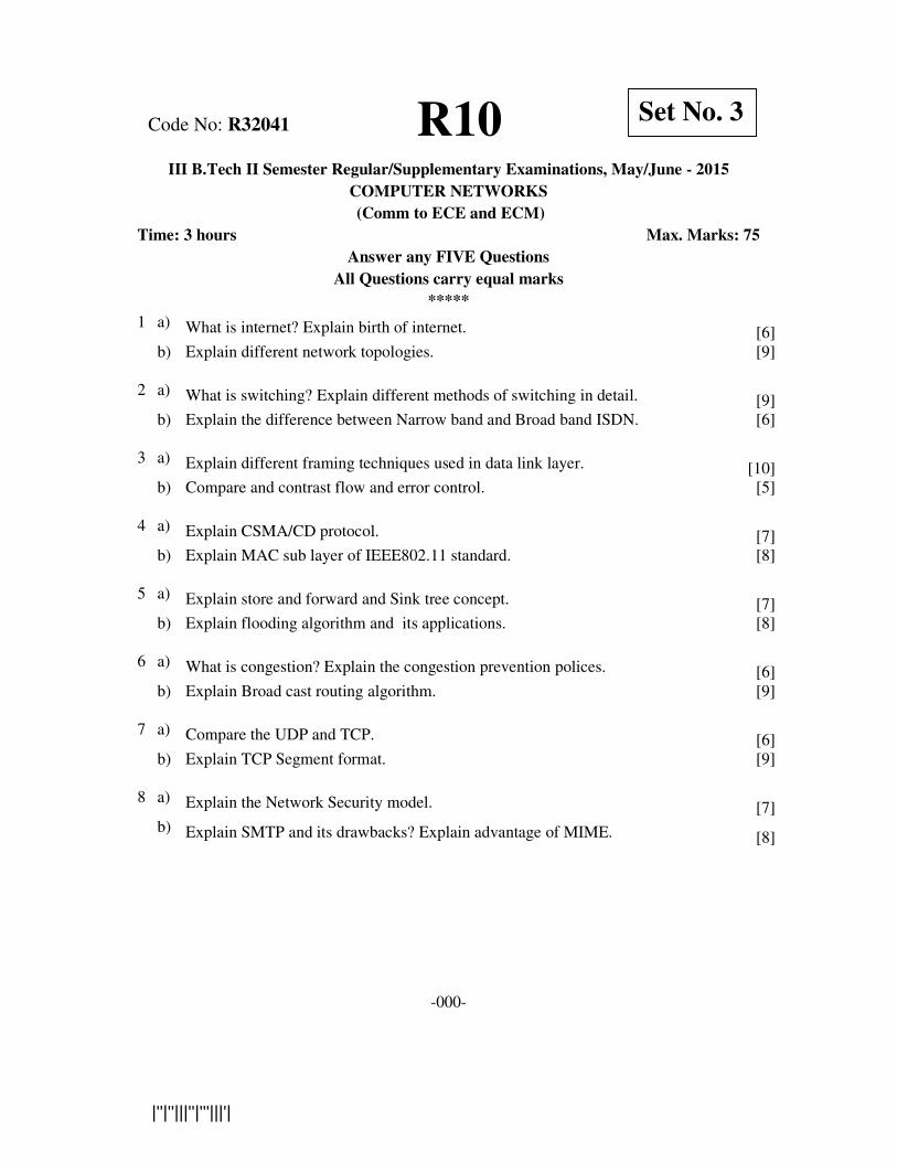
4 A project consists of nine activities and three time estimates. Find
a) Expected time variance
b) Network diagram
c) Calculate Earliest times, Latest times and floats
d) Critical path and duration
Activity Optimistic Time Most likely Time Pessimistic Time
1-2 3 6 15
1-6 2 5 14
2-3 6 12 30
2-4 2 5 8
3-5 5 11 17
4-5 3 6 15
6-7 3 9 27
5-8 1 4 7
7-8 4 19 28
[15]
5 a) What are the factors of external and internal environmental to be considered for
Formulating the strategy? Explain.
[8]
b) Describe the process of strategic management.
[7]
6 a) Write about the importance of ethics in marketing? [7]
b) What are the basic principles of business ethics?
1 of 2
[8]
Code No: R32026 Set No. 2 R10

|''|''|||''|'''|||'|
7 a) Briefly explain the various techniques of business communication. [8]
b) Explain the problems and challenges of cross cultural communication.
[7]
8 a) What is Enterprise Resource Planning? Explain. [7]
b) Explain the merits and demerits of Enterprise Resource Planning.
*****
[8]
2 of 2
Code No: R32026 Set No. 2 R10

|''|''|||''|'''|||'|
III B.Tech II Semester Regular/ Supplementary Examinations, May/June - 2015
MANAGEMENT SCIENCE (Common to EEE, ECE, CSE, CHEM, EIE, BME, IT)
Time: 3 hours Max. Marks: 75
Answer any FIVE Questions
All Questions carry equal marks
*****
1 a) Describe the theory of scientific management and explain how it was criticized. [8]
b) What is matrix organization and what is its uniqueness?
[7]
2 a) What do you mean by EOQ? Derive the formula for determining the EOQ. [8]
b) Define Control charts and explain its types.
[7]
3 a) What do you understand by marketing mix? [8]
b) Explain briefly the basic elements in marketing mix.
[7]
4 A small project is composed of the following activities whose time estimates are
given below.
Activity Predecessor Optimistic Time Most likely Time Pessimistic Time
A - 2 4 6
B A 8 12 16
C A 14 16 30
D B 4 10 16
E C, B 6 12 18
F E 6 8 22
G D 18 18 30
H F, G 8 14 32
i) Draw the network and find the critical path.
ii) Compute the expected project completion time.
iii) Calculate Earliest times and Latest times
[15]
5 a) Define strategic management and describe the process of strategic management. [8]
b) How do you carry out SWOT analysis for a manufacturing unit?
[7]
6 a) What is Ethics? Explain the importance of ethics in HRM. [8]
b) Write about the importance of ethics in marketing.
1 of 2
[7]
Code No: R32026 Set No. 3 R10

|''|''|||''|'''|||'|
7 a) Explain the various elements of writing a good report. [8]
b) What are the skills required to effective presentation?
[7]
8 Write a notes on : a) Supply Chain Management
b) Performance Management.
*******
[8]
[7]
2 of 2
Code No: R32026 Set No. 3 R10
|''|''|||''|'''|||'|
III B.Tech II Semester Regular/ Supplementary Examinations, May/June - 2015
MANAGEMENT SCIENCE (Common to EEE, ECE, CSE, CHEM, EIE, BME, IT)
Time: 3 hours Max. Marks: 75
Answer any FIVE Questions
All Questions carry equal marks
*****
1 a) Why is management considered as a profession and what factors make it a
profession?
[8]
b) Distinguish between Theory – X and Theory – Y.
[7]
2 a) What is meant by materials management? State its advantages and disadvantages. [8]
b) Explain the types of ABC analysis.
[7]
3 a) State the importance and methods of job evaluation. [8]
b) Define training and explain its methods.
[7]
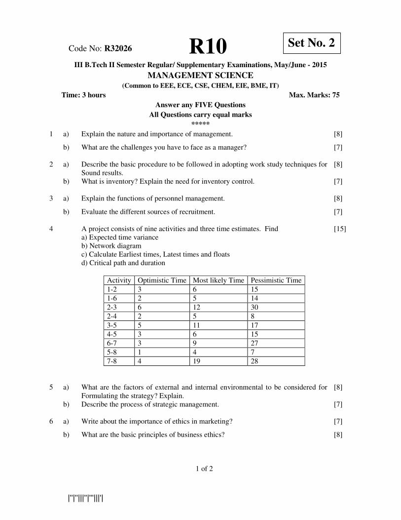
4 A PERT network has the following activities with their time estimates given
below. You are required to calculate the expected time of activities, draw the
network and find the critical path and its duration.
Activity Optimistic Time Most likely Time Pessimistic Time
0-1 2 3.5 8
0-2 3 3.75 6
0-3 1 2.5 7
1-2 3 7.5 9
1-4 4 5.5 10
2-4 2 5 8
3-4 2 2.75 5
3-5 3 6 9
4-5 2 5 8
[15]
5 a) What do you understand by the concept of strategy? Discuss the concept of
Mission And Vision.
[8]
b) Explain strategy variations and Generic strategy alternatives.
[7]
6 a) Discuss about the basic principles of business ethics. [8]
b) Explain the importance of Ethics in business management?
[7]
7 a) Explain various methods of interviews in detail. [8]
b) What is conference and briefly explain the video conferences.
[7]
8 Write a notes on: a) Capability Maturity Model
b) Balanced Score card
[8]
[7]
****
Code No: R32026 Set No. 4 R10

|''|''|||''|'''|||'|
III B.Tech II Semester Regular/Supplementary Examinations, May/June - 2015
MICROPROCESSORS AND MICROCONTROLLERS
(Com to ECE, ECM, BMI, EIE)
Time: 3 hours Max. Marks: 75
Answer any FIVE Questions
All Questions carry equal marks
*****
1 a) Draw the minimum mode Read operation timing diagram and its operation in detail. [8]
b) Explain the purpose of Flag register and how many conditional and control flags
presented in 8086 Microprocessor.
[7]
2 a) Write an assemble language program to arrange the given array in ascending order,
the length of array is ten 16-bit numbers.
[8]
b) Draw the interrupt cycle of 8086 Microprocessor and explain the nested interrupt
concept in detail.
[7]
3 a) a) Interfacing of Two 8X8 RAM and Two 16X8 EPROM with 8086 CPU, the
EPROM starting address is 00000H. The RAM address follows the EPROM. Draw
the memory interfacing table along with interfacing diagram.
[10]
b) List out the difference between Static RAM and EPROM in detail.
[5]
4 a) Draw the internal architecture of 8257 DMA and explain the operation of each block. [8]
b) Draw the mode set and status register of 8257 DMA and explain the operation of
each field.
[7]
5 a) Draw the flag register of 80386 processor and Explain the register organization of
this processor.
[8]
b) Briefly explain the salient futures in an 80386 processor and compare them with an
80286 processor.
[7]
6 a) Explain the different addressing modes of 8051 Microcontroller along with
examples.
[10]
b) Briefly explain the difference between Microprocessor and microcontroller in detail.
[5]
7 a) Draw the pin diagram of PIC 16C61 controller and explain the function of each pin
in detail.
[8]
b) Explain the different interrupts presented in PIC 16C61 controller in detail.
[7]
8 Write short notes on following
a) Thumb instruction set of ARM controller
b) Register organization of ARM controller.
[8+7]
*****
Code No: R32044 Set No. 1 R10

|''|''|||''|'''|||'|
III B.Tech II Semester Regular/Supplementary Examinations, May/June - 2015
MICROPROCESSORS AND MICROCONTROLLERS
(Com to ECE, ECM, BMI, EIE)
Time: 3 hours Max. Marks: 75
Answer any FIVE Questions
All Questions carry equal marks
*****
1 a) Explain the following 8086 Microprocessor pins in detail.
(i)RQ0/GT0 (ii) BHE (iii) HOLD, HLDA (iv) QS0, QS1
[8]
b) Explain the machine language instruction formats of 8086 Microprocessor in detail.
[7]
2 a) Explain the shift and Rotate instruction set of 8086 Microprocessor along with
examples.
[8]
b) List out the different mask able and non-mask able interrupt of 8086
Microprocessor and explain its importance.
[7]
3 a) Draw the 8255 PPI internal block diagram and explain its operation in detail. [8]
b) Draw the format of BSR mode and I/O mode and explain each bit in detail.
[7]
4 a) Explain the different methods used in serial communications in detail. [8]
b) Draw the internal architecture of 8251 USART and explain the operation of each
block.
[7]
5 a) Explain the concept of Real and protected modes of an 80386 processor along with
circuit diagram.
[8]
b) Explain the different instruction set of an 80386 processor along with examples.
[7]
6 Explain the following special function registers of 8051 microcontroller
(i) SCON (ii) TMOD (iii)PSW (iv) TCON
[15]
7 a) Draw the internal architecture of PIC 16C61 controller and explain its operation. [8]
b) Explain the differing between PIC 16C61 and PIC 16C71 controller in detail.
[7]
8 a) Draw the format of program status register of ARM controller and explain the
function of each bit in detail.
[8]
b) Explain the different ARM Instruction set of ARM processor and explain each
instruction with example.
[7]
*****
Code No: R32044 Set No. 2 R10

|''|''|||''|'''|||'|
III B.Tech II Semester Regular/Supplementary Examinations, May/June - 2015
MICROPROCESSORS AND MICROCONTROLLERS
(Com to ECE, ECM, BMI, EIE)
Time: 3 hours Max. Marks: 75
Answer any FIVE Questions
All Questions carry equal marks
*****
1 a) Draw the Register organization of 8086 Microprocessor and explain the operation
of each register in detail.
[8]
b) Define addressing mode and explain the different addressing modes presented in
8086 Microprocessor with examples.
[7]
2 a) Define Interrupt and explain the interrupt services routines in 8086
Microprocessor.
[8]
b) Write an assemble language program to find the sum of the squares of first ten
numbers.
[7]
3 a) Explain Stepper motor interfacing along with interfacing diagram. [10]
b) Briefly list out the importance features of Static RAM interfacing and Dynamic
RAM interfacing.
[5]
4 a) Draw the internal architecture of 8579 keyboard and display controller and explain
the operation of each block.
[8]
b) Draw and Explain the frame format of ICW’s and OCW’s concept of 8259
Programmable interrupt controller.
[7]
5 a) Define paging. Draw and explain the paging mechanism of 80386 processor. [5]
b) Draw the pin diagram of an80386 processor and explain the function of each pin in
detail.
[10]
6 a) Draw the pin diagram of 8051 Microcontroller and explain the function of each
port in detail.
[8]
b) Draw the Internal RAM memory organization of 8051 Microcontroller and explain
its operation.
[7]
7 Explain the future of PIC 16F8XX flash controller, Draw its status resisters and
compare them in to PIC 16C61 controller in detail.
[15]
8 Write short notes on following.
(i) Thumb programming model in ARM controller
(ii) ARM Development tools
[8+7]
*****
Code No: R32044 Set No. 3 R10
|''|''|||''|'''|||'|
III B.Tech II Semester Regular/Supplementary Examinations, May/June - 2015
MICROPROCESSORS AND MICROCONTROLLERS
(Com to ECE, ECM, BMI, EIE)
Time: 3 hours Max. Marks: 75
Answer any FIVE Questions
All Questions carry equal marks
*****
1 a) Define assembler directive and explain different assembler directives used in 8086
Microprocessor in detail.
[8]
b) Explain the concept of Physical memory organization of 8086 Microprocessor with
example.
[7]
2 a) Draw the stack structure of 8086 Microprocessor and explain its need while
presenting an interrupt.
[8]
b) Write an assemble language program for finding the Largest number in an Array,
the length of array is ten 16-bit numbers.
[7]
3 a) Draw the functional diagram, pin diagram of ADC0808, and explain its operation
along with interfacing diagram.
[10]
b) Write short notes on control of high power devices using 8255 programmable
peripherals input output port.
[5]
4 a) Draw the Internal architecture of 8259 Programmable interrupt controller and
explain the operation of each block in detail.
[8]
b) Explain the different operating modes of 8259 Programmable interrupt controller in
detail.
[7]
5 a) Explain different data types and addressing modes used in 80386 processor with
examples.
[10]
b) Briefly explain the features of an 80486 processor and also compare with an 80386
processor.
[5]
6 a) Draw the internal architecture of 8051 Microcontroller and explain the operation of
each block.
[8]
b) Explain the different assembly programming tools used in 8051 microcontroller in
detail.
[7]
7 a) Explain the different ports presented in PICF8XX Flash controller and also give the
alternate function of each port.
[8]
b) Draw the frame format of different timers presented in PIC 16F8XX flash controller
and explains function of each bit.
[7]
8 a) Draw the data flow diagram of ARM architecture and explain the function of each
block in it along with different future in it.
[10]
b) Explain the different development tools used in ARM Microcontroller in detail. [5]
*****
Code No: R32044 Set No. 4 R10

|''|''|||''|'''|||'|
III B.Tech II Semester Regular/Supplementary Examinations, May/June - 2015
MICROWAVE ENGINEERING
(Electronics and Communication Engineering)
Time: 3 hours Max. Marks: 75
Answer any FIVE Questions
All Questions carry equal marks
*****
1 a) What are microwaves? Explain the applications of microwaves. [7]
b) Derive expressions for cutoff wavelength and cutoff frequency for TM waves
propagating through rectangular waveguides.
[8]
2 a) Sketch circular and rectangular waveguides and give the comparison. [7]
b) Explain the impossibility of TEM wave propagating through the waveguide.
[8]
3 a) What is the effect of discontinuity in a waveguide? Discuss in detail. [7]
b) How many types of waveguide phase shifters are there? Discuss one type in
detail.
[8]
4 a) Explain the operation of magic tee with its s-parameter. List the applications of
magic tee.
[9]
b) A 3-port circulator has an insertion loss of 1 dB, isolation 30 dB and VSWR
is 1. Find the S-matrix.
[6]
5 a) With neat circuit diagram, explain the velocity modulation process with
applegate diagram in Klystron amplifier.
[9]
b) Explain the limitations of conventional tubes at UHF and at microwave.
[6]
6 a) Explain about crossed field device and also describe why strapping is needed. [7]
b) Explain the mechanism of oscillations of Magnetron oscillator with the aid of
suitable diagram and discuss its performance characteristics.
[8]
7 a) What is transferred electron effect? Explain about any one of transferred
electron devices.
[8]
b) Explain about Gunn effect using two valley theory.
[7]
8 a) Describe how the power of microwave generator can be measured using
Bolometer method. [8]
b) Explain the measurement of Low and High VSWR. [7]
-000-
Code No: R32042 Set No. 1 R10

|''|''|||''|'''|||'|
III B.Tech II Semester Regular/Supplementary Examinations, May/June - 2015 MICROWAVE ENGINEERING
(Electronics and Communication Engineering)
Time: 3 hours Max. Marks: 75
Answer any FIVE Questions
All Questions carry equal marks
*****
1 a) Why does the TEM mode cannot propagate through hollow rectangular
waveguide? Derive wave equations for rectangular wave guide
[9]
b) Define the following terms with respect to waveguide:
(i) Phase velocity (ii) Group velocity
[6]
2 a) Explain the mathematical analysis of rectangular waveguide. [6]
b) Explain TE, TM and TEM modes in a waveguide. What is meant by the
dominant mode in a rectangular waveguide? Explain.
[9]
3 a) What are the advantages of S parameters over Z and Y parameters? [7]
b) A 10 mW signal is applied to a 20 dB directional coupler. Determine the power
available at the coupled port.
[8]
4 a) With a neat sketch explain the operation of Magic Tee and derive its S matrix. [9]
b) State and explain the properties of S parameters.
[6]
5 a) Describe the construction and working of a reflex klystron. Explain how
velocity and current modulation takes place using the applegate diagram.
[9]
b) What is meant by applegate diagram? Explain about bunching in two cavity
klystron.
[6]
6 a) Explain the mechanism of oscillations in Magnetron oscillator with the aid of
suitable diagram and discuss its performance characteristics.
[8]
b) Explain the amplification process for a helix type travelling wave tube. List its
applications.
[7]
7 a) Discuss the merits and demerits of IMPATT diode.
[7]
b)
Explain the Gunn diode with its Gunn oscillation modes.
[8]
8 Briefly explain about different blocks of Microwave bench and their features.
[15]
-000-
Code No: R32042 Set No. 2 R10

|''|''|||''|'''|||'|
III B.Tech II Semester Regular/Supplementary Examinations, May/June - 2015
MICROWAVE ENGINEERING
(Electronics and Communication Engineering)
Time: 3 hours Max. Marks: 75
Answer any FIVE Questions
All Questions carry equal marks
*****
1 a) A rectangular waveguide ( a=2 cm, b=1 cm) filled with de-ionized water ( µ r =
1, εr = 81 ) operates at 3 GHz. Determine all propagating modes and the
corresponding cutoff frequencies.
[9]
b) Define the following terms with respect to waveguide:
(i) Wavelength (ii) Impedance relations
[6]
2 a) Discuss the advantages and disadvantages of microstrip lines. [8]
b) A circular waveguide operating in the dominant mode at a frequency of 9GHz
with maximum field strength of 300 V/cm. The internal diameter is 5cm.
Calculate the maximum power.
[7]
3 a) With a neat sketch explain the construction and operation of H-plane Tee
junction.
[8]
b) Discuss in detail about single hole and double hole directional coupler.
[7]
4 a) Explain the action of isolator, gyrator and circulator using ferrites. Mention
their typical applications.
[8]
b) Show that the sum of the terms of any column of the S matrix of a lossless
network when multiplied by the complex conjugate of the corresponding terms
of any other column is zero.
[7]
5 a) Give the difference between two cavity klystron and reflex klystron. Also draw
the schematic of reflex klystron and explain its working.
[10]
b) Differentiate between klystron and travelling wave tubes.
[5]
6 a) Draw different slow wave structures and explain why slow wave structures are
used in travelling wave tubes.
[8]
b) Draw cavity magnetron and explain its working for π-mode.
[7]
7 a) Discuss the formation of high field domain in TEDs. [7]
b) Explain the LSA mode of operation in a Gunn diode.
[8]
8 a) How are microwave measurements different from low frequency
measurements?
[6]
b) Briefly explain the classification of power measurements.
[9]
-000-
Code No: R32042 Set No. 3 R10
|''|''|||''|'''|||'|
III B.Tech II Semester Regular/Supplementary Examinations, May/June - 2015 MICROWAVE ENGINEERING
(Electronics and Communication Engineering)
Time: 3 hours Max. Marks: 75
Answer any FIVE Questions
All Questions carry equal marks
*****
1 a) Derive expressions for guide wavelength, phase velocity and group velocity for TM
waves in circular waveguide.
[9]
b) Find the first five resonances of an air-filled rectangular cavity with dimensions of a=5
cm, b=4 cm and c=10 cm (c>a>b).
[6]
2 a) Calculate the resonant frequency of a circular resonator of following dimensions.
Diameter = 12.5cm and length = 5cm for TM012 mode (consider Pmn=2.405 for dominant
mode).
[6]
b) What are cavity resonators? Derive the equations for resonant frequencies for
rectangular and circular cavity resonators.
[9]
3 a) A directional coupler has a coupling factor of 15 dB. An input signal of 5W is applied.
Determine the directivity of the directional coupler if the power measured at the isolated
port is 10 mW.
[7]
b) Define coupling factor, directivity and isolation of directional coupler and write
expression for each.
[8]
4 a) In an H-plane Tee junction, 20mW power is applied to port 3 that is perfectly matched
to the junction. Calculate the power delivered to the load 60Ω and 75Ω connected to
ports 1 and 2.
[8]
b) Derive the S-Matrix for 3-port isolator.
[7]
5 a) Explain the classification of microwave tubes. [9]
b) A reflex klystron is operating at 100 GHz. If the mode operating in the tube corresponds
to n=4, determine the transit time of the electron in the repeller space.
[6]
6 a) Write a brief note on the following:
(i) π mode operation of magnetron (ii) slow wave structures [9]
b) Discuss the performance of magnetrons and list the important applications.
[6]
7 a) An IMPATT diode has a Cj of 0.05pF and Lp of 0.5nH, Cp is negligible. If the
breakdown voltage is 100V and the bias current is 100mA. Determine the resonant
frequency and efficiency. Assume the RF peak current as 0.8A and RL as 2Ω
[8]
b) Discuss the differences between transferred electron devices and avalanche transit time
devices.
[7]
8 a) Give the block diagram for the measurement of impedance at microwave frequencies
and explain the procedure. [9]
b) Calculate the SWR of a transmission system operating at 8GHz. The distance between
two minimum power points is 0.9mm on a slotted line whose velocity factor is unity. [6]
-000-
Code No: R32042 Set No. 4 R10

|''|''|||''|'''|||'|
III B.Tech II Semester Regular/Supplementary Examinations, May/June - 2015
VLSI DESIGN
(Comm to ECE, ECM, EIE)
Time: 3 hours Max. Marks: 75
Answer any FIVE Questions
All Questions carry equal marks
*****
1 a) With a neat sketch explain BICMOS fabrication in p-well process and also explain its
operation. [8]
b) What are the advantages of SOI?
[7]
2 a) Explain effect of threshold voltage on MOSFET current equations. [8]
b) For a CMOS inverter calculates the shift in transfer characteristic curve when βn/βp ratio is
varied from 1/1 to 10/1.
[7]
3 a) What is a stick diagram and explain different symbols used for components in stick diagram. [8]
b) Design a layout diagram for pMOS logic Y= (AB+CD)/
[7]
4 a) What is inverter delay? How delay is calculated for multiple stages. [7]
b) Two nMOS inverters are cascaded to drive a capacitive load CL = 16 Cg. Calculate the pair
delay in turns of τ for the inverter indicated in the figure below. What are the ratios of each
inverter?
Inverter 1 Inverter 2
LPU = 16 λ LPU = 2 λ
WPU = 2 λ WPU = 2 λ
LPd = 2 λ LPd = 2 λ
WPd = 2 λ WPd = 8 λ
[8]
5 a) Explain clocked CMOS logic, domino logic and n-PCMOS logic. [8]
b) Explain switch logic and its arrangements? [7]
6 a) Draw the typical standard cell structure showing regular-power cell and explain it. [8]
b) Explain the principle of gate arrays. [7]
7 a) What are procedures? How are they used in VHDL? Explain. [8]
b) Give the comparisons of Concurrent and Sequential Statements. [7]
8 a) With the help of a block diagram, explain the stages of compilation, elaboration and
simulation. [8]
b) Describe synthesis of VHDL code with examples. [7]
*****
Code No: R32045 Set No. 1 R10

|''|''|||''|'''|||'|
III B.Tech II Semester Regular/Supplementary Examinations, May/June - 2015
VLSI DESIGN
(Comm to ECE, ECM, EIE)
Time: 3 hours Max. Marks: 75
Answer any FIVE Questions
All Questions carry equal marks
*****
1 a) Explain the nMOS enhancement mode fabrication process for different conditions of
Vds?
[8]
b) Explain latch up problems in CMOS circuits?
[7]
2 a) Explain different forms of pull ups used as load in CMOS and in enhancement and
depletion modes of nMOS.
[8]
b) An nMOS transistor is operating in active region with the following parameters:
VGS=3.9V,Vtn=1V,W/L=100,µnCox=90µA/V2. Find ID and RDS.
[7]
3 a) What is the need for design rules? Explain different types of design rules. [8]
b) Draw the stick diagram layout for y= (A.B) +E+ (C.D)
[7]
4 a) What is sheet resistance? Derive the Expression for RS? [7]
b) Calculate the ON resistance from VDD to GND for the nMOS and CMOS inverter
circuits.
[8]
5 a) Explain about static, dynamic and domino logics with examples. [8]
b) What are the limitations on scaling in VLSI design?
[7]
6 a) Draw the typical architecture of PLA and explain its operation. [8]
b) What are the advantages, disadvantages and applications of PLAs?
[7]
7 a) Explain package declaration and package body in VHDL with an example. [8]
b) Bring out the comparisons between VHDL functions and procedures.
[7]
8 a) Explain the different styles of modeling in VHDL. Discuss the salient features of them
taking the example of a full adder.
[8]
b) Write a short note on Technology Libraries? [7]
*****
Code No: R32045 Set No. 2 R10

|''|''|||''|'''|||'|
III B.Tech II Semester Regular/Supplementary Examinations, May/June - 2015
VLSI DESIGN
(Comm to ECE, ECM, EIE)
Time: 3 hours Max. Marks: 75
Answer any FIVE Questions
All Questions carry equal marks
*****
1 a) Elaborate steps in pMOS fabrication process with suitable sketch? [8]
b) Give the steps for single metal CMOS n-well process and additional steps for bipolar
devices.
[7]
2 a) Clearly explain channel length modulation of the MOSFET. [7]
b) Define threshold voltages of a MOS device and explain its significance.
[8]
3 a) Explain 2µm Double Metal, Double Poly. CMOS / BiCMOS Rules. [8]
b) Design stick diagram for nMOS logic Y= ((A+B).C)/
[7]
4 a) Explain different interconnect parasitics. [7]
b) Explain the problem of driving large capacitive loads? How such loads can be
driven?
[8]
5 Discuss the limits of scaling. Why scaling is necessary for VLSI circuits?
[15]
6 a) With neat schematic explain the architectural building blocks of CPLD? [7]
b) Explain the following terms:
i) LUT ii) CLB iii) IOB iv) Switch matrix
[8]
7 a) Discuss the various data types in VHDL with examples. [8]
b) Explain the following with declaration format and an example each:
i) Variable ii) Signal iii) Constant
[7]
8 a) List the three styles of modeling a digital system in VHDL. Give the VHDL code for
each of them, with reference to half adder.
[8]
b) Explain about synthesis process? [7]
*****
Code No: R32045 Set No. 3 R10

|''|''|||''|'''|||'|
III B.Tech II Semester Regular/Supplementary Examinations, May/June - 2015
VLSI DESIGN
(Comm to ECE, ECM, EIE)
Time: 3 hours Max. Marks: 75
Answer any FIVE Questions
All Questions carry equal marks
*****
1 a) Explain the steps in twin-tub process of CMOS fabrication with suitable sketch. [8]
b) What are the advantages of BICMOS process over CMOS technology?
[7]
2 a) Derive an equation for transconductance of an n-channel enhancement MOSFET
operating in active region.
[8]
b) Explain the possibility of using a CMOS inverter as an amplifier.
[7]
3 a) Explain 2µm CMOS design rules for wires. [8]
b) Design a stick diagram for CMOS logic Y= (A+B+C)/.
[7]
4 a) Explain the model for deviation of time delay. [7]
b) Two nMOS inverters are cascaded to drive a capacitive load CL=16Cg. Calculate pair
delay Vin to Vout in terms of τ.
[8]
5 a) Draw the basic structure of a dynamic CMOS gate and explain. [8]
b) How switch logic can be implemented using Pass Transistors?
[7]
6 a) What are FPGAs? Explain the principle and operation. [8]
b) Explain how the pass transistors are used to connect wire segments for the purpose of
FPGA programming.
[7]
7 Write short notes on
a) File types b) Drivers c) Statement concurrency d) Attributes
[15]
8 a) Explain in brief the evolution of VHDL and mention the capabilities of the language. [8]
b) Explain about simulation process in VHDL. [7]
*****
Code No: R32045 Set No. 4 R10
![Micro Processors & Micro Controllers Lecture Notesgopalmic.weebly.com/uploads/6/0/3/4/6034310/mpi_full_document.pdfMicro Processors & Micro Controllers Lecture Notes (As Per JNTUK-[R07]](https://img.dokumen.tips/doc/110x75/5aa2476a7f8b9a1f6d8d063d/micro-processors-micro-controllers-lecture-processors-micro-controllers-lecture.jpg)