Embed Size (px)
Citation preview
Computer ArchitectureChapter 5
Fall 2005
Department of Computer Science
Kent State University
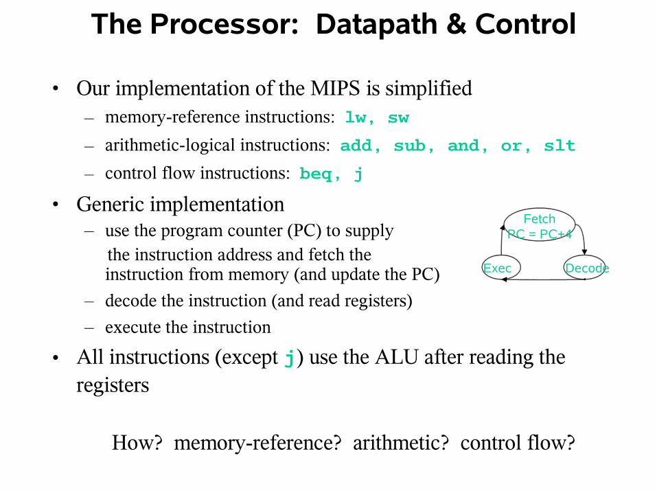
• Our implementation of the MIPS is simplified– memory-reference instructions: lw, sw
– arithmetic-logical instructions: add, sub, and, or, slt
– control flow instructions: beq, j
• Generic implementation– use the program counter (PC) to supply the instruction address and fetch the
instruction from memory (and update the PC)
– decode the instruction (and read registers)
– execute the instruction
• All instructions (except j) use the ALU after reading the registers
How? memory-reference? arithmetic? control flow?
The Processor: Datapath & Control
FetchPC = PC+4
DecodeExec

• Two types of functional units:– elements that operate on data values (combinational)
– elements that contain state (sequential)
Abstract / Simplified View
Data
Register #
Register #
Register #
PC Address Instruction
Instructionmemory
Registers ALU Address
Data
Datamemory
AddAdd
4

More Implementation Details
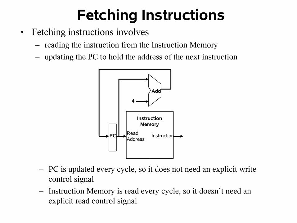
Fetching Instructions• Fetching instructions involves
– reading the instruction from the Instruction Memory
– updating the PC to hold the address of the next instruction
ReadAddress
Instruction
InstructionMemory
Add
PC
4
– PC is updated every cycle, so it does not need an explicit write control signal
– Instruction Memory is read every cycle, so it doesn’t need an explicit read control signal
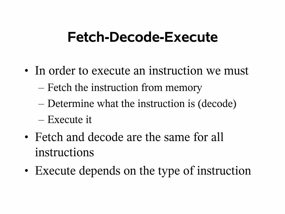
Fetch-Decode-Execute
• In order to execute an instruction we must– Fetch the instruction from memory
– Determine what the instruction is (decode)
– Execute it
• Fetch and decode are the same for all instructions
• Execute depends on the type of instruction

Instruction Formats
5:010:615:1120:1625:2131:26
functshamtrdrtrsop
15:020:1625:2131:26
immedrtrsop
25:031:26
addrop
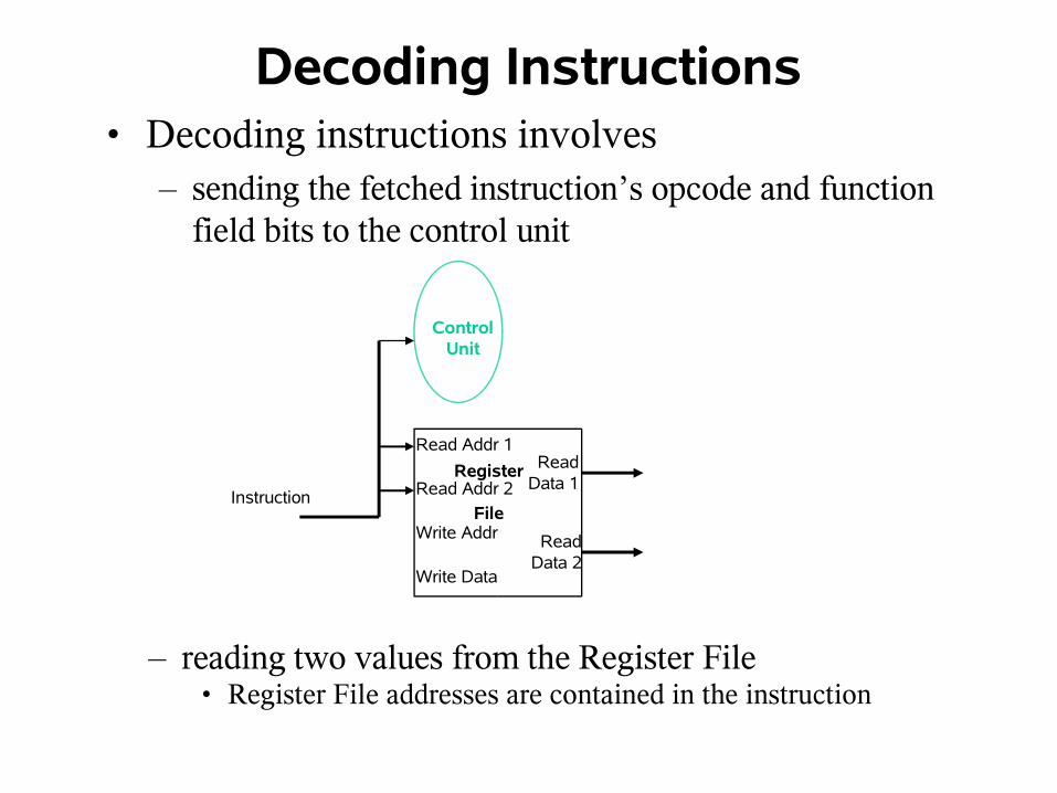
Decoding Instructions• Decoding instructions involves
– sending the fetched instruction’s opcode and function field bits to the control unit
Instruction
Write Data
Read Addr 1
Read Addr 2
Write Addr
Register
File
Read Data 1
Read Data 2
ControlUnit
– reading two values from the Register File• Register File addresses are contained in the instruction
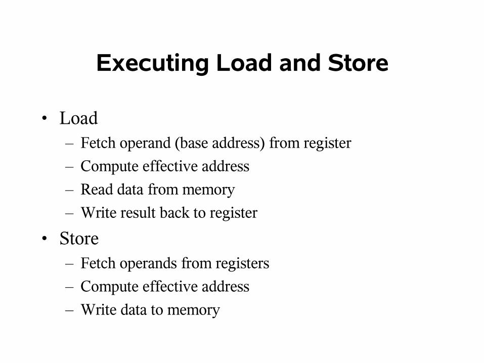
Executing Load and Store
• Load– Fetch operand (base address) from register
– Compute effective address
– Read data from memory
– Write result back to register
• Store– Fetch operands from registers
– Compute effective address
– Write data to memory

Executing Arithmetic/Logic
• Arithmetic/logic (add, sub, and, or, slt)– Fetch operands from registers
– Perform operation
– Write result back to register

Executing Branch and Jump
• Conditional branch (beq)– Fetch operands from registers
– Compare operands
– If equal add displacement to PC
• Jump (j)– Write new value to PC

ALU Instructions
• Components– Register File
– ALU
• Operation– Use instruction fields to select registers
– Read source registers and send them to ALU
– Send ALU result to destination register

Components for ALU Instrs
ALU control
RegWrite
RegistersWrite register
Read data 1
Read data 2
Read register 1
Read register 2
Write data
ALU result
ALU
Data
Data
Register numbers
a. Registers b. ALU
Zero5
5
5 3

ALU Datapath
InstructionRegisters
Write register
Read data 1
Read data 2
Read register 1
Read register 2
Write data
ALU result
ALU
Zero
RegWrite
ALU operation3

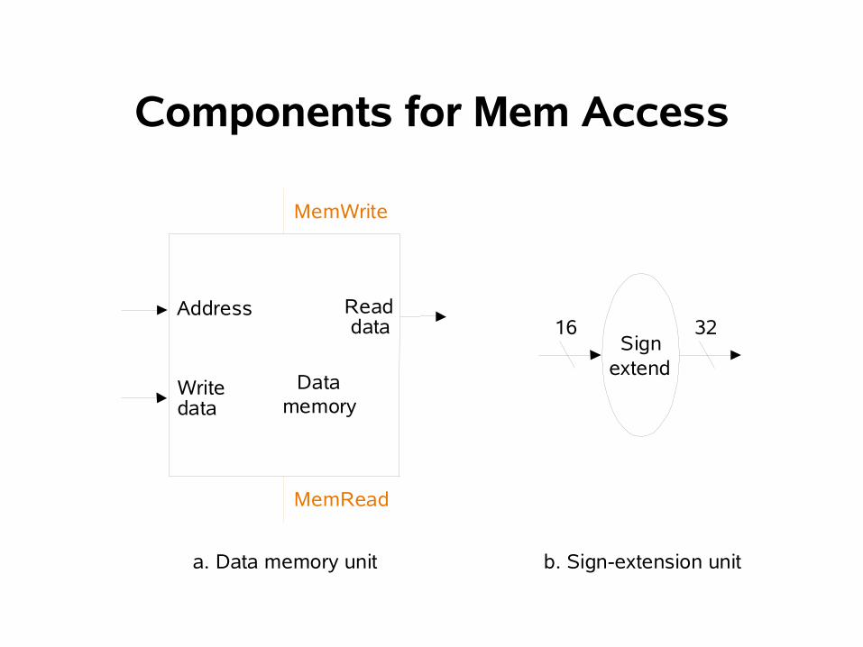
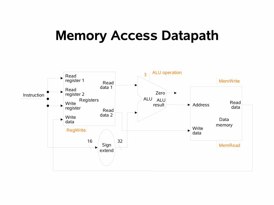
Memory Access
• Components– Register File– ALU– Data Memory– Sign-Extension Unit
• Operation– ALU adds base register and sign-extended immediate– Send ALU result to memory as the address– Read the value from memory into the destination register
(lw) or write the value from the source register into memory (sw)
Components for Mem Access
16 32Sign
extend
b. Sign-extension unit
MemRead
MemWrite
Data memory
Write data
Read data
a. Data memory unit
Address
Memory Access Datapath
Instruction
16 32
RegistersWrite register
Read data 1
Read data 2
Read register 1
Read register 2
Data memory
Write data
Read data
Write data
Sign extend
ALU result
ZeroALU
Address
MemRead
MemWrite
RegWrite
ALU operation3

Branches
• Components– Register File– ALU– Program Counter (PC)– Adder– Sign-Extension Unit
• Operation– Send source register values to ALU for comparison– Adder computes branch target address– Control logic decides whether branch is taken or not

Branch Datapath
16 32Sign
extend
ZeroALU
Sum
Shift left 2
To branch control logic
Branch target
PC + 4 from instruction datapath
Instruction
Add
RegistersWrite register
Read data 1
Read data 2
Read register 1
Read register 2
Write data
RegWrite
ALU operation3

Putting It All Together
MemtoReg
MemRead
MemWrite
ALUOp
ALUSrc
RegDst
PC
Instruction memory
Read address
Instruction [31– 0]
Instruction [20– 16]
Instruction [25– 21]
Add
Instruction [5– 0]
RegWrite
4
16 32Instruction [15– 0]
0Registers
Write registerWrite data
Write data
Read data 1
Read data 2
Read register 1Read register 2
Sign extend
ALU result
Zero
Data memory
Address Read data M
u x
1
0
M u x
1
0
M u x
1
0
M u x
1
Instruction [15– 11]
ALU control
Shift left 2
PCSrc
ALU
Add ALU result

Control Unit
• Control unit takes an instruction as input and produces control signals as output
• Types of control signals– Multiplexor selector signals– Write enables for state elements– Control signals for other blocks (ALU, etc.)
• In a single-cycle datapath the control unit is simple, just look up instruction in a table
Control Signals
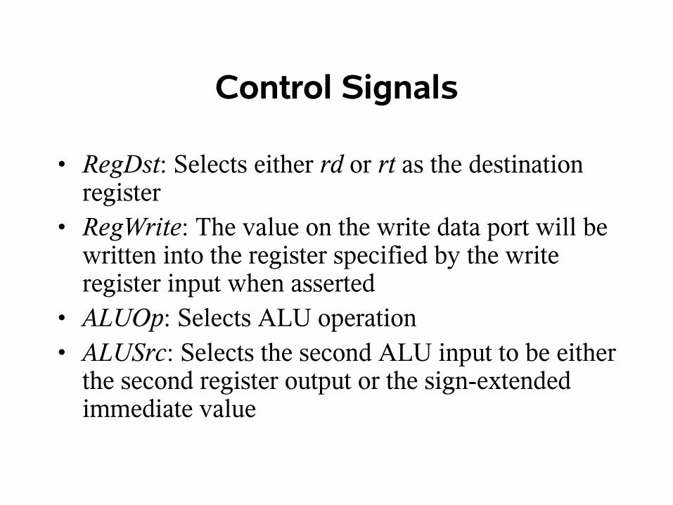
• RegDst: Selects either rd or rt as the destination register
• RegWrite: The value on the write data port will be written into the register specified by the write register input when asserted
• ALUOp: Selects ALU operation• ALUSrc: Selects the second ALU input to be either
the second register output or the sign-extended immediate value

Control Signals (cont'd)
• PCSrc: Selects new PC as either PC + 4 or the output of the branch target adder– This signal is derived from the Branch control signal and
the ALU's Zero output
• MemRead/MemWrite: Causes data memory to perform a read/write operation when asserted
• MemToReg: Selects either the ALU output or the data memory output as the data input into the register file

ALU Control
• In order to simplify design of the control unit we give the ALU its own control logic
• The ALU control block takes a 2-bit input from the control unit (ALUOp) and the funct field from the instruction and produces the ALU control signals

ALU Control Signals
0111Set on less than10101010slt
0001OR10010110or
0000AND10010010and
0110Subtract10001010sub
0010Add10000010add
0110Subtract01beq
0010Add00sw
0010Add00lw
ALU InputsALU Functionfunct FieldALUOpInstruction
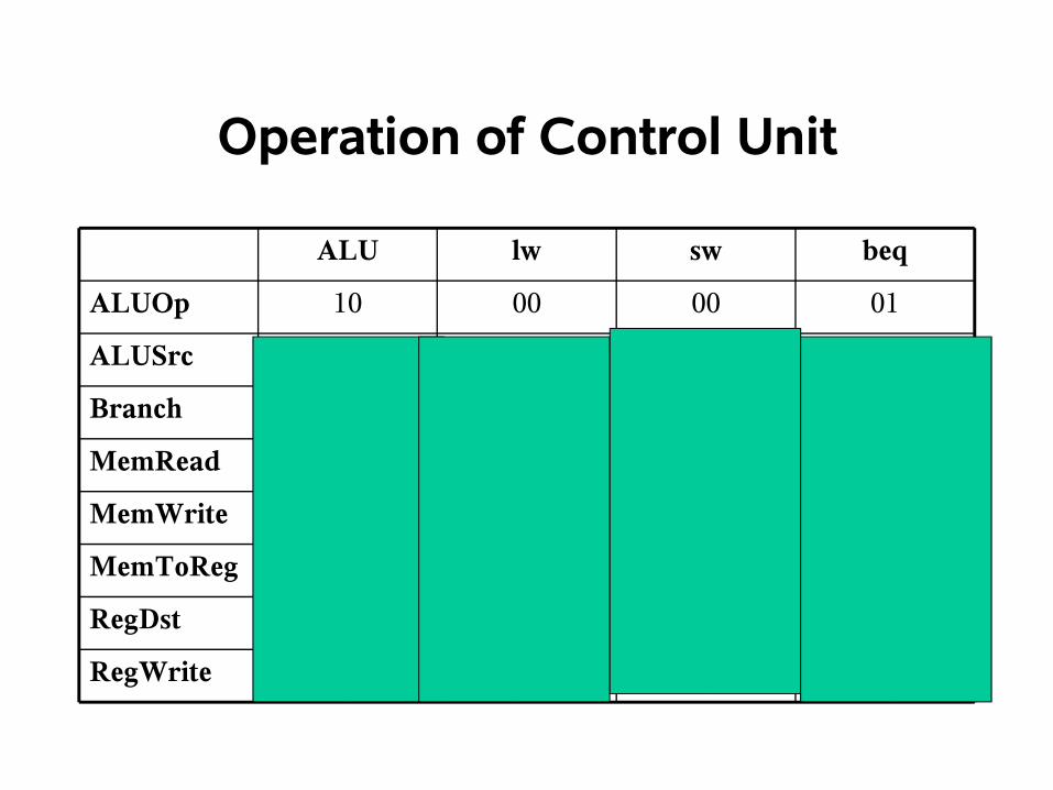
Operation of Control Unit
0011RegWrite
xx01RegDst
xx10MemToReg
0100MemWrite
0010MemRead
1000Branch
0110ALUSrc
01000010ALUOp
beqswlwALU

Datapath with Control Unit
PC
Instruction memory
Read address
Instruction [31– 0]
Instruction [20 16]
Instruction [25 21]
Add
Instruction [5 0]
MemtoReg
ALUOp
MemWrite
RegWrite
MemRead
BranchRegDst
ALUSrc
Instruction [31 26]
4
16 32Instruction [15 0]
0
0M u x
0
1
Control
Add ALU result
M u x
0
1
RegistersWrite register
Write data
Read data 1
Read data 2
Read register 1
Read register 2
Sign extend
M u x
1
ALU result
Zero
PCSrc
Data memory
Write data
Read data
M u x
1
Instruction [15 11]
ALU control
Shift left 2
ALUAddress

Jump Instructions
• The unconditional branch instruction (j) computes its branch target differently from the conditional branch instruction (beq)
• Branch target address is:– Top 4 bits of PC + 4
– 26-bit immediate value
– Two zero bits

Datapath with Jump
Shift left 2
PC
Instruction memory
Read address
Instruction [31– 0]
Data memory
Read data
Write data
RegistersWrite register
Write data
Read data 1
Read data 2
Read register 1
Read register 2
Instruction [15– 11]
Instruction [20– 16]
Instruction [25– 21]
Add
ALU result
Zero
Instruction [5– 0]
MemtoReg
ALUOp
MemWrite
RegWrite
MemRead
Branch
JumpRegDst
ALUSrc
Instruction [31– 26]
4
M u x
Instruction [25– 0] Jump address [31– 0]
PC+4 [31– 28]
Sign extend
16 32Instruction [15– 0]
1
M u x
1
0
M u x
0
1
M u x
0
1
ALU control
Control
Add ALU result
M u x
0
1 0
ALU
Shift left 2
26 28
Address
Performance
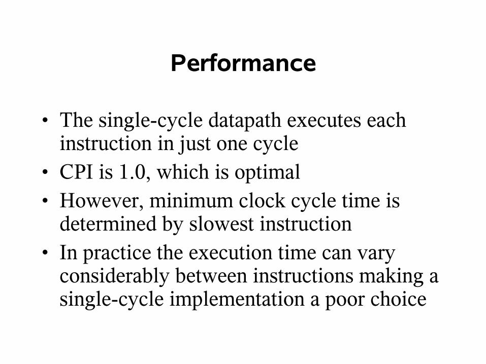
• The single-cycle datapath executes each instruction in just one cycle
• CPI is 1.0, which is optimal• However, minimum clock cycle time is
determined by slowest instruction• In practice the execution time can vary
considerably between instructions making a single-cycle implementation a poor choice

Using Multiple Cycles
• A multi-cycle datapath splits instruction execution into multiple steps, where each step take one cycle
• If an instruction doesn't need a step it skips it, so different instructions run for different numbers of cycles
• Slow instructions don't slow down the entire processor
• Control unit becomes more complicated• Hardware can be shared between steps

Multicycle Datapath (1)
PC
Memory
Address
Instruction or data
Data
Instruction register
Registers
Register #
Data
Register #
Register #
ALU
Memory data
register
A
B
ALUOut

Multicycle Differences
• A functional unit can be used more than once in the execution of an instruction, so long as those uses occur in different steps– Instruction memory and data memory are
combined into a single unit
– ALU takes over for the two separate adders
• Additional registers are needed to save information between steps

Multicycle Registers
• Instruction register (IR): hold the instruction during its execution
• Memory data register (MDR): hold the data read from memory for one cycle
• A: hold source register for one cycle
• B: hold source register for one cycle
• ALUOut: hold ALU output for one cycle

Multicycle Datapath (2)
Shift left 2
PC
Memory
MemData
Write data
M u x
0
1
RegistersWrite register
Write data
Read data 1
Read data 2
Read register 1
Read register 2
M u x
0
1
M u x
0
1
4
Instruction [15– 0]
Sign extend
3216
Instruction [25– 21]
Instruction [20– 16]
Instruction [15– 0]
Instruction register
1 M u x
0
3
2
M u x
ALU result
ALUZero
Memory data
register
Instruction [15– 11]
A
B
ALUOut
0
1
Address

Multicycle Datapath (3)
Shift left 2
MemtoReg
IorD MemRead MemWrite
PC
Memory
MemData
Write data
M u x
0
1
RegistersWrite register
Write data
Read data 1
Read data 2
Read register 1
Read register 2
Instruction [15– 11]
M u x
0
1
M u x
0
1
4
ALUOpALUSrcB
RegDst RegWrite
Instruction [15– 0]
Instruction [5– 0]
Sign extend
3216
Instruction [25– 21]
Instruction [20– 16]
Instruction [15– 0]
Instruction register
1 M u x
0
3
2
ALU control
M u x
0
1ALU
resultALU
ALUSrcA
ZeroA
B
ALUOut
IRWrite
Address
Memory data
register

New Control Signals
• ALUSrcA: selects first ALU operand to be either the PC or the A register
• ALUSrcB: selects second ALU operand from: B register, constant 4, sign-extended immediate, sign-extended and shifted immediate
• MemtoReg: selects register file write data as coming from either ALUOut or MDR
• IorD: selects the memory address as coming from either PC or ALUOut
New Control Signals (cont'd)
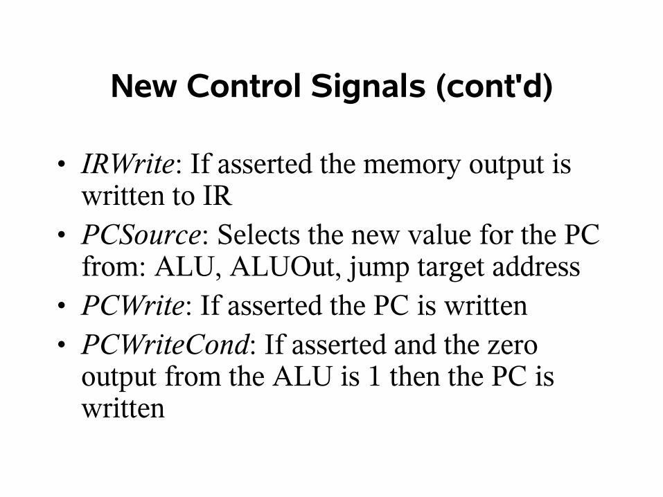
• IRWrite: If asserted the memory output is written to IR
• PCSource: Selects the new value for the PC from: ALU, ALUOut, jump target address
• PCWrite: If asserted the PC is written• PCWriteCond: If asserted and the zero
output from the ALU is 1 then the PC is written

Instruction Execution Steps
• Instruction fetch
• Instruction decode and register fetch
• Execution, memory address computation, or branch completion
• Memory access or R-type completion
• Memory read completion

Instruction Fetch
• Fetch instruction from memory– IR ← Memory[PC]
• Increment the PC– PC ← PC + 4

Instruction Decode
• Fetch operands from register file– A ← Reg[IR[25:21]]
– B ← Reg[IR[20:16]]
• Compute branch target address– ALUOut ← PC + (sign-extend(IR[15:0]) << 2)

Execute
• Load/store: Compute memory address– ALUOut ← A + sign-extend(IR[15:0])
• R-type: Perform operation specified by instruction– ALUOut ← A op B
• Branch: Compare registers and set PC if equal– if (A == B) PC ← ALUOut
• Jump: Set PC to jump target address– PC ← {PC[31:28], (IR[25:0] << 2)}

Memory Access
• Load: Read memory word into MDR– MDR ← Memory[ALUOut]
• Store: Write B into memory– Memory[ALUOut] ← B
• R-type: Write result to destination register– Reg[IR[15:11]] ← ALUOut

Memory Read Completion
• Load: Write result to destination register– Reg[IR[20:16]] ← MDR

Multicycle Datapath (4)
Shift left 2
PCM u x
0
1
RegistersWrite register
Write data
Read data 1
Read data 2
Read register 1
Read register 2
Instruction [15– 11]
M u x
0
1
M u x
0
1
4
Instruction [15– 0]
Sign extend
3216
Instruction [25– 21]
Instruction [20– 16]
Instruction [15– 0]
Instruction register
ALU control
ALU result
ALUZero
Memory data
register
A
B
IorD
MemRead
MemWrite
MemtoReg
PCWriteCond
PCWrite
IRWrite
ALUOp
ALUSrcB
ALUSrcA
RegDst
PCSource
RegWrite
Control
Outputs
Op [5– 0]
Instruction [31-26]
Instruction [5– 0]
M u x
0
2
Jump address [31-0]Instruction [25– 0] 26 28
Shift left 2
PC [31-28]
1
1 M u x
0
3
2
M u x
0
1ALUOut
Memory
MemData
Write data
Address

State Machine
• A state machine is a sequential logic device with:– Set of states
– Next-state function which determines the next state from the current state and the inputs
– Output function which determines the outputs from the current state and possibly the inputs
• In a Moore machine the output depends only on the state; in a Mealy machine the output depends on the state and the inputs

Control with a State Machine
• The control unit for our multicycle datapath will be a state machine
• The only input is the op field of the instruction; the outputs are the control signals
• Each step may have multiple states if control signals depend on the instruction
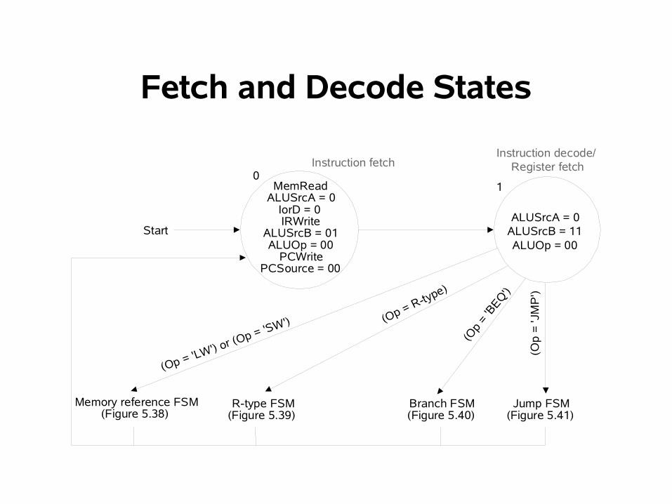
Fetch and Decode States
ALUSrcA = 0 ALUSrcB = 11 ALUOp = 00
MemRead ALUSrcA = 0
IorD = 0 IRWrite
ALUSrcB = 01 ALUOp = 00
PCWrite PCSource = 00
Instruction fetchInstruction decode/
Register fetch
(Op = 'LW') or (Op = 'SW') (Op = R-type)
(Op
= 'B
EQ')
(Op
= 'J
MP
')
01
Start
Memory reference FSM (Figure 5.38)
R-type FSM (Figure 5.39)
Branch FSM (Figure 5.40)
Jump FSM (Figure 5.41)

Load and Store States
MemWrite IorD = 1
MemRead IorD = 1
ALUSrcA = 1 ALUSrcB = 10 ALUOp = 00
RegWrite MemtoReg = 1
RegDst = 0
Memory address computation
(Op = 'LW') or (Op = 'SW')
Memory access
Write-back step
(Op = 'SW
')
(Op
= 'L
W')
4
2
53
From state 1
To state 0 (Figure 5.37)
Memory access

R-Type States
ALUSrcA = 1 ALUSrcB = 00 ALUOp = 10
RegDst = 1 RegWrite
MemtoReg = 0
Execution
R-type completion
6
7
(Op = R-type)
From state 1
To state 0 (Figure 5.37)

Branch State
Branch completion
8
(Op = 'BEQ')
From state 1
To state 0 (Figure 5.37)
ALUSrcA = 1 ALUSrcB = 00 ALUOp = 01 PCWriteCond
PCSource = 01
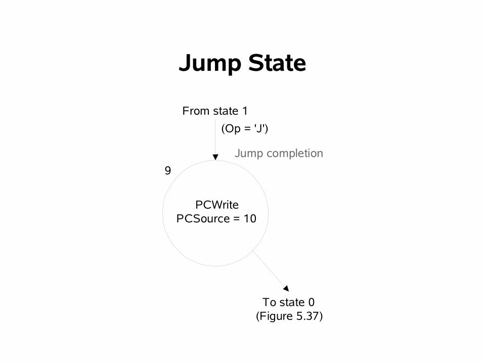
Jump State
Jump completion
9
(Op = 'J')
From state 1
To state 0 (Figure 5.37)
PCWrite PCSource = 10
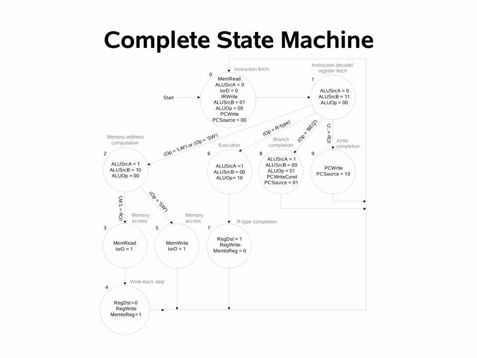
Complete State Machine
PCWrite PCSource = 10
ALUSrcA = 1 ALUSrcB = 00 ALUOp = 01 PCWriteCond
PCSource = 01
ALUSrcA =1 ALUSrcB = 00 ALUOp= 10
RegDst = 1 RegWrite
MemtoReg = 0
MemWrite IorD = 1
MemRead IorD = 1
ALUSrcA = 1 ALUSrcB = 10 ALUOp = 00
RegDst =0 RegWrite
MemtoReg =1
ALUSrcA = 0 ALUSrcB = 11 ALUOp = 00
MemRead ALUSrcA = 0
IorD = 0 IRWrite
ALUSrcB = 01 ALUOp = 00
PCWrite PCSource = 00
Instruction fetchInstruction decode/
register fetch
Jump completion
Branch completionExecution
Memory address computation
Memory access
Memory access R-type completion
Write-back step
(Op = 'LW') or (Op = 'SW') (Op = R-type)
(Op
= 'B
EQ')
(Op
= 'J
') (O
p = 'SW')
(Op
= 'L
W')
4
01
9862
753
Start