Embed Size (px)
Citation preview
Computational Modeling Module: Electronic Band Structure Calculations
MSE 410, 10/03 & 10/5
Learning Outcomes and Topics Learning outcomes:
– Get familiar with density functional theory (DFT) and simulation procedure.
– Prepare your own computational modeling input files. – Apply the DFT simulation method to calculate band structure and
explore band gap and alignment. – Determine “physical validity” of calculation by comparing the
simulated band diagram to what has been published in the literature. What to simulate:
– Materials: Graphene with point defects and dopants – Band Structure – Electronic band engineering to control band gap size and alignment
Assessment: – Reading HW – Modeling HW
2

Reading / Self-Studying Resources
• Video # 1: Intro to Computational Modeling https://www.youtube.com/watch?v=4J6aStfuJAU
• Video # 2: Input Parameters for SIESTA Simulation https://www.youtube.com/watch?v=AVkQkNpzxio
• Must-remember notes for DFT • LeSar Chapter 4 Electronic Structure Methods • I will grade your reading HW and return to you in
the next class.
3
nanoHUB
• Register at https://nanohub.org/register/ • Login to your account • On “My Tools”, select “MIT Atomic Scale
Modeling Toolkit” as your “Favorites” tool. • Launch “MIT Atomic Scale Modeling Toolkit”
to run SIESTA
4
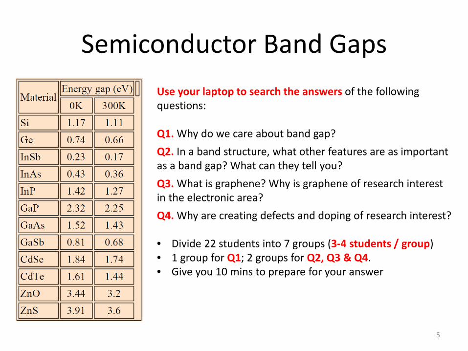
Semiconductor Band Gaps Use your laptop to search the answers of the following questions: Q1. Why do we care about band gap? Q2. In a band structure, what other features are as important as a band gap? What can they tell you? Q3. What is graphene? Why is graphene of research interest in the electronic area? Q4. Why are creating defects and doping of research interest? • Divide 22 students into 7 groups (3-4 students / group) • 1 group for Q1; 2 groups for Q2, Q3 & Q4. • Give you 10 mins to prepare for your answer
5
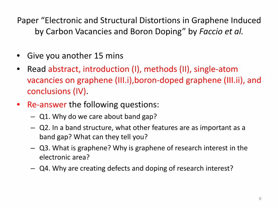
Paper “Electronic and Structural Distortions in Graphene Induced by Carbon Vacancies and Boron Doping” by Faccio et al.
• Give you another 15 mins • Read abstract, introduction (I), methods (II), single-atom
vacancies on graphene (III.i),boron-doped graphene (III.ii), and conclusions (IV).
• Re-answer the following questions: – Q1. Why do we care about band gap? – Q2. In a band structure, what other features are as important as a
band gap? What can they tell you? – Q3. What is graphene? Why is graphene of research interest in the
electronic area? – Q4. Why are creating defects and doping of research interest?
6
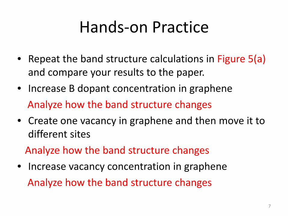
Hands-on Practice
• Repeat the band structure calculations in Figure 5(a) and compare your results to the paper.
• Increase B dopant concentration in graphene Analyze how the band structure changes • Create one vacancy in graphene and then move it to
different sites Analyze how the band structure changes • Increase vacancy concentration in graphene Analyze how the band structure changes
7
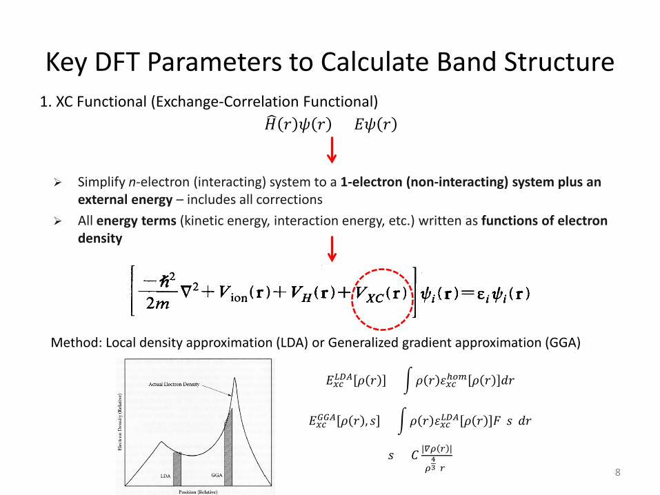
Key DFT Parameters to Calculate Band Structure 1. XC Functional (Exchange-Correlation Functional)
𝐻𝐻� 𝑟𝑟 𝜓𝜓 𝑟𝑟 = 𝐸𝐸𝜓𝜓 𝑟𝑟
Simplify n-electron (interacting) system to a 1-electron (non-interacting) system plus an external energy – includes all corrections
All energy terms (kinetic energy, interaction energy, etc.) written as functions of electron density
Method: Local density approximation (LDA) or Generalized gradient approximation (GGA)
𝐸𝐸𝑥𝑥𝑥𝑥𝐿𝐿𝐿𝐿𝐿𝐿 𝜌𝜌 𝑟𝑟 = �𝜌𝜌 𝑟𝑟 𝜀𝜀𝑥𝑥𝑥𝑥ℎ𝑜𝑜𝑜𝑜 𝜌𝜌 𝑟𝑟 𝑑𝑑𝑟𝑟
𝐸𝐸𝑥𝑥𝑥𝑥𝐺𝐺𝐺𝐺𝐿𝐿 𝜌𝜌 𝑟𝑟 , 𝑠𝑠 = �𝜌𝜌 𝑟𝑟 𝜀𝜀𝑥𝑥𝑥𝑥𝐿𝐿𝐿𝐿𝐿𝐿 𝜌𝜌 𝑟𝑟 𝐹𝐹(𝑠𝑠)𝑑𝑑𝑟𝑟
𝑠𝑠 = 𝐶𝐶 |𝛻𝛻𝛻𝛻 𝑟𝑟 |
𝛻𝛻43(𝑟𝑟)
8
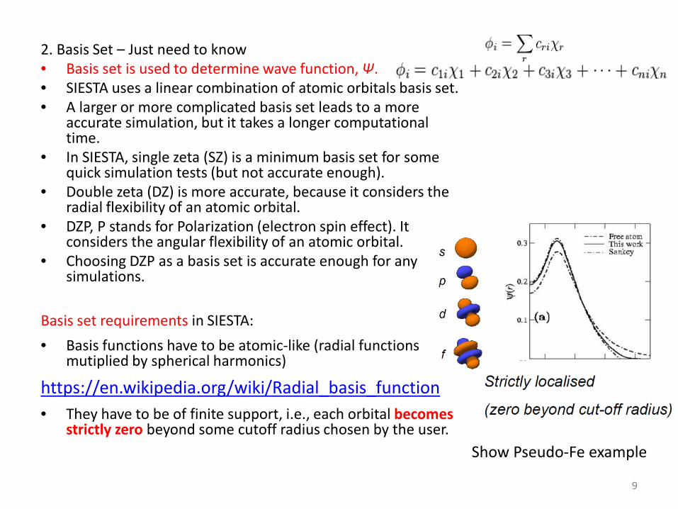
2. Basis Set – Just need to know • Basis set is used to determine wave function, Ψ. • SIESTA uses a linear combination of atomic orbitals basis set. • A larger or more complicated basis set leads to a more
accurate simulation, but it takes a longer computational time.
• In SIESTA, single zeta (SZ) is a minimum basis set for some quick simulation tests (but not accurate enough).
• Double zeta (DZ) is more accurate, because it considers the radial flexibility of an atomic orbital.
• DZP, P stands for Polarization (electron spin effect). It considers the angular flexibility of an atomic orbital.
• Choosing DZP as a basis set is accurate enough for any simulations.
Basis set requirements in SIESTA: • Basis functions have to be atomic-like (radial functions
mutiplied by spherical harmonics)
https://en.wikipedia.org/wiki/Radial_basis_function • They have to be of finite support, i.e., each orbital becomes
strictly zero beyond some cutoff radius chosen by the user.
Show Pseudo-Fe example
9
3. Mesh cutoff – Just need to know • In SIESTA, mesh cutoff is an energy (default 100 Ry), which corresponds to
a finite 3D grid for the calculation of electron density ρ(𝑟𝑟) and potentials. • Note that electron density is a function of position. We need to define the
spacing of this 3D grid to map the electron density. • Larger mesh cutoff ⇒ smaller spacing ⇒ more dense 3D mesh ⇒ more
accurate simulation but longer computational time.
10
k-Point Density / Sampling in Brillouin Zone
Any point in the Irreducible Brillouin zone can represent a k-point, there are an infinite number of discrete k-vectors well qualified to be a wave function. The wave function and other properties vary smoothly over the IBZ, so we can just sample a finite number of k-points that represent each small region. Choose k-points: • Big system vs. small system • Isolated molecule • Symmetric system
11
Brillouin zone & k-point sampling Go through http://www.doitpoms.ac.uk/tlplib/brillouin_zones/intro.php
– Introduction – Reciprocal lattice vectors – Brillouin zone construction – The general case in three dimensions – Zone folding – Examples of Brillouin Zones in three Dimensions
12
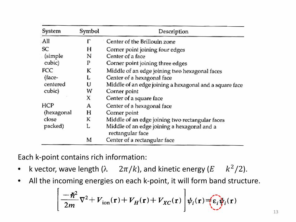
Each k-point contains rich information: • k vector, wave length (λ = 2𝜋𝜋/𝑘𝑘), and kinetic energy (𝐸𝐸 = 𝑘𝑘2/2). • All the incoming energies on each k-point, it will form band structure.
13
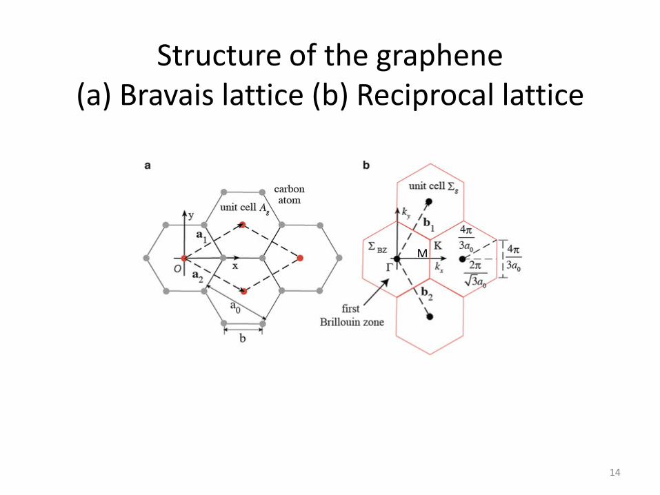
Structure of the graphene (a) Bravais lattice (b) Reciprocal lattice
M
14
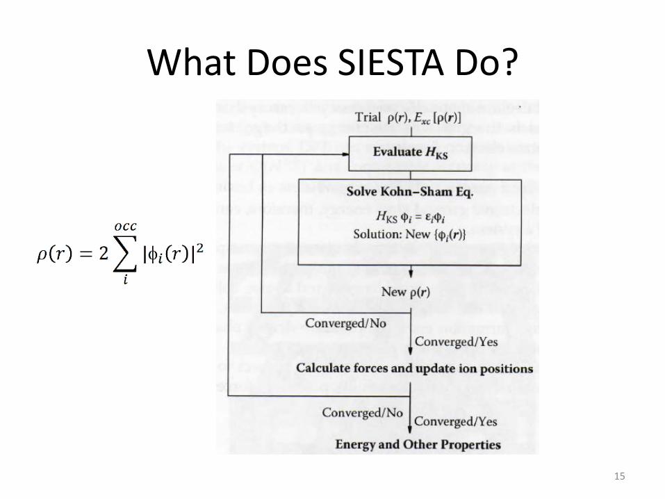
What Does SIESTA Do?
15
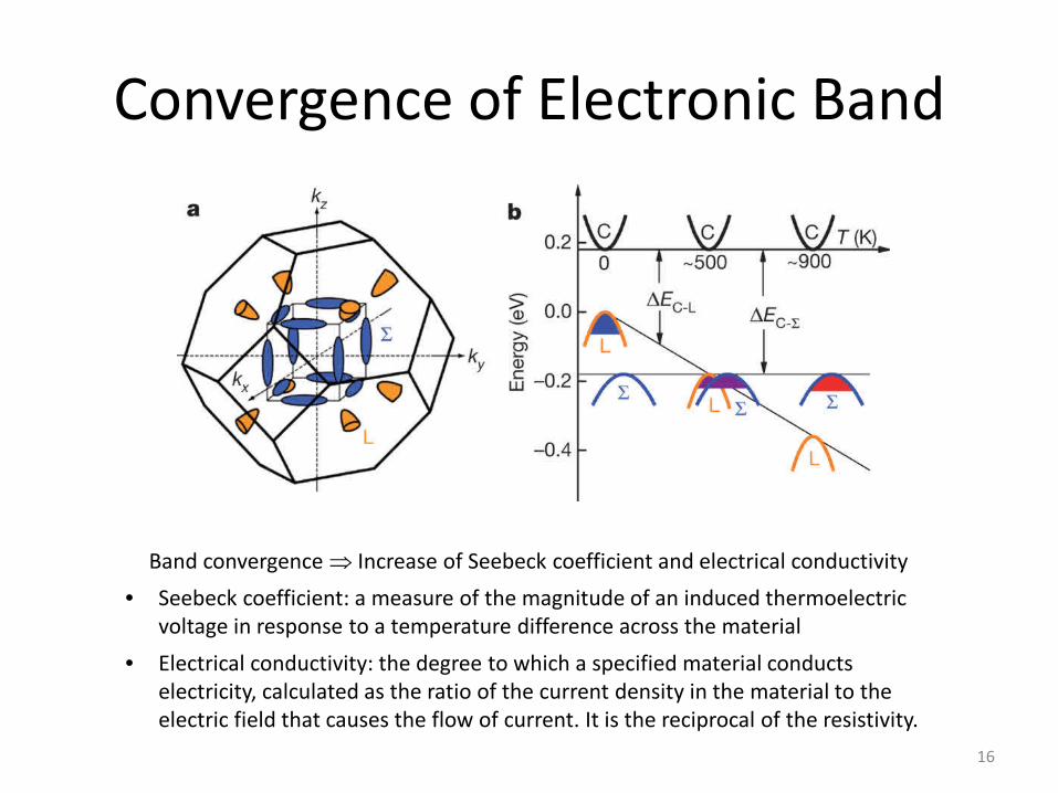
Convergence of Electronic Band
Band convergence ⇒ Increase of Seebeck coefficient and electrical conductivity • Seebeck coefficient: a measure of the magnitude of an induced thermoelectric
voltage in response to a temperature difference across the material • Electrical conductivity: the degree to which a specified material conducts
electricity, calculated as the ratio of the current density in the material to the electric field that causes the flow of current. It is the reciprocal of the resistivity.
16
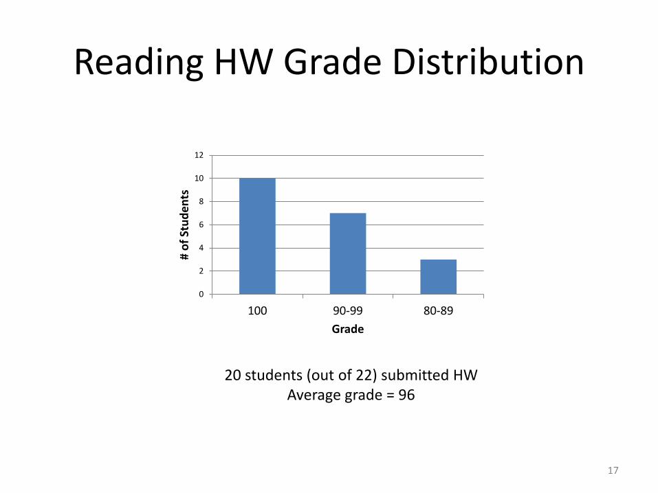
Reading HW Grade Distribution
17
20 students (out of 22) submitted HW Average grade = 96
0
2
4
6
8
10
12
100 90-99 80-89
# of
Stu
dent
s
Grade
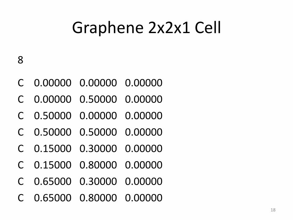
Graphene 2x2x1 Cell
8
C 0.00000 0.00000 0.00000 C 0.00000 0.50000 0.00000 C 0.50000 0.00000 0.00000 C 0.50000 0.50000 0.00000 C 0.15000 0.30000 0.00000 C 0.15000 0.80000 0.00000 C 0.65000 0.30000 0.00000 C 0.65000 0.80000 0.00000
18

Take-Home Exercise • Literature review:
– What other point defects and dopants in graphene are of research interest?
– Why? – Any potential applications?
• Modeling HW (Email to me [email protected] by Fri, Oct 13) Based on what you find in literature:
– Choose one defect or one dopant – Calculate its band structure – Analyze your results – Write a two-page report, including introduction, motivation (why are
you interested in that type of defect / dopant), results and discussion (including band structure figures), conclusion, and references
19