Embed Size (px)
Citation preview
Air Force Institute of TechnologyAFIT Scholar
Theses and Dissertations Student Graduate Works
3-14-2014
Complex VLSI Feature Comparison forCommercial Microelectronics VerificationMichael K. Seery
Follow this and additional works at: https://scholar.afit.edu/etd
This Thesis is brought to you for free and open access by the Student Graduate Works at AFIT Scholar. It has been accepted for inclusion in Theses andDissertations by an authorized administrator of AFIT Scholar. For more information, please contact [email protected].
Recommended CitationSeery, Michael K., "Complex VLSI Feature Comparison for Commercial Microelectronics Verification" (2014). Theses andDissertations. 623.https://scholar.afit.edu/etd/623

COMPLEX VLSI FEATURE COMPARISON FOR COMMERCIAL
MICROELECTRONICS VERIFICATION
THESIS
Michael K. Seery, Second Lieutenant, USAF
AFIT-ENG-14-M-67
DEPARTMENT OF THE AIR FORCEAIR UNIVERSITY
AIR FORCE INSTITUTE OF TECHNOLOGY
Wright-Patterson Air Force Base, Ohio
DISTRIBUTION STATEMENT A:
APPROVED FOR PUBLIC RELEASE; DISTRIBUTION UNLIMITED

The views expressed in this thesis are those of the author and do not reflect the official
policy or position of the United States Air Force, the Department of Defense, or the
United States Government.
This material is declared a work of the U.S. Government and is not subject to copyright
protection in the United States.

AFIT-ENG-14-M-67
COMPLEX VLSI FEATURE COMPARISON FOR COMMERCIAL
MICROELECTRONICS VERIFICATION
THESIS
Presented to the Faculty
Department of Electrical and Computer Engineering
Graduate School of Engineering and Management
Air Force Institute of Technology
Air University
Air Education and Training Command
in Partial Fulfillment of the Requirements for the
Degree of Master of Science in Computer Engineering
Michael K. Seery, B.S.C.E.
Second Lieutenant, USAF
March 2014
DISTRIBUTION STATEMENT A:
APPROVED FOR PUBLIC RELEASE; DISTRIBUTION UNLIMITED

AFIT-ENG-14-M-67
COMPLEX VLSI FEATURE COMPARISON FOR COMMERCIAL
MICROELECTRONICS VERIFICATION
Michael K. Seery, B.S.C.E.
Second Lieutenant, USAF
Approved:
//signed//
Mary Y. Lanzerotti, PhD (Chairman)
//signed//
Kenneth M. Hopkinson, PhD (Member)
//signed//
Maj Samuel J. Stone, PhD (Member)
6 Mar 2014
Date
5 Mar 2014
Date
5 Mar 2014
Date

AFIT-ENG-14-M-67Abstract
Shortcomings in IC verification make for glaring vulnerabilities in the form of
hardware backdoors, or extraneous operation modes that allow unauthorized, undetected
access. The DARPA TRUST program addressed the need for verification of untrusted
circuits using industry-standard and custom software. The process developed under
TRUST and implemented at the AFRL Mixed Signal Design Center has not been tested
using real-world circuits outside of the designated TRUST test cases.
This research demonstrates the potential of applying software designed for TRUST
test articles on microchips from questionable sources. A specific process is developed for
both transistor-level library cell verification and gate-level circuit verification. The relative
effectiveness and scalability of the process are assessed.
iv
Acknowledgments
Sincere appreciation is due to Dr. Mary Lanzerotti for continued guidance as advisor
and committee chair. Also deserving of recognition are Dr. Ken Hopkinson and Dr.
Samuel Stone at the Air Force Institute of Technology for serving as committee members
on this research, and Mr. Brad Paul, Mr. Len Orlando, Dr. Michael Myers, Dr. Brian
Dupaix and Mr. Dave Lucking at AFRL MSDC for their advice, teaching and research
contributions.
Michael K. Seery
v

Table of Contents
Page
Abstract . . . . . . . . . . . . . . . . . . . . . . . . . . . . . . . . . . . . . . . . . iv
Acknowledgments . . . . . . . . . . . . . . . . . . . . . . . . . . . . . . . . . . . . v
Table of Contents . . . . . . . . . . . . . . . . . . . . . . . . . . . . . . . . . . . . vi
List of Figures . . . . . . . . . . . . . . . . . . . . . . . . . . . . . . . . . . . . . . ix
List of Tables . . . . . . . . . . . . . . . . . . . . . . . . . . . . . . . . . . . . . . xi
List of Acronyms . . . . . . . . . . . . . . . . . . . . . . . . . . . . . . . . . . . . xii
I. Introduction . . . . . . . . . . . . . . . . . . . . . . . . . . . . . . . . . . . . . 1
1.1 Trust . . . . . . . . . . . . . . . . . . . . . . . . . . . . . . . . . . . . . . 2
1.2 Research Problem . . . . . . . . . . . . . . . . . . . . . . . . . . . . . . . 3
1.3 Justification . . . . . . . . . . . . . . . . . . . . . . . . . . . . . . . . . . 3
1.4 DARPA Trusted Integrated Circuits (TRUST) . . . . . . . . . . . . . . . . 4
1.5 Proposed Methodology . . . . . . . . . . . . . . . . . . . . . . . . . . . . 5
1.6 Assumptions and Scope . . . . . . . . . . . . . . . . . . . . . . . . . . . . 6
1.7 Materials and Equipment . . . . . . . . . . . . . . . . . . . . . . . . . . . 6
II. Background . . . . . . . . . . . . . . . . . . . . . . . . . . . . . . . . . . . . . 8
2.1 Microchip Acquisition . . . . . . . . . . . . . . . . . . . . . . . . . . . . 8
2.2 Trusted Foundries . . . . . . . . . . . . . . . . . . . . . . . . . . . . . . . 12
2.3 Threats . . . . . . . . . . . . . . . . . . . . . . . . . . . . . . . . . . . . 16
2.4 Impact . . . . . . . . . . . . . . . . . . . . . . . . . . . . . . . . . . . . . 20
2.5 Response . . . . . . . . . . . . . . . . . . . . . . . . . . . . . . . . . . . 22
2.6 DARPA TRUST . . . . . . . . . . . . . . . . . . . . . . . . . . . . . . . . 23
2.7 Conclusion . . . . . . . . . . . . . . . . . . . . . . . . . . . . . . . . . . 28
III. Methodology . . . . . . . . . . . . . . . . . . . . . . . . . . . . . . . . . . . . 29
3.1 Introduction . . . . . . . . . . . . . . . . . . . . . . . . . . . . . . . . . . 29
3.2 TRUST at Air Force Research Laboratory (AFRL) . . . . . . . . . . . . . 30
3.3 Test Methodology . . . . . . . . . . . . . . . . . . . . . . . . . . . . . . . 32
3.3.1 Cell Recognition . . . . . . . . . . . . . . . . . . . . . . . . . . . 37
vi

Page
3.3.2 Enhanced Design Rule Check . . . . . . . . . . . . . . . . . . . . 38
3.3.3 Timing Check . . . . . . . . . . . . . . . . . . . . . . . . . . . . . 38
3.3.4 Hierarchical Extraction / TRUST Structural Database . . . . . . . . 39
3.3.5 Equivalence Check & Advanced Mapping . . . . . . . . . . . . . . 40
3.3.6 Exploitable Logic Check . . . . . . . . . . . . . . . . . . . . . . . 40
3.3.7 Conformal for Custom Layouts . . . . . . . . . . . . . . . . . . . 41
3.3.7.1 Transistor-Level . . . . . . . . . . . . . . . . . . . . . . 41
3.3.7.2 Gate-Level . . . . . . . . . . . . . . . . . . . . . . . . . 41
IV. Results . . . . . . . . . . . . . . . . . . . . . . . . . . . . . . . . . . . . . . . . 43
4.1 Transistor-level Testing . . . . . . . . . . . . . . . . . . . . . . . . . . . . 43
4.1.1 Preliminary Results with Circuit A . . . . . . . . . . . . . . . . . . 43
4.1.1.1 Generation . . . . . . . . . . . . . . . . . . . . . . . . . 43
4.1.1.2 Verification . . . . . . . . . . . . . . . . . . . . . . . . 47
4.1.2 Further experimentation with Circuit A . . . . . . . . . . . . . . . 50
4.1.2.1 Serial ordering . . . . . . . . . . . . . . . . . . . . . . . 51
4.1.2.2 NC-Verilog drain-source assignment . . . . . . . . . . . 53
4.2 Gate-level Testing . . . . . . . . . . . . . . . . . . . . . . . . . . . . . . . 59
4.2.1 Circuit B . . . . . . . . . . . . . . . . . . . . . . . . . . . . . . . 59
4.2.1.1 Generation . . . . . . . . . . . . . . . . . . . . . . . . . 59
4.2.1.2 Verification . . . . . . . . . . . . . . . . . . . . . . . . 63
4.2.2 Circuit C . . . . . . . . . . . . . . . . . . . . . . . . . . . . . . . 65
4.2.3 Circuit D . . . . . . . . . . . . . . . . . . . . . . . . . . . . . . . 66
4.2.3.1 Generation . . . . . . . . . . . . . . . . . . . . . . . . . 66
4.2.3.2 Verification . . . . . . . . . . . . . . . . . . . . . . . . 69
4.2.4 Circuit E . . . . . . . . . . . . . . . . . . . . . . . . . . . . . . . 74
4.3 Summary . . . . . . . . . . . . . . . . . . . . . . . . . . . . . . . . . . . 77
V. Conclusion and Future Work . . . . . . . . . . . . . . . . . . . . . . . . . . . . 78
5.1 Summary . . . . . . . . . . . . . . . . . . . . . . . . . . . . . . . . . . . 78
5.2 Future Work . . . . . . . . . . . . . . . . . . . . . . . . . . . . . . . . . . 78
5.2.1 Circuit A − 1 . . . . . . . . . . . . . . . . . . . . . . . . . . . . . 79
5.2.2 Circuit A + 1 . . . . . . . . . . . . . . . . . . . . . . . . . . . . . 79
5.2.3 SCR and Other Netlists . . . . . . . . . . . . . . . . . . . . . . . . 79
5.2.4 Additional Tools . . . . . . . . . . . . . . . . . . . . . . . . . . . 80
5.2.5 Circuit Prototype E2 and Further Complexity Scaling (Circuit F) . . 80
5.2.6 Fabrication . . . . . . . . . . . . . . . . . . . . . . . . . . . . . . 81
5.3 Conclusion . . . . . . . . . . . . . . . . . . . . . . . . . . . . . . . . . . 81
vii

Page
Bibliography . . . . . . . . . . . . . . . . . . . . . . . . . . . . . . . . . . . . . . 82
viii
List of Figures
Figure Page
1 Total reported or suspected hardware counterfeits, 2005-2008 [9]. . . . . . . . 14
2 Companies reporting suspected or confirmed counterfeit microcircuits, by type
[9]. . . . . . . . . . . . . . . . . . . . . . . . . . . . . . . . . . . . . . . . . . 15
3 Functional test on example adder [5]. . . . . . . . . . . . . . . . . . . . . . . . 26
4 Transistor-level test on example adder[5]. . . . . . . . . . . . . . . . . . . . . 27
5 TRUST tools forward design flow [33]. . . . . . . . . . . . . . . . . . . . . . 30
6 Standard and reverse EDA design methodologies (Adapted from [25]). . . . . . 32
7 Netlist matching toolflow. . . . . . . . . . . . . . . . . . . . . . . . . . . . . . 37
8 Iterative netlist matching process [33]. . . . . . . . . . . . . . . . . . . . . . . 40
9 Conceptual process for preliminary results. . . . . . . . . . . . . . . . . . . . 44
10 Circuit A layout. . . . . . . . . . . . . . . . . . . . . . . . . . . . . . . . . . 44
11 Circuit A initial schematic. . . . . . . . . . . . . . . . . . . . . . . . . . . . . 45
12 Comparison of initial Circuit A layout (left) and schematic (right) netlists as
generated by Cadence software. . . . . . . . . . . . . . . . . . . . . . . . . . 46
13 Processing Circuit A for Verification. . . . . . . . . . . . . . . . . . . . . . . . 48
14 VDD, GND and Z points unmapped by Cadence Conformal. . . . . . . . . . . 49
15 Circuit A logical blocks . . . . . . . . . . . . . . . . . . . . . . . . . . . . . . 51
16 Circuit A block 1 PMOS schematic before and after serial order corrections. . . 52
17 Circuit A block 1 PMOS transistors showing ordered series layout. . . . . . . . 53
18 Circuit A netlist directed graphs, with legend . . . . . . . . . . . . . . . . . . 56
19 Left-to-Right Schematic. . . . . . . . . . . . . . . . . . . . . . . . . . . . . . 57
20 Left-to-Right Layout. . . . . . . . . . . . . . . . . . . . . . . . . . . . . . . . 57
ix

Figure Page
21 Representative Left-to-Right Netlist Modification. Green indicates drains
changed to sources; Red indicates the opposite. . . . . . . . . . . . . . . . . . 58
22 Circuit B VHDL code. . . . . . . . . . . . . . . . . . . . . . . . . . . . . . . 59
23 Circuit B RTL Compiler TCL script. . . . . . . . . . . . . . . . . . . . . . . . 61
24 Circuit B Verilog code. . . . . . . . . . . . . . . . . . . . . . . . . . . . . . . 62
25 A symbolic schematic of Circuit B, the clocked inverter. . . . . . . . . . . . . 62
26 The Assura LVS GUI, configured to incrementally verify Circuit B. . . . . . . 62
27 Conformal showing mapped points in Circuit B. . . . . . . . . . . . . . . . . . 63
28 Processing Circuit B for Verification. . . . . . . . . . . . . . . . . . . . . . . . 64
29 A symbolic schematic of Circuit C at the top level. . . . . . . . . . . . . . . . 66
30 VHDL for Circuit D. . . . . . . . . . . . . . . . . . . . . . . . . . . . . . . . 67
31 A schematic of the single-cell Circuit Prototype D1. . . . . . . . . . . . . . . . 67
32 Circuit D Tcl script modifications for Circuit Prototype D2. . . . . . . . . . . . 68
33 A schematic of the complex Circuit Prototype D2. . . . . . . . . . . . . . . . . 68
34 Circuit D Tcl script modifications for Circuit Prototype D3. . . . . . . . . . . . 69
35 A schematic of Circuit Prototype D3. . . . . . . . . . . . . . . . . . . . . . . . 69
36 Assura layout versus schematic (LVS) showing successful results for Circuit D. 70
37 Cadence Encounter script to initialize, floorplan, place, route and export Circuit
D. . . . . . . . . . . . . . . . . . . . . . . . . . . . . . . . . . . . . . . . . . 72
38 Cadence Virtuoso graphical user interface (GUI) showing stream-in configura-
tion for Circuit D. . . . . . . . . . . . . . . . . . . . . . . . . . . . . . . . . . 73
x
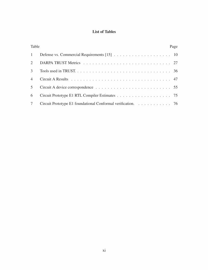
List of Tables
Table Page
1 Defense vs. Commercial Requirements [15] . . . . . . . . . . . . . . . . . . . 10
2 DARPA TRUST Metrics . . . . . . . . . . . . . . . . . . . . . . . . . . . . . 27
3 Tools used in TRUST. . . . . . . . . . . . . . . . . . . . . . . . . . . . . . . . 36
4 Circuit A Results . . . . . . . . . . . . . . . . . . . . . . . . . . . . . . . . . 47
5 Circuit A device correspondence . . . . . . . . . . . . . . . . . . . . . . . . . 55
6 Circuit Prototype E1 RTL Compiler Estimates . . . . . . . . . . . . . . . . . . 75
7 Circuit Prototype E1 foundational Conformal verification. . . . . . . . . . . . 76
xi

List of Acronyms
Acronym Definition
AES Advanced Encryption Standard
AFB Air Force base
AFRL Air Force Research Laboratory
AFIT the Air Force Institute of Technology
ASIC application-specific integrated circuit
CAD computer-aided design
CMOS complementary metal-oxide semiconductor
CMP chemical-mechanical polishing
COTS commercial off-the-shelf
DARPA Defense Advanced Research Projects Agency
DMEA Defense Microelectronics Activity
DoD Department of Defense
DoS denial of service
DoDI Department of Defense instruction
DSB Defense Science Board
DTICS Defense Trusted Integrated Circuit Strategy
EDA electronic design automation
FIB focused ion beam
FLIR forward-looking infrared
GDSII Graphical Design System II
GUI graphical user interface
HDL hardware description language
HIP hard intellectual property
xii

Acronym Definition
IARPA Intelligence Advanced Research Projects Activity
IBM International Business Machines Corporation
I2C Inter-Integrated Circuit
IC integrated circuit
I/O input/output
IP intellectual property
IRIS Integrity and Reliability of Integrated Circuits
LVS layout versus schematic
MOSIS the Metal Oxide Semiconductor Implementation Service
MSDC Mixed Signal Design Center
MTO Microsystems Technology Office
NCSU North Carolina State University
NIST National Institute of Standards and Technology
NP non-deterministic polynomial-time
OA OpenAccess
PDK process design kit
QC Quality Control
RTL register transfer language
SCR standard cell recognition
SEMATECH the Semiconductor Manufacturing Technology Consortium
TAPO the Trusted Access Program Office
Tcl Tool Command Language
TiF trust in fabrication
TF Trusted Foundry
TSDB TRUST structural database
xiii
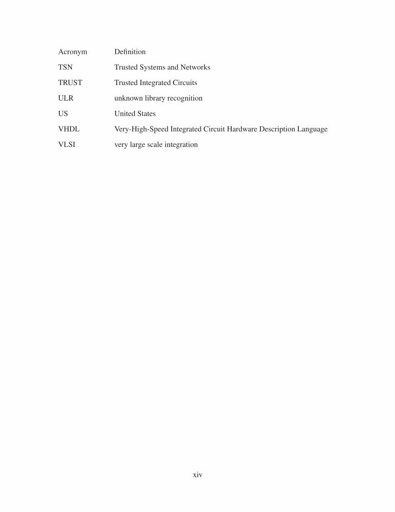
Acronym Definition
TSN Trusted Systems and Networks
TRUST Trusted Integrated Circuits
ULR unknown library recognition
US United States
VHDL Very-High-Speed Integrated Circuit Hardware Description Language
VLSI very large scale integration
xiv

COMPLEX VLSI FEATURE COMPARISON FOR COMMERCIAL
MICROELECTRONICS VERIFICATION
I. Introduction
Defense related very large scale integration (VLSI) circuits are typically low-volume
products that are not highly profitable for commercial manufacturers [5].
However, the degree of technological specialization required to produce them requires
contracting of commercial foundries [8]. Furthermore, the migration of previously
domestic foundries to international markets due to economic incentives raises issues of
trust. Recent events have brought these issues more to light: an early article on threats
arising from breaches of trust appeared in BusinessWeek in 2008 [16]. Similar articles
have been written more recently outlining the nature of the trust challenge from the
civilian perspective [31].
The Department of Defense (DoD) depends on a reliable supply of custom hardware
[12]. However, the demand presented is small in volume compared to the demand for
commercial circuits - in most cases, military order sizes are one one-thousandth or less of
a comparable commercial order [15]. Furthermore, custom defense hardware has a strict
set of specifications beyond commercial chip requirements for environmental factors,
reliability and useful life [24]. Not only must the supply chain provide functional, trusted
hardware, but it also must be competitive with available commercial technologies [8]. The
disparity is surmountable, but a 2005 report by the Office of the Secretary of Defense
identified addressing the challenge to be both difficult and critically necessary to
overcome in the interest of national security.
1
1.1 Trust
The largest complicating factor, however, is trust. “Trust” has a very specific
definition when referencing DoD “trusted” suppliers. Trust in the context of electronic
hardware and information processing, as provided to National Semiconductor Corporation
(now Texas Instruments, Inc.), refers to:
“the ability of the Department of Defense to have confidence that a system
functions as intended and is free of exploitable vulnerabilities, either
intentionally or unintentionally designed or inserted as part of the system at
any time during its life cycle.” [3]
This statement was intended as a definition of trusted software, and it was composed
by the DoD for its Trusted Software Initiative. Given the commonality between the
software and hardware trust challenges, is a valid extrapolation [20].
The Defense Trusted Integrated Circuit Strategy (DTICS) memorandum dated 10
October 2003 initiated the programmatic changes that have occurred that led to the
founding of the Trusted Foundry (TF) program. It cites requirements for facility and
product identification (that is, the clearance, capacity and capability of trusted foundries),
near-term acquisition solutions and research initiatives to ensure a healthy domestic
integrated circuit (IC) market [11]. As it is defined in the memorandum, trust is the ability
to certify that designs sensitive to national security concerns are secure in the hands of a
commercial manufacturer [11].
A final definition of trust, for these purposes, comes from former Acting Under
Secretary of Defense for Acquisition, Technology, and Logistics Michael Wynne, who
stated in 2004 that trust is “the confidence in one’s ability to secure national security
systems by assessing the integrity of the people and processes used to design, generate,
manufacture, and distribute national security critical components” [34].
Since the challenges of volume and performance have made DoD production
facilities fiscally untenable, private contractors have been handed the task of fabricating
2

the United States (US) military’s ICs. This privatization presents a security challenge that
is difficult to address [22]. Due to financial incentives, many corporations now rely on
overseas foundries, further exacerbating the issue. Domestic trust is difficult enough;
placing a high degree of trust in foreign owned and operated foundries is an undesirable
position for the DoD due to the increased opportunities for tampering and counterfeiting
outside the United States [8].
1.2 Research Problem
ICs are difficult to verify at the individual device level. Shortcomings in IC
verification make for glaring vulnerabilities in the form of hardware backdoors, or
extraneous operation modes that allow unauthorized, undetected access [28]. A circuit
could be ordered that has a certain function, and appears functional, but has a device that
popular media have dubbed a “kill switch” [1] such that an adversary could disable it at a
crucial moment. The problem of verifying circuits is so difficult that the Defense
Advanced Research Projects Agency (DARPA) has funded two programs to enhance DoD
verification and reverse engineering capabilities. These two programs are TRUST and
Integrity and Reliability of Integrated Circuits (IRIS). Furthermore, DARPA’s intelligence
community analog, Intelligence Advanced Research Projects Activity (IARPA), has
funded a sister program to consider the intelligence aspects of using private foundries.
1.3 Justification
A threat is not significant unless it carries with it an impact. The potential for
compromised microelectronics to impact defense systems, at small and large scales, is
undeniable and significant. Defense technology frequently prevents loss of life, and
facilitates the judicious application of force. It follows that verification of defense
microelectronics is critical to national defense [8].
3
In a letter to members of the US Senate Committee on Armed Forces, Moshe
Gavrielov (President and CEO of Xilinx) noted that counterfeit parts present not only an
immediate threat, but also a prolonged one [14]. Such parts can be likened to a time bomb,
poised to cripple a system unexpectedly.
The same Senate Committee released a report on counterfeit electronic parts which
noted that exact prediction of the impact of failing electronics is in fact a difficult problem.
Often, commercial-grade components are illegally remarked to bear military-grade
designations. These parts may not fail until subjected to environmental stresses outside
the normal, commercial specification [6]. It is probable that the moment at which a device
is most stressed is the same moment it will be most crucial - an observation acceded by
the President of the Semiconductor Industry Association, Brian Toohey [29].
1.4 DARPA TRUST
As part of a multifaceted national response to these potential vulnerabilities, DARPA,
in 2007, issued contracts in support of a new program known as TRUST. This program set
a tiered schedule for contractors to pursue competitively, and provided development
funding. The goal was to develop the capability to match a physical device with the
register transfer language (RTL) that was used to create it, demonstrating that all
components are included and no extraneous devices exist. DARPA TRUST emphasizes
the weak links in the supply chain that could be introduced by untrusted manufacturing
facilities, and attempts to provide another option than foundry verification in obtaining
trusted products. Testing on chips as directed by the program requires performance to
design specifications, at a minimum, and not to exceed those specifications in a way that
adds unintended functionality. These specifications includes mitigating the risk of
modified hardware on the chip as well as interference from microchip peripherals such as
packaging, circuit integration and radio sidechannels. It also addresses the threat of chip
4

modification after installation, and attempts to provide a means of assessing such a
condition.
This research intends to increase the capability of the DoD to conduct feature
extraction on integrated circuits in support of DARPA TRUST and IRIS. This capability is
valuable to the intelligence community as well as for the test and evaluation of
commercial off-the-shelf (COTS) circuits for defense applications currently acquired
through the Trusted Access Program Office (TAPO) and the TF program.
1.5 Proposed Methodology
This research builds on previous algorithms implemented in software by contractors
in pursuit of the DARPA TRUST program. The candidate selected came from Raytheon,
but testing has not been performed on it using real-world circuits outside of the TRUST
test cases. Adaptive, a contractor specializing in workflow documentation, has been hired
to reestablish, document and automate the existing feature matching and comparison
process. This research will build on the existing toolset by investigating success and
failure cases of the software across various inputs, ranging from trivial to complex, and
attempt to expand those capabilities.
Complex digital designs, found by survey of available, licensed sources, will be
synthesized using the Cadence Encounter Suite to generate a unique set of test cases that
will explore the limits of the TRUST tools in both transistor count and standard cell usage.
The intellectual property (IP) for these designs will be leveraged from preexisting public
domain cores or licensed to AFRL or the Air Force Institute of Technology (AFIT) for
implementation. This experimentation will present a challenge to the known limitations of
the TRUST tools.
5

1.6 Assumptions and Scope
Successful tests will see a match between the input and final product; failures will be
deemed useful to the research if the device structure causing the failure can be determined
and assessed. These designs are expected to meet with high Type I error, or Probability of
False Alarm (PFA) in the feature extraction process initially, which is by nature an iterative
process. The open-source designs do not initially contain malicious insertions. Therefore,
the initial test metric will be PFA and will seek to be minimized. A low PFA will indicate
successful verification of a non-malicious circuit.
In order to test the other significant verification metric, Probability of Detection (PD),
extraneous logic must be inserted in an open-source circuit. Future work will include PD
analysis, and analysis of PFA in real-world circuits containing extraneous insertions. This
effort is outside the scope of this initial research into the area. It is understood that the two
metrics represent a tradeoff in the verification process, controllable by parametrization of
the tool flow, and thereby are a multiobjective optimal matching problem, expected to be
computationally intensive.
1.7 Materials and Equipment
The bulk of the research will be performed in the AFRL Mixed Signal Design
Center (MSDC) (Wright-Patterson Air Force base (AFB), OH), while some testing will be
performed in the AFIT VLSI Laboratory in Building 640. Testing will require the
allocation of feasible designs from available sources, including open-source repositories
and may possibly include existing designs from other AFIT projects. Cadence design
tools will be used to generate Graphical Design System II (GDSII) databases for these
inputs which will in turn be used as input to the feature matching and comparison suite.
The equipment required for this experimental investigation is available in the current
lab area assigned to this research at MSDC and AFIT, and includes Linux and Windows
workstations with sufficient hardware to execute the software package on complex test
6

cases as well as run Cadence design tools. Licenses for all Cadence products are already
purchased through the VLSI course curriculum. In the event that equipment at both
facilities becomes unavailable due to breakage or competing experiments, most of the
testing can be accomplished from any workstation equipped with Cadence design
software, and capable of running MSDC’s tool set.
7
II. Background
VLSI circuits in the defense industry face a unique challenge, as described
in Chapter 1. Low demand volume does not strongly incentivize commercial
suppliers due to profit concerns. In-house manufacturing is often impractical due to
mission requirements that call for a high degree of technological specialization. Recent
market trends have driven many foundries to overseas locations, where trust and security
challenges exist due to their environment. This issue has been in the public spotlight
frequently over the last decade, and continues to be addressed.
2.1 Microchip Acquisition
The DoD critically depends on a reliable supply of custom hardware [12]. However,
the demand presented is small in volume compared to the demand for commercial circuits
- in most cases, military order sizes are one one-thousandth or less of a comparable
commercial order [15]. Furthermore, custom defense hardware has a strict set of
specifications beyond commercial chip requirements for environmental factors, reliability
and useful life [24]. The problem is surmountable, but a 2005 report by the Office of the
Secretary of Defense identified addressing the challenge to be both difficult and critically
necessary to overcome in the interest of national security. Not only must the supply chain
provide functional, trusted hardware, but it also must be competitive with available
commercial technologies [8].
The report refers to the demand as “unique”. The DoD is unlike any commercial
customer in the world. When reliability of a defense-purposed IC is in question,
vulnerabilities may exist in defense systems, which may have far-reaching consequences.
This high reliability requirement makes the systems expensive due to redundancy and
custom (e.g. radiation hardened) design processes.
8

A presentation from the DARPA Microsystems Technology Office (MTO) describes
the applications of DoD custom circuits to be often irrelevant to any commercial
application. There is little to no demand for key defense technologies including radiation
hardening, high power microwave and millimeter wave radio and various custom sensors,
for instance, outside the defense industry; the chips designed for these systems will be
uninteresting to the majority of other significant customers [5]. This means less return on
the considerable investment of masks and materials necessary to fabricate the devices.
Designs that are so severely limited in their reusability are clearly less valuable to a
fabrication company than recyclable ones, simply for the sake of not “reinventing the
wheel” when new, related work is called for in another product.
Further complicating the problem, the DoD demand itself is small in comparison to
the private sector. For foundries, profit generally depends on volume - a factor the DoD
simply doesn’t bring to the table. For instance, there have been only 63 Lockheed-Martin
F-35s built as of last year, each including a multitude of custom components [18].
Sixty-three is an insignificant order size compared to the production volume of most
desktop microprocessors. However, the DoD has sought to adhere to the DTICS
memorandum, which originally indicated the necessity of a trusted microchip supply
chain to a successful national-level information superiority strategy [11]. The DoD need
demands that defense technologies must improve at a rate similar to commercial devices,
without regard for the decreased production volume, in order for that strategy to be viable
[21]. This process can quickly become prohibitively expensive for defense circuitry.
According to the Defense Science Board (DSB) report, the expense is only mitigable by
massive manufacturing volume and the large (300 mm) wafer size used for
high-performance consumer microelectronics.
Volume is a significant factor in constraining the technology limit for defense
circuits, but it is not the only factor. The Defense Microelectronics Activity (DMEA)
9

quantified some of these factors, as shown in Table 1, as a resource for the Professional
Council of Federal Scientists and Engineers. This table shows that many other factors
differentiate defense from commercial microchip requirements. Specifically, the areas
cited are lifespan of both individual systems and production resources, environmental
hardiness, reliability in hostile environments and market share. Each category exhibits a
clear difference, which serves to make defense microchip supply a challenge.
Table 1: Defense vs. Commercial Requirements [15]
Commercial Defense
System life span < 5 years 20 to 40 years
Quantities required Very high volume (106 units) Very low volume (102 to 103 units)
Fab production lifespan ∼2 years Decades
Environmental 0 to 70 °C -55 to 125 °C
Reliability / Quality Lower; ∼10 years, non-hostile High, hostile
Market Share > 90% < 0.1%
DoD contracting methods complicate the process by distributing the design across
multiple contractors. Since no one party is responsible for the entire supply chain, each
design step is complicated by being “blind” to the rest of the system, beyond immediate
specifications [32]. Although this separation has the added benefit of mitigating risk
through increasing the difficulty of integrating malicious hardware discreetly, it also
impedes rapid manufacturing.
The largest complicating factor, however, is trust. “Trust” has a very specific
definition when referencing DoD “trusted” suppliers. Trust in the context of electronic
hardware and information processing, as provided to National Semiconductor Corporation
(now Texas Instruments, Inc.), refers to:
10

“the ability of the Department of Defense to have confidence that a system
functions as intended and is free of exploitable vulnerabilities, either
intentionally or unintentionally designed or inserted as part of the system at
any time during its life cycle.” [3]
This was intended as a definition of trusted software, and was composed by the DoD
for its Trusted Software Initiative. Given the commonality between the software and
hardware trust challenges, is a valid extrapolation [20].
The DTICS memorandum dated 10 October 2003 initiated the programmatic changes
that have occurred that led to the founding of the TF program. It cites requirements for
facility and product identification (that is, the clearance, capacity and capability of trusted
foundries), near-term acquisition solutions and research initiatives to ensure a healthy
domestic IC market [11]. As it is defined in the memorandum, trust is the ability to certify
specifically that designs highly sensitive to national security concerns are secure in the
hands of a commercial manufacturer [11].
A final definition of trust, for these purposes, comes from former Acting Under
Secretary of Defense for Acquisition, Technology, and Logistics Michael Wynne, who
stated in 2004 that trust is “the confidence in one’s ability to secure national security
systems by assessing the integrity of the people and processes used to design, generate,
manufacture, and distribute national security critical components [34].”
Since the challenges of volume and performance have made DoD production
facilities fiscally untenable, private contractors have been handed the task of fabricating
the US military’s ICs. This privatization presents a security challenge that is difficult to
mitigate [22]. Due to financial incentives, many corporations now rely on overseas
foundries, further exacerbating the issue.
The DSB Task Force report [8] gave some key recommendations to develop a
long-term solution. These addressed shortcomings in the current plan of action as well as
proposing new solution aspects that could set the stage for successful systems
11
development in the future. Their recommendations for the current strategy include
implementing a broad national incentive to keep foundries domestic, including revising
import and export legislation, with emphasis on maintaining the US as a dominant market
player. The goal of these recommendations is to secure a reliable, long-term source for
high-security (i.e. classified) ICs and develop a better categorization system for DoD
systems based on trust, performance demand and volume. The report also focuses on
increasing awareness of the longevity of any future proposed solutions.
The report includes recommendations for additional actions, as well. It calls for
sponsorship of technologies of interest to the DoD within the private sector, specifically
radiation hardening techniques for existing designs and new processes, anti-tamper design
methodologies and hardware obfuscation of circuitry. There is also a call for an
industry-involved consortium similar to the Semiconductor Manufacturing Technology
Consortium (SEMATECH), but with DoD interests at its core, with the goal of
coordinating and encouraging industry efforts toward defense objectives. Furthermore, it
calls for the intelligence community to support the anti-tamper effort by characterizing the
threat posed by espionage in non-secure foundries, and developing strategies to mitigate
the risk as it is understood.
2.2 Trusted Foundries
The DTICS memo [11] generated two directive-type memoranda, which were
recently (5 Nov 2012) superseded by Department of Defense instruction (DoDI) 5200.44.
DoDI 5200.44 established policy and assigns responsibilities in the areas of general trust
and security in technology manufacturing, and in so doing defined the TF program [13].
The contract with International Business Machines Corporation (IBM) in 2004 that
was the first for the TF program is an excellent example of the program’s efforts. Trust
accreditation was ensured for multi-project wafers, dedicated runs, IC production, design
tool flow and mask set production, and the rest of the production flow was left open to
12

other competitors. As of 2011 there were 46 trusted manufacturers in the US, each of
whom is capable of trusted activity in a subset of various production factors [23].
These factors include:
• Foundry services in various materials and process sizes
• Mask manufacturing
• Mask data parsing
• Aggregation
• Design
• Brokering
• Test
• Packaging and assembly
• Post-processing
The TF program is task-driven, by means of five necessary components presented as
the “program benefits.” Each benefit is an objective provision for internal DoD customers
[32].
The first benefit is technology, which is required to keep pace with the industry
development roadmap. DoD technologies are, by definition, specific to the defense
industry. Due to this specificity, a slower schedule for defense development than
commercial industry development is to be expected [8]. However, it is the goal of the TF
program to keep the development of DoD technologies proportional to industry growth,
lagging with a known and constant gap [23]. The DSB report recommends federal
domestic subsidy programs to ensure that defense sector research occurs proportional to
research in commercial technologies [8].
Secondly, security is a prime factor in any defense technology. The DoD requires
protection from corruption, tampering and counterfeiting due to these technologies’
extremely sensitive purposes. Adversarial intervention in the IC design and fabrication
13

process has the potential to be catastrophic, and is an unacceptable vulnerability [8]. In
recent years, the number of identified hardware counterfeiting events in DoD systems has
proved significant. In 2008, an estimated 9,356 counterfeit incidents were reported in the
defense IC supply chain [7]. Figure 1 shows a summary of counterfeiting incidents
reported or suspected between 2005 and 2008. Figure 2 shows the distribution of their
types. These data do not include the numerous counterfeits that manufacturers find
difficult to detect and may miss: 22 percent of manufacturers surveyed in a 2010
Department of Commerce report found counterfeit chips difficult to identify due to
improved fabrication quality in overseas counterfeit operations [10]. According to data
collected by the Department of Commerce, the problem is growing [9].
Figure 1: Total reported or suspected hardware counterfeits, 2005-2008 [9].
The third benefit is that of access. The TF program aims to guarantee the availability
of fabrication facilities capable of the technologies, volumes and clearance required for all
14
Figure 2: Companies reporting suspected or confirmed counterfeit microcircuits, by type
[9].
DoD projects. Furthermore, every attempt is made to secure fabrication contracts with
preferential “Gold Customer” [23] agreements, even despite small production volumes.
The fourth provision is for IP. To ensure the feasibility of DoD custom design
projects, the TF program approves and provides access to commercial IP designs.
Furthermore, the Program maintains library locations for DoD-owned IP, to include
classified components [22].
Finally, an emphasis is placed on cost avoidance. Contracts and acquisition chains
that the program establishes are not permitted to accrue penalties from manufacturers for
small volume or prototype-scale production [32]. Contracts eliminate top-level overhead
costs and fees for foundry access, capacity reservation and indemnification (the
“reparations” for incidental, additional costs incurred by the manufacturer) [23].
15

2.3 Threats
Numerous threats exist to the trust of microelectronics production created by the
migration of industry to foreign countries. Collectively, breaches of trust in hardware are
referred to as trojans: “malicious, undesired, intentional modification[s] of an electronic
circuit or design, resulting in the incorrect behaviour of an electronic device when in
operation,” according to the Australian Department of Defence [2]. Shortcomings in trust
appear in a number of variations, according to the Under Secretary of Defense for
Acquisition, Technology, and Logistics [23]. Specifically, these are:
• Counterfeiting.
• Reverse engineering.
• Overproduction.
• Tampering.
• Quality control.
Counterfeiting, the presentation notes, is a problem for both overseas and domestic
foundries. It is the fabrication of one circuit under the guise of another design. As a result
of counterfeiting, the product the customer receives is not the design the customer
submitted. Integrated circuits are difficult to verify, but the TF program has increased
focus on device-level verification of chips to mitigate the counterfeiting risk [23].
Adversarial reverse engineering is another concern. Manufacturing circuits
geographically closer to adversaries increases the risk of circuits falling into their hands.
Even without the design files, an adversary could physically disassemble the circuit to
identify its function, and later replicate it with a custom design or target its weak points in
US systems.
Overproduction is a concern due to unauthorized use. A foundry with a secure design
could overproduce it, and sell the extras to its host nation or an adversary. The DoD
16

requires logistical control over its products, and the program seeks to guarantee that the
number of circuits ordered matches the number of circuits produced.
Tampering, similar to counterfeiting, is the concern that the submitted design may be
modified slightly before receiving the finished product. It could include hardware
backdoors, kill switches or any number of elements that generally compromise security or
reliability. It differs from counterfeiting in its motive: whereas counterfeiting is usually
motivated by greed, tampering is an act of espionage or sabotage [26].
Finally, poor manufacturing capabilities are a significant concern. If a chip is
manufactured in the cheapest possible manner, many oversights could be made in the
Quality Control (QC) of production. A chip made to minimum standards may not have the
expected useful lifetime when implemented on a project. Early failure of parts in defense
systems could have substantial impact, to include loss of life.
Through these venues, specific hardware trojans could be implemented in production
systems. Trojans are classified on various levels - by their mode of attack, their
implementation and their trigger.
In seeking to understand the problem of counterfeit microelectronics, it is necessary
to categorize exactly how chips with malicious insertions operate. A hardware trojan is
any purposeful modification of a microelectronic circuit that induces unintended operation
with ill intent for the intended user. This classification has been attempted using multiple
approaches in the past, which were summarized by a public technical report produced by
the Australian Department of Defence [2]. Chakraborty, Narasimhan and Bhunia
proposed that any hardware trojan is uniquely identifiable by the combination of its trigger
mechanism and its payload. Trigger mechanisms fall into combinational, sequential or
analog categories; payloads can be digital, analog or “other,” a category reserved for
effects-based payloads [4].
17

A combinational or rare-value trigger occurs when various signals are asserted
simultaneously, regardless of past machine states. The effects may appear as bugs,
triggered randomly, or in the simultaneous presence of specific conditions. Sequential
triggers act on a series of states which the device must occupy. As an abstract example, a
trojan of this type may be triggered when an on-chip timer counts up, rather than down.
The series of upward output states would trigger the payload. Analog triggers, by contrast,
do not use digital states, but instead use on-chip sensor output or device activity levels to
initiate their actions.
Digital payloads may activate or deactivate a circuit node, or modify memory
addresses or content. These are likely to be hard-coded modifications due to timing
restrictions for extraneous logic to function as intended. Analog payloads, on the other
hand, may serve to bridge multiple signals (that is, short-circuit them), incite unauthorized
activity by imposing a rogue signal or may induce an additional delay or long line that
causes an unintentional critical path, and incorrect output due to intermediate signals not
meeting their internal deadlines. Other payloads, which are based on output effects, may
cause a denial of service by simply disabling the chip, or may cause information leakage
to an unauthorized recipient node on- or off-chip.
However, this simplified approach does not address the physical characteristics,
which a taxonomy proposed by Wang, Tehranipoor and Plusquellic does. Their
contributions qualify the uniqueness of hardware trojans with different placements,
structures, sizes and types [7]. For instance, an insertion consisting of a dozen transistors
may be implemented differently by placing those transistors together in a block or by
distributing them throughout other devices on the chip. This aspect is critical, because
placement and routing are a difficult problem to solve in the design of a chip, and by that
logic, verification is complicated when an insertion is well-hidden.
18
Rajendran et. al. take a very different approach: in addition to activation, effect and
location, they characterize trojans by design phase and abstraction level [27]. These
categories are highly applicable to the DoD trusted microelectronics challenge, because
they address attributes of trojans that are relevant to the supply chain that produces them.
Design phase specifies where in the supply chain the breach of trust occurred and also
gives insight into the nature of the modification. If, for instance, the insertion was made
by modifying a mask file, two consequences are evident: first, that the mask phase of the
trusted supply chain has been compromised and second, that the illicit modification is
likely due to a vulnerability in physical device proximity, which can be most easily
exploited with a modified mask.
Verification of commercial microelectronics is a necessary subset of the overarching
DTICS challenge. The Department of Commerce has shown that, even despite many
refinements in the defense IC supply chain, counterfeits still exist in DoD depots [10].
Since the supply chain cannot be perfectly trusted, it is necessary to, as was policy in the
Cold War, trust, but verify. Understanding the nature of the exploits that are caused by
breaches of trust is necessary to this end, and this chapter has presented various ways the
categorization may be performed, as presented by other authors previously.
According to an in-depth review by the Australian Department of Defence, the vast
majority of trojans seek to either modify device functionality through faults or backdoors,
impede normal operation through unmet specifications (e.g. timing constraints), leak
information through existing channels or through sidechannels such as electromagnetic
radiation, or execute denial of service (DoS) [2].
Trojans are further described by their implementation in hardware. Some hardware
modifications allow unauthorized access in software running on the device; these
“malicious processors” require significant foreknowledge of the complete production
system [2]. Others seek to create information leakage or timing issues by the rerouting of
19

otherwise optimized interconnect. Still others seek to create an eventual fault, fuse or
unintentional circuit in the chip through early wearout of a very specific component, such
as could happen through oxide breakdown or electron migration in a particular point in a
chip.
Another property appropriate for the classification of trojans is their trigger
mechanism. The last type addressed is considered always-on. These trojans do not require
external activation, and are a simple, ever-present hazard. In addition to these, a trojan
could be internally triggered through either combinational activation (using a “cheat
code”) or sequential activation (a “time bomb” or counter activation). Lastly, a trojan
could be externally triggered, as through magnetic or radiative interference. Trigger
mechanisms are counter-intuitive in that, whereas it would seem logical that a complex
trigger would be difficult to detect, in practice small, simple triggers composed of the
minimum number of malicious structures are in fact the hardest to detect [2].
A conference presentation at the 2010 Symposium on Circuits and Systems found
some majority distributions of these classifications for cases of hardware trojans by means
of a survey of an open academic competition. In 90% of the cases, the design phase served
as the entry point for the trojan; in 50%, the activation mechanism was in direct input
from the user; and the physical location in hardware of 75% of the trojans was in the
input/output (I/O) subsystem of the chip [27].
2.4 Impact
In a letter to members of the US Senate Committee on Armed Forces, Moshe
Gavrielov (President and CEO of Xilinx) noted that counterfeit parts present not only an
immediate threat, but a prolonged one [14]. Such parts can be likened to a time bomb,
poised to cripple a system quite unexpectedly.
The same Senate Committee released a report on counterfeit electronic parts, in
which it noted that exact prediction of the impact of failing electronics is in fact a very
20
difficult problem. Often, commercial-grade components are illegally remarked to bear
military-grade designations. These parts may not fail until subjected to environmental
stresses outside the normal, commercial specification [6]. It is probable that the moment at
which a device is most stressed is the same moment it will be most crucial - an observation
acceded by the President of the Semiconductor Industry Association, Brian Toohey [29].
Real-world examples of these threats exist. The Senate report on counterfeit
electronic parts cites the following three incidents, all involving aircraft, of suspect
counterfeit electronics.
SH-60B
Interference filters in the forward-looking infrared (FLIR) targeting system for
Hellfire missiles on an anti-submarine helicopter were suspected by the
manufacturer in 2009 to be counterfeit, but were not reported until 2011. The
originating manufacturer of the counterfeit component was a Chinese fabrication
facility. Failure of the part would not be “flight safety critical,” but would prevent
missiles’ targeting systems from acquiring their targets, leading to mission failures.
C-130J and C-27J
A memory chip obtained from a Chinese manufacturer for a central cockpit display
in Air Force cargo aircraft was suspected to be counterfeit by the installing
contractor in 2010. Early wearout of the chip presented the potential for the crucial
in-flight display to present a degraded image, lose flight telemetry data or even
experience catastrophic avionics subsystem failure.
P-8A
A component of the ice detection module in a Navy anti-surface warfare aircraft
was found “rattling around inside the module”. Further investigation in 2011
revealed the mostly-untested component to be remanufactured from used products.
21

Failure would cause the ice detection module to fail, and would create the potential
for undetected in-flight icing, a critically dangerous condition that threatens crew
safety [6].
2.5 Response
These examples and others in the Senate report demonstrate that the magnitude of the
threat is not to be overlooked. The US Government responded to the growing potential for
counterfeit microelectronics by implementing a number of programs and policies, each of
which seeks to improve the problem by reducing the probability that counterfeit chips will
be incorporated into production systems.
In 2004, the Deputy Secretary of Defense DTICS memorandum qualified the need
for trusted commercial suppliers for leading-edge microelectronics technologies. The
memo called for five key strategic areas for improvement: [11]
1. Facilities Identification.
2. Product Identification.
3. Near Term Solutions.
4. Research Initiatives.
5. Healthy Commercial IC Industry.
The DTICS memorandum drove the DSB Task Force to publish a report the next year
on the state of the microelectronics supply chain [8]. That report contained both a cross
section of the industry, identified as the Task Force’s findings, as well as concrete
recommendations for the future of the supply chain.
According to the DoD Trusted Systems and Networks (TSN) instruction [13],
DMEA is the accreditation authority for the TF program, and thus for all custom defense
application-specific integrated circuit (ASIC) procurement and supplier certification. The
22

DMEA is the authority on military-grade microelectronics, specifically their lifespan
planning, obsolescence and replacement strategies. As such, the TF program, with its
acquisitions authority derived from the DMEA, is tasked with securing trusted fabrication
facilities for defense-grade microelectronics, to include classified production.
Microchips, after fabrication, must be verified to ensure that no variations were made
to the design. Microelectronics verification is a difficult process which can be both
microscopically small and intricately complex. TAPO, which is responsible for
implementing design and fabrication channels to the TF program, is also tasked with this
verification process. The office tests chips for specified operation criteria, but does not yet
have the capability to conduct in-depth malicious logic insertion checks.
As part of a multifaceted national response to these potential vulnerabilities, DARPA,
in 2007, issued contracts in support of a new program known as TRUST. This program set
a tiered schedule for contractors to pursue competitively and provided development
funding. The goal was to develop the capability to match a physical device with the RTL
that was used to create it, demonstrating that all components are included and no
extraneous devices exist.
DARPA TRUST emphasizes the weak links in the supply chain that could be
introduced by untrusted manufacturing facilities, and attempts to provide another option
than foundry verification in obtaining trusted products. This research intends to increase
the capability of the DoD to conduct feature extraction on integrated circuits in support of
DARPA TRUST and IRIS. This capability is valuable to the intelligence community as
well as for the test and evaluation of COTS circuits for defense applications currently
acquired through TAPO and the TF program.
2.6 DARPA TRUST
DARPA built the TRUST program to combat an unknown, highly technologically
advanced adversary interested in degrading or destroying military capabilities or collecting
23

unauthorized intelligence by means of creatively modifying hardware between design and
delivery. Adversarial agents do exist in the world that possess the motivation, opportunity,
talent, manpower and time to conduct operations against the nation’s microelectronics
resources; the threat is considered credible [5]. The program seeks to provide evidence
that electronic components meet provided specifications and do not exceed those
specifications in such a way that would compromise the operation of the device or provide
for unauthorized operation. Furthermore, DARPA TRUST emphasizes the weak links in
the supply chain that could be introduced by untrusted manufacturing facilities, and
attempts to provide another option than foundry verification in obtaining trusted products.
Testing on chips as directed by the program requires performance to design
specifications - no more, and no less. These specifications includes mitigating the risk of
modified hardware on the chip as well as interference from microchip peripherals such as
packaging, circuit integration and radio sidechannels. It also addresses the threat of chip
modification after installation, and attempts to provide a means of assessing such a
condition.
There are multiple points at which the custom fabrication process can be vulnerable
to interloping. In the case of an untrusted foundry, the fabrication facility presents a clear
opportunity to an adversary. The TF program seeks to nullify this issue by providing
fabrication facilities that can be trusted, however the program is not considered a
long-term solution [8].
Mask generation is another opportunity for undesired influence from third parties.
The masks used to etch the die lithographically can be modified to have weak points or
“extra” devices, unbeknownst to the foundry using the masks. At an even earlier stage, the
chip designer uses tools that must be trusted: VLSI computer-aided design (CAD) and the
use of commercial cell libraries challenge trust-conscious designers, since they promote
24
the use of “black box” tools. If the trusted designer cannot verify the contents of the
“black boxes”, then the producer of the component must itself be trusted [5, 25].
There are sometimes untrusted fabrication processes at other stages as well, which
TRUST indirectly addresses. The foundry interface is a critical link: intercepted mask
generation files could be modified and retransmitted to the foundry. This emphasizes the
need for secure digital communication channels and trust-hardy design processes. After
fabrication, as well, chips are vulnerable to tampering (in the test, dice and packaging
phases). TRUST does not directly address these stages, but trusted design methods
discovered by TRUST may make such tampering difficult or impossible [25].
The challenge of verifying a digital circuit is immense. Just a few transistors in a sea
of millions may be to blame, and they are physically identical to their neighbors.
Delicacies of interconnect and placement are imperative to locating malicious logic. The
DARPA MTO TRUST Project Presentation uses the example of a 64-bit adder containing
two malicious insertions. The first causes an always-on state in an otherwise conditional
gate, and the second is an event-triggered condition for a certain adder input. The result is
an erroneous arithmetic output in the 61st bit of one possible adder output at the cost of
only two trojan transistors. These transistors are in an array of 2048 transistors over the
adder region, which are in a field of 106 transistors in the entire chip.
Two levels of testing are available to identify the chip as being malicious.
Mathematical variables PD, the probability of correctly identifying malicious transistors,
and PFA, the probability of identifying a benign transistor as malicious, are used to
describe the types of test.
Functional testing can verify that the adder does not produce a correct output, but
cannot locate the malicious insertion. This limitation is demonstrated in Figure 3.
Functional testing has PD = 1, which is excellent for identifying unusable chips. However,
PFA for functional testing is unacceptably large for purposes of locating the malicious
25

logic. Furthermore, it is important to note that functional testing will not necessarily
identify all malicious logic in a circuit, if the insertion does not modify the current output
of the device. In other problem cases, in which output is not currently modified, functional
testing will not identify the malicious insertion or modification. Functional testing has the
added benefit of, at the system level, being a non-destructive, non-invasive test [2].
Figure 3: Functional test on example adder [5].
Transistor-level testing, the emphasis of the TRUST program, improves on the ability
to locate the insertions, but may sacrifice the 100% detection rate of functional testing on
this problem instance. However, it is also capable of identifying latent malicious
transistors that do not necessarily modify the current output of the circuit. This capability
is shown in Figure 4. In the adder example, PD is only 0.5 - that is, only one of the two
transistors inserted was identified. However, PFA is over 500 times smaller, greatly
refining the search space.
It is important, from an intelligence perspective, to identify the physical location of
malicious logic. Knowing how a trojan was implemented allows an analyst to predict
future attack vectors, and identify the stage at which the trusted supply chain may have
26
Figure 4: Transistor-level test on example adder[5].
been compromised. By this means, adaptive, rather than reactive, solutions to the trust
problem can be implemented.
Apart from this sample problem, the TRUST program uses phased, guided metrics
for PD, PFA, problem size and solution runtime. The requirements are reproduced in Table
2.
Table 2: DARPA TRUST Metrics
Metric Phase 1 Phase 2 Phase 3
PD 80.0% 90.0% 99.0%
PFA 1E-3 1E-4 1E-6
Problem Size (Transistor Count) 1E5 1E6 5E7
Algorithm Runtime (Hrs) 480 240 120
27
2.7 Conclusion
The TRUST program and the problems it addresses are important challenges facing
the nation. The impact of these challenges is present in many fields; particularly, the
initiative to defend the nation is justified in focusing efforts on trust in ICs.
28

III. Methodology
3.1 Introduction
Trust issues arise when defense-related integrated circuits are fabircated [8]. Market
pressure has driven many fabrication facilities overseas, where manufacturing is
less expensive but trust is not feasible [6].
The DARPA TRUST program addressed the need for the DoD to identify potentially
malicious circuits. This identification, when applied to known microchips, is known as
verification. To verify a circuit means to apply a process, such as that described in this
paper, to a circuit in order to affirm the accuracy and precision of its contents. This
research aims to investigate capabilities, limitations and potential improvements to this
microchip verification software when applied to real-world circuits. Under the TRUST
program, performers developed a suite of software tools, leveraging commercial
electronic design automation (EDA) software, to aid in this identification [5]. Upon
completion of the TRUST program, the software suite was delivered to the AFRL MSDC
for evaluation and reproduction of performer metrics. However, full capabilities are
unexplored. The techniques implemented have demonstrated potential in verifying test
cases from DARPA, but are completely untested on real-world circuit verification [32].
Real-world circuits are constrained by transistor throughput and varying usage of
technology standard cell libraries. This research builds on the existing toolset by
investigating success and failure cases in real-world circuits of the software across various
inputs, ranging from trivial to complex, and attempts to expand those capabilities by
documenting best practices. The challenge being addressed is, how does software
designed for performance on DARPA TRUST test articles perform on microchips from
questionable sources?
29
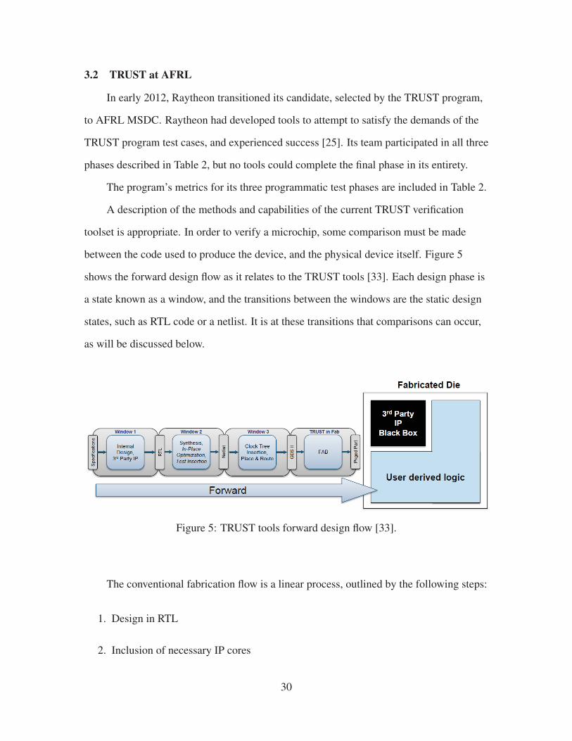
3.2 TRUST at AFRL
In early 2012, Raytheon transitioned its candidate, selected by the TRUST program,
to AFRL MSDC. Raytheon had developed tools to attempt to satisfy the demands of the
TRUST program test cases, and experienced success [25]. Its team participated in all three
phases described in Table 2, but no tools could complete the final phase in its entirety.
The program’s metrics for its three programmatic test phases are included in Table 2.
A description of the methods and capabilities of the current TRUST verification
toolset is appropriate. In order to verify a microchip, some comparison must be made
between the code used to produce the device, and the physical device itself. Figure 5
shows the forward design flow as it relates to the TRUST tools [33]. Each design phase is
a state known as a window, and the transitions between the windows are the static design
states, such as RTL code or a netlist. It is at these transitions that comparisons can occur,
as will be discussed below.
Figure 5: TRUST tools forward design flow [33].
The conventional fabrication flow is a linear process, outlined by the following steps:
1. Design in RTL
2. Inclusion of necessary IP cores
30

3. Device synthesis and optimization
4. Test insertion
5. Clock insertion
6. Place and route
7. Mask generation
8. Fabrication
9. Functional testing
10. System integration
The EDA standard design methodology for ASICs is shown in Figure 6. This design
methodology allows for clear break points in the design process as one moves from
derivation of specifications to final implementation and fabrication. To reverse the
methodology, the physical chipset must be delayered, capturing the metallization and
associated connections before generating an electronic equivalent representation (netlist)
[24]. Once delayering has been performed, the TRUST tools allow the forward data
(golden) to be compared with the reverse data for potential modifications and
identification [33].
31

Figure 6: Standard and reverse EDA design methodologies (Adapted from [25]).
3.3 Test Methodology
Performance is quantified by means of mathematical variables PD, the probability of
correctly identifying extraneous structures, and PFA, the probability of misidentifying a
benign transistor as extraneous. Two levels of testing, which are differentiated using these
variables, are available to identify a chip as being illicitly modified:
Functional testing can verify that a device fails to produce a correct output, but cannot
locate the insertion that causes the error. Functional testing has PD=1 in cases where
an insertion causes an output error, which is excellent for identifying chips that are
not operational. However, PFA for functional testing is unacceptably large for
purposes of locating the extraneous logic. Furthermore, it is important to note that
functional testing will not necessarily identify inserted logic in a circuit, when the
insertion does not modify the current output of the device. In other problem cases,
in which output is not modified under the test conditions (for instance, consider a
series of latches that only modify output after the millionth clock cycle), functional
testing will not identify the malicious insertion or modification. Functional testing
has the benefit of, at the system level, being a non-destructive, non-invasive test [2].
32

Transistor-level testing improves on the ability to locate the insertions, but may sacrifice
the 100% detection rate that functional testing exhibits for circuit modifications that
alter the final output. However, it is also capable of identifying latent, extraneous
transistors that do not necessarily modify the current output of the circuit.
Transistor-level testing is the emphasis of the TRUST program [5].
The TRUST software uses a derivative technique known as gate-level testing.
Gate-level testing takes into account the standard cells used in an intellectual property
library, identifying instances of the cells and examining the resulting logical structures.
For example, a 4-transistor logical NOR gate (that is, the inverse of a logical OR gate) is
likely to be instantiated multiple times in a single design. Modern design methodology
calls for the design of a standard NOR cell, and the instantiation of this cell across the
chip. Leveraging this methodology, the exact pattern of 4 transistors used to generate the
NOR cell is easily recognized by automated tools in the Cell Recognition phase described
in section 3.3.1. Instead of matching 4 transistors, the software needs only match the NOR
cell pattern. Furthermore, more in-depth logical analysis can be performed using the
known output pattern of - in this case - the logical NOR gate. This vastly reduces the
computation requirements, since basic logical operators and even complex structures, like
adders, can be summarized as standard cells.
Functional testing is not sufficient for system integration to occur in defense
microelectronic systems. Therefore, the process must be verified at a lower level by
working backward through the linear steps until initial design elements can be compared
directly against physically fabricated components. Reversal steps are available for nearly
every stage, but not all are viable for device comparison [24].
Reverse fabrication is a process known as delayering. Delayering can be
accomplished by chemical-mechanical polishing (CMP) or via a focused ion beam (FIB)
process. CMP is a coarse grinding process that removes most material indiscriminately,
33
but is not effective for certain metal interconnect layers. FIB offers finer granularity, but is
a slow and expensive process. A method involving stages of each delayering method,
known as hybrid delayering, allows a technician to capture images of the device and
regenerate the mask (that is, the GDSII file) for each layer [25].
The masks represent the first opportunity for comparison; given RTL, the forward
design process can be followed until the mask files are generated, and the results
compared to the actual mask files. Unfortunately, due to inconsistencies between routing
algorithms, and necessary rounding and approximation in the non-deterministic
polynomial-time (NP)-hard problem of VLSI routing, these mask files cannot be expected
to be physically identical, despite that they may be functionally identical [33].
Furthermore, device-level comparison between non-identical masks is intractable without
descending to an earlier stage in the design flow.
The mask files are not the end of the reverse-direction flow, though. Processing the
materials through a device recognition algorithm allows transistors to be recognized, and a
picture of the existing components on the chip to be created. This picture is, in fact, a
textual listing of devices and their interconnection known as a netlist.
Netlists are an intermediate step prior to mask generation in the forward direction,
and are useful for circuit analysis because they list the raw device interconnections.
However, their format poses a challenge in the reverse direction because they lack
human-readable node and wire names. Given that the algorithm producing the netlist was
different for each direction, the forward and reverse netlists are not physically identical
even when they may be functionally identical. However, unlike with mask files, it is
possible to generate a matching between the unnamed nodes of the untrusted
(reverse-generated) netlist and the named nodes of the trusted, golden netlist generated in
the forward direction [24].
34
It is at this level that the TRUST toolset performs its comparisons. In an iterative
process, node group matchings are made based on various factors, and those matchings
are used to infer further matchings. Ideally, a finite number of iterations will yield an exact
matching between golden nodes and untrusted nodes, indicating a circuit that is precisely
to specification. In the event that complete matching is not possible, the extraneous or
omitted logic can be clearly identified, and its function (or lack thereof) deduced. Each
stage in the process is a fundamental building block to the overall algorithmic process, and
will be discussed in detail.
The tools used by the various design stages are listed for reference in Table 3.
A survey of complex digital designs in the public domain will yield a representative
sample of real-world designs. These designs, with varying functionality, will be
synthesized using the Cadence Encounter suite to generate a unique set of test cases that
will stress the TRUST software in both transistor count and standard cell usage. The
equipment required for this experimental investigation is available in the current
laboratory area assigned to this research at MSDC and AFIT, and includes Linux and
Windows workstations with sufficient hardware to execute the software package on
complex test cases as well as run Cadence design tools. The IP for these designs will be
leveraged from preexisting public domain cores or licensed to AFRL or AFIT for
implementation.
In the interest of cost and rapid prototyping, windows of trust concerning trust in
fabrication (TiF) will be omitted from the scope of this research. The forward design
process will be followed as far as layout generation, and netlists will be generated at this
stage. Assuming a flawless delayering and feature extraction process, this is a valid
academic approach to netlist verification.
This experimentation will allow the capabilities of the TRUST software to be
challenged. This software is described in Figure 7 and explained in the following section.
35

Table 3: Tools used in TRUST.
TID Tool Application Source Window
Cell Recognition R3Logic SCR Custom N2G, HIP
R3Logic ULR Custom
Raytheon XOR Scripts
Enhanced DRC Cadence Assura DRC None N2G, HIP
Raytheon eDRC Scripts
Cadence Assura LVS None
Timing Check Cadence Virtuoso None N2G, HIP
Cadence Assura LVS None N2G, HIP
Cadence QRCX None N2G, HIP
Cadence Spectre None HIP
Cadence ELC None HIP
Synopsys Primetime None R2N, N2G, HIP
Encounter Cadence None R2N, N2G, HIP
Hierarchical Extraction Raytheon TSDB Custom N2G, HIP
Equivalence Check Cadence Conformal None R2N, N2G, HIP
Calypto SLEC Enhanced
Calypto Mult Verification Utility Custom
Springsoft Verdi None
Exploitable Logic Check Cadence Conformal Enhanced R2N, N2G, HIP
Springsoft Verdi None
36

Figure 7: Netlist matching toolflow.
3.3.1 Cell Recognition.
When images are taken of a delayered chip, software generates a flattened layout.
This layout does not contain information about the devices in it, only the arrangement of
metal and oxide. The cell recognition step attempts to identify these devices using two
methods.
First, standard cell recognition (SCR) searches for design structures used on the chip
when the library used to generate the devices on the chip is known. This is only applicable
for IP or semi-custom design. If the library is not known, but the design is not fully
custom (as it is likely to be, since fully custom design is often prohibitively laborious), a
process known as unknown library recognition (ULR) is performed to identify the chip’s
standard cell library. Once the library is correctly identified, the SCR step can be
performed on the previously unknown cells.
Not all components will necessarily be identified using library matching, as in
semi-custom design. Those that are will be grouped together with a generated naming
scheme in the output; those that are not will be flagged for future review.
37
The output of the cell recognition step is a gate-level netlist with generically named
nodes, as well as a structured (i.e. not flattened) layout file showing the hierarchy of
component cells. The layout file can aid in identifying unnamed, ungrouped nodes by
function in the netlist later in the process.
3.3.2 Enhanced Design Rule Check.
In the forward design flow, design rule checking is used to verify that rules regarding
device sizing and spacing are enforced. Since most tools seek to size devices to the
minimum area or in multiples of the minimum device size for the technology, any
variations on this modularity may be evidence of hand editing. Such instances are flagged
as highly suspicious, and in later passes may be expected to differ from the golden design.
3.3.3 Timing Check.
Pure logical operation isn’t the only function of a circuit. Real-world circuits are also
subject to timing constraints. Failure to meet these specifications can cause unintended
operation of the circuit. Often, the failure mode for a timing issue in a production system
is a complete system failure; the alternative is an erroneous computed value being
forwarded to other subsystems, which can result in unintended operation. This
vulnerability makes timing a prime target for hardware trojans. To combat the
vulnerability, and detect malicious modifications to the timing configuration of the device,
TRUST tools recreate the parasitic delay model used to plan for timing in the forward
design process, characterize the device and back-annotate the calculated values. Static
timing analysis can then yield results for worst-case timing scenarios, fanout violations
and improperly gated clocks.
The TRUST tools check both interconnect delay and the delay of cells in the device,
each of which provides a parasitic or gate capacitance. Furthermore, entire structures in
the netlist can add stage delay that can indicate additional stage insertion - the tool checks
for these, too.
38

3.3.4 Hierarchical Extraction / TRUST Structural Database.
Hierarchical extraction attempts to realize when a group of library cells forms a
known device, such as an adder. It is primarily utilized when identifying the function of
hard intellectual property (HIP), but is also useful for open library designs. This capability
is valuable, since identifying the purpose of a structure often makes it clear to the tool and
the operator what device is represented from the RTL. It makes finding correct matchings
much simpler since, rather than matching transistors or logic gates, matching is now
performed among complex devices like adders and multiplexers. Figure 8 provides an
overview of the hierarchical functional extraction flow; This window is where the majority
of matching has been performed in test cases [24].
The designs found by survey of commercial and custom libraries are expected to
meet with high PFA in the feature extraction process initially, which is assessed in an
iterative process, shown in Figure 8. The open-source designs do not initially contain
malicious insertions. Therefore, the initial test metric will be PFA and will seek to be
minimized. A low PFA will indicate successful verification of a non-malicious circuit.
The TRUST structural database (TSDB) is a Python tool for analyzing the mapping
process. It is the tool that allows for iterative mapping and engineering inputs
(human-guided matching). TSDB can perform specific matching analyses. Of particular
utility is the ability to analyze location, inputs and outputs of common D flip-flops in the
design to predict which devices between golden and untrusted netlists share the same
configuration and, therefore, may represent the same functional device.
39
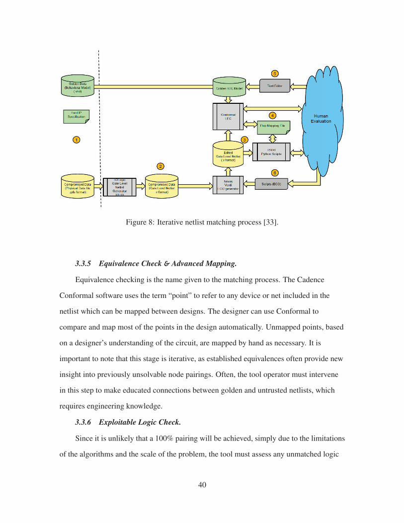
Figure 8: Iterative netlist matching process [33].
3.3.5 Equivalence Check & Advanced Mapping.
Equivalence checking is the name given to the matching process. The Cadence
Conformal software uses the term “point” to refer to any device or net included in the
netlist which can be mapped between designs. The designer can use Conformal to
compare and map most of the points in the design automatically. Unmapped points, based
on a designer’s understanding of the circuit, are mapped by hand as necessary. It is
important to note that this stage is iterative, as established equivalences often provide new
insight into previously unsolvable node pairings. Often, the tool operator must intervene
in this step to make educated connections between golden and untrusted netlists, which
requires engineering knowledge.
3.3.6 Exploitable Logic Check.
Since it is unlikely that a 100% pairing will be achieved, simply due to the limitations
of the algorithms and the scale of the problem, the tool must assess any unmatched logic
40

for likelihood of being malicious. Logic that is found to be unreachable, duplicated (in
series or parallel) or superfluous (i.e. generates a constant) is particularly suspicious, and
may be evidence of tampering. These conditions are each considered by the algorithms
used in the enhanced version of Cadence Conformal used for TRUST.
3.3.7 Conformal for Custom Layouts.
3.3.7.1 Transistor-Level.
To achieve preliminary results, a simple circuit is used to generate two netlists.
Netlists are compared using Cadence Design Systems and Raytheon software. In selecting
the simple circuit to use for proof-of-concept, multiple factors were considered. The
design should not be large or complex, since complications stemming from process failure
should not preclude verification of fundamental operation. Furthermore, the design should
be scalable, such that a somewhat more complex design can be generated rapidly.
To this end, the first article used as proof-of-concept is a single bit full-adder cell of a
ripple-carry adder, for which custom layout has been accomplished in AMI 0.6 μm
technology suitable for fabrication through the Metal Oxide Semiconductor
Implementation Service (MOSIS). Transistor models from the North Carolina State
University (NCSU) process design kit (PDK) are used in the design. The design will be
referred to as “Circuit A”. Results will consist of the novel process used to verify the
circuit.
3.3.7.2 Gate-Level.
The TRUST software is not designed for use with transistor-level verification, but
instead is driven toward verifying circuits at the gate level. In the conventional design
process, each gate is represented by an IP core in a standard logic library. These cells are
combined in different ways to achieve the design objective. As with transistor-level
testing, circuits selected for gate-level testing will seek to explore the capabilities of the
TRUST software in verifying designs outside of the test article suite. Three circuits were
41
selected for testing. Circuit B is a clocked inverter for proof-of-concept. Circuit C is a
fundamental implementation of a “real-world” design, an Inter-Integrated Circuit (I2C)
bus communication core. Circuit D is a full adder of a gate-based architecture, unlike
Circuit A; it is the primary demonstration circuit for the netlist generation and verification
process. Circuit E is an Advanced Encryption Standard (AES) cryptography core chosen
to highlight the complexity of scaling the verification process.
42
IV. Results
This chapter presents the results of applying the methodology described in Chapter 3
to test articles. Subsections present the various experiments in order of complexity, and
sub-subsections present findings. Descriptions are included of lessons learned, and
techniques developed to cope with novel problems. Results, besides demonstrating the
feasibility of verification on real circuits using commercial EDA software, present a
defined process which can be carried on to further work.
4.1 Transistor-level Testing
4.1.1 Preliminary Results with Circuit A.
4.1.1.1 Generation.
Circuit A was presented in subsection 3.3.7. As a review, Circuit A is the first article
used as proof-of-concept. It is a single bit full-adder cell of a ripple-carry adder, for which
custom layout has been accomplished by the author in AMI 0.6 μm technology suitable
for fabrication through MOSIS.
Two netlists are needed for comparison: the golden netlist is derived from the
Virtuoso schematic, using NC-Verilog for Simulation; the revised netlist is extracted from
the custom layout using Virtuoso’s included circuit extraction software and netlisted in
Verilog using NC-Verilog. These two Verilog netlists are eligible inputs for sample
comparison; this process is summarized in Figure 9, and the layout, schematic and their
netlists are shown for visual comparison in Figures 10, 11 and 12.
43

Figure 9: Conceptual process for preliminary results.
Figure 10: Circuit A layout.
44
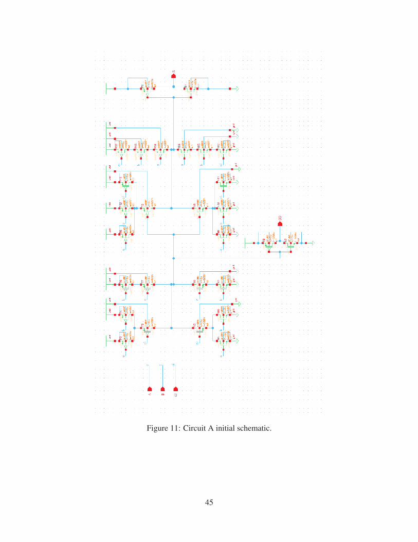
Figure 11: Circuit A initial schematic.
45

Figure 12: Comparison of initial Circuit A layout (left) and schematic (right) netlists as
generated by Cadence software.
46
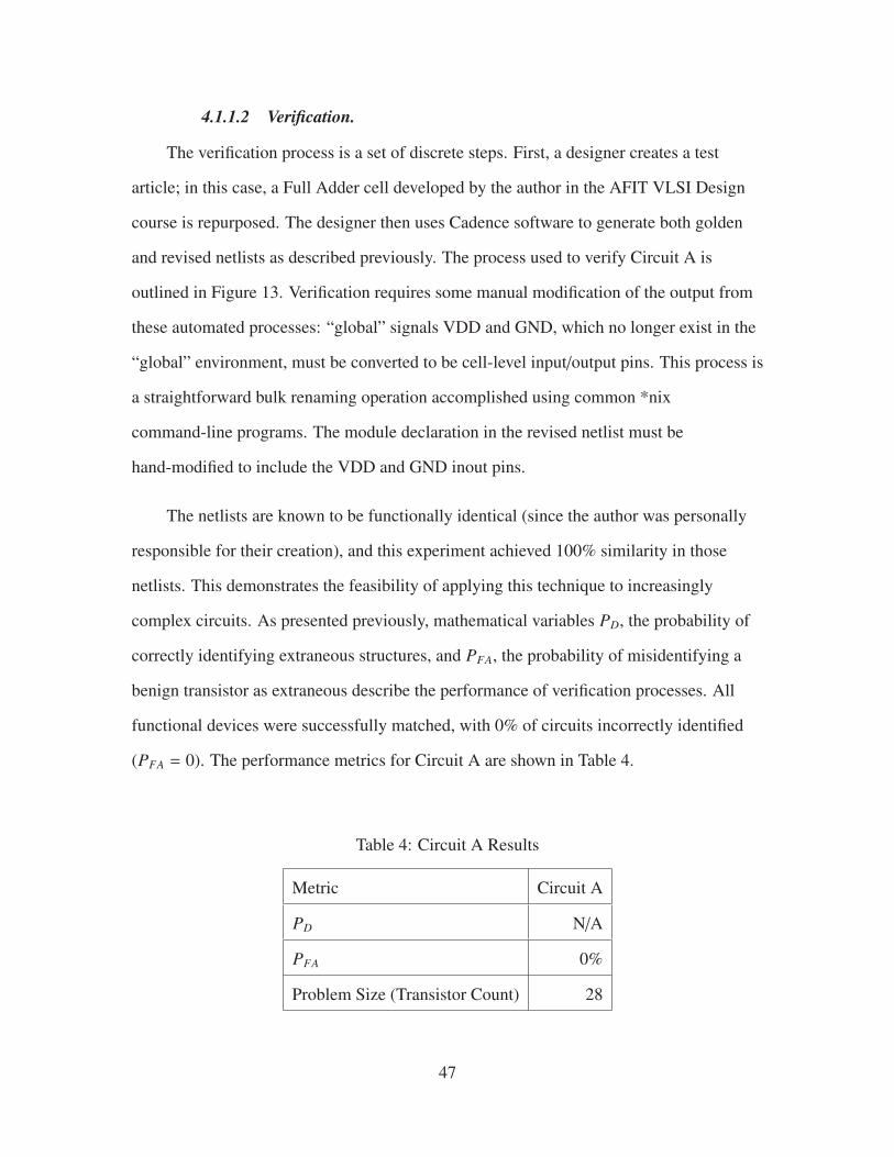
4.1.1.2 Verification.
The verification process is a set of discrete steps. First, a designer creates a test
article; in this case, a Full Adder cell developed by the author in the AFIT VLSI Design
course is repurposed. The designer then uses Cadence software to generate both golden
and revised netlists as described previously. The process used to verify Circuit A is
outlined in Figure 13. Verification requires some manual modification of the output from
these automated processes: “global” signals VDD and GND, which no longer exist in the
“global” environment, must be converted to be cell-level input/output pins. This process is
a straightforward bulk renaming operation accomplished using common *nix
command-line programs. The module declaration in the revised netlist must be
hand-modified to include the VDD and GND inout pins.
The netlists are known to be functionally identical (since the author was personally
responsible for their creation), and this experiment achieved 100% similarity in those
netlists. This demonstrates the feasibility of applying this technique to increasingly
complex circuits. As presented previously, mathematical variables PD, the probability of
correctly identifying extraneous structures, and PFA, the probability of misidentifying a
benign transistor as extraneous describe the performance of verification processes. All
functional devices were successfully matched, with 0% of circuits incorrectly identified
(PFA = 0). The performance metrics for Circuit A are shown in Table 4.
Table 4: Circuit A Results
Metric Circuit A
PD N/A
PFA 0%
Problem Size (Transistor Count) 28
47

Figure 13: Processing Circuit A for Verification.
48

PD, as expected, is irrelevant due to the same reasons previously described: there are
no extraneous insertions present, and so none can be detected. The process did not
successfully verify some points in the circuit that are labeled with “CUT” or “Z”. These
unmapped points are identified as by-products of the initial logic optimization that
Conformal executes. Some examples of these points are shown in Figure 14.
Figure 14: VDD, GND and Z points unmapped by Cadence Conformal.
Hand-correction is possible through user mapping and renaming rules. These
hand-correction steps have met with some, though not complete, success. Because they
are not immediately related to the circuit’s logic, further experimentation is beyond the
scope of the thesis. This iterative mechanism for verifying circuits is essential to
understanding the tool flow.
In order to test the other significant verification metric, PD, extraneous logic must be
inserted in an open-source circuit. Although this may be pursued in future work, it is
outside the scope of this research. It is understood that the two metrics represent a tradeoff
in the verification process, controllable by parameterization of the tool flow.
Runtime, unlike in Table 2, is not noted in Table 4. As the first trial in the
experimentation process, runtime was so small as to be unmeasurable for Circuit A on the
Intel Xeon-powered workstation. The configuration runtime for the engineer himself time
49
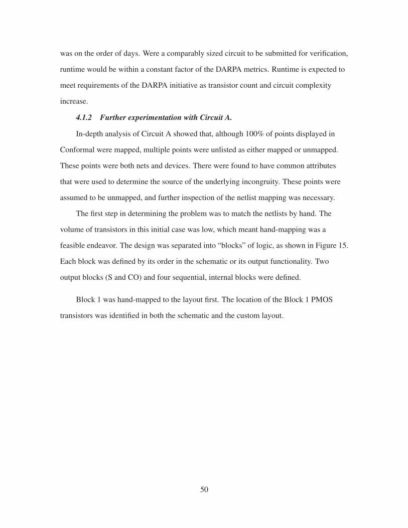
was on the order of days. Were a comparably sized circuit to be submitted for verification,
runtime would be within a constant factor of the DARPA metrics. Runtime is expected to
meet requirements of the DARPA initiative as transistor count and circuit complexity
increase.
4.1.2 Further experimentation with Circuit A.
In-depth analysis of Circuit A showed that, although 100% of points displayed in
Conformal were mapped, multiple points were unlisted as either mapped or unmapped.
These points were both nets and devices. There were found to have common attributes
that were used to determine the source of the underlying incongruity. These points were
assumed to be unmapped, and further inspection of the netlist mapping was necessary.
The first step in determining the problem was to match the netlists by hand. The
volume of transistors in this initial case was low, which meant hand-mapping was a
feasible endeavor. The design was separated into “blocks” of logic, as shown in Figure 15.
Each block was defined by its order in the schematic or its output functionality. Two
output blocks (S and CO) and four sequential, internal blocks were defined.
Block 1 was hand-mapped to the layout first. The location of the Block 1 PMOS
transistors was identified in both the schematic and the custom layout.
50

Figure 15: Circuit A logical blocks
4.1.2.1 Serial ordering.
It was immediately noticed that the functionality was identical, but the ordering of
devices in series was different. In the schematic, the block 1 parallel PMOS transistors
appear to the outside of the carry-in transistor, as shown in Figure 16a. In the layout
(Figure 17), the parallel transistors are inside of the carry-in transistor. The timing of these
two circuits will be slightly different, and so despite their logical equivalence, they do not
map. The Circuit A schematic was corrected here, in both the PMOS and NMOS
transistors, and also in Block 4. The correction applied to Block 1 is shown in Figure 16b.
Note the difference in device numbering. The P5 transistor in Figure 16a is moved to
the outside, and renumbered P17. This is a by-product of the Cadence Virtuoso schematic
editor checking process. It does not follow the same path across the circuit when devices
are rearranged, and so the numbering changes here and elsewhere.
51
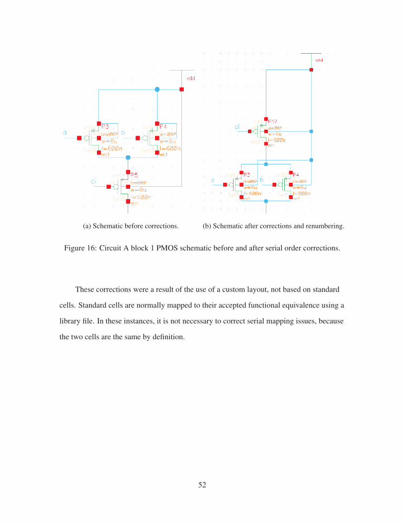
(a) Schematic before corrections. (b) Schematic after corrections and renumbering.
Figure 16: Circuit A block 1 PMOS schematic before and after serial order corrections.
These corrections were a result of the use of a custom layout, not based on standard
cells. Standard cells are normally mapped to their accepted functional equivalence using a
library file. In these instances, it is not necessary to correct serial mapping issues, because
the two cells are the same by definition.
52
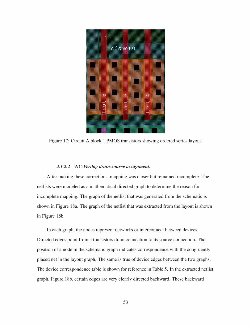
Figure 17: Circuit A block 1 PMOS transistors showing ordered series layout.
4.1.2.2 NC-Verilog drain-source assignment.
After making these corrections, mapping was closer but remained incomplete. The
netlists were modeled as a mathematical directed graph to determine the reason for
incomplete mapping. The graph of the netlist that was generated from the schematic is
shown in Figure 18a. The graph of the netlist that was extracted from the layout is shown
in Figure 18b.
In each graph, the nodes represent networks or interconnect between devices.
Directed edges point from a transistors drain connection to its source connection. The
position of a node in the schematic graph indicates correspondence with the congruently
placed net in the layout graph. The same is true of device edges between the two graphs.
The device correspondence table is shown for reference in Table 5. In the extracted netlist
graph, Figure 18b, certain edges are very clearly directed backward. These backward
53

edges are highlighted in red. A backward edge indicates that the netlist has listed the
actual drain as the source, and the actual source as the drain. Inspection of the netlist
verified this observation.
This observation prompts investigation into its cause. Comparing the layout of the
devices which netlisted correctly (Inst 4, 6, 7, 11, 20, 19, 26, 39, 23, 25, 30, 22 and 38)
with those which netlisted incorrectly (Inst 17, 5, 9, 14, 16, 15, 3, 13, 24, 28, 33, 36, 35,
34 and 32) showed a key difference. The correct devices had the source connections on
the left side, as viewed from the top in layout view. The incorrect devices had the drain on
the left, and the source on the right.
An example of such a backward device from block 4 is shown in the following
figures. The block 4 PMOS schematic is shown in Figure 19.
In the schematic, NC-Verilog follows the device labels to determine the source and
drain connections. However, the layout has no device labels, and they must be implied, as
shown by the block 4 PMOS layout in Figure 20.
Since NC-Verilog has no knowledge of the “correct” direction of carrier flow through
the channel in a transistor, it is unable to make an educated assumption about the drain
and source. Instead, it always labels the leftmost connection as the source, and the
rightmost as the drain. In complementary metal-oxide semiconductor (CMOS) devices
that output from their drain on the left, this is the incorrect guess. Figure 20 has its true
source on the right, and its drain on the left.
In simulation, this will make no difference as the transistor models are effectively
bidirectional. Thus, the tool - “NC-Verilog for Simulation” - does not expend effort in
assigning the correct direction. To correct the incorrect terminal assignments, transistors
running right-to-left were identified, and their assignments in the netlist swapped. This
correction is shown in Figure 21.
54

Table 5: Circuit A device correspondence
Block FET Type Extracted Schematic
1 PMOS Inst 11 P18
Inst 14 P19
Inst 16 P20
NMOS Inst 30 N21
Inst 33 N22
Inst 35 N23
2 PMOS Inst 19 P7
Inst 20 P6
NMOS Inst 38 N6
Inst 39 N7
3 PMOS Inst 4 P8
Inst 5 P10
Inst 6 P11
Inst 3 P9
NMOS Inst 23 N9
Inst 24 N10
Inst 25 N11
Inst 22 N8
4 PMOS Inst 9 P12
Inst 13 P13
Inst 15 P14
NMOS Inst 28 N12
Inst 32 N13
Inst 34 N14
S PMOS Inst 17 P1
NMOS Inst 36 N1
CO PMOS Inst 7 P0
NMOS Inst 26 N0
55

(a) Schematic netlist graph with legend.
(b) Extracted netlist graph with legend. Red highlights transistors with backward assignments.
Figure 18: Circuit A netlist directed graphs, with legend
56

Figure 19: Left-to-Right Schematic.
Figure 20: Left-to-Right Layout.
57

Figure 21: Representative Left-to-Right Netlist Modification. Green indicates drains
changed to sources; Red indicates the opposite.
58
4.2 Gate-level Testing
As discussed in Section 3.3.7.2, gate-level testing is the focus of the TRUST tools as
they are designed. This section presents testing for Circuits B, C and D is described in this
section, and discusses results.
4.2.1 Circuit B.
Before a complex circuit could be assessed, a simple one was used to develop the
workflow and configure the environment. For this proof-of-concept, a clocked inverter
was chosen.
4.2.1.1 Generation.
The inverter, referred to as “Circuit B”, was first composed in Very-High-Speed
Integrated Circuit Hardware Description Language (VHDL), as shown in Figure 22.
1 library IEEE;2 use IEEE.STD_LOGIC_1164.ALL;3 use IEEE.STD_LOGIC_ARITH.ALL;4 use IEEE.STD_LOGIC_UNSIGNED.ALL;5
6 entity INV1 is7 port ( A: in STD_LOGIC;8 clk: in STD_LOGIC;9 B: out STD_LOGIC);
10 end INV1;11
12 architecture BEHAVIORAL of INV1 is13 begin14 clkproc: process (clk)15 begin16 if(rising_edge(clk)) then17 B <= NOT A;18 end if;19 end process;20 end BEHAVIORAL;
Figure 22: Circuit B VHDL code.
59

The VHDL was compiled into a Verilog netlist using standard cells with Cadence
RTL Compiler (rc). RTL Compiler requires a Tool Command Language (Tcl) script to
operate. The script used for Circuit B is shown in Figure 23.
From this stage forward, all work is completed using standard cells in the IBM 90 nm
9SF “6 02 00” technology, suitable for fabrication through the Trusted Foundry program.
The resulting design, represented as a Verilog netlist of standard cells in the 9SF
technology, was composed of one D flip-flop cell, for latching of the clock, and one
inverter cell from the standard cell library.
Encounter import is accomplished by importing the RTL twice: once as a design, and
then separately as RTL. This allows the appropriate timing libraries to be included; as
timing is not optimized for these test cases, the “typical”, rather than maximum and
minimum, library is sufficient. The Verilog netlist is shown in Figure 24.
The smallest-area cells were used, and as a result the design was simulated to
experience 1.178 nsec of average delay input-to-output, and dissipate a total of
103.086 nW. A schematic created by Cadence Conformal is shown in Figure 25, which
was verified in netlist form using Assura LVS.
Assura LVS required Extract and Compare rules as well as binding files as provided
by the IBM PDK. The Assura LVS GUI is shown configured as described in Figure 26.
60

1 set_attribute library {lp_typ_12.lib}2 set_attribute hdl_vhdl_environment {common}
3
4 set myPeriod_ps 1000000;# Clock period in ps5 set myInDelay_ns 1000;# delay from clock to inputs valid6 set myOutDelay_ns 1000;# delay from clock to output valid7
8 # Analyze and Elaborate the HDL files
9 read_hdl -vhdl inv_top.vhd
10 elaborate INV1
11
12 # Apply Constraints and generate clocks
13 set clock [define_clock -period ${myPeriod_ps} -name clk [←↩clock_ports]]
14 external_delay -input $myInDelay_ns -clock clk [find / ←↩-port ports_in/*]
15 external_delay -output $myOutDelay_ns -clock clk [find / ←↩-port ports_out/*]
16
17 # Sets transition to fall/rise 400ps
18 dc::set_clock_transition .4 clk
19
20 # check that the design is OK so far
21 check_design -unresolved
22 report timing -lint
23
24 # Synthesize the design to the target library
25 synthesize -to_mapped
26
27 # Write out the reports
28 report timing > INV1_timing.rep
29 report gates > INV1_cell.rep
30 report power > INV1_power.rep
31
32 # Write out the structural Verilog and sdc files
33 write_hdl -mapped > inv1-out.v
34 write_sdc > inv1-out.sdc
Figure 23: Circuit B RTL Compiler TCL script.
61

1 module INV1(A, clk, B);2 input A, clk;3 output B;4 wire A, clk;5 wire B;6 wire n_0;7 dff_1x B_reg(.clk (clk), .d (n_0), .q (B));
8 inv_1x g4(.in0 (A), .y (n_0));
9 endmodule
Figure 24: Circuit B Verilog code.
Figure 25: A symbolic schematic of Circuit B, the clocked inverter.
Figure 26: The Assura LVS GUI, configured to incrementally verify Circuit B.
62

4.2.1.2 Verification.
The Verilog netlist is used as an input, much as the netlists derived from Virtuoso
schematics and layouts were. A second netlist was generated for comparison by
completing place-and-route on the clocked inverter. Cadence Encounter took the netlist as
input and generated a floorplan of the cells as they might be laid out on-die. From this
layout, another netlist was generated for use as an input. It was found that the embedded
tool chain in Cadence Encounter used an RTL Compiler implementation similar to the
standalone software. Due to this similarity, the revised netlist and the golden netlist were
nearly identical, to include the naming of points. Sending these netlists and their
corresponding libraries to Cadence Conformal resulted in 100% matching of points. This
is shown in Figure 27.
Figure 27: Conformal showing mapped points in Circuit B.
This result, however trivial, is an important step in verifying the circuit in the current
tool flow. It demonstrates that netlists from this process are capable of being matched at
the fundamental level. The process is summarized in a flowchart, seen in Figure 28.
Further experiments will seek to increase the complexity of the circuit, as well as
seek greater separation between the RTL from which the golden netlist is generated and
the TRUST window in which the revised netlist is generated.
63
TRUST Library Verification(Conformal)
Place and Route(Encounter)
Golden Generation(rc)
Create Test Article
RTL Compiler(rc)
GoldenNetlist(Verilog)
IBM 90nm 9SF“6_02_00”
Standard Cells
Tcl Script
EncounterPlace & Route
TimingLibrary (typ)
RevisedNetlist(Verilog)
Mapped
(Green)
Renaming Rules &Manual Mapping
Setup Commands
Unmapped
(Yellow)
Extra
(Yellow)
LogicalEquivalenceCheck (LEC)
SuccessfulVerification
Unreachable
(Red)
InitializeConformal
Do file
Figure 28: Processing Circuit B for Verification.
64
4.2.2 Circuit C.
Circuit C is an implementation of the I2C bus communication protocol. Its purpose is
to take the fundamental process demonstrated in Circuit B and apply it to a design sourced
from public repositories. Furthermore, Circuit C was designed to demonstrate that
techniques proven on Circuit B remain valid when scaled in complexity. Behavioral
VHDL was sourced from OpenCores, a website that provides RTL designs that are
community-designed and tested. The project is licensed under the open GPL license [17].
The same process as noted in Figure 28 was used. A significant difference is that the
design has three modules (i2c master top, byte ctrl and bit ctrl), arranged hierarchically.
The software handled this difference without any changes to the configuration, resolving
the hierarchy as appropriate. Golden generation was accomplished using Cadence RTL
Compiler, and a nearly-identical Tcl configuration script. No settings were changed but
the module names, to include top-level timing. The resulting netlist used 645 cells of 35
unique types; input-to-output delay was estimated at 1.636 ns. The top-level
(i2c master top) schematic is shown in Figure 29. Sub-modules are represented by black
boxes.
The structural Verilog netlist was considered golden. Place and route were
completed, and a revised netlist generated, precisely as with Circuit B. Cadence
Conformal matched the netlists exactly. As discussed in the previous section, this is
expected due to Encounter’s backend being the same as the RTL Compiler frontend. The
significant contribution of Circuit C is the generation of a test article from a novel source,
using an intermediate number of unique and total standard cells. Additionally, Circuit C
shows that Circuit B processes do not need modification as the reference design is scaled
to greater complexity.
65

Figure 29: A symbolic schematic of Circuit C at the top level.
4.2.3 Circuit D.
The next stage of test article design was chosen on multiple criteria. First, it was to
demonstrate greater complexity than Circuit B, though not necessarily as complex as
Circuit C. Second, it should provide the opportunity to use more verification tools from
the TRUST software set. This second goal increases the process complexity, which
necessitates the decrease in design complexity.
4.2.3.1 Generation.
To attain these attain these goals, the following novel method is proposed. First, a
hardware description language (HDL) representation of a generic full adder was
repurposed from a reference design. This HDL is shown in Figure 30.
Then, Cadence RTL Compiler generates a Verilog netlist based on the HDL design.
The Tcl script used to execute RTL Compiler was nearly identical to that used in Circuit
66
1 LIBRARY ieee;2 USE ieee.std_logic_1164.ALL;3
4 ENTITY FA IS5 PORT(6 a : IN STD_LOGIC;
7 b : IN STD_LOGIC;
8 c_in : IN STD_LOGIC;
9 sum : OUT STD_LOGIC;
10 c_out : OUT STD_LOGIC);
11 END FA;12
13 ARCHITECTURE behv OF FA IS14 BEGIN15 sum <= a XOR b XOR c_in;16 c_out <= (a AND b) OR (c_in AND (a OR b));17 END behv;
Figure 30: VHDL for Circuit D.
B. Since the standard cell library contained a full adder cell already, the initial output of
RTL Compiler was trivial, as shown in Figure 31.
Figure 31: A schematic of the single-cell Circuit Prototype D1.
67
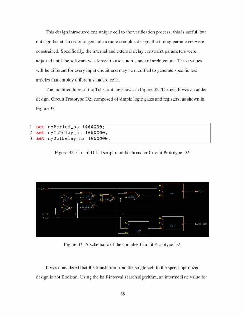
This design introduced one unique cell to the verification process; this is useful, but
not significant. In order to generate a more complex design, the timing parameters were
constrained. Specifically, the internal and external delay constraint parameters were
adjusted until the software was forced to use a non-standard architecture. These values
will be different for every input circuit and may be modified to generate specific test
articles that employ different standard cells.
The modified lines of the Tcl script are shown in Figure 32. The result was an adder
design, Circuit Prototype D2, composed of simple logic gates and registers, as shown in
Figure 33.
1 set myPeriod_ps 1000000;2 set myInDelay_ns 1000000;3 set myOutDelay_ns 1000000;
Figure 32: Circuit D Tcl script modifications for Circuit Prototype D2.
Figure 33: A schematic of the complex Circuit Prototype D2.
It was considered that the translation from the single-cell to the speed-optimized
design is not Boolean. Using the half-interval search algorithm, an intermediate value for
68

timing, shown in Figure 34, was found that produces a semi-optimized test article, Circuit
Prototype D3.
1 set myPeriod_ps 10000002 set myInDelay_ns 4998003 set myOutDelay_ns 499800
Figure 34: Circuit D Tcl script modifications for Circuit Prototype D3.
The resulting design uses three standard cells - more than the single-cell design, but
fewer than the speed-optimized design. The schematic for this version of the design is
shown in Figure 35. Verification was not pursued for this design.
Figure 35: A schematic of Circuit Prototype D3.
4.2.3.2 Verification.
The process used for Circuit B was followed with no modifications to the steps listed
in Section 4.2.1. The successful results of Assura LVS are shown in Figure 36.
69
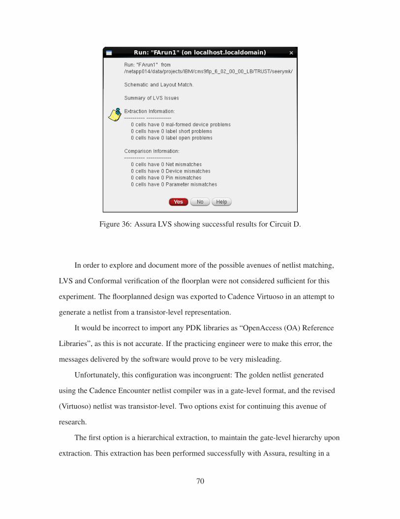
Figure 36: Assura LVS showing successful results for Circuit D.
In order to explore and document more of the possible avenues of netlist matching,
LVS and Conformal verification of the floorplan were not considered sufficient for this
experiment. The floorplanned design was exported to Cadence Virtuoso in an attempt to
generate a netlist from a transistor-level representation.
It would be incorrect to import any PDK libraries as “OpenAccess (OA) Reference
Libraries”, as this is not accurate. If the practicing engineer were to make this error, the
messages delivered by the software would prove to be very misleading.
Unfortunately, this configuration was incongruent: The golden netlist generated
using the Cadence Encounter netlist compiler was in a gate-level format, and the revised
(Virtuoso) netlist was transistor-level. Two options exist for continuing this avenue of
research.
The first option is a hierarchical extraction, to maintain the gate-level hierarchy upon
extraction. This extraction has been performed successfully with Assura, resulting in a
70

gate-level design in the same standard cell library. Special considerations must be made to
facilitate exportation to the Virtuoso environment.
For instance, no power rails or rings should be placed. These structures create
extraneous nets, which do not exist in the HDL and thus will not match. Alternatively,
VDD and VSS/GND nets can be included as I/O pins in the HDL. This is necessary at the
cell level, however, and so would require a supporting standard cell library.
To accomplish this process, the Cadence documentation can be followed with the
following modifications. Skip any steps relating to power ring generation. Skip the
“special route” step that generates power rails and contacts leading to the rings. Add cell
padding greater than the specified values, at a value of at least the maximum overlap of the
widest cell in the design.
Additionally, cell overlap and mirrored placement import is not straightforward in
Virtuoso; for creating the test article, it is simpler to modify the placement parameters.
The configuration and export script used is shown in Figure 37.
The line “floorPlan -flip n -site unit -r 0.460273972603 0.5 0.0
0.0 0.0 0.0” configures the floorplan to leave room for cells that are not mirrored.
Extra cell and line spacing are specified to keep cells from shorting out on each other
where placement is tight. The result is a design that will not be optimized for area, timing
or power; however, it is logically valid. The line “dbSet [dbGet -p2
top.insts.cell.name *].orient R0” manually interfaces with the cell placement
database that underlies the Encounter GUI. It reorients all the cells to “R0” orientation,
the default unmirrored, unflipped orientation. Following reorientation, the placement must
be refined to ensure there are no violations in the new circuit. Finally, routing must be
accomplished to connect the cells’ pins and form the logic circuit.
The second option for continued research, which is in theory closer to the actual
procedure for verifying a factory-produced microchip, is to perform SCR on the circuit.
71
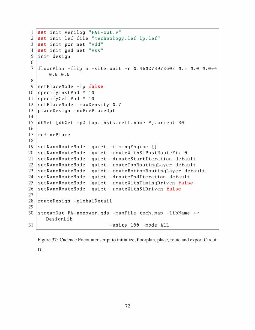
1 set init_verilog "FA1-out.v"2 set init_lef_file "technology.lef lp.lef"3 set init_pwr_net "vdd"4 set init_gnd_net "vss"5 init_design
6
7 floorPlan -flip n -site unit -r 0.460273972603 0.5 0.0 0.0←↩0.0 0.0
8
9 setPlaceMode -fp false10 specifyInstPad * 10
11 specifyCellPad * 10
12 setPlaceMode -maxDensity 0.7
13 placeDesign -noPrePlaceOpt
14
15 dbSet [dbGet -p2 top.insts.cell.name *].orient R0
16
17 refinePlace
18
19 setNanoRouteMode -quiet -timingEngine {}
20 setNanoRouteMode -quiet -routeWithSiPostRouteFix 0
21 setNanoRouteMode -quiet -drouteStartIteration default
22 setNanoRouteMode -quiet -routeTopRoutingLayer default
23 setNanoRouteMode -quiet -routeBottomRoutingLayer default
24 setNanoRouteMode -quiet -drouteEndIteration default
25 setNanoRouteMode -quiet -routeWithTimingDriven false26 setNanoRouteMode -quiet -routeWithSiDriven false27
28 routeDesign -globalDetail
29
30 streamOut FA-nopower.gds -mapFile tech.map -libName ←↩DesignLib
31 -units 100 -mode ALL
Figure 37: Cadence Encounter script to initialize, floorplan, place, route and export Circuit
D.
72
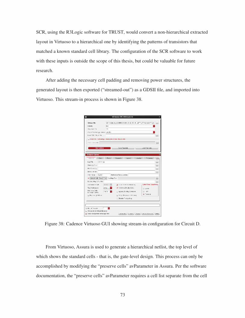
SCR, using the R3Logic software for TRUST, would convert a non-hierarchical extracted
layout in Virtuoso to a hierarchical one by identifying the patterns of transistors that
matched a known standard cell library. The configuration of the SCR software to work
with these inputs is outside the scope of this thesis, but could be valuable for future
research.
After adding the necessary cell padding and removing power structures, the
generated layout is then exported (“streamed-out”) as a GDSII file, and imported into
Virtuoso. This stream-in process is shown in Figure 38.
Figure 38: Cadence Virtuoso GUI showing stream-in configuration for Circuit D.
From Virtuoso, Assura is used to generate a hierarchical netlist, the top level of
which shows the standard cells - that is, the gate-level design. This process can only be
accomplished by modifying the “preserve cells” avParameter in Assura. Per the software
documentation, the “preserve cells” avParameter requires a cell list separate from the cell
73

library in order to identify standard cells. This file can be created from a multitude of
sources; in this case, it was accomplished with a script created specifically for this effort
that extracted the list from the “lp.lef” technology description file.
The design was shown to pass LVS in Encounter, as with Circuit B. However, LVS in
Virtuoso is not feasible since only the layout is exported, not the schematic. Even so,
repeating LVS could be seen as a trivial exercise, and has not been pursued further.
Additionally, LVS was attempted using the method discussed previously, by adding
VDD and VSS pins to the necessary modules. Because the extraction is performed
hierarchically at this stage, it is only necessary to add the declarations (..., .vss
(vss), .vdd (vdd));) to each cell instance in the top-level module. The
“resimulate extracted” switch is necessary when performing Assura LVS.
At this stage, a netlist is also available through the Assura “view netlist” command.
This netlist uses the same naming and wiring as the input netlist, and is easily verified
using Conformal.
4.2.4 Circuit E.
Circuit E is a test article designed using an AES cryptography core chosen to
highlight the complexity of scaling the verification process. The goals for Circuit E are
analogous to those of Circuit C: migrate the previous process to a more complex design,
demonstrating that the procedure remains valid. It incorporates another
community-sourced design from OpenCores, under the Apache license [19]. Circuit E is
also the first attempt at implementing a Verilog HDL base rather than VHDL.
The AES core was coded to work with either a 128, 192 or 256-bit encryption key.
256-bit encryption is certified by National Institute of Standards and Technology (NIST)
to be appropriate for secure defense encyption at the TOP-SECRET level [30], and so is
immediately relevant to the TRUST efforts.
74
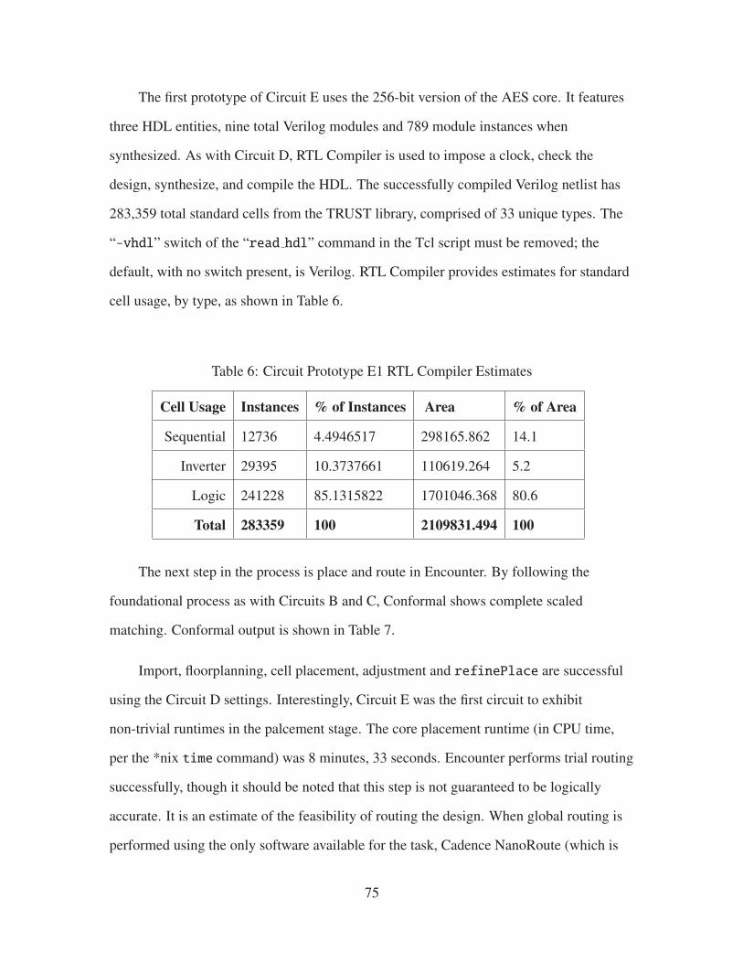
The first prototype of Circuit E uses the 256-bit version of the AES core. It features
three HDL entities, nine total Verilog modules and 789 module instances when
synthesized. As with Circuit D, RTL Compiler is used to impose a clock, check the
design, synthesize, and compile the HDL. The successfully compiled Verilog netlist has
283,359 total standard cells from the TRUST library, comprised of 33 unique types. The
“-vhdl” switch of the “read hdl” command in the Tcl script must be removed; the
default, with no switch present, is Verilog. RTL Compiler provides estimates for standard
cell usage, by type, as shown in Table 6.
Table 6: Circuit Prototype E1 RTL Compiler Estimates
Cell Usage Instances % of Instances Area % of Area
Sequential 12736 4.4946517 298165.862 14.1
Inverter 29395 10.3737661 110619.264 5.2
Logic 241228 85.1315822 1701046.368 80.6
Total 283359 100 2109831.494 100
The next step in the process is place and route in Encounter. By following the
foundational process as with Circuits B and C, Conformal shows complete scaled
matching. Conformal output is shown in Table 7.
Import, floorplanning, cell placement, adjustment and refinePlace are successful
using the Circuit D settings. Interestingly, Circuit E was the first circuit to exhibit
non-trivial runtimes in the palcement stage. The core placement runtime (in CPU time,
per the *nix time command) was 8 minutes, 33 seconds. Encounter performs trial routing
successfully, though it should be noted that this step is not guaranteed to be logically
accurate. It is an estimate of the feasibility of routing the design. When global routing is
performed using the only software available for the task, Cadence NanoRoute (which is
75

Table 7: Circuit Prototype E1 foundational Conformal verification.
Compare Result Golden Revised
Root module name aes 256 aes 256
Primary inputs 385 385
- Mapped 385 385
Primary outputs 128 128
- Mapped 128 128
State key points 12736 12736
- Mapped 12736 12736
part of the Encounter backend), the software hangs on initialization. No cause or
resolution of the NanoRoute problem has been identified.
76

4.3 Summary
Techniques described in Chapter 3 were applied to test articles, and the procedures
and results documented in this chapter. Circuit A’s initial results were presented, and
further experimentation was conducted to solve various novel problems. Descriptions
were provided in hierarchical format of the solution steps to these problems in a way that
could be employed in the mapping of future complex circuits.
Results show both transistor- and gate-level verification processes. These results
demonstrate a spectrum of complexity. Discussion includes both process performance in
scaling as well as verification. The process itself is described in detail, and can be adapted
in whole or in part to other verification applications.
77

V. Conclusion and Future Work
5.1 Summary
This thesis has presented a process for verifying the operation of tools used in the
DARPA TRUST program when applied to test cases outside of those provided by the
program.
At the transistor level, two processes were established. First, a process to generate a
feasible test article was created; second, a means of verifying this test article was
established, and lastly both processes were refined as unique traits of the problem instance
were noted. The end result was an end-to-end process for successfully generating and
verifying a test article.
At the gate level, results show methods to generate test articles complete to two
different entry points in the forward design process. Additionally, techniques for
successfully verifying these test articles are presented.
This research demonstrates the potential of applying software designed for TRUST
test articles on microchips from questionable sources. A specific process is developed for
both transistor-level library cell verification and gate-level circuit verification. The relative
effectiveness and scalability of the process is assessed.
5.2 Future Work
There are further valid approaches for generating input to the TRUST suite. Netlists
can be generated through:
• synthesis of designer-composed VHDL models,
• extraction from a comparable but non-identical custom layout using the same
library cells,
• extraction from a functionally identical schematic, or
78

• hand-modified to obfuscate the naming and ordering of nets.
These approaches may be valuable in targeting capabilities of the toolset for
specialized cases in future work. Future work may focus on applying these techniques to
increasingly complex circuits. The complexity of future circuits will stem from having
many more transistors, more complex organization and suitability for fabrication in the
IBM technologies available through TAPO. Furthermore, experiments may be performed
on chips known to contain extraneous circuits. Analysis of PFA in real-world circuits
containing extraneous insertions will necessitate PD analysis as well.
5.2.1 Circuit A − 1.
Verification of a circuit simpler than Circuit A should be attempted. Circuit A
encountered many unexpected problems unique to the study of custom circuit verification.
Now that these problems are better defined, a circuit may be designed that does not
encounter them. For instance, a simple inverter with only left-to-right transistor routing
and no serial ordering conflicts would show baseline operation of Cadence Conformal.
This even-simpler step could be considered as the precursor in complexity to Circuit A;
thus, “Circuit A − 1”
5.2.2 Circuit A + 1.
The logical extension of Circuit A, a single bit adder cell, is a multiple-bit ripple
carry adder made by repetition of the single cell at the transistor level. This would show
some effects of problem scaling on the verification process. Alternatively, the adder could
be modeled as a standard cell, and the effects of using custom-built standard cells could be
observed.
5.2.3 SCR and Other Netlists.
A novel means of continuing this avenue of research would be performing SCR on a
non-hierarchical Virtuoso layout as a means of generating a test article. This would add
the real-world complexity of a cell without a defined hierarchy; this thesis assumed the
79

SCR process to be complete at the point of testing in all cases. The R3Logic tool in the
TRUST software suite is designed with this end in mind, but has not been proven on test
articles outside of the TRUST cases.
In this same regard, any investigation into further netlist sources to use in the
generation of test cases is a valid continuation of this research. Such test cases may prove
to better represent performance of a real circuit returned from a fabrication facility.
5.2.4 Additional Tools.
There are many software tools in the TRUST suite. Some of them have been
demonstrated in these results; more have yet to be explored. Building on the test article
generation and fundamental verification techniques shown, more TRUST tools can be
incorporated into the test that reach further into the design process, or that verify
particularly “hard” circuits. Eventually, if all the tools could be implemented, a complete
end-to-end verification process would exist.
5.2.5 Circuit Prototype E2 and Further Complexity Scaling (Circuit F).
Testing on Circuit E is incomplete due to a bug in the Cadence software. In order to
work around this bug, it may be fruitful to attempt verification of the 128-bit version of
the AES core, which is certified by NIST to be sufficient for cryptography at the SECRET
level [30]. The 128-bit core, Circuit Prototype E2, has already been successfully
translated to structural Verilog by RTL Compiler. Using similar HDL to Circuit Prototype
E1, it is compiled to only 559 instances. These compose 199,360 total cells of 30 unique
types. This is approximately a 30% reduction in both total cells and area over Circuit
Prototype E1. By area, the design is estimated to be 10.5% sequential structures, 5.5%
inverters and 84.0% logic structures.
Even the most complex experiment in this thesis, Circuit E, is still much less complex
than many real-world circuits. The general increase of complexity to a notional Circuit F
80

is a valid and worthwhile pursuit. Furthermore, there is opportunity for further research in
complexity increase, toward the end of delayering of deployed defense devices.
5.2.6 Fabrication.
The ultimate goal of this research is to verify fabricated circuits. Therefore, the best
test case possible would be a tangible, fabricated IC. This IC would be designed by the
researcher, or could be sourced from real parts. The chip would be actually delayered,
imaged, and recognized. A scenario such as this would test every part of the TRUST suite,
including the components used to verify trust in fabrication.
5.3 Conclusion
The refinement of this process will further automate and guide verification. The
impact of an improved verification process is a decrease in both risk and cost, as well as
improved reliability and trust associated with commercially acquired microelectronics for
defense purposes [11]. Identifying the physical location of malicious logic is important
from an intelligence perspective [13]. Understanding Trojan implementation allows
prediction of future attack vectors [28] and identification of the stage at which the trusted
supply chain may have been compromised [27]. By this means, adaptive, rather than
reactive, solutions to the trust problem can be implemented. Design verification can, as
research techniques are applied practically, be affordable and feasible on a large scale for
the defense mission of the United States of America.
81

Bibliography
[1] Adee, Sally. “The Hunt for the Kill Switch”. IEEE Spectrum, 1 May 2008.
Available:
http://spectrum.ieee.org/semiconductors/design/the-hunt-for-the-kill-switch [Last
accessed: May 2013].
[2] Beaumont, Mark, Bradley Hopkins, and Tristan Newby. Hardware TrojansPrevention, Detection, Countermeasures (A Literature Review). Technical report,
Command, Control, Communications and Intelligence Division, Defence Science
and Technology Organisation, Australian Department of Defence, Jul 2011.
[3] Behrens, Peter. “DoD Accredited Trusted Sources for Microelectronics”, 2010.
National Semiconductor Corporation Trusted Solutions Business Unit.
[4] Chakraborty, R.S., S. Narasimhan, and S. Bhunia. “Hardware Trojan: Threats and
emerging solutions”. High Level Design Validation and Test Workshop, 2009.HLDVT 2009. IEEE International, 166–171. 2009. ISSN 1552-6674.
[5] Collins, Dean. “DARPA “TRUST in IC’s” Effort”, 2007. URL
http://www.dtic.mil/docs/citations/ADA503809. DARPA Microsystems Technology
Symposium.
[6] Committee on Armed Services. Inquiry into Counterfeit Electronic Parts in theDepartment of Defense Supply Chain. Technical report, US Senate, May 2012. URL
http://www.armed-services.senate.gov/Publications/Counterfeit%20Electronic%
20Parts.pdf.
[7] Crawford, Mark H. “Counterfeits and the U.S. Industrial Base”, 2010. URL
http://www.semi.org/cms/groups/public/documents/web content/ctr 038717.pdf.
Semicon West.
[8] Defense Science Board. High Performance Microchip Supply. Technical report,
Office of the Under Secretary of Defense For Acquisition, Technology, and
Logistics, Feb 2005. URL http://www.acq.osd.mil/dsb/reports/ADA435563.pdf.
[9] Department of Commerce. Counterfeit Electronics Survey. Technical report, Office
of Technology Evaluation, Nov 2009.
[10] Department of Commerce. Defense Industrial Base Assessment: CounterfeitElectronics. Technical report, Office of Technology Evaluation Bureau of Industry &
Security, Jan 2010. URL http://www.bis.doc.gov/defenseindustrialbaseprograms/
osies/defmarketresearchrpts/final counterfeit electronics report.pdf.
82

[11] Deputy Secretary of Defense. Defense Trusted Integrated Circuit Strategy. Technical
report, US Department of Defense, Oct 2003. URL
http://www.trustedfoundryprogram.org/industry-resources-d/doc details/
9-dod-memorandum-defense-trusted-integrated-circuit-strategy.
[12] Deputy Secretary of Defense. Supply Chain Risk Management (SCRM) to Improvethe Integrity of Components Used in DoD Systems. Technical report, US Department
of Defense, Mar 2010. URL http://www.fas.org/irp/doddir/dod/dtm-09-016.pdf.
[13] DoD CIO/USD(AT&L). Protection of Mission Critical Functions to Achieve TrustedSystems and Networks (TSN). Technical report, Office of Under Secretary of
Defense for Acquisition, Technology, and Logistics, Nov 2012. URL
http://www.dtic.mil/whs/directives/corres/pdf/520044p.pdf.
[14] Gavrielov, Moshe. “Letter to Senate Committee on Armed Services.” Official
correspondence., 26 Oct 2011. Available:
http://www.levin.senate.gov/download/?id=ab73c089-eeff-493a-ab8a-
5430b34935dc [Last accessed: May
2013].
[15] Glum, Ted. “DoD Microelectronics Strategic Management”, 2005. URL
http://www.pcfse.org/Meetings2005/minutesoct2005/glum.pps. Professional
Council of Federal Scientists and Engineers Meeting.
[16] Grow, Brian, Chi-Chu Tschang, Cliff Edwards, and Brian Burnsed. “Dangerous
Fakes.” BusinessWeek., 1 Oct 2008. Available:
http://www.BusinessWeek.com/stories/2008-10-01/dangerous-fakes [Last accessed:
May 2013].
[17] Herveille, Richard. “I2C controller core”. OpenCores, 25 Apr 2013. URL
http://opencores.org/project,i2c. GPL License. Last accessed Winter 2013.
[18] Houghton, Kimberley. “BAE Systems gets chunk of jet contract”. Union Leader, 5
January 2012. Available:
http://www.unionleader.com/article/20120105/NEWS02/701059960 [Last accessed:
May 2013].
[19] Hsing, Homer. “AES core”. OpenCores, 25 Oct 2013. URL
http://opencores.org/project,tiny aes. Apache License. Last accessed Winter 2013.
[20] Komaroff, Mitchell and Kristen Baldwin. “DoD Software Assurance Initiative”,
2010. URL https://acc.dau.mil/adl/en-US/25749/file/3178/DoD%20SW%
20Assurance%20Initiative.pdf.
[21] Lemnios, Zachary J. Department of Defense Microelectronics Strategy.
Presentation, Trusted Sources, Supply Challenges and Solutions, Mar 2011.
83

[22] Maynard, Sonny. Trusted Manufacturing of Integrated Circuits for the Departmentof Defense. Presentation, National Defense Industrial Association, Oct 2010. URL
http://www.ndia.org/Divisions/Divisions/Manufacturing/Documents/119A/5%
20Trusted%20Foundry%20NDIA%20Manufacturing%20Division%202010%
20screen.pdf.
[23] Maynard, Sonny. Trusted Technologies for DoD Systems. Presentation, Office of the
Under Secretary of Defense for Acquisition, Technology, and Logistics, Apr 2011.
URL https://www.navalengineers.org/SiteCollectionDocuments/2011%
20Proceedings%20Documents/CTC/Maynard.pdf.
[24] Myers, Michael D. Trust in Design for Integrated Circuits. Technical report, Air
Force Research Laboratory Mixed Signal Design Center, Feb 2013.
[25] Narumi, Robert. “The Need for TRUST: ASIC TRUST Tool Demonstration &
Evaluation at AFRL”, 2012. Raytheon Space and Airborne Systems (SAS). FOUO.
[26] Pope, Sydney. Department of Defense Microelectronics Strategy. Presentation,
AT&L (Industrial Policy), Feb 2010.
[27] Rajendran, J., E. Gavas, J. Jimenez, V. Padman, and R Karri. “Towards a
comprehensive and systematic classification of hardware Trojans”. Circuits andSystems (ISCAS), Proceedings of 2010 IEEE International Symposium on,
1871–1874. 2010.
[28] Tehranipoor, Mohammad and Farinaz Koushanfar. A Survey of Hardware TrojanTaxonomy and Detection. Technical report, University of Connecticut and Rice
University, 2009.
[29] Toohey, Brian. “Witness statement.” 8 Nov 2011. Available:
http://www.levin.senate.gov/newsroom/speeches/speech/opening-statement-at-sasc-
hearing-on-counterfeit-electronic-parts-in-dod-supply-chain [Last accessed: May
2013]. SASC Hearing on Counterfeit Electronic Parts in DOD Supply Chain.
[30] U.S. Committee on National Security Systems (CNSS). National Policy on the Useof the Advanced Encryption Standard (AES) to Protect National Security Systemsand National Security Information. Technical report, CNSS Policy No. 15, Fact
Sheet No. 1, 2003.
[31] Villasenor, John and Mohammad Tehranipoor. “The Hidden Dangers of Chop-Shop
Electronics”. IEEE Spectrum, 1 Oct 2013. Available:
http://spectrum.ieee.org/semiconductors/processors/the-hidden-dangers-of-
chopshop-electronics [Last accessed: Feb
2014].
[32] Williams, Jason. Ensuring TRUST in Microelectronics. Presentation, Air Force
Research Laboratory, Oct 2012. Distribution D.
84

[33] Williams, Jason, Brian Dupaix, Todd James, and Len Orlando. TRUST in DesignTool Flow Overview. Presentation, Air Force Research Laboratory, Feb 2012.
[34] Wynne, Michael. “Oral presentation”, 2004. Acting USD AT&L.
85

REPORT DOCUMENTATION PAGE Form ApprovedOMB No. 0704–0188
The public reporting burden for this collection of information is estimated to average 1 hour per response, including the time for reviewing instructions, searching existing data sources, gathering andmaintaining the data needed, and completing and reviewing the collection of information. Send comments regarding this burden estimate or any other aspect of this collection of information, includingsuggestions for reducing this burden to Department of Defense, Washington Headquarters Services, Directorate for Information Operations and Reports (0704–0188), 1215 Jefferson Davis Highway,Suite 1204, Arlington, VA 22202–4302. Respondents should be aware that notwithstanding any other provision of law, no person shall be subject to any penalty for failing to comply with a collectionof information if it does not display a currently valid OMB control number. PLEASE DO NOT RETURN YOUR FORM TO THE ABOVE ADDRESS.
1. REPORT DATE (DD–MM–YYYY) 2. REPORT TYPE 3. DATES COVERED (From — To)
4. TITLE AND SUBTITLE 5a. CONTRACT NUMBER
5b. GRANT NUMBER
5c. PROGRAM ELEMENT NUMBER
5d. PROJECT NUMBER
5e. TASK NUMBER
5f. WORK UNIT NUMBER
6. AUTHOR(S)
7. PERFORMING ORGANIZATION NAME(S) AND ADDRESS(ES) 8. PERFORMING ORGANIZATION REPORTNUMBER
9. SPONSORING / MONITORING AGENCY NAME(S) AND ADDRESS(ES) 10. SPONSOR/MONITOR’S ACRONYM(S)
11. SPONSOR/MONITOR’S REPORTNUMBER(S)
16. SECURITY CLASSIFICATION OF:
a. REPORT b. ABSTRACT c. THIS PAGE
17. LIMITATION OFABSTRACT
18. NUMBEROFPAGES
19a. NAME OF RESPONSIBLE PERSON
19b. TELEPHONE NUMBER (include area code)
Standard Form 298 (Rev. 8–98)Prescribed by ANSI Std. Z39.18
27–03–2014 Master’s Thesis Oct 2013–Mar 2014
Complex VLSI Feature Comparison for Commercial MicroelectronicsVerification
in house
Seery, Michael K., Second Lieutenant, USAF
Air Force Institute of TechnologyGraduate School of Engineering and Management (AFIT/EN)2950 Hobson WayWPAFB, OH 45433-7765
AFIT-ENG-14-M-67
Mixed Signal Design Center, Sensors DirectorateAir Force Research Laboratory2241 Avionics Circle, Bldg 600Wright-Patterson AFB, OH 45433-7318
AFRL/RYD
12. DISTRIBUTION / AVAILABILITY STATEMENT
DISTRIBUTION STATEMENT A:APPROVED FOR PUBLIC RELEASE; DISTRIBUTION UNLIMITED
13. SUPPLEMENTARY NOTES
This work is declared a work of the U.S. Government and is not subject to copyright protection in the United States.
14. ABSTRACT
Shortcomings in IC verification make for glaring vulnerabilities in the form of hardware backdoors, or extraneousoperation modes that allow unauthorized, undetected access. The DARPA TRUST program addressed the need forverification of untrusted circuits using industry-standard and custom software. The process developed under TRUSTand implemented at the AFRL Mixed Signal Design Center has not been tested using real-world circuits outside of thedesignated TRUST test cases.This research demonstrates the potential of applying software designed for TRUST test articles on microchips fromquestionable sources. A specific process is developed for both transistor-level library cell verification and gate-level circuitverification. The relative effectiveness and scalability of the process are assessed.
15. SUBJECT TERMS
VLSI, trust, trojan, verification
U U U UU 101
Dr. Mary Lanzerotti (ENG)
(937) 255-3636 x4442 [email protected]