Embed Size (px)
Citation preview

Compaction and Circuit Extraction in the MAGIC IC Layout System
Copyright© 1Q85 by
Walter Stewart Scott

Report Documentation Page Form ApprovedOMB No. 0704-0188
Public reporting burden for the collection of information is estimated to average 1 hour per response, including the time for reviewing instructions, searching existing data sources, gathering andmaintaining the data needed, and completing and reviewing the collection of information. Send comments regarding this burden estimate or any other aspect of this collection of information,including suggestions for reducing this burden, to Washington Headquarters Services, Directorate for Information Operations and Reports, 1215 Jefferson Davis Highway, Suite 1204, ArlingtonVA 22202-4302. Respondents should be aware that notwithstanding any other provision of law, no person shall be subject to a penalty for failing to comply with a collection of information if itdoes not display a currently valid OMB control number.
1. REPORT DATE NOV 1985 2. REPORT TYPE
3. DATES COVERED 00-00-1985 to 00-00-1985
4. TITLE AND SUBTITLE Compaction and Circuit Extraction in the MAGIC IC Layout System
5a. CONTRACT NUMBER
5b. GRANT NUMBER
5c. PROGRAM ELEMENT NUMBER
6. AUTHOR(S) 5d. PROJECT NUMBER
5e. TASK NUMBER
5f. WORK UNIT NUMBER
7. PERFORMING ORGANIZATION NAME(S) AND ADDRESS(ES) University of California at Berkeley,Department of ElectricalEngineering and Computer Sciences,Berkeley,CA,94720
8. PERFORMING ORGANIZATIONREPORT NUMBER
9. SPONSORING/MONITORING AGENCY NAME(S) AND ADDRESS(ES) 10. SPONSOR/MONITOR’S ACRONYM(S)
11. SPONSOR/MONITOR’S REPORT NUMBER(S)
12. DISTRIBUTION/AVAILABILITY STATEMENT Approved for public release; distribution unlimited
13. SUPPLEMENTARY NOTES
14. ABSTRACT Although the full-custom approach to the design of integrated circuits offers many advantages over otherapproaches, it is the most time-consuming design style of all. Much of this time is spent during the debugcycle, making changes to the layout of the circuit and then running a circuit extractor prior to simulatingthe design. This thesis introduces two new computer-aided design tools that drastically reduce the timespent in this debug cycle: a fast, new circuit extractor, and an operation called plowing for making changesto mask-level layout. Both tools have been implemented as part of the Magic IC layout system. The circuitextractor is both incremental and hierarchical. It computes circuit connectivity and transistor dimensions,both internodal and substrate parasitic capacitance, and parasitic resistances. It is parameterized to workacross a wide range of MOS technologies. The keys to its speed are a new mask-level extraction algorithmbased on corner-stitching, and its ability to extract cells incrementally. The mask-level extractor is 3-5times faster than the fastest previously published extractor, and computes significantly more information.Because the extractor is incremental, only a few cells must be re-extracted after typical changes to a layout.The above facts make it possible to re-extract incrementally a 36,000-transistor chip in under 10 minutes,an operation that used to take previous extractors hours to perform. Plowing is a new operation forstretching and compacting parts of an IC layout. It allows designers to make topological changes to alayout while maintaining connectivity and layout rule correctness. Plowing can be used to rearrange thegeometry of a subcell, compact a sparse layout, or open up new space in a dense layout. Unlike traditionalcompactors, plowing works directly on the mask-level representation of a layout. It uses a novel edge-basedalgorithm that works from a corner-stitched layout. This algorithm applies a collection of rules,parameterized by a technology file, to determine when edges must move.
15. SUBJECT TERMS

16. SECURITY CLASSIFICATION OF: 17. LIMITATION OF ABSTRACT Same as
Report (SAR)
18. NUMBEROF PAGES
185
19a. NAME OFRESPONSIBLE PERSON
a. REPORT unclassified
b. ABSTRACT unclassified
c. THIS PAGE unclassified
Standard Form 298 (Rev. 8-98) Prescribed by ANSI Std Z39-18

Compaction and Circuit Extraction in the MAGIC IC Layout System
By
Walter Stewart Scott
A.B. (Harvard University) 1980 M.S. (University of California) 1984
DISSERTATION
Submitted in partial satisfaction of the requirements for the degree of
Approved:
IXX:TOR OF PHII.DSOPHY
in
Computer Science
in the
GRAWATE DIVISION
OF 1HE
UNIVERSTii' OF CALIFORNIA, BERKELEY
...............................................


Compaction and Circuit Extraction in the MAGIC IC Layout System
Walter Stewart Scott
Abstract
1
Although the full-custom approach to the design of integrated circuits
offers many advantages over other approaches, it is the most time-consuming
design style of all. Much of this time is spent during the debug cycle, making
changes to the layout of the circuit and then running a circuit extractor prior
to simulating the design. This thesis introduces two new computer-aided
design tools that drastically reduce the time spent in this debug cycle: a fast,
new circuit extractor, and an operation called plowing for making changes to
mask-level layout. Both tools have been implemented as part of the Magic IC
layout system.
The circuit extractor is both incremental and hierarchical. It computes
circuit connectivity and transistor dimensions, both internodal and substrate
parasitic capacitance, and parasitic resistances. It is parameterized to work
across a wide range of MOS technologies. The keys to its speed are a new
mask-level extraction algorithm based on corner-stitching, and its ability to
extract cells incrementally. The mask-level extractor is 3-5 times faster than

2
the fastest previously published extractor, and computes significantly more
information. Because the extractor is incremental, only a few cells must be
re-extracted after typical changes to a layout. The above facts make it
possible to re-extract incrementally a 36,000-transistor chip in under 10
minutes, an operation that used to take previous extractors hours to perform.
Plowing is a new operation for stretching and compacting parts of an IC
layout. It allows designers to make topological changes to a layout while
maintaining connectivity and layout rule correctness. Plowing can be used to
rearrange the geometry of a subcell, compact a sparse layout, or open up new
space in a dense layout. Unlike traditional compactors, plowing works directly
on the mask-level representation of a layout. It uses a novel edge-based
algorithm that works from a corner-stitched layout. This algorithm applies a
collection of rules, parameterized by a technology file, to determine when
edges must move.

To my parents:
Leslie Walter Scott Jean Stewart Scott
i
11
Acknowledgements
My association with the other members of the Magic team-Gordon
Hamachi, Robert Mayo, and George Taylor-has been both enjoyable and a
source of many ideas. I am happy to have worked with them over the past
few years.
I am also grateful to Mark Horowitz of Stanford and Norm Jouppi of
DEC's Western Research Laboratory for their suggestions on how to build a
circuit extractor, and for their assistance in helping me find the bugs in the
early version of the extractor. Thariks are also due to Randy Katz of UC
Berkeley and the Fall 1Q84 VLSI design class, for their willingness to use the
extractor before it had been completely debugged.
Discussions with many other people have been helpful. I wish to thank
David Ling and Albert Ruehli of IDM's T.J. Watson Research Center for
interesting discussions of the accuracy of resistance and capacitance
approximations, Steve McCormick of MIT for providing me with a copy of his
extractor, EXCL, to experiment with, Dave Boyer of Bell Communications
Research Laboratories for ideas on how to simplify the rules used in plowing,
and Wayne Wolf of Bell Laboratories for providing the cells used to measure
plowing.

iii
The research for this thesis was supported in part by a National Science
Foundation Graduate Fellowship and a Sohio Graduate Research Fellowship,
and in part by the Defense Advanced Research Projects Agency (DoD) under
Contract No. N0003g..84-C-0107
Finally, I would like to thank my research advisor, John Ousterhout, for
invaluable lessons on simplicity, good system design, and in communicating
my ideas to others.

...
IV
Table of Contents
Chapter 1: Introduction ................................................................... 1 Section 1.1: Circuit extraction ................................................ .
Section 1.1: Plowing ............................................................... . Section 1.2: Contributions ...................................................... . Section 1.3: Thesis organization ............................................. .
4 6 g
10
Chapter 2: Layout Representation in Magie ............................... 13 Section 2.1: Section 2.2: Section 2.3: Section 2.4: Section 2.5: Section 2.6:
Masks and IC fabrication .................................... . Corner-stitching .................................................. . l..ogs .•...•....••.•......••.•............•.........•....•...............••. Hierarchy ............................................................ . Corner-stitching and hierarchy ........................... .
Summary ............................................................. .
14 15 17
21 23 25
Chapter 3: Circuit extraction ......................................................... 26 Section 3.1: Circuit models ...................................................... 28 Section 3.2: Section 3.2.1: Section 3.2.2: Section 3.2.3: Section 3.2.4: Section 3.2.5: Section 3.3: Section 3.3.1: Section 3.3.2: Section 3.3.3: Section 3.3.4: Section 3.3.5: Section 3.3.6: Section 3.4: Section 3.5: Section 3.6:
Section 3.6.1: Section 3.6.2:
Flat extraction .................................................... . Previous work .................................................... ..
Finding nodes and transistors ............................. .
Resistance and substrate capacitance ................. .
Transistors .......................................................... . Coupling capacitance .......................................... . Hierarchical extraction ......................................... . Previous work ..................................................... . Magic's strategy ................................................. ~. Connections and adjustments ............................ .. Extraction algorithm ........................................... .
Arrays ................................................................. . Node names ......................................................... . Incremental extraction ....................................... ..
Performance ........................................................ . Limitations and further work .............................. . Resistance ........................................................... ..
Massive overlaps ..................... : ............................ .
32 33
38 42
44 46
48 51 54 56 58 64
66 68 70 73
74 76
v
Section 3.6.3: Incremental extraction ........................................ . 77
Section 3.6.4: Memory requirements ......................................... . 7Q
Chapter 4: Plowing ........................................................................... 80
Section 4.1:
Section 4.1.1:
Section 4.1.2:
Section 4.1.3:
Section 4.1.4:
Section 4.1.5:
Section 4.1.6:
Section 4.1.7:
Section 4.1.8:
Section 4.1.Q:
Section 4.2: Section 4.3:
Section 4.3.1:
Section 4.3.2:
Section 4.3.3:
Section 4.3.4:
Section 4.3.5:
Section 4.3.6:
Section 4.3.7:
Section 4.4:
Section 4.4.1: Section 4.4.2:
Section 4.5:
Section 4.5.1: Section 4.5.2:
Section 4.5.3:
Section 4.5.4:
Section 4.6: Section 4.7: Section 4.7.1:
Section 4.7.2:
Section 4. 7.3:
Previous work ..................................................... .
Symbolic layout ................................................... .
Procedural/textual layout ................................... .
Compaction ......................................................... .
Grid-based compactors ........................................ .
Critical-path compactors ..................................... .
Shearing and jogs ................................................ .
User-specified constraints .................................... .
Constraint-based systems .................................... .
Summary ............................................................. .
Plowing introduced ............................................. .
Plowing algorithm ............................................... .
Clearing the shadow ............................................ .
Sliver prevention ................................................. .
Maintaining connectivity ..................................... .
Inelastic features ................................................. .
Noninteracting planes •.........................................
Subcells and hierarchy ........................................ .
Edge processing order ......................................... .
Searching algorithms ........................................... .
Shadow search ..................................................... .
Outline search ..................................................... .
Extensions ........................................................... .
Plowing in four directions .................................. ..
Limited plowing .................................................. .
Wire widths ......................................................... .
Jog control .......................................................... .
Measurement and evaluation .............................. .
Limitations and areas for further work .............. ..
Global considerations .......................................... .
Jog introduction .................................................. .
Heuristic plowing rules: difficulty of testing ....... ..
82 83 84 85 87 8Q go
Q2 Q3
Q4 Q5 gg
100 104 105 107 108 10Q
112 117 117 120 126 127 131 133 142 146 151 151 153 154
Chapter 6: Coneluslons .................................................................... 156
Section 5.1: Summary ............................................................. .
Section 5.2: Lessons learned .................................................... .
Section 5.3: Looking forward .................................................. .
Bibliography
vi
156 15g
160
163

Figure Ll:
Figure 2.1:
Figure 2.2: Figure 2.3:
Figure 2.4:
Figure 2.5: Figure 2.6: Figure 2.7:
Figure 2.8: Figure 3.1:
Figure 3.2:
Figure 3.3:
Figure 3.4:
Figure 3.5:
Figure 3.6:
Figure 3.7: Figure 3.8:
Figure 3.Q:
Figure 3.10:
Figure 3.11:
Figure 3.12: Figure 3.13:
Figure 3.14:
Figure 3.15: Figure 3.16:
Figure 3.17: Figure 3.18:
Figure 3.1Q:
Figure 3.20: Figure 3.21: Figure 3.22:
Figure 3.23: Figure 3.24:
List of Figures
Semi-custom and full-custom methodologies ................. .
Complex structures ....................................................... .
Corner-stitching ............................................................ .
Tile and stitches ............................................................ .
Overlaps in Magic ......................................................... .
Logs layout ................................................................... .
Hierarchical layout ........................................................ .
Flattening a hierarchical design .................................... .
Overlapping subcells ..................................................... .
Detail in an extracted circuit ........................................ .
Parasitic resistance and capacitance ............................. .
Lumped nodal R and C ................................................ .
Magic's circuit for a layout ........................................... .
Flooding algorithm ........................................................ .
Bitmap extraction algorithm ......................................... .
Node merging in the scan-line algorithm ...................... .
Why bitmap is wasteful ................................................ .
Finding the neighbors of a tile ...................................... .
Algorithm NODE .......................................................... .
P . t 't er1me er capac1 ance ................................................... .
A . t" . t pprox1ma 1ng resiS ance .............................................. .
Extracting transistors .................................................... .
Algorithm OVERLAP ................................................... .
Parallel edge coupling capacitance (top view) .............. .
Transistors and abutment ............................................. .
Transistors and overlap ................................................ .
Adjusting capacitance when cells abut ......................... .
D ... t t , . ISJOin rans,orm ......................................................... .
Interaction areas ........................................................... .
Area capacitance adjustment ........................................ .
Hierarchical resistance adjustment ............................... .
Algorithm ADJUST ...................................................... .
Overlap or more than two subcells ............................... .
vii
2 14
16
16
18
20 21
23 24 2Q 31
32 33 34
35
36 37 3Q
40 42 43
45
47 47 50 50 51 52 55 56
58 5Q 60

Figure 3.25: Figure 3.26:
Figure 3.27: Figure 3.28: Figure 3.2g:
Figure 3.30:
Figure 3.31:
Figure 3.32: Figure 4.1:
Figure 4.2: Figure 4.3:
Figure 4.4: Figure 4.5: Figure 4.6:
Figure 4.7:
Figure 4.8: Figure 4.g:
Figure 4.10: Figure 4.11:
Figure 4.12:
Figure 4.13:
Figure 4.14:
Figure 4.15: Figure 4.16:
Figure 4.17: Figure 4.18: Figure 4.1g:
Figure 4.20:
Figure 4.21: Figure 4.22: Figure 4.23: Figure 4.24: Figure 4.25: Figure 4.26:
Figure 4.27: Figure 4.28: Figure 4.2g:
Algorithm CU1\1l.JLA TIVE ............................................ .
Compensation for multiple overlaps ............................. .
Arrays ........................................................................... .
Incremental extraction .................................................. .
Array extraction performance ....................................... .
Resistance in multi-terminal nodes ............................... .
viii
62 63 65 68 72 73
Resistance in branching nodes ....................................... 7 4
Node splitting ................................................................ 75
Small changes can have large effects .............................. 80
Symbolic layout .............. :.............................................. 83
Opening up new space in a symbolic layout .................. 84
Grid-based compaction .................................................. 86
Constraint graphs .......................................................... 88
Jog introduction ............................................................. go User-imposed constraints ............................................... g2
Opening up new space ................................................... g5
Stretching with plowing ................................................. g7
Clearing the umbra ........................................................ 100
Clearing the penumbra .................................................. 101
Penumbra outline .......................................................... 102
Avoiding slivers .............................................................. 105
Connectivity maintained by width rules ........................ 106
Maintaining connectivity ............................................... 106
Preserving covered edges ............................................... 107
Contacts ......................................................................... 108
Plowing in the presence of hierarchy ............................. 110
Recursive plowing algorithm .......................................... 112
Exponential worst-case behavior with depth-first search ............................................................................. 113
Sliver avoidance when using breadth-first search .......... 115
Inelastic features ............................................................ 116
Shadow search ............................................................... 118
Shadow search example ................................................. ug Shadow-search algorithm ............................................... 122
Outline search ... . ........ ... .... .... .. ... ...... .. . .. .. .. . . . . ............. .. .. 122
Outline search algorithm ............................................... 123
Outline-search algorithm ............................................... 125
Transforming the layout before plowing ........................ 128

lX
Figure 4.30: Area affected by moving each edge ................................ 12Q
Figure 4.31: Incremental transform and copy .................................... 130
Figure 4.32: Boundaries to limit the effect or plowing ....................... 131
Figure 4.33: Actual width or material ................................................ 134
Figure 4.34: Defining a material's width ............................................ 135
Figure 4.35: Finding the largest contained rectangle ......................... 136
Figure 4.36: Algorithm WIDTH ........................................... .............. 13Q
Figure 4.37: Why the greedy choice is not always best ..................... 140
Figure 4.38: Searching to clip away tiles ........................................... 141
Figure 4.3Q: Jog horizon .. .. . .. .. . .. ... ..... ... .. ... ... .. . . .. .. .. ........ .... .. . . . . .. . . . . . . . 142
Figure 4.40: Effect or the jog horizon ................................................ 143
Figure 4.41: Jog cleanup .................................................................... 145
Figure 4.42: Problems in comparing plowing with other
compactors ..................................................................... 148
Figure 4.43: 16-transistor cell ............................................................ 150
Figure 4.44: Linear growth or plowing's runtime ............................... 151
Figure 4.45: Jogs can limit compaction in the perpendicular
direction: ........................................................................ 152
Figure 4.46: Slivers can occur even without jog introduction ............ 153

X
List of Tables
Table 1.1: Relative design times for ICs .......................................... 2
Table 1.2: Summary of important results ........................................ g
Table 1.3: Time spent in the debug cycle ........................................ 10
Table 2.1: NMOS layers ............................................................ :······ 1Q
Table 3.1: Flat extraction performance ..................... ...................... 69
Table 3.2: Comparison with other flat extractors ............................ 71
Table 3.4: Hierarchical extraction times . . . ... . .. .. . . . .. .... .. . .. ... . . . . . . .. . . . . . . 71
Table 3.5: Incremental re-extraction times ...................................... 73
Table 3.6: Effect of overlap on extraction time ................................ 77
Table 4.1: Plowing code size ............................................................ 145
Table 4.2: Plowing used as a compactor .......................................... 147
Table 4.3: Plowing a routing channel .............................................. 14Q

.....
1
Chapter 1
Introduction
Increasingly, builders of electronic systems are discovering the
advantages of implementing these systems by designing their own
integrated circuit (IC) chips. Several diCCerent methodologies have been
developed for designing these chips, rangmg from semi-custom
approaches, in which the designer builds the chip from a collection or
pre-designed components, to full-custom, in which the entire IC IS
designed from scratch. Figure 1.1 illustrates three semi-custom
approaches-gate-array, standard-cell, and macrocell-along with the
full-custom approach. This thesis is concerned with the design of full
custom integrated circuits.
Because or its flexibility' full-custom design offers a number or
advantages. Full-custom chips can often be made denser and faster
than their semicustom counterparts, as well as offering better yield and
lower power consumption. Sadly, these advantages are frequently offset
by the greater time it takes to design custom chips. Table 1.1
summarizes the results of a recent survey of the IC industry (RSS85),
showing that even moderately small (2,000 gate) full-custom chips take
approximately three times as long to design as comparable semi-custom
chips. For larger chips, the differences are even more extreme.
(a)
D II Ill II
II Ill II
{b)
go
I 11111111
(c)
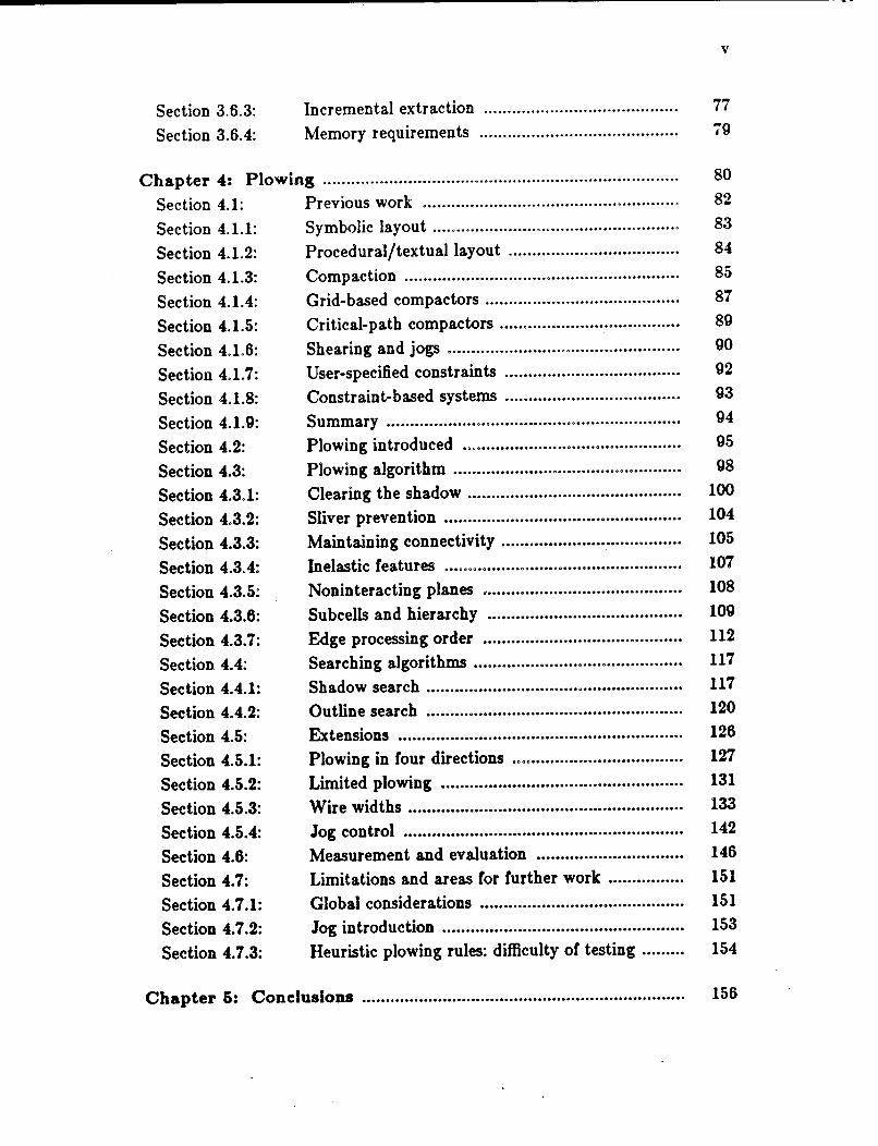
Flsure l.la Seml-cudom aad full-cu.tom methodoloslea. Four
common design methodologies spanning most or the range or choices ror VLSI are
gate-array, standard-ceJJ, macrocell, and ruJJ-customo Gate-arrays (a) consist or
rows or identical cells or transistors. The designer specifies which or a coJJection or
standard metal interconnect patterns to place atop each cell, thereby defining a
given logical function, and how the terminals on each cell are to be connected.
Gate-arrays are the least expensive to fabricate, since the underlying array or
transistor cells can be mass-produced independently or the metal interconnect that
is added later. Standard-cell designs (b) also make use or standard logical functions,
but are not implemented atop an underlying array or identical transistor cells.
Instead, the placement or cells within predefined rows or columns is under the
control or the designer. Because the underlying transistor pattern can vary from
cell to cell, standard-ceO chips cannot be built atop pre-made transistor arrays and
so are more costly than gate-arrays. Figure (c) is typical or the last two
methodologies, macrocell and full-custom. Designs using macrocells orrer still more
nexibility than standard-cell designs: the macrocells are parameterizable, rectilinear
blocks that are customized from a library or templates; these cells are either
connected by abutment or by automatic routing. In full-c:ustom designs, there are
no restrictions on the components; the designer has complete nexibility to create
new circuits and to lay them out in the best possible way.
Activity Gate array Standard cell Full custom
Logic design and simulation 11 15 19
Circuit design 1 1 7
Layout 2 2 20
Total 14 18 46
Ratio 1.0 1.3 3.3
Table 1.11 RelaU~e deals• tlmea for JCa. These figures come from
(RSSSSI and show the relative design times for full-custom versus two semi-custom
methodologies, for comparable 2000-gate circuits. Nearly all or the additional cost
or full-c:ustom comes from the need to design each circuit and each piece or the
layout from scratch.
2
Chips designed using the full-custom approach take longer to
design mainly because more aspects of their layout are under designer

3
control. For example, the designer creates each circuit transistor-by
transistor, rather than from a standard collection of logic gates. Also,
the layout of a given circuit Is not standard, but depends on where
that circuit is used on the chip. Components are often connected by
abutment or local hand-routing, instead of through standard routing
channels by an automatic router. The lack of automatic tools for
full-custom cell design makes these cells time-consuming to enter and
even more time-consuming to change.
In addition to being harder to edit than their semicustom
counterparts, full-custom designs are harder to debug once they have
been laid out. The "debug cycle" consists of alternate phases of
simulation of a layout, followed by changes to the layout to correct
errors discovered during simulation. Because the full-custom layout IS
non-standard, a necessary but time-consuming prelude to simulation IS
circuit extraction, determining the circuit actually implemented by a
custom-drawn layout. Correcting errors once they are found may
require changes to the circuits themselves, instead of simply changes in
how they are connected, and is therefore considerably more expensive
than the re-routing required by simpler methodologies.
This thesis introduces two tools for reducing the cost of the full
custom debug cycle: a fast, incremental, and hierarchical circuit
extractor, and a new operation called plowing for interactively

4
stretching or compacting parts of a layout. The circuit extractor is
considerably faster than previous extractors, less restricting ot design
style, and produces more information about the circuit, including
detailed parasitic resistances and capacitances. The combination of a
fast extraction algorithm and the ability to run incrementally make it
possible to re-extract in minutes a chip that previous extractors took
hours to process. Plowing works directly on the physical mask
representation of a layout, allowing portions of it to be rearranged
while preserving connectivity and layout-rule correctness. It allows
changes to be made more easily to existing layouts as well as speeding
the entry of initial layouts. Both tools have been implemented as
part of the Magic VLSI layout system (OHM85)o
1.1. Circuit extraction
This thesis introduces a fast, incremental, and hierarchical circuit
extractor. It converts the geometry in a layout into an electrical
network composed of transistors and interconnecting material, computing
estimates for parasitic resistance, capacitance to substrate, and coupling
capacitance.
The extractor is built around two new algorithms. The frrst, a
fiat extraction algorithm, operates on mask information only, such as
found in the leaf cells of a hierarchy; it ignores any hierarchical
information that might be present. The second, a new hierarchical

'
5
extraction strategy, makes use of the flat extraction algorithm to
compute connections and adjustments to the circuits of subcells.
The flat extraction algorithm IS based on the idea of
flood£ng-starting at one point and visiting its neighbors
recursively-and the use of a data structure known as corner-stitching
[Ous84a) for speed. The algorithm determines how the transistors in a
layout are connected, computes the capacitance and resistance of the
wires interconnecting these transistors, and finds the coupling
capacitance between pairs of interconnecting wires. It runs 3 to 5
times faster than the fastest previously-reported flat extractor, ACE
from CMU [Gup83), yet produces more information about resistance
and capacitance. It IS over 20 times faster than DEC's IV [TaH83),
one of the fastest industrial extractors (Wil84} that extracts
approximately the same amount of information as Magic.
The new strategy for hierarchical extraction has a number of
advantages over previous approaches. It allows nearly arbitrary
overlap between cells in a layout. Unlike other strategies for
hierarchical extraction in the presence of overlap, it is also able to
preserve the original hierarchical structure. It correctly computes
resistances and capacitances in the presence of hierarchy. By taking
advantage of regular structures such as arrays, and making use of the
flat extraction algorithm described above, it runs very quickly.

6
The most important feature of this hierarchical extraction
algorithm, however, is that it can be used incrementally. Because of
the way it makes adjustments for connectivity, resistance, and
capacitance in the parent of the connected or adjacent cells, changes
to a parent cell do not require its subcells to be re-extracted. Hence,
only those cells that have changed, along with all their ancestors, need
to be re-extracted when the layout changes.
The combination of the two new extraction algorithms make it
possible to extract complete chips in under 20 minutes*. For example,
the entire SOAR chip [UBF84), a 37,000 transistor n~IOS
microprocessor, takes IQ minutes to extract completely. However, it is
almost never necessary to perform a complete re-extraction after
making changes to the layout. In the case of SOAR, the typical
incremental re-extraction time between 5-8 minutes.
1.1. Plowia&
Plowing is a new method for modifying layouts. It works directly
on the mask-level representation or a layout. The plow operation
allows a designer to move one or more pieces of geometry, without
fear or destroying the layout's function: plowing stretches and compacts
other geometry as needed to maintain the circuit's connectivity and
• CPU time on a V AX-11/780, running version 4.2 or Berkeley UNIX

7
the geometries of its transistors while also preservmg layout-rule
correctness.
The plow operation simplifies the job of making topological
changes to a layout. Designers may use plowing to rearrange the
geometry of a subcell, compact a sparse layout, or open up new space
in a dense layout. In a hierarchical environment plowing also allows
cell placement to be modified incrementally without the need for
rerouting.
Previous work aimed at making layouts eas1er to modify has
focused on providing the user with an easy-to-modify representation,
such as a symbolic layout or a procedural or textual description, and
then using an automatic compactor to produce physical mask geometry
(Bal82,Hsu7Q,Kin84,LeM84,Li\V83,MNE82,Mos81, ZDC83J. In most of
these systems (BMS81,da84,LNS82,RBD83, Wes81a, Wil78J, the placement
of circuit components is relative; sizes and spacings are not determined
until compaction. As a result, the designer has fewer constraints to
worry about when placing pieces in a layout, so it is easier to make
individual changes.
Unfortunately, automatic compaction often produces unpredictable
results. This forces designers to iterate several times before achieving
the desired result: make a change to the original layout description,
compact, look at the result, then return to change the original

8
description if the result is not quite right. As a result, while each
change is easier to make, this unpredictability means that many more
changes are required to achieve the desired layout.
The plow operation avoids these problems. It works locally,
moving as little material as possible, which makes it more predictable
than compactors that act globally. · Also, rather than working with
two representations-symbolic and physical-designers who use plowing
always work simply with mask layout. While some of the advantages
of symbolic systems, such as the ease with which they can be
converted to new sets of layout rules, are lost by working with a
single physical representation, I believe that the net gain in editing
efficiency offered by plowing will often more than compensate for this
loss.
The implementation of plowing uses an algorithm that is novel in
several respects. It operates directly on mask geometry, rather than
on a symbolic layout or set of constraints as have previous systems.
In effect, plowing derives constraints from the layout dynamically as it
progresses. Because it uses corner-stitching, 1n which edges are
effectively pre-sorted, it runs in linear time in the number of edges it
affects. When used for compaction, it produces layouts with areas
comparable to those produced by the best one-dimensional compactors,
with running times as good or better.

Flat extraction speed: 25-35 retsfsecond
Flat extraction with substrate capacitance only: 50-65 retsfsecond
Time for incremental re-extraction or 37,000 ret chip: 5-8 minutes
Time to rearrange a 20-transistor cell (several plows): 5 minutes
Time to compact Deutsch's Difficult Example: 1.5 minutes
Table 1.1: Sammar7 of lmpor~aat reaalta. Times and speeds are
reported on a V AX-11/780. Deutsch's Difficult Example refers to the routing
produced by Magic's channel router (Ha084J when run on a routing channel
reported by Deutsch.
1.2. Contributions
g
This thesis presents two tools that shorten the debug cycle for
custom IC layouts. Table 1.2 summarizes several of the benchmarks
that have been used to evaluate these two tools. The results for
circuit extraction are clear-cut; what used to take hours can now be
done in minutes. While it is difficult to quantify the effect that
plowing bas on reducing the overall time required to make layout
changes, it is clear from these benchmarks that major rearrangement
or a cell can be accomplished in a small amount or time. The
combination or these two tools changes the character or the debug
cycle, as shown in Table 1.3. Whereas extraction and layout
modification previously accounted for the maJor fraction or debug time,
now the dominant component is simulation.
In addition to the high-level contribution or speeding the debug
cycle for custom IC layout, this thesis introduces a collection of new
techniques for obtaining geometric and topological information from a
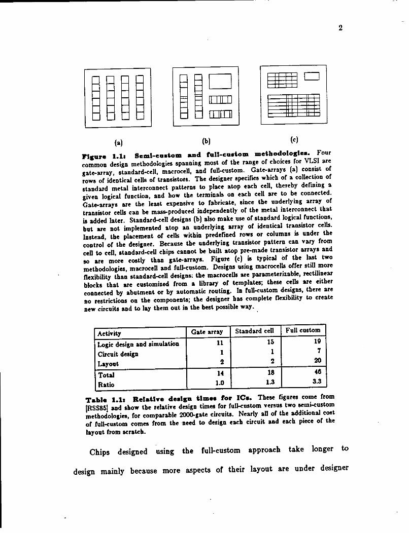
Tlmlns anal7•l•
Previous Magic
Activity time (minutes) percent time (minutes) percent
Layout change 30 26% 5 33%
Extraction 80 70% 6 40%
Crystal !Ous84b] 4 4% 4 27%
Total 114 15
Losle •lmulatloD
Previous Magic
Activity time (minutes) percent time (minutes) percent
Layout change 30 21% 5 12%
Extraction 80 58% 6 14%
Esim !Ter83] 30 21% 30 74%
Total 140 41
Table l.aa Time apeat Ia the debus e7ele. This table compares
estimates or the time spent in various parts or the debug cycle Cor the SOAR chip, a
37,000 transistor 32-bit microprocessor designed at UC Berkeley !UBF84J, with and
without using the tools presented in this thesis. The overall result is that now
simulation is by Car the dominant component or the debug cycle.
10
layout. Examples include finding regions or connected material,
computing w1re widths, finding nearby edges, and tracing transistor
outlines. The techniques make extensive use or corner-stitching, the
data structure used to store layouts m Magic [OHM85). Although
these techniques are presented in the context or plowing and circuit
extraction, I believe they are a generally-useful addition to the
repertoire or computer-aided design tool builders.
1.3. Thesis organisation
The next chapter or this thesis provides an introduction to the
representation of layouts in the Magic system. After describing the

-
I'-
11
meanmg of the tw<rdimensional mask patterns used in IC fabrication,
and the hierarchical layouts used to represent them, it introduces
corner-stitching [Ous84a], the data structure used to store these
patterns m Magic. Corner-stitching is the basis for the logs
representation of a layout used in Magie, and is also used to store
hierarchical designs.
The following two chapters comprise the bulk of this thesis, each
presenting a new tool.
Chapter 3 presents Magie's circuit extractor. After explaining the
role of a circuit extractor and reviewing previous extraction algorithms,
the chapter presents the two new algorithms that Magie's extractor is
built around. Next, it compares both the speed and accuracy of the
new extractor with previous ones. It concludes by suggesting several
ways in which the extractor can be made even faster.
The other tool, plowing, is the topic of Chapter 4, which
describes why custom layouts are so difficult to modify and reviews
previous systems that have attempted to improve custom modifiability.
Next, it presents the plowing operation and the algorithm used to
implement it, along with a variety of extensions that have been made
to improve the usefulness of plowing. Measurements of the overall
effect of plowing on the time spent in the debug cycle have not been
made, but this chapter does present some metrics for comparison with

12
other systems: the speed of plowing, and the area of the layouts it
produces. The chapter concludes with a discussion of problems with
plowing, its limitations, and areas for further work.
Chapter 5 summarizes the ideas and results presented m this
thesis. In particular, it brings together many of the common features
of both the circuit extractor and pl()wing. It discusses the lessons
learned from the implementation of both tools, and it suggests further
applications of the ideas of this thesis.
13
Chapter 2
Layout Representation in Magic
The layout of an integrated circuit IS a ~ollection of twcr
dimensional patterns that describe how to fabricate the circuit. Any
system that manipulates an IC layout must represent these patterns
using data structures suitable to the operations that the system
performs. Magic uses a novel data structure called corner-stitching
[Ous84a) for representing layout.
This chapter begins with some background on how masks are used
to fabricate integrated circuits. Next, it introduces Magic's approach
to representation: the corner-stitching data structure, and the logs style
[OHM85, Wes8lb) of representing abstract rather than physical mask
layers.
The other idea reviewed in this chapter is hierarchical layout,
which allows designers . to express regular structures succinctly and to
organize their designs In a comprehensible fashion. Magic is a
hierarchical layout system; the last part of this chapter explains how
corner-stitching is used to represent hierarchy.

14
2.1. MMka and IC fabrieation
An integrated circuit is defined by a set of masks. These masks
specify regions of the surface of a silicon wafer that are exposed to
various processmg steps during IC manufacture. They correspond to
regions where material IS to be deposited, regiOns where it IS to be
etched away, regions where Ion implantation occurs, etc.
Some circuit structures require only a single mask layer to define
them. Interconnecting wires made of materials such as metal (e.g.,
aluminum) or polysilicon (polycrystalline silicon) are good examples of
such simple structures. The mask layers are often independent of
each other. For example, metal can cross polysilicon without forming
any new circuit structure.
Other structures are more complex, as shown in Figure 2.1. For
example, an nMOS enhancement mode transiStor IS formed m the
ditr enhancement-ret ditr depletion-ret ditr buried-contact
poly
implant buried
(a) (b) (c)
Flaure 1.11 Complex drudure•. Structures iD nMOS such as
enhancement transistors (a), depletion transistors (b), or buried contacts (c) require
more than a single mask layer to define them. Similar structures exist in CMOS,
e.g., p-type and n-type transiston.

15
region where both the polysilicon and diffusion masks are present.
Depletion-mode transistors are even more complex, requiring an implant
mask in addition to polysilicon and diffusion. Physical mask editing
systems such as Caesar [Ous81) define such constructs implicitly by the
overlap of the constituent mask layers. As we shall see shortly,
however, Magic defines them instead via "abstract" layers which are
then used to generate the physical mask layers at fabrication time.
The most general mask shapes are simple polygons. However,
much simpler algorithms for design tools are possible if these polygons
are restricted to have sides parallel to either the z- or the y- axes.
This style of layout lS often referred to as Manhattan. Magic
supports only Manhattan layouts. Although Manhattan designs are
typically 5-10% less dense than designs that contain arbitrary angles,
tools to manipulate Manhattan designs are simpler to build and usually
capable of greater performance than if they had to handle non
Manhattan geometry [Fit82).
2.2. Corner-stltehins
Corner-stitching is the new data structure used by Magic for
representing a collection of non-overlapping rectangles. Each corner
stitched structure is referred to as a tile plane, because Manhattan
regions of arbitrary shape are built up from non-overlapping
rectangular tiles. An unusual property of corner-stitching is that

;--···················································································~ . : [··+······································t·· : ······················~
t-l············~·······t·· !
r-1----~!---t I r-·········································· ·····················•l ... ;
+::ti' t: ::: ' : ul:--_:t : ~
7. .•........................ : ........................................................... 1
Flsure J.Ja Corner-atltchlns. Every point in a corner-stitched plane is
contained in exactly one tile. In this case there are three solid tiles, and the rest of
the plane is covered by space tiles (dotted lines). The space tiles on the sides extend
to infinity. In general, a plane may contain many different types of tiles.
16
empty space is represented explicitly by tiles whose type is "space".
As a consequence, each plane IS completely covered: each point IS
contained in exactly one tile. Figure 2.2 illustrates a corner-stitched
tile plane.
RT
LB
Flsure J.3a Tile and dltche•. Each tile has four 8titche8 that point to its
neighbors. Two are in the top-right corner: RT pointing up and TR pointing
right. The other two are in the lower-left corner: LB pointing down and BL
pointing left.

17
Tiles in a plane are linked to their neighbors by four pointers,
called stitches: two in the upper-right corner of the tile, and two m
the lower-left, as shown in Figure 2.3. The stitches provide a form of
two-dimensional sorting. For example, starting with one tile and
always following the rightward-pointing TR stitch, one visits
horizontally abutting tiles with continuously increasing left-hand
coordinates.
The combination of this two-dimensional sorting and the explicit
representation of empty space make a variety of efficient searching
algorithms possible. Furthermore, updates are very fast m this data
structure, making it well-suited for use m an interactive layout editor
such as Magic. Many of the basic algorithms for searching and
updating corner-stitched planes are described in Ousterhout's paper that
introduces the data structure (Ous84a].
2.3. Loss
Corner-stitching alone is unable to represent overlapping rectangles.
In a real layout, however, overlaps are common, both between
independent mask layers, such as polysilicon and metal, and between
mask layers that together create a circuit structure, such as polysilicon
and diffusion. Some additional structure is required on top of corner
stitching to represent these overlaps.

(a)
(b)
(c:)
Flpre 2.41 0Yerlap• Ia Maslc. There are two choices for representing
overlapping mask layers (a) in Magic. Where the overlap or the two layers does not
form a new circuit component, as is the case with metal and polysilicon, they are
stored in separate tile planes sharing the same coordinate system (b), Where the
overlap does form a new component, as when polysilicon and diffusion overlap to
make a transistor, both layers are stored in the same tile plane and the overlap area
is marked with a special type of tile (c).
18
Magic's approach to representing them has two parts, shown in
Figure 2.4. Where the potentially overlapping materials do not form
new structures, they are stored in different tile planes. Where new
structures are formed, the overlapping materials are stored in the same
tile plane and the overlap lS marked as having a special tile type.
This idea of special tile types is taken one step further by what
is called the logs style of layout representation after Neil Weste
[Wes81b). In the logs style, regions containing a single mask layer,
such as polysilicon, metal, or diffusion, are easy to represent; they are
I ....
Magic layer
poly silicon
diffusion
metal
enhancement ret
depletion ret
buried contact
poly-metal contact
diU-metal contact
Physical mask layers
poly silicon
diffusion
metal
contact
implant
buried
Magic plane(s) Constituent layers
active poly silicon
active diffusion
metal metal
active polysilicon, diffusion
active polysilicon, diffusion, implant
active polysilicon, diffusion, buried
active, metal polysilicon, metal, contact
active, metal diffusion, metal, contact
Table 1.11 NMOS la7era. The first table shows the physical mask layers,
and the second shows the Magic layers and the planes on which they are stored.
The nMOS process has buried contacts and a single level or metal. Since polysilicon
and diffusion form transistors when they overlap, they are placed in the same plane.
Metal interacts with polysilicon and diffusion only at contacts, so it is placed in a
separate plane. Contacts between metal and diffusion or polysilicon are duplicated
in both planes.
stored as rectangles or the mask layer they contain. Regions where
mask layers overlap to form electrically significant constructs, such as
enhancement-ret, are represented as distinct objects instead or implicitly
by the overlap of their constituent mask layers. Furthermore, non-
conducting layers such as implant, well, or buried-contact masks are
not stored at all; instead, structures that would be overlapped by
these masks are stored as tiles or different types.
Storing a layout as logs results in a slightly different set of layers
than physical mask layers. However, the number or logs layers is
(a) (b)
(c) (d)
l'lsure 1.&1 Los• la7out. This figure compares a physical NMOS layout (a) with its representation in Magic (b). The Magic version bas two planes; (c) shows the active plane, containing polysilicon, diffusion, and their overlaps; (d) shows the metal plane. Contacts are duplicated in each plane.
20
usually close to number of physical layers. Table 2.1 compares the
Magic layers with the physical mask layers for a simple nMOS
fabrication process, and Figure 2.5 compares Magic's version of an
example cell with the physical mask version. See the reports
(Sco84, SHM85) for complete details on how logs layers are chosen for
a given set or physical mask layers.

21
2.4. Hierarchy
Fabricating an IC reqmres knowledge only of the mask patterns
that define its circuit. However, it is often convenient to impose
additional structure on these mask patterns, to make them more
manageable. Organizing the layout into a hierarchical tree of cells 1s
a useful. way of imposing structure; this approach has been taken by a
number of layout systems [KeN82a,KeN82b,Ous81,RBD83, Wes81a).
Cells in a hierarchical layout may contain mask information, or
they may contain other cells, known as subcells. In some systems,
lr ............... l ................. .................
: jjjjji··· . : I ;:;: I I :::: I
r---------
I I I
I I I L~-=:::::__
ROOT CELL
(a)
c B
(b)
Flsure 1.8a Blerarehleal la7out. The root cell in (a) contains both mask
inrormation and two subcells, A and B. Subcell A in turn contains two subcells, B
and C, each or which contains only mask inrormation. A schematic representation
or the hierarchy is shown in (b). Both instances orB rerer to the same cell.
22
such as Magic, cells may contain both kinds of information. When a
cell contains a subcell, it is interpreted as containing all the mask
information in that subcell, plus all the mask information in all that
subcell's subcells, etc., down to cells that contain only mask
information. See Figure 2.6 for an example.
Hierarchical design has a number or advantages. If a chip is
broken into cells along functional boundaries, it is usually much eas1er
for designers to understand. Multiple designers can each work on a
piece of a hierarchical layout without interfering with each other. In
addition, hierarchical designs are modular; cells may be placed or
moved as entire units, and a single cell may be used in many
different places in the design. Regular structures such as arrays are
easy to represent in a hierarchical system. Hierarchy benefits CAD
tools by reducing the amount or work they must do to process
repetitive structures; this fact is central to the speed of Magic's circuit
extractor.
Although hierarchical structure has advantages, sometimes it lS a
hindrance. Sometimes tools need all material in a particular area,
without caring which cell the material came from. This occurs, for
example, when generating masks to fabricate the chip, and also during
operations such as circuit extraction or routing. A common way or
finding all material in an area is to flatten a hierarchical layout by

I---- -r I A I
I
l---- _I
(a)
,--,-- r- -, I I I
dJ:Jl
I I
'-- .J-- l..- _, B
(b)
B
(c)
Flsure 1.'11 FlaUealas a hierarchical de•lsa. The subcell A in (a) is
used twice in cell B in (b), once in its normal orientation and once mirrored about
the Y axis. The result or nattening is shown in (c), where the mask inrormation in
the two instances or A has been merged and replaces the two cell instances in the
parent B.
23
converting it into a single set oC mask layers that represents the entire
hierarchy, as illustrated in Figure 2.7. Since flattening requires extra
computation in addition to increasing the total amount o( information,
it is generally best to develop tools that can work directly (rom a
hierarchical layout, or which can be selective and only flatten a small
fraction or the entire layout.
Z.&. Corner-stitching and hierarchy
Subcells in Magic may overlap each other, just as mask
information may overlap other mask information. Similar alternatives
to those Cor allowing mask overlap are possible Cor allowing cell
overlap in a corner-stitched data structure. Since it lS impractical to
store each subcell on a different plane (the number or subcells in a
given cell may be large), Magic stores all subcells in the same plane,

or--------,·························
B B
B A,B B ~-!-----+---"·························
A A
A A,C C
c .................... L------l,__---L-----1
c .............................. ......_ _____ ___._
(a) (b)
Figure 1.81 Overlapping •ubcell•. The collection or overlapping subcells
A, B, and C in (a) is represented by the tiles in (b). Each tile points to the cells that
overlap it. Furthermore, the plane is broken up into tiles in such a way that a cell
overlaps a tile either completely or not at all.
24
and represents overlap areas by tiles of different types, as shown m
Figure 2.8. Each tile points to a list of the cells that overlap it.
When no cells overlap a tile, that tile points to an empty list. The
plane is divided into tiles in such a way that each tile corresponds to
a particular combination of overlaps.
Magic's approach pays a price in complexity when massive overlap
occurs at the same level of the hierarchy, requiring in the worst case
2N tiles for N overlapping cells. Fortunately, this worst case almost
never occurs in practice; it is rare for more than 4 cells to overlap at
a given point in a design. Furthermore, designers are encouraged to
use a style in which cells nearly abut, except for a small area of
overlap near their edges.

....... 25
2.1. Summary
The use of corner-stitching to represent a layout as logs is
particularly well-suited to circuit extraction and plowing. The
following list summarizes the major reasons why:
• Connectivity is represented explicitly via the corner-stitches. Nearby material is also easy to find by taking advantage or the stitches. Algorithms for tracing connectivity and finding neighbors will be presented in the next two chapters.
• Electrical constructs, such as transistors and contacts, are represented explicitly. Plowing can move them intact as objects, and neither the extractor nor plowing have to recompute them by searching for overlaps.
• Layers with design-rules between them are stored on the same plane. Layers that don't interact are stored on different planes. Contacts are stored on each of the planes that they connect.
• Subcells are stored using a different "tile type for each different overlap area, so finding overlapping or abutting cells is easy.

26
Chapter S
Circuit extraction
The first step m verifying a custom VLSI design-by simulation,
timing analysis, or electrical rule checks-is circuit extraction. This
operation converts a mask-level layout into an electrical network or
transistors, interconnecting wires, resistances, and capacitances that IS
equivalent to the circuit implemented by the layout. Verification tools
are then applied to this extracted circuit. During the debug cycle,
circuit extraction is performed many times; it must be repeated each
time the layout is changed to nx a bug discovered during verification.
Unfortunately, with ever-increasing circuit sizes circuit extraction
has become extremely time-consuming. At UC Berkeley, even using a
relatively fast circuit extractor [Fit82), extracting a 40,000 transistor
chip takes several hours. For industrial extractors that provide more
detail in the extracted circuit, times are typically an order or
magnitude greater [TaH83). Much of the time spent in these circuit
extractors is wasted; even after a small change to the layout, the
entire process of extraction must be repeated. The result is a debug
cycle that takes hours or days for each change.
This chapter presents a new circuit extractor that dramatically
reduces re-extraction times, to on the order of ten minutes or less. It

uses three techniques to achieve this:
• A fast new "flat" extraction algorithm, based on corner-stitching, for
extracting the circuit from a layout that contains no hierarchy.
• A hierarchical extractor, built on top of the flat extraction algorithm,
that exploits regularity for speed.
• An incremental extraction strategy in which only a small fraction of
the cells in a layout must be re-extracted after small changes.
27
The first section of this chapter discusses circuit models: what
information 15 present in the circuit description produced by an
extractor. It compares several different models, and then describes the
choice taken in Magic.
The next three secti<?ns present Magic's circuit extractor. Section
3.2 introduces Magic's fiat extractor, which uses a novel flooding
algorithm based on corner-stitching. The flat extractor is used for
computing both connectivity and internodal coupling capacitances.
Section 3.3 focuses on extracting hierarchical layouts. It explains
the advantages or producing hierarchical circuit descriptions that
parallel the structure of the original layouts. Then it describes
Magic's hierarchical extraction strategy, which is based on extracting
each subcell independently, and then making connections and
adjustments to parasitic resistance and capacitance between subcells in
the parent containing them. The algorithm to implement this strategy
processes only those regions where material from more than one cell is

28
present, and takes advantage of arrays to run very quickly. Section
3.4 concludes the presentation of Magic's extractor by describing how
it performs incremental extraction. When any cell in the hierarchy
changes, only that cell and its ancestors must be re-extracted, avoiding
most of the work of extraction after small changes to a layout.
Section 3.5 presents performance measurements. They show that
Magic's extractor is about 5 times faster than ACE [Gup83], the
fastest previously reported circuit extractor. When extracting
incrementally, it is even faster; the same 40,000 transistor chip that
used to take hours to extract can now be re-extracted incrementally in
5-10 minutes. Magic's approach is not without limitations; these are
discussed in Section 3.6, along with areas for further work.
1.1. Circuit models
An extracted circuit is the input to a wide variety of verification
tools. For example, the extracted connectivity of a layout can be
compared with that of an independently-drawn schematic to ensure
that it is the same [CHY80, KKY70, Spi83, TMC82). In ratioed logic
such as nMOS, the sizes of pullup and pulldown transistors can be
compared to ensure that they meet certain rules (SHM85). The circuit
implemented by the layout can be simulated, and the results of the
simulation can be compared to a specification or to the results of a

-
2Q
parallel, functional simulation [BaT80,Bry81). A timing verifier can
compute the delays through a circuit to determine whether it meets its
timing requirements (Jou84, Ous83). Finally, a detailed analysis can be
performed of the waveforms propagating through the circuit
(LeS82,NaP73).
The amount of detail required from an extractor depends on the
kind of verification to be performed. Figure 3.1 illustrates a simple
layout and several choices for extractor output. To perform a netlist
comparison, for example, it is sufficient to extract a list of all
Vdd
(a) (b)
Vdd Vdd
Out (c) (d) Out
~ In ~ :r:: ":" ":" Phil
":"
Figure 3.11 Detail Ia aa extracted elrcult. A simple layout is shown in
(a). Different extractors extract different amounts or detail, as shown in (b)- (d).
The output in (b) contains only the locations or transistors and connectivity, (c)
contains transistors sizes and lumped per-node capacitances !Fit82J, and (d) contains
a detailed RC-network model or the circuit !McC84J.
30
transistors in the design, and how their gates, sources, and drains are
connected. Examples of extractors providing only this information are
[Wag84) and DPL/Daedalus [BMS81]. Adding the length and width of
each transistor's channel to this list makes it possible to perform
switch-level simulations and transistor size ratio checks. In MOS
circuits, however, the resistance and capacitance of interconnecting
wires play a significant role in determining whether or not a circuit
will work, and how fast it will run. If the output of an extractor is
to be useful for timing analysis or detailed circuit simulation, it must
include the "parasitic" resistances and capacitances (shown in Figure
3.2) as well.
One approach, taken by EXCL [McC84) and SPECS [BHE83), is
to describe interconnecting wires as a detailed RC network, as shown
in Figure 3.1d. This approach has the advantage of accuracy, but the
detailed descriptions it produces are unnecessary for many digital
applications (Ous84b), and are excessively bulky for large _layouts.
A simpler approach is to lump each region of interconnecting
material that contains no transistors into a single electrical node.
Each node includes a lumped parasitic resistance and capacitance to
ground, as shown in Figure 3.3. Nodes are a simplification over
detailed resistors because the path between any two transistor terminals
connected to a node is assumed to have the same resistance. The

(a)
(b)
(c)
3 squares
3 squares
. . . . .
metal-1
C3
_ C2
_ _ silicon dioxide
f:~f~~M~~~f~~U~i~i~~~~~~!~Ji- silicon ( GND)
___ _top _!i!_w _________ e~d_ v!e! ___ _
..-----metal-1
metal-2 metal-2
top VIeW
Flsure 3.1: Para.ltle real.tauee aud capacitance. Interconnecting
wires in VLSI layouts have resistance and capacitance. Resistance depends on the
conductivity or the interconnecting material. Because the height or all wires of a
given type is constant, the resistance or a wire remains the same if its width and
length increase by the same factor; resistance is therefore proportional to the
number of "squares" in a wire. In (a), both wires have the same resistance between
points 1 and I. Capacitance occurs across the dielectric oxide, either to the ground
plane or to adjacent or overlapping wires (b, c).
31
node approach has been used successfully by a number of extractors,
such as MEXTRA (Fit82}, MART [NeS83), and others
[Bak80,Fit83,GiN77,MCT80,RBD83, Wei84, Wes81a, Wil81,Yip84), and
simulation tools, such as Crystal [Ous83), and Esim [Ter83).
Greater accuracy in simulation is possible by adding coupling
capacitances between parallel or overlapping wires that belong to
different nodes, as IS done 10 IV [TaH83). Coupling capacitance
N 1
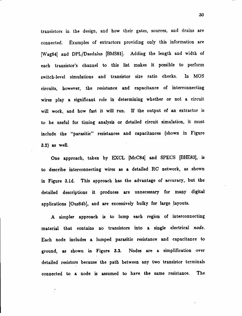
l'lpre 1.11 Lumped aodal B aDd C. A node with resistance R and
capacitance C is interpreted aa the network shown above (Oua84bJ. Each or the
points 1, e, ... , N above is a connection to the node by some terminal or a device.
The approximation is that the resistance between any two terminals connected to
the node is always R, regardless or how close or rar apart they really are.
32
becomes particularly important as feature sizes shrink; in one industrial
example (Jou85) only 4.8% of one node's capacitance was to ground;
the remainder was coupling capacitance to other signal lines.
The extractor described in this chapter takes the node-extraction
approach, adding coupling capacitance between nodes where it 18
significant. The resulting circuit description contains three kinds or
components: nodes, transistors, and capacitors. Figure 3.4 shows the
result or extracting a simple Magic layout.
3.2. Flat extraetloa
At the heart of any circuit extractor is a "fiat" extractor that
works directly on mask geometry, ignoring any subcells that might be
present. A fiat extractor is responsible Cor finding the connected
geometrical regions that make up the nodes and transistors in the

aode GND 12 21
•od• 8150 50 aode 1.4.8of 10 I
(e) aode A 150 50 •od• Out 111 25 aode Vdd 22 210
cap8A2
Out Node: Vdd
(b)
Node: 1.4.8of
Node:GND
re' elet 12 11 GND 8 4 1.4.8of I GND I
re' elet 12 11 GND A 4 Out I II. 4.8of I
'•' dCet 12 11 GND Out 12 Vdd 2 Out 2
Flpre 1.41 Mapc•a circuit for a la7out. The layout in (a) is a simple
nMOS NAND gate. Magic extracts paraai_tic resistance and capacitance along with
transistors and connectivity. In addition, it extracts coupling capacitances where
significant. The result is shown in (b). The actual output or the extractor is shown
in (c). Note the three types or components: nodes (aode), capacitors (cap), and
transistors (let). Each node has a name, e.g., "GND", "B", "3.4.6#", which is
used in transistor or capacitor terminals to specify connections to the node.
33
layout. In addition, it detects nodes that are close to each other so
that coupling capacitance between them may be computed.
3.2.1. Pre..-loua work
Perhaps the simplest fiat extraction algorithm uses flooding, an
idea developed for filling polygonal regions on raster graphics displays
(Lie78,Pav8l,Smi7Q). The fiooding algorithm uses an array of pixels,
one for each unit square in the layout. Each pixel contains the types

34
of material present in it. To find all material connected to a gtven
pixel, its neighboring pixels are visited recursively. The recursion stops
when a pixel is seen that has already been visited, or when a
neighboring pixel contains no material that connects to that in the
current pixel. Figure 3.5 gives an example of flooding.
Although flooding is simple, it requires excessive amounts of mam
memory to represent all the pixels in a large design. For a chip
occupying a die 5000 microns on a side, designed on a 1 micron grid,
with one byte per pixel, the memory required would be on the order
or 25 megabytes! Because or its large memory requirements, flooding
l'lpre 1.5• l'loodlas alsorllhm. Each pixel stores the type of material
present beneath it. Starting from a single pixel inside a node (a), it is marked and
its immediate neighbors are visited and marked if the material they contain is
connected to the original pixel (b). This process proceeds recursively for each
marked pixel (c:) until all pixels in the node have been marked (d).

35
has not been used much in practice.
Another approach that is nearly as simple as flooding, but with
significantly smaller memory requirements, was described in [Bak80]. It
also uses a pixel map, but since it processes the layout in order from
top to bottom, it only keeps a single row ("scan-line") of pixels in
memory at once. Each pixel in the row IS marked with the material
it overlaps and the electrical node to which this material belongs.
After first sorting all geometry m the design in order of
decreasing greatest-Y coordinate, the algorithm scans from the top of
the design to the bottom as shown in Figure 3.6. Pixels in the
current scan-line are filled in from the sorted g~ometry list, using a
scan-conversion algorithm [Arn85). When processing each pixel, only
the pixels above and immediately to its left need be considered to
1
Flpre l.lh Bitmap extradloD alsorlthm. The bitmtlp extraction
algorithm moves a scan-line across the layout from top to bottom. When
processing a given pixel, the scan line contains pixels in the same row and to the
left, and in the previous row to the right.

36
determine the connectivity, node perimeter, and node area.
This bitmap scan-line algorithm introduces a complexity not
present in the flooding approach. Figure 3.7 shows that it is possible
for two pieces of geometry to start out as two unconnected nodes,
and later have to be merged because they connect on a lower scan-
line. Terminals of transistors connected to these two pieces of
geometry would be output incorrectly as having different node names.
Hence, the scan-line pass must be followed by a second pass to
rename all nodes, resulting in a single name instead of several different
ones for the same node.
(a)
(b)
Dl~
I I l
I I I
l ol merge o2
/D2 I I
J'lsare a.'la Node mer&las Ia the •eaa-llae alsorlthm. Two pieces or geometry that ioitially appear to belong to different nodes (a) may in ract belong to the same node. This ract will eventually be detected when the scan-line progresses rar enough down the layout (b), at which time the two nodes are merged.

significant pixels ....
Flsure a.aa Wh7 bitmap Ia wadeful. Most or the bits in the interior or a
shape contain no information. Changes in connectivity occur only those pixels on
the boundary, which account for less than 5% or aU the pixels in a typical design,
such as the SOAR chip IUBF84J.
37
Both bitmap algorithms have a common problem: they waste most
of their time processing the pixels in the interior of a shape, as shown
m Figure 3.8. The only real information is contained in the boundary
of a shape, so a better approach is to eliminate the bitmap and
process only edges. Doing so typically reduces the amount of
information processed by over an order of magnitude, according to
measurements made by the author of several designs.
The edge-based scan-line extraction algorithm avoids the cost of
processing interior pixels. It maintains a list of vertical edges
intersecting the current scan-line, sorted in order of increasing z-
coordinate. As it processes the scan-line from left to right, the
amount of work done is proportional to the number of edges
intersecting the scan-line, not the number of pixels it contains. Most
extractors use this edge-based algorithm; some well-known examples are

38
MEXTRA [Fit82], IV [TaH83], and ACE [Gup83].
The three algorithms mentioned so far all work directly from
physical layout. Several systems exist that extract a circuit from
different layout representations. EXSIM [Yip84] builds up the
description of the circuit as a layout is being synthesized. VIVID
[RBD83) and i [JoB80), both symbolic layout systems, extract the
circuit topology directly from . the symbolic representation or the layout.
Although this results in fast extraction-one can argue that the
symbolic representation lS "already extracted"-it has difficulty in
estimating parasitic resistance and capacitances, since the final spacing
of components in a layout is not known until physical masks are
generated by a compactor.
3.2.2. Finding nodes and transistors
Magic's fiat extractor is based on flooding, but uses the tiles in a
corner-stitched plane instead of a bitmap of pixels. By processing tiles
instead of pixels, it has the same performance advantages over pixel
based flooding that the edge-based scan-line algorithm has over the
bitmap algorithm, and also requires much less memory. The explicit
representation of connectivity by the corner-stitches, coupled with the
simplicity of the flooding approach, makes fiat extraction extremely
fast.
·····------------------------------------·----------------------------------··------·-----------------·-···-----
5
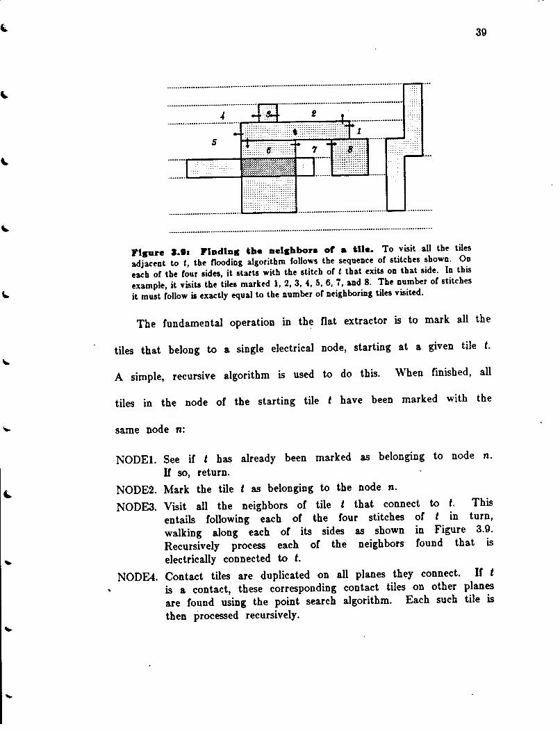
l'lsure a.la l'ladlas the aelshbora of a tlle. To visit all the tiles
adjacent to t, the fiooding algorithm follows the sequence or stitches shown. On
each or the four sides, it starts with the stitch or t that exits on that side. In this
example, it visits the tiles marked 1, 2, 3, 4, 5, 6, 7, and 8. The number or stitches
it must follow is exactly equal to the number or neighboring tiles visited.
39
The fundamental operation in the flat extractor is to mark all the
tiles that belong to a single electrical node, starting at a given tile t.
A simple, recursive algorithm is used to do this. When finished, all
tiles in the node of the starting tile t have been marked with the
same node n:
NODE!. See if t has already been marked as belonging to node n.
If so, return.
NODE2. Mark the tile t as belonging to the node n.
NODE3. Visit all the neighbors of tile t that connect to t. This
entails following each or the four stitches or t in turn,
walking along each of its sides as shown in Figure 3.9.
Recursively process each of the neighbors found that lS
electrically connected to t.
NODE4. Contact tiles are duplicated on all planes they connect. If t
is a contact, these corresponding contact tiles on other planes
are found using the point search algorithm. Each such tile is
then processed recursively.

VJSitTile{t) Tile~;
{
}
Plaae "plane; TUe *t2;
II (Visited( t)) rdara;
M&rkVJ.Sited(t);
;•Tor r for (t2 - RT(t); RIGHT(t2) > LEFT(t); t2 - BL(t2))
II (Connects(t, t2)) VJ.sit.Tile(t2);
;•uft r for (t2 - BL(t); BOTTOM(t2) < TOP(t); t2 - RT(t2))
II (Connects(t, t2)) VJSitTile(t2);
;• Bottom r for (t2 - LB(t); LEFT(t2) < RIGHT(t); t2 - TR(t2))
II (Connects(t, t2)) VJ.sit.Tile(t2);
. ;• Right r for (t2 - TR(t); TOP(t2) > BOTTOM(t); t2 - LB(t2))
II (Connects(t, t2)) VJ.sitTile(t2);
j• Contact• r II (lsContact(t)) {
}
for ( ... each plane t connects to ••• )
{
}
t2 - FindTileContaininr;Point(plane, &t->tile_lowerLeft); VJSitTile(t2);
40
VisitTile
Flsure 3.10a AlsorUhm NODE. This algorithm accepts as input a starting tile in a
node, and recursively traces out all tiles that are connected to the starting tile.
See Figure 3.10 for a detailed description of the NODE algorithm.
The above node-finding algorithm considers two adjacent tiles to
be electrically connected if they appear as a pau in a connectivity
table. This table comes from a technology file, making the algorithm

41
technology independent. By changing this table, the same algorithm
can trace out regions other than nodes. For example, it is used to
find all the tiles belonging to each transisto~ by using a connectivity
table where each type of transistor "connects" only to other tiles of
the same transistor type.
The flooding algorithm does most of the work of extraction. The
only additional component required for extracting all the nodes m a
cell is a procedure to find the starting tile for each node. To find
such a tile, Magic uses the area enumeration algorithm described in
[Ous84a] to visit all tiles in the cell being extracted. If a tile has
already been marked with . a node, it is skipped; otherwise, a new
node is allocated and the node-finding algorithm is applied to that tile.
Each node is given a name. If the designer has attached any
labels to geometry belonging to a node, aU of those labels are
considered to be names for the node. If no labels are present,
however, the extractor generates a unique node name automatically.
These unique node names are generated independently of the order in
which nodes are visited, so the hierarchical extractor can generate
them when it needs to make connections to subcells. For more
details, see the end of the section on hierarchical extraction.

42
dirr-metal-contact
Flsure 3.1la Perimeter capacitance. The perimeter capacitance for a segment or a
tile boundary depends on both the types inside and outside the boundary. In this diagram,
only the boundaries shown in boldface have perimeter capacitance to substrate. For
example, a boundary between diffusion and empty space has a certain amount or perimeter
capacitance. A boundary between diffusion and diffusion-metal-contact has none, because
diffusion-metal-contact contains diffusion when fabricated and hence there is no sidewall
boundary. The amount or perimeter capacitance associated with each type or boundary is
specified in the technoloc rile.
a.2.a. Resistance and substrate capacitance
Magic9S extractor computes a parasitic capacitance to ground and
a lumped resistance Cor each node. Each type or material has a
capacitance to ground per unit area. Each material also has a
perimeter capacitance per unit length that may depend on the types
or its neighboring material as shown in Figure 3.11.
Lumped resistances are computed usmg a very simple
approximation. The extractor computes the total perimeter P and
total area A oC each type or material comprising a node. It then
assumes that this material is a simple rectangular regiOn with the
same perimeter and area, and solves Cor the length L and width W of
the rectangle as follows:

43
P = 2W+2L
A= lt'L
This yields the following quadratic equation:
2x2-Px +2A = 0
The larger value of x is taken as L, and the smaller as W. See
Figure 3.12. The total resistance of the node is taken to be the sum
of the resistance of each of the above regions. Although this
approximation for resistance 1S easily computed, it has its inaccuracies;
Section 3.6.1 discusses these in detail.
The node-finding algorithm is easily extended to compute the
perimeter and area required for calculating capacitance and resistance
as above. The area of the node is just the sum of the areas of each
of its individual tiles, which can be visited using the flooding
algorithm. Each segment of perimeter appears uniquely along the
boundary between some tile inside the node and some tile outside of
(a) l._r= (b) £.;.;.·.·.··:·;·:····-·.·.·.·.·.·.;.·.·.·······-·.·.·.·.;.;.;.;.·.·.·.·.;.·.;-·-·.·.·.;.·.;.·.·.·.·.·.·.;.-.•.·.·.·.·.·.···········································-·.;.·J
Flaure 3.11& Appro:dmatlD& real.taDee. Magic approximates the resistance or the
node in (a) by assuming that it is a simple rectangular region (b) with the same perimeter
and area, and computing the length and width or this region.
44
it. The total perimeter of a node IS computed by modifying step
NODE3 of the previous algorithm:
NODE3. Examine all the tiles s adjacent to tile t as shown in Figure
3.Q. If tile s connects to t, recursively visit s. Otherwise1
determine the length of the segment of boundary common to
s and t and add this to the total perimeter.
For computing perimeter capacitance, instead of computing a simple
sum of the lengths of the perimeter segments, the algorithm computes
a weighted sum of these lengths using different weights for different
types along the perimeter.
3.2.4. Transistors
Magic's extractor recogmzes MOSFET transistors only. A
transistor is assumed to have a gate that covers the channel, and one
or more sources or drains connected to the channel. The terminals of
a transistor are the gate and all the sources/ drains. In addition to
listing the nodes to which a transistor's terminals connect, a
transistor's description includes the perimeter and area of its channel,
and the length of the total channel perimeter occupied by each
terminal.
A single transistor may contain several tiles of the same type.
Figure 3.13 shows an irregularly shaped transistor made up of two
tiles. All the tiles in a transistor are found by usmg exactly the
same algorithm as used to find nodes. Area enumeration is used to

space
······················· • • • • • • • • • • • • • • • • • • • • 0 • •
······················· ······················· ······················· ............. -...... · .. . ............. · ......... . ·····················
45
.............................................
Flsure 3.131 Extraetlas traaal.tora. This transistor, with a non-rectangular
channel, requires two efet tiles to represent it. The same algorithm used to find nodes can
find all connected regions of transistor tiles, so such irregular channels are easily identified.
find the first tile in each transistor, and then the node finding
algorithm IS invoked to find the remaining tiles, usmg a special
"connectivity" table. The perimeter and area or the transistor are
computed in exactly the same way as the perimeter and area or a
node.
Before transistors are extracted, the node-finding algorithm has
marked each tile with the node to which it belongs. Finding the
nodes connected to a transistor's terminals involves simply reading the
nodes from the tiles adjacent to the transistor. This is done by
walking around the perimeter of each tile in the transistor, using an
technique identical to that used in the NODE algorithm for visiting all
the neighbors or each tile.
The type or material adjacent to a transistor will determine the
terminal it connects to. In our p-well CMOS process, for example,

46
polysiliccn adjacent to a transistor connects to its gate, while p-
diffusion forms a source or drain. These types are technology-
dependent, so they are described as part of the Magic technology file.
3.2.5. Couplins capacitance
Coupling capacitance arises when wues on different mask layers
overlap, or when parallel wires run side-by-side. Magic's extractor
computes capacitance due to both causes.
Since tiles can only overlap if they are on different corner-stitched
planes, internodal coupling capacitance due to overlap can only occur
between tiles on different planes. The algorithm for computing overlap
coupling capacitance is therefore very simple. For each tile t in a
plane,
OVERLAP!. Search other planes for tiles that overlap f.
OVERLAP2. Compare the nodes of each tile found with the t's node.
H they are different, record a coupling capacitance
between the two nodes, based on the two tile types and
proportional to the overlap area.
See Figure 3.14 for details of the OVERLAP algorithm.
To avoid detecting an overlap twice, only lower-numbered planes
than that containing the original tile are searched. In our CMOS
process with two levels of metal, Cor example, there are three tile
planes: active (holding polysilicon, diffusion, and transistors), metal1,
and metalf. For each tile in metal1, only active is searched for
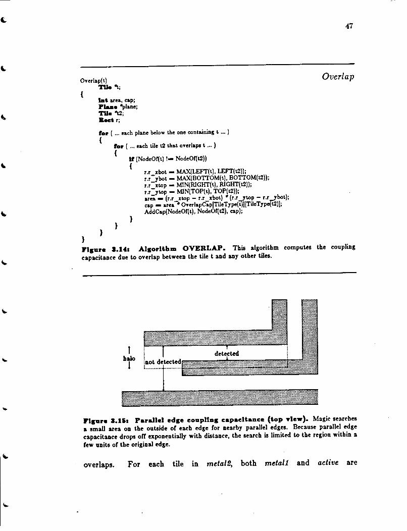
Overlap(t) Tile~;
{
}
lat area, cap; Plaae ~lane; Tile *t2; Jleet r;
for ( ... each plane below the one containinr; t ... ) {
}
for ( ... each tile t2 that overlaps t •.. )
{
}
If (NodeOI'{t) !- NodeOI'(t2)) {
}
u xbot - MAX(LEFT(t), LEFT(t2)); r.r-.rbot- MAX(BOTTOM(t), BOTTOM(t2)); r.r-xtop- MIN(RJGHT(t), RJGHT(t2)); r.rJtop- MIN(TOP(t), TOP(t2)); area- (r.r_xtop- r.r_xbot) • (r.r...J:toP- r.r .rbot); cap - area • OverlapCap!TileType(tJIITileT.rpeft2)); AddCap(NodeOr(t), NodeOr(t2), cap);
47
Overlap
l'lsure J.14a Alsorlthm OVERLAP. This algorithm computes the coupling
capacitance due to overlap between the tile t and any other tiles.
l halo l
::~ l'lpre J.l&a Parallel edse eoupllas eapaeltaaee (top ·dew). Magic: searches
a small area on the outside or each edge ror nearby parallel edges. Because parallel edge
capacitance drops orr exponentially with distance, the search is limited to the region within a
rew units or the original edge.
overlaps. For each tile in metal!!, both metal1 and active are

48
searched. Any material present m meta/1 will mask capacitance
between meta/2 and active over the area it occupies.
Coupling capacitance between parallel edges is computed by first
finding all edges, and then searching the area outside each edge for
nearby parallel edges. Because this kind of capacitance falls off
exponentially with the distance between the edges, the search is limited
to a few units outside the edge. See Figure 3.15.
3.3. Hierarchical extraction
The previous section was concerned with extracting a circuit from
a cell containing mask information alone. In addition to mask
information, cells in Magic may contain subcells. Extracting the
circuits of such hierarchical cells requires additional work beyond what
a fiat extractor is capable of doing.
The simplest method of dealing with hierarchy is to eliminate it.
Extractors such as MEXTRA (Fit82) do so by fiattening a hierarchical
cell into a temporary cell, and then using a fiat extractor to extract
the fiattened cell. Although this strategy is easy to implement, it
does not take advantage or any or the structure present in the
original, hierarchical layout.
A different approach is to extract the circuit hierarchically. There
are really two ways in which an extractor can be hierarchical: it can

49
accept a hierarchical layout as input, and m addition it can produce a
hierarchical circuit description as output.
By exploiting hierarchy on input, an extractor can run faster than
its flattening counterpart. Typical VLSI layouts are highly regular,
with some cells occurring many times, e.g., memory cells or bits in an
ALU. A hierarchical extractor only needs to extract such cells once;
all instances after the first are "free" except for the cost of extracting
connections to them. In comparison, a flattening extractor must do
the same amount of work for each instance of a cell.
By producing a hierarchical output, an extractor allows simulation
and analysis tools to take advantage of a layout's regularity. A
hierarchical circuit representation is more compact, so these tools can
use less memory to store the circuit (Jou84). Also, hierarchy provides
clean boundaries at which pieces of a circuit can be replaced by
simpler macromodels to speed simulation. Finally, smce the
hierarchical circuit structure is identical to that of the layout, users of
analysis tools can use the same node names in each.
When a cell in a hierarchical design contains subcells, its circuit
includes the circuits of its subcells. However, it is not possible simply
to concatenate the subcircuits, since overlaps or abutments can change
their structure radically. As an obvious example, the extractor must
merge nodes in two different subcells that overlap or abut. The

50
- - - - -
~~ I I I I I
~I I
' I
. : I
ii 1ll!lli; ::
I
(a) . I I .
I I I
I I I I
dit I I I I
•- - J I - -· ·- - .1. - -• - - - - -d;tl I I I I I
~I I
1Jj I
. I I .. I
(b) : I lllll~; I
. I I . I I I
po I I I 1- - J I - -· 1- - .. - _,
l'lsure a.tea Tran•l.ton and abutment. Transistors may merge as a result or
subcell abutment. In (a), the result is a longer transistor, while in (b) the result is a wider
one.
transistor structure can change as well: new transistors may be formed,
or existing ones merged or deleted, as shown in Figures 3.16 and 3.17.
Values of parasitic resistance and capacitance may also need to be
adjusted; Figure 3.18 gives one example, showing how abutment can
B
(a) A ~£: ~ f.:_"J ~ I[L I ·.I I . I
I I
I difr poly
B
:~-rk :~: (b) A : • .... ==== •. • • : eret : ~~l~l! _: I_---- I
buried mask
B
B I -1-- -1-o lfll I .;:::.. I
A, .• ·:=:=:= .• I I .:::: ._1 I
I ---_I
buried contact
l'lsure a.t7a Tran•ldor• and oYerlap. Transistors can be created or destroyed by
overlap. In (a), polysilicon from one cell overlaps dirrusion in another to create a new
transistor. In (b), the buried-contact window rrom one cell overlaps a transistor in another
cell to create a buried-contact in place or the transistor.
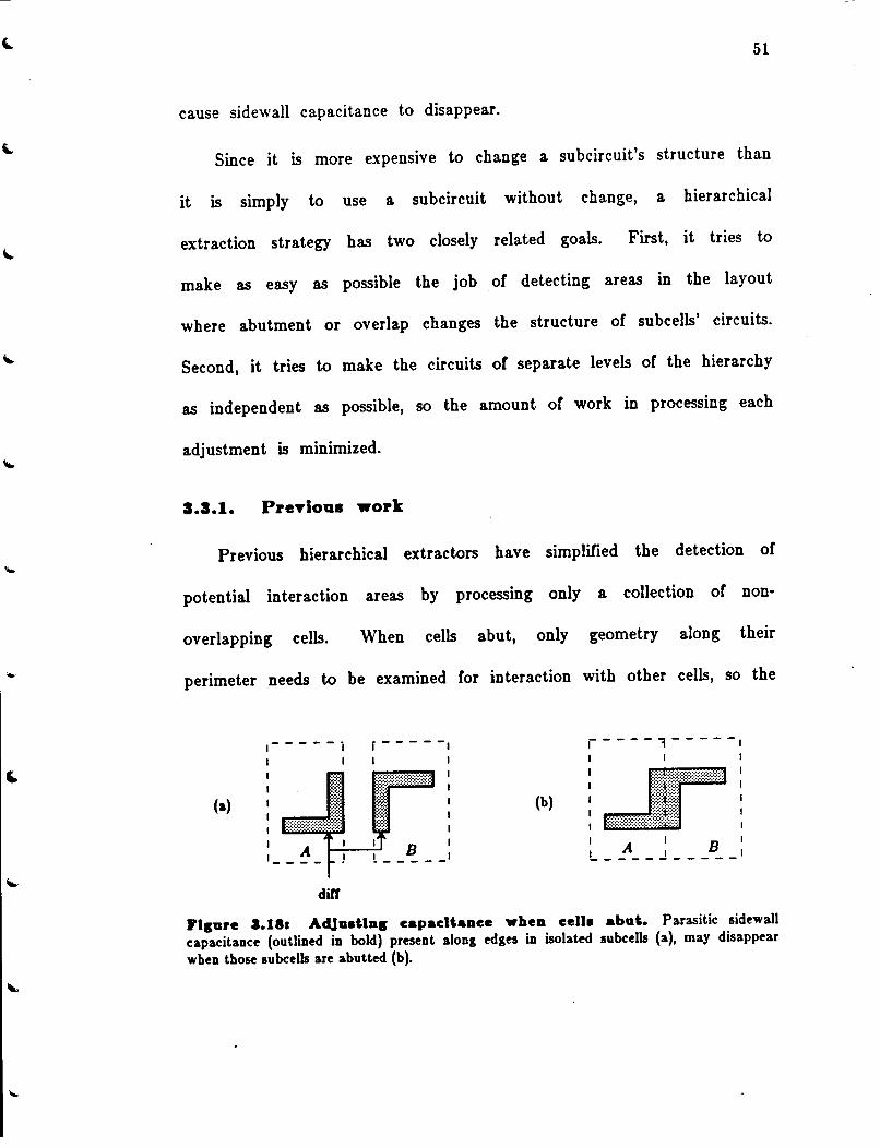
51
cause sidewall capacitance to disappear.
Since it is more expensive to change a subcircuit's structure than
it lS simply to use a subcircuit without change, a hierarchical
extraction strategy has two closely related goals. First, it tries to
make as easy as possible the job or detecting areas in the layout
where abutment or overlap changes the structure or subcells' circuits.
Second, it tries to make the circuits of separate levels or the hierarchy
as independent as possible, so the amount or work in processing each
adjustment is minimized.
a.a.l. PreTioua work
Previous hierarchical extractors have simplified the detection or
potential interaction areas by processing only a collection or non-
overlapping cells. When cells abut, only geometry along their
perimeter needs to be examined Cor interaction with other cells, so the
1----- 1 i----- r----1-----~
I I
(a) t:::=::::::::::::::::::::I-I-'-I-"-'Ifl'!'!!"""#"""::::::""":"""::::::"-"-':::1 I
--~- t ____ _
(b)
L __ A __ J __ _ B _ _
diff
l'lsure a.181 AdJudlas capacitance whea cell• abut. Parasitic sidewall
capacitance (outlined in bold) present along edges in isolated subcells (a), may disappear
when those subcells are abutted (b).

52
cost of hierarchical processmg IS proportional to the total perimeter of
abutting cells (Fit83]. In contrast, if cells are allowed to overlap,
potentially all of their interior geometry is subject to interaction.
The simplest approach, described by Scheffer (Sch81) and used m
(TaH83, Wag84), prohibits overlaps in the user's design. To allow cells
to be packed together as closely as possible without having to split
them into very small rectangular pieces, cells may have arbitrary
rectagonal borders. However, this approach often forces the designer
to partition a design in an unnatural fashion to avoid overlap.
Less restrictive approachs allow overlaps, but apply a disjoint
transformation before extraction in order to produce a collection of
unique, non-overlapping cells [NeF82, Whi80]. Each resulting cell
corresponds either to a cell with no overlaps, or to a unique
(a)
{c) .
PTITITil l.tilld
-. .
{b)
A+B
Flsu?e S.lth DlaJolnt, tranaform. The di1joint tran1/orm or !NeF82J converts a
collection or overlapping cella into a collection or disjoint (non-overlapping) ones. In this
example, the two cella A and B shown in (a) are overlapped with each other several times {b).
Only six or the combinations or overlapping cells are unique; these are shown in (c), and are
labelled in (d). The disjoint cella have arbitrary rectagonal boundaries.

-
53
combination of overlapping cells, as shown in the example in Figure
3.19. After the disjoint transform, the same procedures as used in the
first approach can be used to extract the disjoint cells. Unfortunately,
the disjoint transform results in a collection of cells whose structure no
longer parallels that or the original layout, so the resulting circuit
structure no longer has a cell-by-cell correspondence to the layout.
Both kinds or extractors process geometry along the perimeter or
subcells specially. Because only perimeter geometry is affected by
abutment, these extractors defer processing geometry at the perimeter
of subcells until the parent in which those subcells are used. For
example, IV (TaH83) only records sidewall capacitance in a subcell for
those edges that don't touch the subcell's boundary. Since geometry
along a subcell's boundary IS processed in the parent during
hierarchical extraction, sidewall capacitance due to such edges IS
recorded m the parent only if the edge has not disappeared as a
result of abutment with another edge. Fitzpatrick's extractor (Fit83)
and HEXT (GuH82) use a similar strategy for handling transistors:
they defer processing a transistor that touchs its cell boundary until
they visit a parent that wholly contains the transistor.
Incremental extraction using these extraction strategies has been
difficult for two rea.sOns. First, deferring the processing of geometry
along the perimeter of a cell means that a cell's circuit depends on

54
where it is located relative to the boundary of its parent cell. If the
original cell moves, then it must potentially be re-extracted.
A second problem occurs when using the disjoint transform. The
partitioning into disjoint cells depends on how cells overlap in the
layout. Moving cells in a parent can change the way it is broken up
into disjoint cells. As a result, all or the children or a cell may have
to be re-extracted when it changes.
S.S.2. Magie's strateu
Magic's hierarchical extraction strategy is unusual in two respects.
First, it allows overlap between cells, but does not use a disjoint
transform. Instead, it uses an algorithm that can process overlapping
cells directly, producing an output circuit with the same hierarchical
structure as the original layout. The overlaps it allows are only
slightly restricted: they may not make new transistors or destroy
existing ones. For example, polysilicon from one cell may not overlap
diffusion from another cell, since this would create a new transistor.
Second, the circuit for each subcell is complete, but is independent
of bow that subcell is used in the layout. Because the restrictions on
overlap ensure that no new transistors are formed, the connections and
adjustments that must be made each place a subcell is used are
strictly additive: merging of two nodes, changes to parasitic resistance
or capacitance of existing nodes, and addition of new coupling

li.. 55
capacitors. These additive adjustments are stored m each parent cell
that uses the subcell, without requmng that the subcell's circuit be
changed. As a result, only a cell and its ancestors must be re-
extracted when it changes; its children need not be.
Instead or brEaking up a layout into a collection or non-
overlapping cells wit.h a disjoint transform, Magic's extractor works by
finding interuction areas, and then finding the connections and additive
adjustments that must be made in each. Interaction areas occur
wherever geometry in two different subcells overlaps, or where mask
information in the parent cell overlaps a subcell, as shown in Figure
3.20. This approach is similar to that taken by several hierarchical
design-rule checkers, such as LYRA (Arn85) and the checker in Magic
[Ta084). In typical designs, such as the SOAR chip (UBF84],
metal---. cell A
·-- '"· I I I I
I I I I . - _, G-- ~
cell B cell
(a) (b)
Flsure 3.10a lateradloa are-. Only a small fraction of the total area of a cell
must be nattened durin& extraction. When two subcells abut or overlap (a), only the overlap
area (dotted lines) must be nattened. When mask &eometry from the parent overlaps a
subcell (b), the area of the subcell beneath overlappin& mask &eometry must be nattened.

56
interaction areas compnse less than 5% of the total chip area.
Processing interaction areas leads to a different style of algorithm
than abutment-only extraction. These abutment algorithms throw away
all but the geometry on the perimeter of subcells when processing the
parent, so the amount of geometry they must process is kept small
and they can run fast. In contrast, Magic doesn't throw away the
internal geometry of subcells. Instead, its overall speed comes from
the small size of interaction areas, and from the speed with which
corner-stitched tile planes can be searched.
3.3.3. Connections and adjustments
Processing each interaction area consists of making connections
between nodes and then making adjustments to parasitic resistance and
capacitance. Making connections is the easier of the two problems .
:rpl~ ~~: I
::::::::::::::::: I .:::::::::::::::::
I I
cell A
(a)
. 015pr
I, ............... I ··.············.·.··. I :::::::::::::;-:;: I
I ;::;: I
J., ::::: I ·l.fOPI ::::: I
I ::::: I I ..... I
cell B cell B
(b) (e)
Flsure 3.211 Area eapaeltanee adjudmenl. When subeells overlap, redundant
reporting or area capacitance must be eliminated. The polysilieon in cell A (a) has a total
capacitance or O.Ospr, while that in cell B (b) has a total capacitance or 0.06pf. When the
two cells overlap, as in (c), the total capacitance is the sum or that or cells A and B, minus
the capacitance or the overlap (0.015pl).

57
Whenever cells abut or overlap the extractor must check for material
from different cells that connects. When connections are detected,
additional information is added to the circuit of the parent to describe
the connections. Since making connections is a subset of the problem
of adjusting parasitic resistance and capacitance, it will not be
discussed further.
Section 3.3.1 has already shown how cell abutment can affect the
computation of perimeter capacitance. When cells are allowed to
overlap, area capacitance may need adjustment as well. Figure 3.21
shows that if two overlapping subcells both contain polysilicon m a
particular area, its substrate capacitance will be recorded twice, once
in each subcell. This must be compensated by a negative capacitance
in the parent cell. The total capacitance for each node is thus the
sum of the capacitances for that node in all cells, plus the negative
capacitance adjustments in all parents.
Internodal capacitance may also need to be adjusted· when subcells
overlap. If the material in cell B in Figure 3.21 were metal instead
of polysilicon, for example, overlapping the two cells would create
coupling capacitance in the area of the overlap.
In addition to capacitance, Magic also extracts resistance, which
may also need· adjustment when cells overlap or abut. Unfortunately,
resistance cannot be simply added or subtracted, as Figure 3.22 shows.

58
A
ltf~~t~fflt~~fJ~ A B
(a) B -lltt~~~~tt@If~~Itl
A B A B
(b) II-A A
(c) II- I B B
l'l11ure 3.22: Blerarehleal re.ldaaee adJuatmeat. When two wires abut as in
(a), the total wire resistance is the sum or the two resistances. When they abut as in (b), the
total resistance is hair. When overlapped as in (c), the total resistance is the same as each
resistance. Within an interaction area, however, it is often dirricult to distinguish between
these cases, since not all or the material or the two wires will be present. Instead of
computing a change in resistance, Magic computes the change in the perimeter and area or
the nodes in the subcells. After all changes to perimeter and area are known, the
approximation Cor resistance discussed in Section 3.2.3 can be used.
Instead, Magic records the change in perimeter and area of each node
resulting from a given overlap or abutment. Actual resistance of a
node is computed by applying all these adjustments to the perimeters
and areas in the subcells, and then usmg the approximation for
resistance described ID Section 3.2.3 with the adjusted perimeter and
area as input.
1.1.4. Extraction algorithm
Figure 3.21 shows an example circuit that contains two overlapping
subcells. A simple approach for detecting overlapping geometry is as

59
follows:
ADJUST!. For each tile t in the first subcell, search the area that it
covers in the second subcell for other tiles of the same
type.
ADJUST2. For each tile 8 found, compute the area of overlap between
8 and t. Subtract the area capacitance of this overlap
from the parent.
See Figure 3.23 for a detailed versiOn of the ADJUST algorithm.
When more than two subcells overlap, as shown in Figure 3.24,
additional care IS necessary to avoid counting overlaps more than once.
The area capacitance of two overlapping tiles is reported for each tile,
so the capacitance of one is correctly deducted by the ADJUST
Adjust( celll, ce112)
{
}
Cell •celll , •cell2;
lat area, cap; TUe "t, '\2; lled r;
lor ( ... each tile t. in celll ... ) {
}
lor ( ... each tile t2 in cell2 that overlaps t on the same plane ... )
{
}
r.r xbot- MAX(LEFT(t), LEFT(t2)); r.r:Jbot- MAX(BOTTOM(t), BOTTOM(t2)); r.r_xtop- MIN(RIGHT(t), RIGHT(t2)); r.r_ytop- MIN(TOP(t), TOP(t2)); area- (r.r_xtop- r.r xbot) •(r.r_ytop- r.r_ybot);
cap- area • AreaCaprfileType(t)); Adjust.Cap(NodeOf(t), cap);
Adjust
l'lsure 3.23: Alsorlthm ADJUST. This algorithm computes the adjustment to area
capacitance resulting from the overlap or two cella.

TTITi!!llll!ll.l!· ...................... . . . . . . . . . . . .. . . . . . . . . ..................... ................... . . .. . . . . . . . . . . . . . . . . . . . . . . . . . . . . . .. . ....................
A
················· ............ , .. , ••••••·o••"••••••••• ..................... .................... . . . . ' . . . . . . . . . . . . . .
:::::-:::::::·::·::::::: ..................... ····················· :: ~ ~ ~ ~ ~ ~.~ ~ ~ ~ ........ .
~1~t111rm~
B
lOpf
ABC
c
(overlapped)
adjustment == -60pf
computed - -30pf
60
rtsure 1.141 0Yerlap of more ihaa iwo •ubcell•. When tiles from three or
more subc:ells overlap, the ADJUST algorithm will compute too much adjustment. In this
example, cell A is overlapped by cells Band C. The capacitance in the area or the overlap is
lOpf. Ir the ADJUST algorithm were run on all three cells, it would compute 20pf
adjustment for A, and the same amount for B and Co This is a total adjustment or 60pf,
more than the sum or the individual capacitances in the overlap area {30pf), resulting in a
negative adjusted capacitance.
algorithm. However, when three tiles overlap, the capacitance of the
first should only be deducted once. Unfortunately, the ADnJST
algorithm above deducts capacitance for each overlapping tile, rather
than only Cor the first overlap.ping tile.
To prevent excessive deductions, Magic uses a cumulative buffer.
Initially, this buffer is empty. Processing a subcell consists of checking
Cor overlaps between the subcell and the cumulative buffer, then
copying the subcell into the cumulative buffer and merging with any
geometry already present in it. After each iteration, the cumulative
buffer contains the geometry of all cells processed up to that point.

c..
,
61
Because geometry in the cumulative buffer is merged, even if two
previously processed cells had a tile in the same area, there will be
only one tile in the cumulative buffer. Hence, there will be only one
adjustment to capacitance. The algorithm _with the cumulative buffer
is as follows:
CUMULATIVE!. Begin with an empty cumulative buffer.
CUMULATIVE2. Process a subcell. For each tile t in the subcell,
search the area that it covers in the cumulative
buffer for other tiles or the same type.
CUMULA TIVE3. For each tile 8 found, compute the area of overlap
between 8 and t. Subtract the area capacitance of
this overlap from the parent.
CUMULA TIVE4. Copy the geometry from the su bcell being processed
into the cumulativ.e buffer.
CUMULATIVES. Go to CUMULATIVE2 if subcells remain; otherwise,
stop.
See Figure 3.25 for details of the CUMULATIVE algorithm.
When the subcells themselves have children, a logical extension of
the above procedure would be to search for all tiles in all cells in the
first subtree, and check for overlaps with all tiles m all cells in the
second subtree. Unfortunately, this fails when tiles m two children of
the same subcell already overlap, as shown in Figure 3.26. The
capacitance adjustment due to the overlap has already been computed
when the subcell was extracted, and should not be computed agam m
the parent.

Cumulative{ area) a-t ~rea;
{
}
Cell •cum, •cell; lat area, eap; TUe ~.-a; lleetr;
cum - NewCell(); lor ( ... each cell overlappinr; area ... ) {
}
lor ( ... each tile t. in cell ... ) {
}
lor ( ... each overlappinr; tile 1 in cum, or same type as t ... )
{
}
r.r_xbot- MAX(LEFT(t), LEFT(s)); r.r_ybot- MAX(BOTTOM(t), BOTTOM(s)); r.r_xtop- MIN(RIGHT(t), RIGHT(s)); r.r_ytop- MIN(TOP(t), TOP(s)); area- (r.r_xtop- r.r xbot) *(r.r_ytop- r.r_ybot); eap -area • AreaCapffileType(t)); AdjustCap(NodeOC(t), eap);
;• Merge cell with cumulative h//er r Merr;eCell( cell, cum);
62
Cumulative
Flsure a.JSa AlsorlthJD CUMULATIVE. This algorithm accepts as input an area,
and processes adjustments to capacitance ror each cell that overlaps that area.

63
child!
Ftsure 3.21: Compen•a~lon for multiple oYerlap•. Two tiles in two different
subcells (child 1 and child 2} of cell A overlap. The circuit for cell A contains the capacitance
compensation due to this overlap. When the parent is extracted, we don't want to
compensate ror the overlap or childl and child2 a second time. However, cell B overlaps
cell A, so we still must compensate once ror the overlap or cell B and the geometry in cell A.
The problem is that overlaps within subtrees have already been
compensated (or. The parent should compensate only (or overlaps
between subtrees. Magic ensures this by combining (flattening) all the
geometry in a subtree into a single set or tile planes. As a result,
there is a single tile Cor each area where geometry appears in any oC
the cells in that tree. In effect, flattening each subtree reduces the
problem to that originally considered, when each subtree was only a
single level deep.
The same considerations that apply to area capacitance
adjustments (rom overlap also apply to perimeter capacitance
adjustments (rom abutment. Instead or searching Cor overlaps between
tiles, the extractor searches to see whether each tile edge m one
flattened subtree abuts or overlaps any tiles m any other flattened

64
subtrt!es. Whenever such abutment or overlap IS detected, the
perimeter capacitance due to the edge is deducted from the parent.
If Magic disallowed cell overlaps, and instead only allowed
abutment, it would not be necessary to flatten each subtree. Tiles
from different cells could never overlap, so only perimeter capacitance
would need to be adjusted. At most two non-overlapping tiles could
share a single segment of boundary, so there would always be a
unique place in the hierarchy where that boundary's capacitance would
be updated.
In the algorithm just described, it might appear that every subtree
of a parent must be flattened, and each flattened tile be checked
against every other flattened treeo II this were truly the case,
hierarchical extraction would be at least as expensive as fiat extraction,
since the entire circuit would be flattened when the root cell m the
design was extracted. Fortunately, this processing is limited to the
portion of each subcell that overlaps the interaction area being
processed, which generally accounts for less than 5% of the total area
of layouts.
a.a.&. Arra7s
The amount of work the extractor must do is greatly reduced by
taking advantage of explicit arrays. These are represented in Magic
by a single subcell that is marked as being replicated into a one- or

65
(1,41 (2,41 (3,41 (4,41
(1,31 (2,31 (3,31 (4,31
-- _l)t I Vl -- -~ -~ ~
I ~ (2,21 (3,2J (4,21 (1,214f ..... -~ ~
If'.
-,"'-(1,11 (2,11 (3,11 (4,11
Flsure 3.27a ArraJ'•• All possible connections and overlaps between overlapping array
elements are identical to the ones that occur in the shaded area. These interactions are
between the element in bold ((1,21} and ita neighbors indicated by the arrows. For example,
interactions between array element (1,2J and element (2,2J, are the same as those between
element (2,21 and (3,2J, and between (3,21 and (4,2J.
twcrdimensional array of identical elements. The subcell IS also
marked with the separation between successive elements in the array.
Adjacent elements may overlap.
Magic's extractor exploits the fact that all elements in an array
are identical. For example, m an array of N elements in the x-
direction, the connections between an element and its right-hand
neighbor are the same for elements 1 up through N-1. Similar
statements apply in the y-direction and along the two diagonals. As a
result, Magic only extracts the interactions in the canonical areas
shown in Figure 3.27, and then iterates these interactions over all
applicable elements in the array without having to do any additional

66
work of extraction. This iteration has a compact form in the
extracted file, with the range of indices specified explicitly whenever a
connection or adjustment between elements of an array is made. For
example,
merge A[l:3,1:4)/in A(2:4,1:4]/out
is output to show connections between elements A[l,l)/in and
A(2,1]/out, elements A[1,2)/in and A[2,2)/out, etc.
a.a.e. Node names
Magic uses hierarchical names to refer to nodes in subcells. The
name of a node in a subcell consists or a path of cell instance
identifiers from the root all the way down to the subcell, followed by
the node name from the subcell. For example, if the root cell
contains cellA, cellA contains cellB, and cellB contains a node x, its
full name is cellAjcellBjx. As mentioned in the description of the
basic extractor, the nodename can either come from a label attached
to geometry in that node, or it can be generated automatically if no
labels are attached to it. When connections between nodes in subcells
are reported in a parent cell, the nodes are named with their
hierarchical paths, relative to that parent.
In order for incremental extraction to work efficiently, it must be
possible to find the name of a node in a subcell without having to
...
67
re-extract the subcell. If the subcell's node is labelled inside the
interaction area being flattened by the hierarchical extractor, that label
will remain attached to the node in the flattened subtree. The node
name is just this label, prefixed with the hierarchical path down to
the subcell.
When no label is attached to a node in the flattened subtree,
Magic must find the subtree from which the node came and extract
just that one node. The flooding algorithm used by the flat extractor
comes in handy here. Given the location of one point in a node,
flooding lets you extract only that node without paying the price of
extracting all other nodes in a cell.
If a label cannot be found for the node outside the flattened
area, the node name must be generated automatically. It is critical
that this name be identical to the name generated when the subcell
was extracted.
The simplest generated node name would be a umque integer .
Node numbers could start at zero and be incremented by one for each
new new node found during basic extraction. Unfortunately, with this
scheme it is impossible to determine a node's number without
extracting all other nodes in the cell. To allow the hierarchical
extractor to generate the name of a single node in a subcell without
performing a complete extraction of the cell, Magic uses a different

68
approach.
Because tiles cover a corner-stitched plane completely and with no
overlaps, each point in a plane belongs to exactly one tile. On a
given plane, then, the points m the tiles belonging to one node do
not appear in any other node. Magic therefore chooses the point in a
node with the smallest X coordinate from among the points with the
lowest Y coordinate that belong to the tiles in a node. Because tiles
in different planes can overlap, this (X,Y) point IS chosen from the
lowest-numbered plane P on which there are tiles for a node, and
used to generate the unique node name (X,Y,P).
3.4.. Incremental extraction
The strategy described in the previous section guarantees that
when a cell changes, its subcells need not be re-extracted. However,
A X ...... : ... / ~ ...
cht~nged
. . . . . . . . . . . . . . . . \ ..... · :. ..... · \ ••••• !
Flsure 1.181 Jacremeatal exbadloa. When one cell in the layout changes, only its
ancestors must be re-extracted. The re-extracted cells are shown in bold above.

69
its parents will need to be re-extracted because the overlaps or
connections between the cell and its parent may have changed. This
process continues upwards through the hierarchy until the root 1s
reached, as shown in Figure 3.28. As a result, the root will need to
be re-extracted whenever any part of the layout changes.
Magic already keeps track of when cells have changed, for
purposes of design-rule checking. The file that holds a cell's layout
contains a timestamp of when that cell was last modified. The
Wlthoa~ coapllas capacl~aace
Fetsfaec
Design min max mean
SOAR 6 122 66
EX1 30 88 68
EX2 41 68 54
SPUR 14 74 53
TRC 5 102 52
Wl~h coupllas capacl~aace
Fets/sec
Design min max mean
SOAR 2 57 32
EX1 21 66 43
EX2 31 41 34
SPUR 9 47 33
TRC 5 89 45
Table 3.11 Fla~ e:dradloa performaace. This table lists average, minimum, and
maximum nat extraction speeds on a V AX-11/780 ror all the cells in several designs. The
speeds in the first part or the table include extraction or coupling capacitance; those in the
second part include only substrate capacitance. SOAR is a 37,700-transistor microprocessor.
EX1 is a 2,000-transistor chip, provided courtesy or Richard Kenner at NYU. Both are
designed in single-layer nMOS. EX2 is a 7 ,200-transistor CMOS design, also rrom Richard
Kenner. SPUR is a 10,000-transistor chip consisting mainly or a datapath, also designed in
two-layer CMOS. TRC is also a 10,000-transistor chip in two-layer CMOS, provided by Bill
Dally and Chuck Seitz or Caltech.

70
extracted circuit for each cell contains a copy of the layout's
timestamp at the time of the last extraction. To determine when a
cell must be re-extracted, Magic compares the timestamps of its layout
and its extracted circuit. If they differ, that cell and all its ancestors,
recursively back to the root, are marked for re-extraction.
a.5. Performance
The fiat extractor processes 50-65 fets per second (on a V .AX-
11/780 runnmg Berkeley Unix), if only resistance and substrate
capacitance are being extracted. When coupling capacitance is
extracted as well, the fiat extractor processes 25-35 fets per second.
Table 3.1 reports the distribution of fiat extraction speeds for all the
cells in several different designs. Table 3.2 compares these speeds
with several other systems.
The real measure of the extractor's performance is how fast it can
extract complete hierarchical layouts. Table 3.3 gives the time it
takes to perform a complete hierarchical extraction of several designs.
On average, Magic's hierarchical speed is comparable with that of its
nat extractor.
There are both advantages and disadvantages of hierarchical
extraction. When large arrays are present, as in the register file
example in Table 3.4, hierarchical extraction is considerably faster than

"
71
System Fets/second
IV [TaH83J 1-2
MEXTRA [Fit82J 6-10
ACE [Gup83j 8-14
Magic (with coupling) 25-35
Magic (no coupling) 50-65
Table 1.2: Comparlaon wUh other ftat extraetora. Speeds are in transistors
per second on a V AX-11/780. The extractors differ slightly in the amount of information
they compute: all but ACE compute capacitance to substrate, and only IV and Magic
compute coupling capacitances. The functions used to compute capacitance from perimeter
and area are essentially identical for all extractors that perform this computation. Only
Magic computes resistances, although ACE and MEXTRA provide the same perimeter and
area infornaatio11 used by Magic in its resistance approximation. The MEXTRA, ACE, and
Magic times are for Manhattan layouts. The numbers for Magic: give the speed both with
and witho~t the computation of coupling capacitances. Performance figures for all other
extractors come from the indicated reference.
Design Time Fets Fets/sec
Regfile 0:02 6,Q12 3456
EX2 0:31 7,200 228
SOAR [UBF84] 15:22 37,000 40
SPUR 3:31 Q,Q50 47
EXI 1:24 2,034 24
TRC 3:23 10,000 4Q
Table 1.4: Blerarehleal extraction tlmea. This table gives hierarchical extraction
times (minutes:seconds on a V AX-11/780) for several hierarchical designs. They show that in
some cases, hierarchical extraction results in a significant speedup: Regfile is a 36x32 bit
register file array that is easy to extract because of its regularity. EX2 is a complete chip
with a very regular central array. More typical of hierarchical extraction speeds are the
remaining examples. The fets columns measures the number of transistors if the hierarchical
design were fully instantiated, as would be required by a non-hierarchical extractor.
fiat extraction. The speed or array extraction comes from having to
extract the same amount or information regardless or the size or the
array.
A disadvantage or hierarchical extraction is its overhead, which is
greater than that or fiat extraction. Figure 3.2Q shows that the
benefits of array extraction become apparent only for arrays with more

72
than a few elements m them.
While Magic is very fast at extracting a complete design, it is
even faster if it only has to extract part or one. This 1s the
advantage of incremental, hierarchical extraction. Table 3.5 shows the
times required for incremental re-extraction of the several designs.
s • celll ---nat
• cell2 ··············· array
• cell3
3
Time
2 ... .. . ··
1 -•·······•·······•······ .. ······•······•······•
ol-~·~-=--·;··=··:··-~-·~·::;:~·~-:···:··;•:···:··~··;·:···::*;· __ ~ 0 1 2 3 4 s 6 7 8 0
Number Array Elements
Flsure 3.21: Arra7 extradloa performaaee. The overhead of array extraction is
sutriciently higher than that of nat extraction to offset any speed benefits unless the array
contains more than a minimum number of elements. Each example has two lines: the solid
line is the time to extract the array alter nattening it, and the dotted line is the time to
extract the array by taking advantage of the array structure. All cells were arrayed by
horizontal abutment. The cells used are described in the following table (width and height
are in lambda). All were NMOS.
Name Celll CeU2 Cell3
Fets 16 24 3
Width 107 48 21
Height 48 02 2S

73
Incremental re-extraction time
Design Fets min max mean Complete extraction
SPUR 9,950 0:41 1:09 0:57 3:44
SOAR 37,000 4:00 7:55 5:20 15:22
EX1 2,034 0:11 1:16 0:46 1:24
EX2 7,200 0:28 0:30 0:29 0:31
TRC 10,000 0:39 1:15 0:58 3:23
Table J.&a Incremental re-extradlon tlmea. Times (minutes:seconds on a VAX-
11/780) to perform incremental re-extraction or the designs listed in the previous table. Tbe
incremental time is that required to re-extract tbe design after one or tbe cells bas changed;
tbe min, max, and mean are taken across all cells in a given design. Tbe right-band column
gives tbe time required for a complete re-extraction.
The typical speedup due to incremental extraction lS a factor of 4 or
5 over a complete re-extraction.
3.1. Limitations and further work
Although the extractor has been used successfully on a number of
large designs, a few problem areas still remain. This section discusses
four of these, and suggests areas for further work.
1 MH~~~~~~~~~~~~~~~~~~~tt~~~~~~~~~~~lt~~t~~~~~~~~~~~~~~~~~~~~~~t~~t~~H~~~~~~tt~~~~~~~~~~~t~~~~~~~~~=i~~~~~t~f:~h
2
Flsure J.JO: Realatanee In multi-terminal node•. Each node has a single
resistance associated with it. When there are multiple connections to the node, any shorter
paths (e.&, between 1 and 2) are billed the same amount or resistance as the longest path
through the node (between 1 and 3).

74
3.1.1. Resistance
In the node model, each node in the layout has just a single
value of resistance associated with it. All paths between transistors
connected to this node are assumed to incur the cost of passing
through this resistance. While this model is valid for nodes with only
two terminals, it can lead to overestimation of resistance when a node
connects to several devices. For example, in Figure 3.30, the paths
between some of the connections do not pass through the full length
of the node, but the node model nonetheless treats them as having
the full node resistance. In the worst case, immediately adjacent
connections on a bus-which should have nearly zero resistance
between them-can be billed the resistance or the entire bus from one
end to the other.
A more serious problem results from the way in which Magic
computes resistance from perimeter and area. Figure 3.31 shows how
1 >:·:·:·:·:·:·:···:·:·.···:;:
(a) ~ .·· ~ :~ ·=-··················· ·.·.-.... )$f
Flsure 3.311 Re•l.taoee lo braoehlos oode•. Using perimeter and area to
approximate resistance doesn't always work. Both (a) and (b) have the same perimeter and
area, so the computed resistance for both will be the same. However, the actual resistance
between points 1 and 2 in (b) is significantly less than that between 1 and 2 in (a}.

75
this approximation overestimates the resistance or a node with many
side branches. This problem is particularly noticeable in the case or a
large central metal bus with many high-resistance polysilicon side paths.
The actual resistance from the bus through a poly path is errectively
just the resistance or a single poly path (metal resistance is negligible),
but Magic computes the resistance to be the sum or all the poly
paths, a serious overestimation.
Several solutions are possible. The first 1s to identify points
where a node branches, and break the original node up into smaller
nodes. A useful choice or branch points would be contacts between
Flsure 3.31a Node apllUlas. One way oC increasing the accuracy or resistance
estimation, while still preserving the notion or nodes, is to treat interconnecting material as
one or more nodes connected by resistors. In this example, nodel and node2 correspond to
the left and right halves or the metal bus, while node3 corresponds to the high resistance poly
feeder. This approach bas the compactness or the node approach as long as explicit resistors
are used infrequently.

76
material of low resistance (e.g, metal) and high resistance (e.g,
polysilicon or diffusion); this would handle the poly feeder problem
discussed above. This approach requires extending· the node model to
include the idea that nodes might be connected directly to other nodes
through explicit two-terminal resistors. See Figure 3.32 for an
example. As such, it would require making changes to the vanous
simulation programs that accept a node and transistor description as
their input.
An alternate solution would not modify the node structure, but
instead compute a better approximation for the resistance of a node.
By identifying the direction of current now in a wire-e.g.,
approximating it by the long direction-the extractor could compute
the resistance of each path between a pair of devices through the
node separately, and then use the average of the values so obtained.
This would not solve the problem of multi-terminal nodes with varying
resistances for their internal paths, but it would reduce the error
introduced for branching nodes by the perimeter/area approximation.
3.1.2. MassiTe OTerlaps
When two cells overlap each other in their entirety, hierarchical
extraction is more expensive than first flattening both cells and then
using the nat extractor to extract them. This problem is particularly
severe when it occurs at the level of a fioorplan. Table 3.32 shows

'""'
77
Incremental re-extraction time
Design min max mean Complete extraction
SOAR-Oat 4:00 7:55 5:20 15:22
SOAR-overlap 7:01 11:06 8:23 20:02
Table 3.81 Etfeet of o"Yerlap oa e:dradloa time. Times (minutes:seconds on a
V AX-11/780) to perform incremental re-extraction of two different versions or the SOAR
chip. The global routing in SOAR-Oat is contained in the root cell, while that in SOAR
overlap is contained in several subcells that overlap much or the rest or the design. The
additional time for re-extraction of SOAR-overlap comes from the extra hierarchical
processing caused by this massive overlap.
one example where placing the global routing into several overlapping
cells instead or m a single cell can make a 30% difference in
extraction speed.
Since it is easy to detect when massive overlap exists, one
approach might be simply to flatten such cells, extract them using the
fiat extractor, and output information in the extracted file that says to
ignore any information from subcells. Perhaps the best approach,
though, IS simply to make designers aware of the cost of massive
overlap, and to encourage them to design cells to abut or overlap only
near their boundaries.
a.a.s. lnc:remental extrac:tion
Whenever a cell in the layout changes, Magic's incremental
extractor causes all or its ancestors to be re-extracted. Unfortunately,
nearly all the time or incremental extraction is spent re-extracting
these ancestors. The root cell alone accounts for 50-60% or the cost
or incremental re-extraction in the SOAR chip.
78
Under some circumstances, it might be possible to avoid having to
re-extract all of a cell's ancestors. For example, if only internal
geometry in a subcell were changed, in such a way as neither to
make nor break connections with its parents, then it should not be
necessary to re-extract the parents. By recording the areas that have
been modified as a result of editing operations, in much the same way
as is done for Magic's design-rule checker [Ta084), it should be
possible to detect when the parents needn't be re-extracted.
A potential problem with this idea is that connections in the
extracted circuit file are made by name, not by geometry. Hence,
even if connections to a parent were neither made nor broken, a
change to a subcell that caused node names to change would force the
parents to be re-extracted so their connections could refer to the new
node name. Such a change could result if a label attached to
geometry in a node were removed, or if a node with an attached
label were split into two pieces, with the label remaining attached to
a different part of the node than that connected to by a parent.
Finally, since some node names are generated automatically based on
the lower-left corner of the geometry in a node, any change to this
location would force re-extraction of parents. The additional overhead
or keeping track of these changes may make the net payoff of this
strategy minimal.

7Q
3.1.4. J..femory requirements
A potential disadvantage or using corner-stitching as the basis or a
circuit extractor is that it requires each cell to be memory resident.
However, because most cells in hierarchical designs tend to be small
[OuU82], this should not be too much or a problem; the number or
pages or memory required to hold each cell while it is being extracted
is fairly small. Even the space required to represent an entire layout
m memory is not excessive; the 36,000 transistor SOAR chip occupies
6.1 megabytes when completely loaded, and the resident-set size during
extraction is on the order or 2.5 megabytes.

80
Chapter 4
Plow ins
Custom VLSI layouts are difficult to modify. Because of this,
designers are often committed to the initial choice of implementation,
rather than being able to experiment with alternatives. Existing cells
often cannot be re-used in subsequent designs because they don't quite
fit; it is typically easier to redesign a new cell from scratch than to
modify an old one. Bugs in a dense layout are hard to fix, leading
to a debugging cycle that can take days or weeks.
Many of these difficulties stem from the fact that seemingly small
changes to a layout can have disproportionately large effects. As
(a) (b)
Figure 4.1a Small ehause• eau haYe larse etfeda. Opening up new space in a
layout can cause effects that ripple outward over a much larger area. Creating enough space
to increase the size or the box B in (a) requires moving all the tightly packed bars above,
below, and to the right orB, and their neighbors, and so forth until empty space is reached.

'
81
Figure 4.1 illustrates, merely openmg up new space m a layout can
cause effects that ripple outward over a much larger area. These
effects occur because area lS at a premium, so cells are designed with
little room to spare. When anything in the cell moves or gets bigger,
its neighboring information must be moved as well in order to ensure
that layout rules-minimum widths and spacings-are satisfied. Simply
stretching an entire cell is usually an inefficient way to open up new
space.
Past approaches to improving layout modifiability have
concentrated on providing the designer with an easy-to-edit
representation that lS independent of the complex width and spacing
rules required for physical mask layout
[BMS81, da84, LNS82, RBD83, Wes81a, Wil78). When ready to fabricate
the circuit, the designer invokes a compactor to convert the user
representation into a dense physical layout
[Bal82,Hsu7Q,Kin84,LeM84,LiW83,MNE82,Mos81, ZDC83]. Section 4.1
reviews these approaches and discusses their limitations.
Plowing, introduced in Section 4.2, offers a different solution: it
makes it easy to perform complex manipulations, like the one in
Figure 4.1, directly on mask layout. This makes it unnecessary for
designers to work with two different representations for the same
design. With plowing, a designer can move one or more pieces of

82
geometry, with the plow opereration stretching or compacting other
geometry as needed to preserve the circuit's connectivity and layout
rule correctness.
The next three sections focus on the implementation of plowing.
Section 4.3 presents the essential components of the plowing algorithm.
This algorithm relies heavily on the ability to perform several different
kinds of geometric searches efficiently; Section 4.4 presents algorithms
based on corner-stitching to do so. Finally, Section 4.5 describes a
number of extensions to the algorithm of Section 4.3 that improve the
usability of plowing.
Section 4.6 evaluates plowing, both as a compactor, and as a
method of quickly making changes in a layout. Section 4.7 concludes
by discussing plowing's limitations and areas for further work.
4.1. Previous work
Previous systems have addressed the problem of layout
modifiability by isolating the user from details of component sizes and
spacmgs. To do this, they work in two phases. In the first phase,
the user edits a representation of the design, usually one in which the
approximate sizes and relationships of components are present, but with
no explicit physical dimensions. Two styles of representation for this
phase have been popular: symbolic, and procedural/textual.
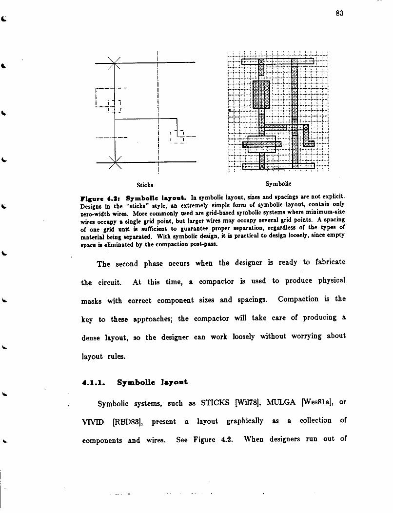
83
Sticks Symbolic
Flsure 4.1: S,-mbolle la,-out. In symbolic layout, sizes and spacings are not explicit.
Designs in the "sticks" style, an extremely simple form or symbolic layout, contain only
zero-width wires. More commonly used are grid-based symbolic systems where minimum-size
wires occupy a single grid point, but larger wires may occupy several grid points. A spacing
or one grid unit is surricient to guarantee proper separation, regardless or the types or
material being separated. With symbolic design, it is practical to design loosely, since empty
space is eliminated by the compaction post-pass.
The second phase occurs when the designer is ready to fabricate
the circuit. At this time, a compactor is used to produce physical
masks with correct component sizes and spacings. Compaction is the
key to these approaches; the compactor will take care of producing a
dense layout, so the designer can work loosely without worrying about
layout rules.
4.1.1.
Symbolic systems, such as STICKS (Wil78], :MULGA (Wes81a], or
VIVID (RBD83], present a layout graphically as a collection of
components and wires. See Figure 4.2. When designers run out of

84
space m the middle of a layout, these systems allow them to stretch
the layout by inserting additional grid lines, as shown in Figure 4.3.
Even though this may be wasteful of space in the symbolic design,
any unnecessary space should be eliminated by the compactor when
masks are generated.
4.1.2. Procedural/textual la7out
In procedural or textual systems, layout is generated from a
textual description. This description has many of the characteristics of
symbolic layouts: it IS usually metric free, specifying relative
placements, as in the PLATES system (SaK82}, and it may incorporate
parameters and procedures as in ALI [LNS82), ALLENDE (da84), or
added grid linea -
(a) (b) (c)
l"laure 4.3a Openlna up new •paee In a •7mbolle la7out. To open up new
space in a symbolic layout (a), it is merely necessary to stretch the cell by inserting new grid
lines at the point where more space is required (b). Once more space is available, it is easy
to add new geometry (c).

85
the HILL system [LeM84]. Physical layout is generated by solving a
system of constraints that include layout-rule widths and spacings in
addition to the relative placements specified by the user, in much the
same way that a compactor generates layout from a symbolic
description.
These systems have an advantage over symbolic or mask editing
systems in that they are easily parameterizable. If a designer plans
on making certain kinds of changes from the start, such as increasing
power, changing clocking, etc., then the design can be parameterized
to allow them. To implement the change, the designer need merely
change a parameter, instead of having to make each such change
manually. Unfortunately, parameterizability doesn't make designs any
easier to enter in the first place, nor it is useful when debugging a
design. Bugs are usually unexpected, so it is unlikely that they can
be rl.Xed simply by tweaking parameters. Textual designs generally
take longer to debug than those drawn with a graphics editor [Tri81].
Usually several iterations of writing a procedural description, followed
by generating a layout and v1ewmg it graphically, are required before
the designer is satisfied with the result.
4.1.3. Compaetloa
All of the above approaches rely on some Corm of compactor to
convert the user's representation of a design into a dense physical
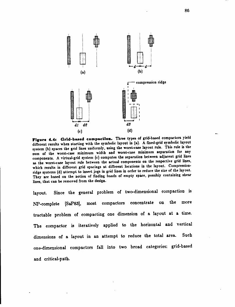
w .
.
.
(a)
• . . .
m w ... dl d!!
(c)
• .
.
... =~· :· . :: •'
. , ~ . w · .
.
• . .
.
;...__ d___.;_ d~
(b)
r- compression ridge
:dlb I~ I . --:--1
ruw: :,...._,.; I
d9
(d)
86
Flsure 4.4: Grid-baaed eompadloa. Three types or &rid-based compactors yield
different results when starting with the symbolic layout in (a). A faxed-grid symbolic layout
system (b) spaces the &rid lines uniformly, using the worst-case layout rule. This rule is the
sum or the worst-case minimum width and worst-case minimum separation for any
components. A virtual-grid system (c) computes the separation between adjacent grid lines
as the worst-case layout rule between the actual components on the respective grid lines,
which results in different grid spacings at different locations in the layout. Compression
ridge systems (d) attempt to insert jogs in grid lines in order to reduce the size or the layout.
They are based on the notion of finding bands of empty space, possibly containing shear
lines, that can be removed from the design.
layout. Since the general problem of two-dimensional compaction is
NP-complete (SaP83), most compactors concentrate on the more
tractable problem of compacting one dimension of a layout at a time.
The compactor is iteratively applied to the horizontal and vertical
dimensions of a layout in an attempt to reduce the total area. Such
one-dimensional compactors fall into two broad categories: grid-based
and critical-path.

87
4.1.4. Grid-based eompaetora
Grid-based compactors map the user's design onto a grid, eliminate
empty grid lines, and finally select spacings between the remaining
lines sufficient to satisfy the layout rules. Figure 4.4 gives examples
of several grid-based compaction strategies.
The earliest such compactors [GiN77,Lar7l,Lar78} used a fixed
grid. After eliminating empty grid lines, the remaining lines were
spaced uniformly by the worst-case layout rule. Virtual-grid
compactors such as 1D MULGA [Wes8la} or VIVID [RBD83} produce
denser layouts by spacing each pair of grid lines by the worst-case
layout rule between components in the two lines, rather than the
overall worst-case rule. These grid-based compactors have generally
good performance, with runtimes linear in the number of components
being compacted [BoW83}.
Both fixed-grid and virtual-grid approaches requue all objects on
the same grid line to move · together as a unit during compaction,
even if the design rules would permit some components to move closer
than others. This inability to shear limits the density of the resulting
layout, so designers usually compensate by placing objects on staggered
grid lines. This improve5 the quality of the resulting layout but
complicates the symbolic design.
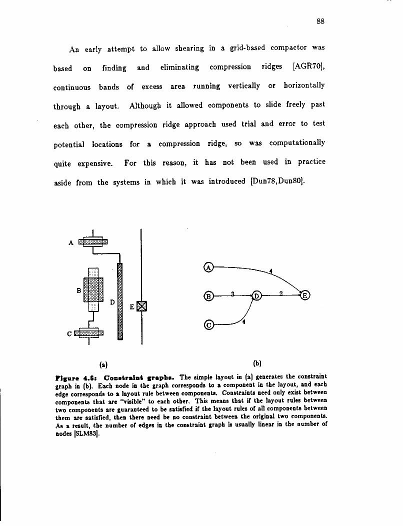
88
An early attempt to allow shearing m a grid-based compactor was
based on finding and eliminating compressiOn ridges [AGR70],
continuous bands of excess area running vertically or horizontally
through a layout. Although it allowed components to slide freely past
each other, the compression ridge approach used trial and error to test
potential locations for a compression ridge, so was computationally
quite expensive. For this reason, it has not been used in practice
aside from the systems in which it was introduced [Dun78,Dun80].
A
D E
(a) (b)
l'lsure 4.&c Cou.tralut sraph•. The simple layout in (a) generates the constraint
graph in (b). Each node in the graph corresponds to a component in the layout, and each
edge corresponds to a layout rule between components. Constraints need only exist between
components that are "visible" to each other. This means that if the layout rules between
two components are guaranteed to be satisfied if the layout rules or all components between
them are satisfied, then there need be no constraint between the original two components.
As a result, the number or edges in the constraint graph is usually linear in the number or
nodes jSLM83).

4.1.5. Critical-path compactors
The other maJor approach to compaction is critical-path
compaction, such as used in CABBAGE (Hsu7Q,MNE82), and other
systems (Bal82,Kin84,LiW83,Mos81, ZDC83). It works by converting the
compaction problem into the problem of finding the longest path in a
constraint graph that represents the minimum spacing requirements
between circuit components. Each node in the graph corresponds to a
component, and each edge corresponds to a minimum-separation
layout-rule between them, as shown m Figure 4.5. A variety of
linear-time algorithms (The78, Chapter V) may then be used to find
the critical path in this graph. Once the critical path is known, the
location of all the components on the path can be determined, and all
other geometry positioned relative to them.
Constructing the constraint graph involves creating an edge for
each layout rule that applies between a pau of components. In the
worst case, this graph might contain an edge between each node and
every other, for O(_N'2) edges given N components. Usually, however,
constraints are only required between adjacent components, so the
graph is planar and the number of edges is O(N). Efficient solutions
exist to construct this graph in time O(N logN) (DoL85,SLM83). The
plowing algorithm described later in this chapter is like a critical-path
compactor that operates directly on the layout, but without the

go
intermediate step of constructing an explicit constraint graph.
4.1.1. Shearing and Jogs
Critical path compaction offers an advantage over grid-based
algorithms by allowing shearing. Vertically aligned but unconnected
components are assigned to their own independently movable nodes,
unlike the components on a grid-line which must move together.
However, even greater density is possible if a compactor can
introduce jogs to allow pieces of a wire to move independently, as
shown in Figure 4.6. Several systems have used heuristics to find
suitable jog points. Watanabe's compactor (W at84} and CABBAGE
[Hsu7Q} both identified wires with a high "torque" as candidates for
jog insertion. The critical path enters such wires from a component
near their top and exits through a component near their bottom, or
I I ~~~:0000
0 0
I 0
fli'-l ~
L--------..,.---J
(a)
I
I~~ I
I R'-11 liCiil
I
'--------·
(b)
-----· (c)
Flsure 4.11 Jos lat.rodudlon. The central wire prevents the the cell in (a) rrom
being compacted any more than (b) ir no jogs are introduced. Ir the wire can be bent in the
middle by the introduction or a jog, a denser layout is possible (c).

'
Ql
vice-versa. Wolf's Supercompaction [Wol84) also considers introducing
jogs in a direction perpendicular to that being compacted, by searching
for certain patterns of wires and breaking them up into segments
according to a set of rules.
A problem with these heuristic approaches is that they need to
know the locations of jog points in order to build the constraint
graph. Once the constraint graph is built, they can't further fragment
nodes in the graph to introduce new jogs. The only way for such
approaches to be certain to introduce all necessary jogs would be to
create a separate node for each minimum-size component or segment of
wire in the layout, in effect introducing potential jogs at all possible
positions in the layout. Unfortunately, this approach can require
exponential time on some inputs, and in general can be expected to
be computationally expensive (Mal85). As I shall discuss later, plowing
overcomes this difficulty by avoiding an explicit constraint graph, and
being able both to detect points for jog introduction and to introduce
jogs as it proceeds.
Recently, an analytic technique for compaction with optimal,
automatic jog insertion was described by F. Miller Maley of MIT
(Mal85}. In Maley's scheme, the wires in a layout are replaced by a
set of constraints sufficient to ensure planar routability, and then the
objects minus the wires are fed along with these constraints into a

Q2
traditional critical-path compactor. After this compaction step has
decided on a placement for the objects, a planar router of the sort
described by [LeM85) is invoked to make the connections broken in
the first step. While this scheme can guarantee optimal one-
dimensional compaction, it has unfortunately large computational
requirements: O(N3) worst-case runtime and O(N4) worst-case space.
4.1.7. User-apeeined constraints
Compactors often move geometry in a way unintended by the
designer. One way of increasing the user's control over the result of
compaction is to allow him to specify additional constraints to those
required by layout rules. For example, designers may wish to ensure
that a wire does not exceed a certain length, or that the inputs on
one side of a cell line up with the outputs on the opposite side.
-d
(a) (b)
d
-15 {ma.zimum •ep =- 15}
Flsure 4.'71 U•er-lmpo•ed eoD.tralDt.. In the technique described by Liao and
Wong ILiW83J, additional edges may be added to the layout-rule constraint graph to
represent user-imposed constraints. Maximum separations are backward edges with negative
weight (a). Absolute separations are a combination or minimum and maximum constraints,
i.e, a pair or two edges, one forward and the other backward (b).

ga
The critical-path approach has been extended to allow user
specified constraints: absolute separation, and maximum separation. In
[LiW83), for example, absolute separations are represented by a pa1r of
edges between two components, one in the forward direction having
positive weight, and the other in the backward direction having an
equal negative weight. Maximum separations are represented by
backward edges with negative weight. See Figure 4.7.
Solving such systems of constraints requires the use of different
critical-path algorithms because the constraint graph may contain
cycles. The worst-case complexity of such algorithms is linear in the
product of the number of forward edges in the graph times the
number of cycles. When the system is over-constrained, it can only
be solved by relaxing some of the constraints; this approach is taken
by [Kin84).
4.1.8. Constraint-based systems
Constraint-based systems such as ALI [LNS82) or ALLENDE [da84)
are fundamentally equivalent to critical-path compaction with user
specified constraints. Their user interface, however, is based on the
specification of explicit constraints in a procedural language, rather
than deriving them from a symbolic layout. This allows easy
specification of fixed-separation and maximum-separation constraints.
Also, since the constraint graph is specified explicitly, there is no need
Q4
to find visibility pans, so the O(N logN) step of generating the
constraint graph can be eliminated.
A disadvantage of these systems is that the designer is now
required to specify all the constraints needed to avoid layout-rule
violations, instead of having these constraints derived by the compactor
from a symbolic layout. This results in more work for the designer,
and a greater likelihood of errors because some constraints have not
been specified.
4.1.0. Summary
All of the above systems share a common deficiency: it is often
difficult to predict the effect that a change to the user's representation
of a layout will have on the physical layout that gets generated.
This is largely a consequence of the underlying compaction algorithms,
which tend to be sensitive to the placement of components in the
initial layout (W ol85).
Users of these systems typically repeat a cycle of editing a layout,
running the compactor to generate a new layout with correct spacings,
vtewmg this layout, and then returning to re-edit the original input.
This cycle IS a consequence of the two-phase nature of these
systems-editing followed by compaction-not the particular choice of
user-editable representation. Even if the user edited masks directly
but still used a compactor to generate a final layout, this cycle would

'
Q5
still be necessary.
The result of the edit-compact cycle is that even though each
change is relatively easy to make, many are required before the
desired result is achieved. In order to produce layouts that compact
well, designers end up following a number of rules based on their
experience with the compactor; in effect, the complexity of coping with
layout rules has been replaced by the complexity of coping with the
compactor.
4.2. Plowing Introduced
U mask-level layout were itself easy to modify, this edit-compact
view-edit cycle required by the systems in the previous section would
be unnecessary. This section introduces a new operation, called
plowing, for interactively movmg pieces of a mask-level layout.
Plowing resembles a compactor, in that it moves geometry subject to
layout rules and connectivity constraints, but it works directly on
mask-level geometry, and it offers a finer degree of control than a
compactor by being interactive.
The plow operation is conceptually simple. The user places a
vertical or horizontal line segment (the plow) over some part of a
mask-level representation of the layout. He then pushes the plow up,
down, left, or right, for some distance. As the plow moves, it catches

Q6
plow distan .
(before) (after)
Flsure 4.8: Openlns up new apaee. Plowing may be used to open up new space in
a dense layout. Geometry is pushed in front or the plow, subject to layout-rule constraints.
The connectivity or the original layout is maintained. Jogs are inserted automatically where
necessary.
edges-boundaries between materials-and carries them along with it.
As the edges move, material behind the plow is stretched and material
in front of the plow is compressed.
Figure 4.8 shows how plowing can be used to open up new space.
Figure 4.Q shows how it can be used for stretching. Plowing is
similar to compaction lD that it crushes out unnecessary space in front
of the plow, just as a one-dimensional compactor . crushes out
unnecessary space in one dimension of a cell. In fact, plowing can be
used to compact an entire cell by placing a large plow at the cell's
left and plowing right, then placing a plow at its top and plowing
down, repeating this cycle for as many iterations as desired.
Plowing is. so named because each or the edges caught by the
plow can cause edges in front of it to move in order to maintain
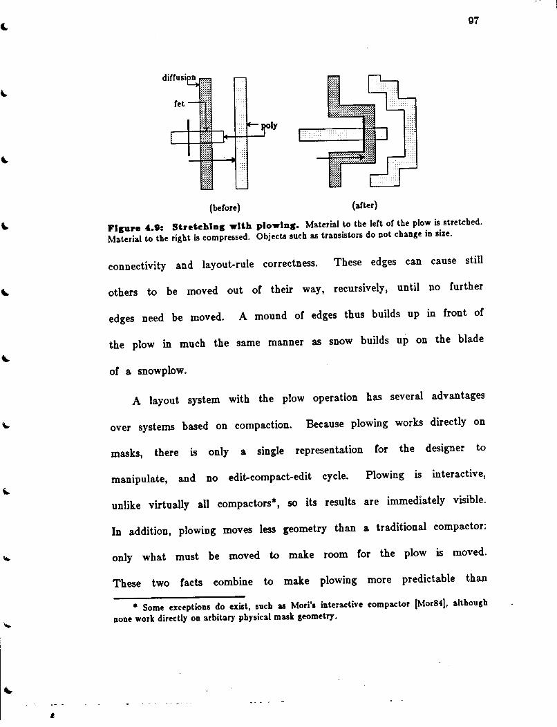
'
Q7
{before) (after)
Figure 4.th Stretching with plowing. Material to the left or the plow is stretched.
Material to the right is compressed. Objects such as transistors do not change in size.
connectivity and layout-rule correctness. These edges can cause still
others to be moved out of their way, recursively, until no further
edges need be moved. A mound of edges thus builds up in front of
the plow in much the same manner as snow builds up on the blade
of a snowplow.
A layout system with the plow operation has several advantages
over systems based on compaction. Because plowing works directly on
masks, there is only a single representation for the designer to
manipulate, and no edit-compact-edit cycle. Plowing is interactive,
unlike virtually all compactors*, so its results are immediately visibleo
In addition, plowing moves less geometry than a traditional compactor:
only what must be moved to make room for the plow is moved.
These two facts combine to make plowing more predictable than
• Some exceptions do exist, such as Mori's interactive compactor (Mor84J, although
none work directly on arbitary physical mask geometry.

98
compaction. Finally, plowing provides direct control over which parts
of a layout to move, thereby giving designers the greatest possible
amount of flexibility.
4.3. Plowing algorithm
Plowing works by finding edges and moving them. An edge is a
boundary or a piece of a boundary, parallel to the plow, between
material of two different types. When an edge moves, the material to
its leftt is stretched, and the material to its right is compressed.
The main loop of the plowing algorithm consists of selecting an
edge to move, determining what new edges must also move if the
selected edge moves, and then later processing these new edges.
Initially, the algorithm will process those edges hit by the plow as it
moves from left to right.
Plowing processes a single edge by applying a collection of rules
that tell it what areas to search for new edges, and how far these
new edges must move. These rules are parameterized by layout rules,
specifying minimum widths and spacings, that come from a technology
file. The next few sections will present the most important of the
plowing rules, progressing from the simplest to the more complex.
t For the sake or simplicity, I will explain plowing as though it were always working
rrom ldt to right, although or course it works in all rour directions. See Section 4.5 ror
details.

gg
I believe that these rules represent the essence of what is required
to manipulate physical masks by an operation such as plowing. In
effect, they extract certain structural information from a layout, and
ensure that plowing preserves its following properties:
• Manufacturability. Plowing must preserve layout-rule correctness by
maintaining minimum widths and spacings, in order that the circuit
is fabricatable. The rules for clearing the shadow and sliver
prevention are necessary for this purpose.
• Electrical connectivity. Plowing must neither introduce new
electrical nodes nor destroy existing ones, and must not change the
nodes to which each transistor is connected. Two kinds of rules
ensure this: one for maintaining connectivity between different
materials, and one for preserving attachments to subcells.
• Electrical function. The sizes of certain components, such as
transistors and contacts, have been chosen carefully by the designer
and should not be altered. Plowing has special rules to prevent it
from changing the shape or size of these structures.
The rules to preserve these properties may overlap, m the sense
that a given edge may be forced to move as a result of several
different plowing rules. However, simplicity rather than a desire to
minimize the overlap between rules has guided their selection.
Alter presenting these rules for processing a single edge, this
section will focus on the order in which edges are considered for
processing. Although depth-first order has the advantage of conceptual
simplicity, it has a worst-case running time that is exponential in the
number of edges in the layout. The plowing algorithm actually uses a
breadth-first order. It processes each edge only when the positions of
all edges to its left are known, resulting m a running time that lS

100
linear in the number of edges in the layout. This points out a
similarity between plowing and critical-path compaction: both are
essentially finding the longest path in a graph. Plowing differs from
critical-path compaction, though, in that it never constructs the graph
explicitly; rather, it uses the plowing rules to find the arcs of this
graph implicitly as plowing progresses.
4.3.1. Clearing the shadow
The first plowing rule is intuitively obvious: when an edge moves,
also move any edges it hits or approaches too closely. Figure 4.10
depicts a trivial layout consisting of three unconnected pieces of
diffusion. The edge labelled e IS to be moved to a final position
indicated by the arrowhead. At the very least, the rectangular area
violation
B Bl ..............
(a) (b) (c)
Figure 4.10z Clearlns \he umbra. When the edge e moves, all edges in area A (the
area swept out by e) must be moved (a). Moving only these edges results in edge f moving
but not edge g. This leaves a layout-rule violation (b) between e and g, because the
minimum spacing between two pieces or diffusion is ' units and these two edges are closer.
Searching area B as well as area A avoids this problem. The width or B is the minimum
separation rule '· The two areas are referred to collectively as the umbre~ or edge e.

'
101
labelled A must be swept clear of any other edges before edge e can
be moved. However, because of the spacing rules between two pieces
of diffusion, any material inside area B would then be too close to
the newly moved edge. Consequently, the area to be swept includes
both areas A and B. The union of these two areas is referred to as
the umbra* of the edge e. If an edge whose bottom is at ybot and
whose top is at ytop is moved from an initial x-coordinate of xbot to
a final position of xtop, it sweeps out the area of the rectangle
( xbot, ybot, xtop, ytop ). The umbra IS the larger rectangle
(xbot,ybot,xtop+d,ytop), where d IS the design-rule distance.
w! penumbra
e
w! (a) (b) (c)
J'lsure 4.111 Clearlas the peaumbra. When the edge e moves (a), edges in its
umbra must be moved to the right. It only edges in the umbra are moved, however, the
result can be electrical disconnection (b). To avoid this, plowing also moves edges in the
penumbra to the right, giving the correct result shown in (c). The height or the penumbra is
the minimum width or the material, w. This has the errect or inserting jogs automatically.
• In a solar eclipse, the umbra is that portion or the moon's shadow rrom which the sun
appears to be completely eclipsed. The penumbra is the partial shadow surrounding the
umbra. In plowing, the umbra or an edge contains edges directly in its path, while the
penumbra contains edges to either side or its path but nonetheless too close.

102
Plowing must also search above and below the umbra to prevent
the edge from sliding too close to other edges above or below it.
Figure 4.11 shows why this 1s necessary. If material were moved out
of the umbra alone, as m Figure 4.11b, the result 1s electrical
disconnection. To avoid this, plowing must also move edges out of
the areas above and below the umbra. The correct result is shown m
Figure 4.llc. The areas above and below the umbra are referred to
collectively as the penumbra. Jog insertion lS an automatic
consequence of searching the penumbra. Moving edges out of the
penumbra also prevents electrical shorts, as can be seen by reversing
the roles of material and space in Figures 4.1la-c.
e e
(a) (b)
e (c) (d)
Flsure 4.12a Penumbra outline. II e's penumbra included all or area A, as shown in
(a), then edge I would be round and moved, resulting in (b). This is undesirable, since I need
not move in order to preserve layout-rule correctness and connectivity. A better derinition or
the penumbra is area B only, as shown in (c). Searching this area results in only the edge g
being round and moved, as is necessary to preserve layout rule correctness.
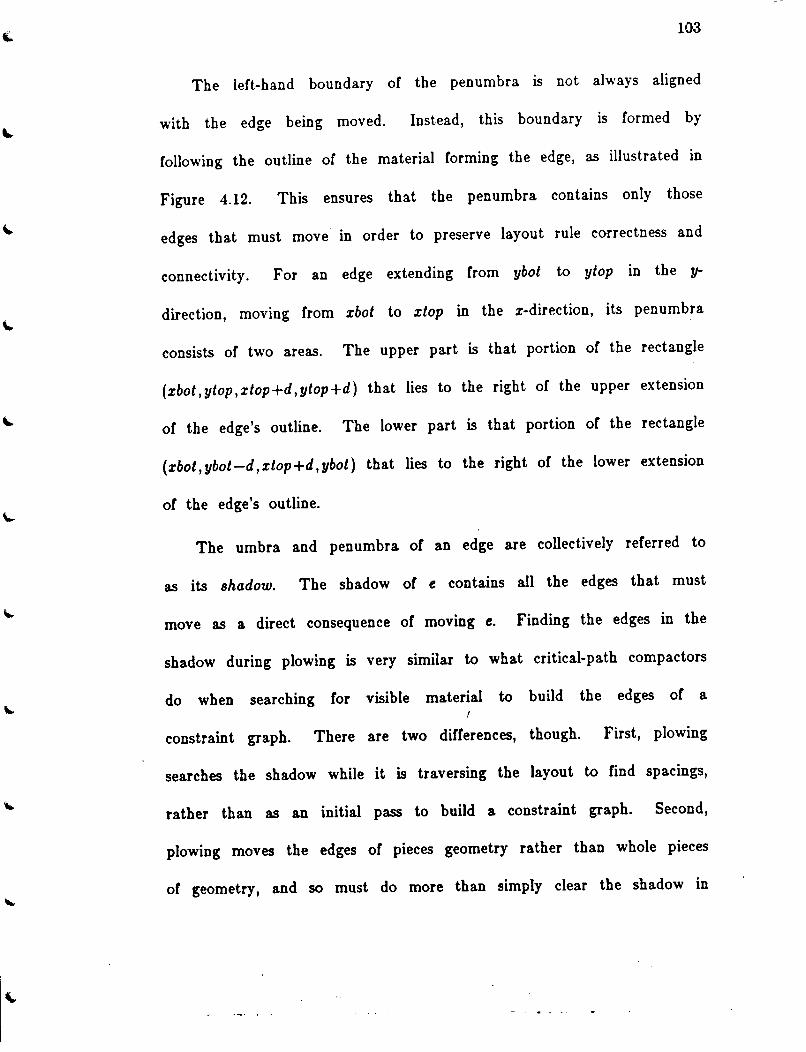
103
The left-hand boundary of the penumbra is not always aligned
with the edge being moved. Instead, this boundary is formed by
following the outline of the material forming the edge, as illustrated in
Figure 4.12. This ensures that the penumbra contains only those
edges that must move in order to preserve layout rule correctness and
connectivity. For an edge extending from ybot to ytop in the y
direction, moving from xbot to xtop in the x-direction, its penumbra
consists of two areas. The upper part is that portion of the rectangle
(xbot,ytop,xtop+d,ytop+d) that lies to the right of the upper extension
of the edge's outline. The lower part is that portion of the rectangle
(xbot,ybot-d,xtop+d,ybot) that lies to the right of the lower extension
of the edge's outline.
The umbra and penumbra of an edge are collectively referred to
as its shadow. The shadow of e contains all the edges that must
move as a direct consequence of moving e. Finding the edges in the
shadow during plowing is very similar to what critical-path compactors
do when searching for visible material to build the edges of a
constraint graph. There are two differences, though. First, plowing
searches the shadow while it is traversing the layout to find spacings,
rather than as an initial pass to build a constraint graph. Second,
plowing moves the edges of pieces geometry rather than whole pieces
of geometry, and so must do more than simply clear the shadow in

104
order to avoid design-rule violations. The following sections describe
the additional rules required by plowing.
The previous examples only involved one type of material. Real
layouts contain may different materials. This complicates clearing the
shadow in two ways. First, there may be several different layout
rules to apply m the shadow. For example, the diffusion-diffusion
spacmg may be 3 units, while the diffusion-polysilicon spacing is only
1 unit. Both rules apply at an edge between diffusion and space, so
two shadow searches are required for such an edge: one extending an
extra 3 units, searching for diffusion, and the other with a 1 unit
extension, searching for polysilicon.
The second complication arises because layout rules apply not to
the nearest edge, but to the nearest edge of a particular type. For
example, in CMOS the spacing rule from p-diffusion to n-diffusion
applies regardless of whether there is any intervening material. As a
result, each shadow search is actually a search for the nearest material
of a specific type, rather than a search for the nearest edge.
4.3.2. Sliver preventioa
The rule described for clearing the shadow guarantees that plowing
never moves one vertical edge too close to another. However, it does
allow violations to be introduced between the new vertical edges that
are formed when material is stretched. These violations take the form

105
violation e
(a) (b) (c)
Figure 4.13: AYoldlng •IIYera. When the edge e moves (a), a sliver of space is
introduced below the horizontal segment h, as shown in (b). To correct this, the left-hand
edge of this sliver, /, is moved along with e, but only as far as the right-hand end of the
segment h (c).
of slivers of material or space whose height is less than the minimum
allowed. Eliminating such slivers requires that their left-hand edges be
moved, as illustrated in Figure 4.13. The left-hand edge of each
sliver lies along the left-hand boundary of the penumbra, so it can be
found when tracing the outline of the penumbra.
Sliver prevention is a necessary consequence of movmg edges,
rather than entire objects, and as such is a problem unique to mask-
level compactors such as plowing. If only entire objects were moved,
new horizontal edges could . never be formed. The flexibility of
plowing that allows it to deform objects by moving their edges is in a
sense paid for by the cost of having to prevent slivers.
4.3.3. Maintaining connectivit7
As well as ensuring layout-rule correctness, plowing must take care
to maintain connectivity between different types of material.
Normally, this connectivity will be ensured automatically by minimum-

106
(a) (b) (c) (d)
l'lcure 4.141 CoaaediTitJ' malatalaed b7 width rule•. Often, connectivity is
maintained by width rules. When the poly-metal contact in (a) is plowed, the width rule
applied in the shadow (b) is for both polysilicon and poly-metal contact taken together. ~a
result, the poly edge is moved along with the contact (c) far enough to leave them connected
by a minimum-width neck or poly (d).
width layout rules. For example, polysilicon and poly-metal-contact
remain connected because there is a width rule for both materials
taken together, as shown in Figure 4.14. However, to ensure that
connectivity is never violated even when no minimum-width rule IS
present, plowing uses the additional rule described in Figure 4.15.
Special care must be also taken to avoid introducing layout-rule
violations as a result of horizontal edges sliding past each other. If
. A,
r----e
(a) (b) (c)
l'lcure 4.1&1 'Malatalalac eoaaedh·tt,.. If edge e is plowed (a), material A may
disconnect from B (b). To prevent this, a segment or edge f is dragged along with e (c). The
height or this segment is the minimum width or material B.

....
............•.... ................. ~~~~~:::tL::: ················· :::.:.:.:::::::::·:·::
(a) (b)
107
A
(c)
Flsure 4.11a Pre•en·lns covered edse.. Allowing certain types or edges to
become uncovered can introduce layout rule violations. For example, all edges or a transistor
must border on either polysilicon or diffusion. In this example, the edge g is moved to
prevent C (rom being uncovered.
one material completely covers a horizontal edge with another material
(for example, the A-C edge in Figure 4.16}, plowing moves the other
material as much as is needed to maintain complete coverage. This
ensures, for example, that transistors are not uncovered by sliding
diffusion completely off their sources or drains.
4.3.4. lnelastie features
Certain features in a layout should not be stretched or compacted.
For example, the sizes of transistors and contacts are chosen for
electrical reasons and should not be altered by plowing. Our
discussion of edge motion has assumed that the material forming both
sides of the edge was stretchable. When material is inelastic, both its
left-hand and right-hand edges must be moved in tandem. This can
introduce ·a cycle of dependencies, which must be resolved if plowing is
not to loop infinitely. Since the way plowing handles these cycles
depends on the order in which it visits edges, further discussion will
be deferred until Section 4.3.7.
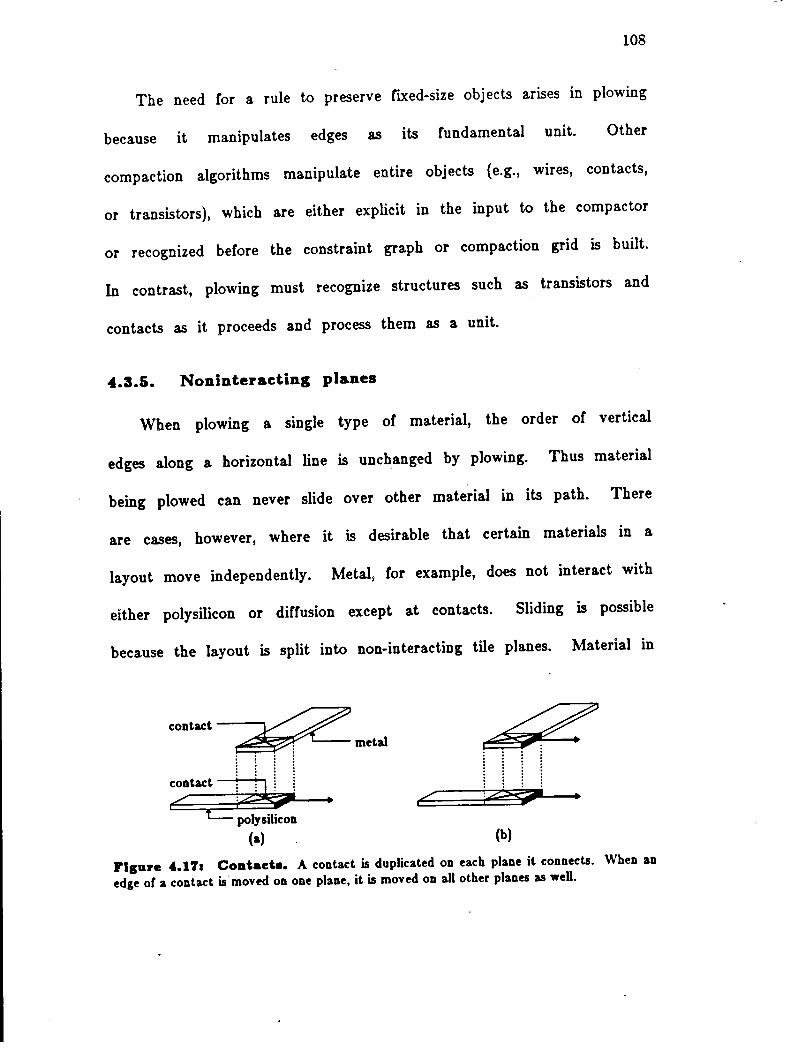
108
The need for a rule to preserve fixed-size objects arises m plowing
because it manipulates edges as its fundamental unit. Other
compaction algorithms manipulate entire objects (e.g., wues, contacts,
or transistors), which are either explicit in the input to the compactor
or recognized before the constraint graph or compaction grid is built.
In contrast, plowing must recognize structures such as transistors and
contacts as it proceeds and process them as a unit.
4.3.&. Noninteraeting planes
When plowing a single type of material, the order of vertical
edges along a horizontal line is unchanged by plowing. Thus material
being plowed can never slide over other material in its path. There
are cases, however, where it is desirable that certain materials in a
layout move independently. Metal, for example, does not interact with
either polysilicon or diffusion except at contacts. Sliding is possible
because the layout is split into non-interacting tile planes. Material in
contact
I I
(b)
Figure 4.1'1a Coataet•. A contact is duplicated on each plane it connects. When an
edge or a contact is· moved on one plane, it is moved on all other planes as well.

I ...
lOQ
one plane is free to slide past material in any other plane. In our
example, any material in the active plane (poly, diffusion, and devices)
is free to slide beneath any material on the metal plane (metal or
pad).
The plowing algorithm operates on each plane independently. The
only interaction between planes occurs at contacts, which are
duplicated in each plane that they connect. When an edge of a
contact is moved in one plane, the corresponding edge of the contact
in all other planes is moved by the same amount, as illustrated in
Figure 4.17. This also moves whatever the contact connects to in the
other planes, thus preserving connectivity.
4.3.1. Subeella and hierareh7
One approach for plowing a hierarchical layout, such as that
shown in Figure 4.18a, is to treat it as though it were non
hierarchical and propagate edge motions inside subcells. This might be
practical if no subcell were used more than once. However, Magic
instantiates subcells by reference, so a change in one instance of a
subcell is reflected in all its other uses. Situations in which a subcell
is used more than once can produce unsatisfiable sets of constraints, as
Figure 4.18b illustrates.
Magic takes a simpler approach, which IS to v1ew subcells as
"black boxes" to which connectivity must be maintained by plowing,

110
'~'
!il! A B A B
(berore) (arter)
(a)
A B A B
(b)
(berore) (connict)
Flsare 4.18& Plowlas Ia the preaeace of hlerarch;r. (a) Plowing might treat
hierarchy as though it were invisible to the user. Each or cells A and B would be modified.
(b) Cell C is used twice, once nipped lett-to-right and once in its normal orientation. Both
uses rerer to the same master detinition or C. Moving edge e to the right is impossible,
because it requires e to move to the lett in order to keep out or its own path. The more edge
e is moved to the right in the lert-hand use, the worse the violation becomes.
but whose internal structure should not be modified. A consequence
of Magic's approach is that plowing can be used to modify the
placement of cells at the floor plan of a chip, smce it only changes
the location of subcells, not their contents.
When any mask geometry that abuts or overlaps a cell is moved,
the entire cell must move by the same amount. Conversely, whenever

111
a subcell moves, all mask geometry and other subcells that abut or
overlap it must also move by the same amount. The net effect IS
that a cell behaves like flypaper, causing all geometry over its area to
"stick" to it and move as a whole when any part of it is required to
move. This behavior IS similar to that achieved by hierarchical
compactors, although in an extremely simple way: each cell constrains
both its internal geometry and any geometry that overlaps it to be
completely rigid, instead of allowing a limited amount or slack as done
In VTI's hierarchical compactor [Kin84].
In addition to preserving connectivity with subcells, plowing must
also be careful when it moves other geometry to avoid introducing any
layout rule violations with the geometry inside a subcell. One
approach for dealing with this is to define a protection frame (CHK83)
Cor each cell, an outline around the cell into which no material may
be plowed. Magic uses an extremely simple Corm or protection frame:
it assumes that the cell contains all types of material right up to the
border or its bounding box.
For example, in the MOSIS 4p nMOS rule set, the worst-case
layout rule involving diffusion is the diffusion-diffusion spacing rule of
6 microns. An edge with diffusion to its left can be plowed to
within 6 microns or a subcell before that subcell will itself have to
move. The worst-case rule distance involving polysilicon is 8 m1crons,

112
so polysilicon can only be plowed to within 8 microns of a subcell
before the cell must move. Since the contents of subcells are
considered unknown, the closest one subcell can be plowed to another
before the other will have to move is the worst-case layout rule m
the entire ruleset, which in this ruleset lS 8 microns. or course, if
the user wishes to move material closer to a subcell than this, he or
she can still do so using other editing operations beside plowing.
4.3.7. Edge processing order
The above rules describe how to process a single edge. In
addition, however, plowing needs to know the order m which to
process them. A conceptually simple order is that of a depth-first
search. To move an edge, plowing could apply its rules to find all
new edges, recursively move them, and then move the original edge
I (a) (b) (c)
Figure 4.Uh Recur•IYe plowing algorithm. It is conceptually simplest to think
or plowing as a recursive algorithm. To move the edge in (a), first recursively clear space ror
this edge (b), and then move the original edge into the cleared space (c).
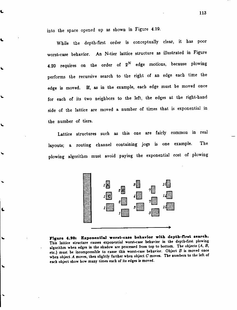
....
113
into the space opened up as shown in Figure 4.19.
While the depth-first order is conceptually clear, it has poor
worst-case behavior. An N-tier lattice structure as illustrated in Figure
4.20 requires on the order of 2N edge motions, because plowing
performs the recurstve search to the right of an edge each time the
edge is moved. If, as in the example, each edge must be moved once
for each of its two neighbors to the left, the edges at the right-hand
side of the lattice are moved a number of times that is exponential in
the number of tiers.
Lattice structures such as this one are fairly common in real
layouts; a routing channel containing jogs ts one example. The
plowing algorithm must avoid paymg the exponential cost of plowing
1 I I 11
I s 71 .
e 1. 1 I .. I .
el 71 .
1 s 1
1 9
l'lsure 4.20: Exponential wor.t-caae behavior with depth-firat aearch.
This lattice structure causes exponential wors~case behavior in the depth-first plowing
algorithm when edges in the shadow are processed from top to bottom. The objects (A, B,
etc.) must be incompressible to cause this worst-case behavior. Object B is moved once
when object A moves, then slightly farther when object C moves. The numbers to the left or
each object show how many times each or its edges is moved.
114
such a structure. It does so by using a breadth-first search that
waits until the final position of an edge is known before it performs
the search to the right of that edge. This strategy causes the
number of edge motions to be linear in the number of edges in the
lattice.
To implement the breadth-first search, plowing maintains a list of
edges to be moved, sorted in order of increasing x-coordinate. On
each iteration, the leftmost edge is removed from the list and the
shadow to its right is searched. Any edges discovered by this search
are placed in the list along with the amount they must move. Since
the final position of an edge can only be affected by edges to its left,
the final position of the leftmost edge in the list is always known.
The original depth-first algorithm allowed the layout to be
modified as plowing progressed, since processing an edge consisted of
first recursively clearing enough space for it, and then moving the
edge into the cleared space. With breadth-first search, this IS
impossible, since edges to the right will not be moved as long as
there are queued edges to the left of them waiting to be moved.
Hence, processing an edge no longer guarantees that there will be
space to its right into which it can safely move.
Instead of. actually updating the layout as it progresses, the
breadth-first version of plowing stores with each vertical edge segment

115
the distance it moves. When all edges have been processed, and the
distance each edge moves has been determined, plowing invokes a
post-pass to update the layout from the information stored with each
edge.
However, if the layout is not modified until all edges have been
processed, special care must be taken to avoid the generation of
slivers. Figure 4.21 illustrates the problem. To process each edge
correctly, it is important to know what other edges have been already
been processed and what their final positions will be. In general, the
plowing algorithm must consider edges whose final positions will be m
the shadow of an edge, rather than those whose initial positions are in
its shadow. These final positions are stored in tiles along with the
initial edge positions, so may be used in place of the initial positions
tual) r- violation
e
(a) (b) (c)
Flsure 4.111 SliTer aToldaace when n•lns breadth-ftrd ••arch. When
processing an edge in the breadth-first approach, it is important to use information about the
final positions or edges that have already been processed. In (a), it has already been decided
to move edge /, but the edge will not actually be moved until all other edges have been
processed. Ir edge e is processed without considering the new position or/, a sliver will result
as shown in (b). Instead, the plowing algorithm must consider the eventual positions or edges
that have already been processed, to produce the result or (c).

116
by the search procedures described in the next section.
Because of the rule in Section 4.3.4, if the right-hand edge of a
piece of inelastic material moves, its left-hand edge must also move.
Figure 4.22 illustrates how this can lead to a cycle of dependencies.
The plowing algorithm avoids infinite loops by comparing the amount
an edge is supposed to move with the motion distance already stored
with the edge. If the stored motion distance is greater or equal, the
edge need not be moved a second time.
In cases where a layout rule violation exists in the original layout,
an infinite loop is still possible. In Figure 4.22, for example, the
distance r between edges I and e is less than s, the minimum
separation allowed. Edge e initially moves by distance d. Plowing
should move all edges found m the shadow of I far enough away so
r
d d r e r e
Flsure 4.111 IDelutle featurea. When inelastic objects are present, plowing may
have to cope with circular dependencies. Tiles A, B, and C all belong to the same material.
When edge e moves by distanced in (a), tile B must move by the same distance to prevent A
from being uncovered. To prevent C from being uncovered, C's left-hand edge must move,
finally causing edge I to move by distance d. Edge e is in fs shadow as a result, but should
not be moved a second time.

117
as not to cause any rule violations with the newly moved f. Hence
edge e would have to move by d+s-r, which is more than the motion
distance stored with the edge. This leads to an infinite loop in which
edge e is moved by an additional s-r.
Plowing avoids this sort of infinite loop by never movmg a
shadowed edge (e) more than the edge causing the shadow (/). This
technique prevents infinite looping in over-constrained situations, but
preserves existing layout rule violations. While it is easy to detect
such situations during plowing and warn the user, the current
implementation of plowing does not do so.
4.4. Searching algorithms
Virtually all of the plowing rules described in the previous sections
make use of two powerful searching procedures: shadow search and
outline search. The use of corner-stitching makes these procedures
both simple and fast.
4.4.1. Shadow search
The first searching procedure, shadow search, 15 used when
clearing the umbra and penumbra, and also when applying the rules
to maintain connectivity. It searches to the right of an edge for
edges that are "visible" from the original edge, treating a specified set
of tile types as "invisible". Effectively, it finds the shadow of the

(a)
ndirr
(b)
~- - - - - - ~ '" - (poly. pdi!f}
1
e 1
1 I 1 ld - {pdiff}
--------...J
118
Figure 4.23: Shadow •earch. A shadow search starts with an edge e and a set or tile
types 1et. It returns all edges to the right of e that are "visible" from e, where 1et is the
collection or visible types. The edges found have some type in 1et on their RHS, and only
types not in 1et on their LHS back to e. In (a), 1et contains poly and pdiff; edges round by
the shadow search are shown in bold. In (b), 1et contains only pdiff; the effect is as though
the central poly tile were invisible.
original edge, cast to its right onto types not in the invisible set, as
illustrated in Figure 4.23. The search to the right is limited so that
only edges within a particular distance of the original edge are
considered.
The notion of visibility is necessary because width and spacmg
rules involve only certain kinds of materials, and ignore others. In
the MOSIS 3p CMOS process, for example, there is a rule requiring
p-diffusion and n-diffusion to be separated by 16p. This rule applies
regardless of the type of material between the two types of diffusion.
In Figure 4.23, it would not be apparent that the p-diffusion would
have to move as a result of the n-diffusion moving, unless shadow
search allowed plowing to "see through" the intervening polysilicon.

.,.
119
pdirr poly ndirr
.... f~·:···_···· _···~-·····+··_···· _···~---::~-- ·--~ K<·:·:·:<·:·:--[1""······+ ·~~·i+······-t :.:,::::::
(a) i+ ······· ~~~-· (b)
···+~~;:m.······························ + ~::' :::: t+"""
~~::::::;:;:;::::~ •....... t. ······ ·! ~ ~ • +
.. ..... :-:~;:;:;:=r~·························
(c) ~==~==========~t1----·r-.:.¥:«~·--··:~"" :n -. . .... (d)
•······· . (e)
~--························ ~::;:3tili~ •....... ~. ~~!-········-······-·····
t ~:::::::::•
(g) •...... f-l«='»:'l~·······: +::::~:.: ... - _., ~ ~ :_;,;-
......... ~--························
Flpre 4.i4a Shadow •eareh example. Starting with the RHS or the pdirr tile in
(a), and given a "visible" set consisting or ndiff, (b) through (f) show the edges and tiles
visited by the shadow search algorithm, in the order they are visited. Each tile is visited
once from each or its left-hand neighbors that lie between the bottom and top or the original
edge. This means that some tiles may be visited more than once, such as the ndifC tile on
the right.
Using corner-stitching, shadow search is implemented as a recursive
procedure. The recursive portion is to find those tiles in the shadow
or the right-hand side or an initial tile t, between the y-coordinates
ybot and ytop. The example in Figure 4.24 illustrates the following
algorithm:

120
SHADOW!. Visit each tile r along the RHS of t, by first following
the TR switch of t and then following the LB stitches
of each r. Do this until the top of r is < = ybot.
Ignore each tile r found above whose bottom is > = ytop.
SHADOW2. For each type r above that is not ignored, if the type of
r is not in set, report the edge formed by the LHS of r,
between J.fiN(ytop, TOP(r}) at the top and
MAX(ybot,BOTTOM(r)) at the bottom.
SHADOW3. Otherwise, the type of r is in set, so we want to see
through it to tiles to its right. Recurse, with a new ybot
and ytop of MIN(ytop, TOP(r)} and MAX(ybot,B01TOA1(r))
respectively.
In practice, it is only necessary to search a shadow for a limited
distance to the right of an edge, e.g., the distance the edge moves
plus the distance of the layout-rule being checked. To accomplish
this, step SHADOW2 checks to see if the edge is already farther to
the right than the right-hand side of the shadow, and if so, does not
report it. To avoid "seeing" edges that have already been processed
by the plowing algorithm, shadow searching uses final edge positions
instead of initial ones. Figure 4.25 gives the complete shadow search
algorithm.
· 4.4.2. Outline aeareh
The second search procedure, outline search, is used to trace the
boundary of the penumbra and also in sliver avoidance. The outline
search is given a set . of tile types and a starting point on the
boundary between a tile in the set and a tile not in the set. From
the starting point, it will visit a series of. horizontal and vertical

L
..
ShadowSea.rch(pla.ne, area, YisTypes) PlaDe "plane;
{
}
a-t •area; TUeT)-peS.t YisTypes;
Polat startPoint; lat bottom; a-t edge; TUe *t;
edge.r_ytop- area->r_ytop;
/* Walk along the LHS of the 1weep area frtnn top to botttnn 'r startPoint.p_x- area->r_xbot; startPoint.p y- area->r ytop- 1; wbUe (startPoint.p_y >--area->r_ybot) {
}
/*find the nut tile along the LHS of the 1earch area 'r t- FindTileContainingPoint(plane, &startPoint); startPoint.p _y - BOTTOM( t) - 1;
bottom- MAX(BOTTOM(t), area->r_ybot); lf(FINALRIGHT(t) >- area->r_xtop) edr;e.r_ytop- bottom; elae ShadowRHS(t, area, okTypes, &edr;e, bottom);
ShadowRHS(t, area, •isTypes, bottomLert, edr;e) Tile *t· lleet •~ea;
{
TUeT7peSd ,-isTypes; lat bottomLeft; a-t *edge;
lat bottom, left; Tile *r;
;• Walk along the RH S of • t • frtnn top to botttnn 'r r - TR(t), left - LEFT(r); ... { ;•
• OnlJI proce11 tile~ between edge->r _JJtop (on the top} • and bottO'rr&Uft (on the botttnn}. ,
bottom- MAX{bottomLeft, BOTTOM(r)); lf(bottom < edr;e->r_ytop) {
}
If (SetCont.ains(•isTypes, TileType(r))) {
}
edr;e- > r _x - left; edr;e->r_newx- LEFT(r); edr;e->r_ybot- bottom; •.. process the edge; edge->r_ytop- edge->r_ybot;
elae If (FINALRIGHT(r) >- area->r_xtop) edge->r ytop- bottom;
elae ShadowRHS{r, area, YisTypes, bottom, edge);
121
ShadowSearch
ShadowRHS

122
r- LB(r); } wlaUe (TOP(r) > bottomLett);
}
Flsure 4.2&& Shadow-•earch alsorUhm. The input is a corner-stitched tile plane, an area, and a set or visible types.
. .. . ... :::::::::::::::::x
··············
.. ........
-P
(a)
i dir
-P dir i
(b)
Flcure 4.21& Outllae ••arch. Given a set or tile types ut, a starting point P, and a direction dir, outline search will visit all the edges along the boundary between material in 1d and material not in 1d. (These edges are shown with bold lines). In (a), 1d contains poly only. In (b), 1et contains poly and poly-metal-contact. In both examples, the caller chose to abort the search after visiting the edge labelled X.
edges, always keeping material in the set to its left. As each edge is
processed~ the caller has the choice of either continuing the search or
stopping it. Figure 4.26 illustrates two examples. Most callers choose
a stopping point based on the coordinates or the endpoint or each
edge found by outline search in relation to the edge being processed.
Since the choice or stopping point is the caller's responsibility, rules
such as sliver elimination are free to use the final edge positions
instead of initial positions, as described in Section 4.3.7.
The algorithm to implement outline search has two parts,
illustrated _in Figure 4.27. The input to the algorithm is a starting
point P, a set of types set, and an initial direction dir. This initial

• qleft : qright
-- ~---qbl : "-- starting point
(a)
turning right .-----•• new dir: right
starting
(c:)
turning left new dir: lert ... ---.,
(b)
starting point
(d)
123
l'lsure 4.271 Outline aeareh alsorlthm. The first step or outline search (a) is to
determine whether to turn left or right. The algorithm does this by looking at the material
in quadrants labelled qleft and qright. Jr it turns left (b) or right (c), it follows the stitches
shown to obtain a new tile in qlejt and qright and then begins to go in the new direction. Ir
it keeps going straight (d), it moves to the next point where material in qlejt or qright
changes. In this example, where it is moving up, it follows the TR stitch and then walks
down along the RHS to the new starting point. If material had not changed along the RHS
at all, the algorithm would have followed the RT stitch to the tile above qlejt and repeated
the step in (a).
direction should be chosen so that when facing in direction dir, there
is material or a type in set in the quadrant that is behind us and to
our left, i.e, quadrant qbl 1n Figure 4.27. The outline search
algorithm is as follows:
OUTLINE!. Find the type or material in the quadrants labelled qleft
and qright in Figure 4.27a. This is done initially by
using the corner-stitching point-search algorithm to find
the tile or tiles in each or the two quadrants; on
subsequent iterations, these tiles will be found as indicated
---.

124
m steps OUTLINE2 and OUTLINE3.
OUTLINE2. If the material in qleft does not belong to set, turn left
(rotate dir by QO degrees to the left) and go to step
OUTLINE!. Use the tile originally in qleft as the tile in
the new qright, and follow the stitches shown in Figure
4.27b to find the tile in the new qright.
OUTLINE3. If the material in qright belongs to set, turn right and go
to step OUTLINE!. Use the old tile in qright as the tile
in the new qleft, and follow the stitches shown in Figure
4.27c to find the new qright.
OUTLINE4. We know that qleft contains material in set, and qright
contains material not in set. Move forward in direction
dir to the next point at which the material in qleft or
qright changes. See Figure 4.27d.
The details of the steps above will vary depending on the direction
dir currently being followed. For example, when moving up it is best
to follow the RT stitch of the left-hand tile, and then follow the
LB stitches of the tiles along its right-hand side to find the closest
point of interest. When moving left it is best to follow the BL
stitch of the right-hand material (which will really be on the top), and
then the TR stitches along its bottom.
The total number of tiles visited in the course of tracing an
outline depends on the local geometry. However, it lS possible to
determine the average number of tiles visited by using the average
number of neighbors of a given tile. Ousterhout's paper [Ous84a)
computes the average number of neighbors as 6, or between 1 and 2
per side. Using the higher figure of 2 neighbors per side, we can
expect OUTLINE2 and OUTLINE3 each to follow an average of two
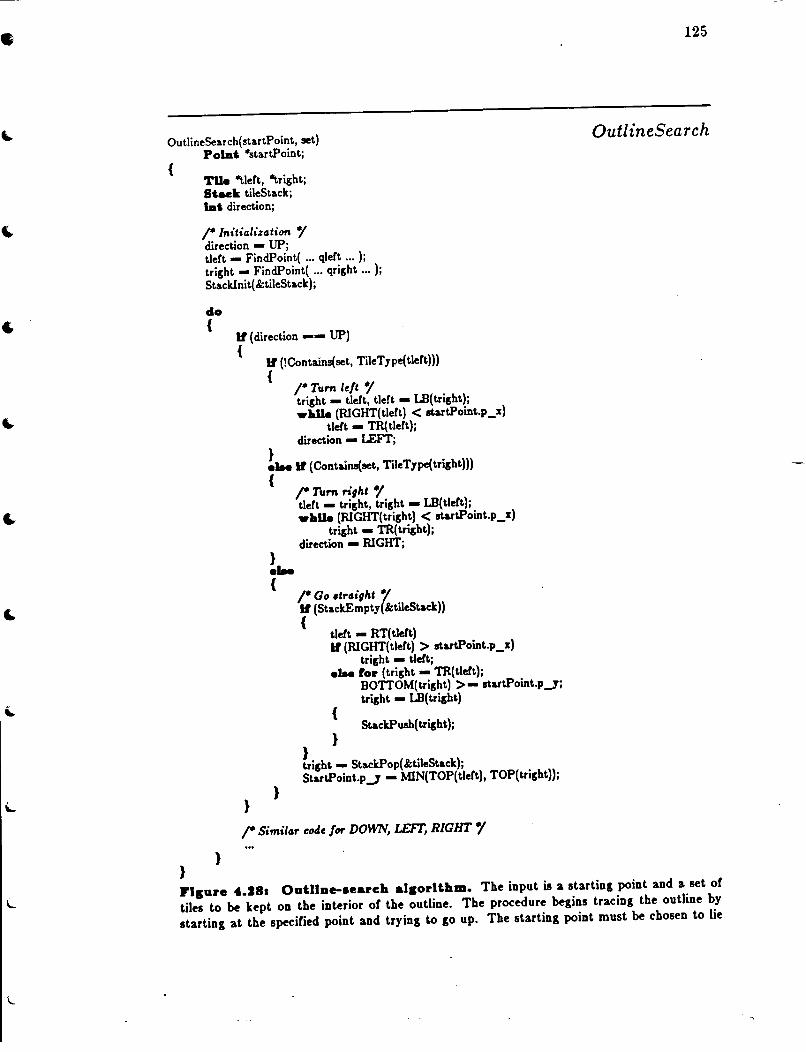
•
OutlineSearch(startPoint, set) Pobat •startPoint;
{
}
TUe ~left, ~right; Steck tileStack; bat direction;
j• Initialization f direction - UP; tleft - FindPoint( ... qleft ... ); tright - FindPoint( ... qright •.. ); Stacklnit( &tileS tack);
clo {
}
If (direction -- UP) {
}
If (!Contains(set, TileType{tleft))) {
;•rum left r tright - tleft, tleft - LB(tright); wlaUe (RIGHT(tleft) < st.artPoint.p_x)
tleft- TR{tleft); direction - LEFT;
} .... If (Contains(set, TileType{tright))) {
} .... {
}
j• Tum right f tleft - tright, tright - LB(tleft); wlaU. (RIGHT(tright) < st.artPoint.p_x)
tright- TR(trilht); direction- RIGHT;
j• Go ttroight f II (StackEmpty( &tileStack)) {
tleft - RT(tleft) II (RIGHT(tleft) > st.artPoint.p_x)
tright - tleft; .... for (tright - TR{tleft);
BOTTOM(trilht) >- st.artPoint.p_1; tright - LB(tright)
{ StackPush{ trilht);
} } tright- StackPop{&tileStack); StartPoint.pJ- MIN(TOP(tleft), TOP(tright));
j• Similor code for DOWN, LEFT, RIGHT f
125
OutlineSearch
Flsure 4.28a Oatllae-•eareh alsorlthm.. The input is a starting point and a set or
tiles to be kept on the interior or the outline. The procedure begins tracing the outline by
starting at the specified point and trying to go up. The starting point must be chosen to lie

126
along the right-hand side of some tile whose type belongs to the set.
horizontal stitches for each turn. St~p OUTLINE4 visits an average of
two tiles on its right for each tile on its left. Hence, the total
number of tiles visited should be about twice the number of tiles
along the inside of the outline.
Both search procedures can only find edges or trace outlines that
are represented explicitly 10 corner-stitched planes. For example,
shadow search can't be used to find an "edge" between polysilicon
and metal, smce they are never stored on the same plane.
Fortunately, the rules used to assign tiles to planes ensure that if two
tiles live in different planes, there are no layout rules that involve an
edge between those two tiles, and so plowing need never consider such
edges.
4.&. Extensions
Section 4.3 described the core of the plowing algorithm. This
section extends the algorithm in several ways to make it more usable.
It describes how to plow in four directions, how to limit the area
affected by plowing, how to avoid compressing wire widths, and how
to control the number of jogs introduced.

~ 127
....
4.6.1. Plowing in tour directions
Plowing must work in all four directions if it IS to be useful.
There are several ways m which this can be done. One way ts to
have four copies of the plowing code, one for each direction. This
seems needlessly wasteful, though, smce everything except the stitches
and the sense of some comparisons would be the same m each of the
four copies of the code. In addition, such an approach makes the
code four times as time-consuming to modify.
An alternate approach is to parameterize a single copy or the
plowing code to work in four directions. In fact, I tried this
approach in the original version of plowing by using macros to
generate four different versions of each procedure at compile time.
However, this approach was prone to programming errors, since it was
difficult to remember where to insert parameterization. Also, it was
time-consuming to debug, since the code must work in all four
directions. I eventually abandoned the macro approach in favor of the
one described below.
The solution now used in plowing is to copy the layout into a
temporary cell before plowing. The copy operation rotates the layout
so that the plowing direction is left-to-right in the temporary cell (see
Figure 4.2Q). Plowing is performed on the temporary cell, and the
results are then rotated in the opposite direction and copied back into

'
: ~~t;~~~~;f;~~~ ~f;J;?;~~~~-: I I
I I
I I
(a) (b)
I I
I I
I I
I I
I
I I I I
128
(c) (d)
Flsure 4.10: Tranaformlns the layout before plowlns. Instead or having
plowing code that works in Cour directions, it is easier to have a version that works from
leCt-t~right, and transform the input layout each time before plowing. For example, to plow
from top-t~bottom (a), make a copy or the original layout that has been rotated 90 degrees
counter-clockwise (b), plow it (c), and copy back to the original layout by rotating 90 degrees
clockwise (d).
the original cell. In other words, instead of transforming the plowing
algorithm, transform its input and output.
This approach seemingly requires the entire cell to be transformed
and copied, even if only a small portion is being modified by plowing.
Fortunately, this overhead can be avoided by transforming and copying
the layout as it is plowed, copying only the area that participates in
the plow operation. For each edge being processed, the area that can
be immediately affected by plowing is easily determined from the
plowing rules, as shown in Figure 4.30.
Figure 4.31 illustrates how this strategy is applied. Given that
the original layout already has to be updated by plowing, and also
that a substantial fraction of the time spent in plowing is spent
searching, the cost of the additional copy required by this approach is
small, generally under 20 percent.

-
'
(a)
(b)
d -§
:---------------------------] !d (worst-case design-rule distance) :
1:1 ·+ d initial position final position
d r··----------------------------------; ld
•. <I•L ....... , !d
·--------------·-·······---·····-····-· ld -d
129
Flaure 4.30: Area affected b7 moYina each edae. Each time plowing processes
an edge, it searches for new edges to move in an area that will normally be within the halo
shown in (a). This is true because the rules for clearing the shadow, and sliver avoidance
both search at most the worst-case design rule distance to the right, top, and bottom of the
path from the initial position or the edge to its rinal position. The connectivity rule searches
along the top and bottom or this path, and the contact rule along its lert-hand side. Only
when moving a raxed-width object is it possible that more area must be processed; in this
case, it is a halo around the raxed-width tile or cell (b).

Original layout
Plowing Hll area 1 _,
Original layout
Plowing area
(a)
t::;:;:;:;:;:;:~?.::::;:;:;:~;:::;:;:;:;:;:::::l
~:=l=::::::::::4::::::::::::::::::::=::t~
(e)
area copied _r s ___ _
area copied
(b)
~:;:;:;:;:;:;:;:;:;:;:;:;:;:;:;:;:;:;:;:;:;::::~1
j::::::::;:;:;:::::::;:;:;:;:;:::::::::;:;:;:::~
(r)
h::::::::;::;:;:;:;:;:;:;:;:;:;:;:;:;:~::::d
llli~::;:;:;:;.;:;:;:;:;:;:;:;:;:;:;:;:;~
- -· (c)
(g)
L====================================~====d J::;:;:;:;:;:;~:;:;:;:;:;:;:;:;:;:;:;:;:;:;::::t
- -· (d)
update
130
J'lgure 4.31s Incremeatal traa•form aad cop7. Initially, only a small area
around the plow (a) is transformed and copied to the plowing area, where plowing actually
takes place (b). Whenever plowing is ready to move an edge, it checks to see if that edge is
close enough to the boundary or the copied area ror any layout rules to apply. Ir so, as in
(c), additional area is yanked before searching for additional edges, until either no more edges
are found or the entire initial cell has been transformed and copied (e). Arter the layout in
the plowing area is updated (r), it is transformed back to the original layout, which it
replaces (g). The area yanked each time is chosen to be some multiple or the area already
copied, e.g, four times the area. This ensures that the number or copy operations grows
logarithmically, and that the total area copied grows linearly with the area affected by
plowing, so the overhead or copying remains small.

'
131
4.6.2. Limited plowing
Plowing will ordinarily propagate the effects of moving an edge as
far as necessary to ensure that all the plowing rules are satisfied.
Sometimes, however, it is desirable to prevent the effects of a plow
operation from propagating too far. For example, one may wish to
make changes to the interior of a cell without changing the size of its
bounding box. Alternately, one may wish to avoid changing the
locations of certain wires in a cell as a result of plowing.
The effects of plowing may be limited by placing a boundary in
the layout. A boundary is a rectangle around the plow that prevents
any geometry outside it from being modified as a result of a plow
operation. When a boundary is present, plowing may require two
passes to compute the position of each edge instead of one. In the
r __ ~boundary
I
:e~ I
I-+ L-----...1 fl
(a)
eM+ I
I ....-+ L., _____ Jd
(b)
1------I
d I ~
I !___.._ I
•--e~-·
(e)
Flsure 4.11• Boaodarlee to limit the etred of plowlos. In the three eases
where an edge e extends outside the boundary, the amount by which the plow moved too rar
is the distance d. Jr the plow were to move less by this distance, the edge e would not move
outside or the boundary. In (a), e lies to the right or the boundary. In (b), e lies inside the
boundary but its final position is outside. In (e), e extends below the bottom or the
boundary.

132
first pass, as each edge is processed, plowing checks to see whether
that edge has either crossed the boundary or is already beyond it. If
so, plowing remembers the maximum distance beyond the boundary
that any edge· moved. After this first pass, if any edge moved
beyond the boundary, plowing reduces ~he plow distance by the
maximum distance beyond the boundary recorded in the first pass. It
then re-plows; this second pass is guaranteed to modify no geometry
outside the boundary.
Extending the plowing algorithm to handle a boundary requrres
making the following tests every time the algorithm wishes to move an
edge e:
BOUNDl. Initialize max to zero.
BOUND2. If any portion of e's extends outside the boundary, update
max if the distance e moves is greater than the original
value of max. Then discard the edge e. It may be
discarded because it can't cause any edge outside of the
boundary to move by any more than e moved itself; see
the discussion of circular dependencies at the end of Section
4.3.7.
BOUND3. If e's original position is entirely inside the boundary, but
its final position is to the right of the boundary, update
max to the distance e moves to the right of the boundary,
if this latter distance is greater than max. Do not discard
e in this case, but apply the plowing rules normally.
If e's initial and final positions both lie entirely inside the boundary,
proceed normally. Figure 4.32 gives examples of the above tests.
If one of the above tests succeeded, at the end of plowing the
value max is the distance by which the plow moved "too far." In
. ... . . . . - .·~-
133
this case, plowing does not update the layout. Instead, the original
plow distance is reduced by max, to guarantee that the boundary
constraints will be not violated, and the plowing algorithm IS re-run.
At the end of this second plow, the layout can be updated
successfully.
The notion of boundary is easily extended. For example, it would
be possible to place a different kind of boundary that prevented
plowing from modifying anything on its inside. A similar set of tests
would need to be applied when movmg each edge to ensure that no
edge crossed from the outside of one of these boundaries to its inside,
and that no edge on the inside of a boundary moved.
4.6.3. Wire widths
The layout rules applied by the plowing algorithm correspond to
minimum widths and spacings. H a wire is already minimum-width,
these rules ensure that it is not compressed. If a wire is initially
larger than minimum-width, however, it is possible for plowing to
compress it back down to minimum size. Since wires larger than
minimum-width usually are made wide for a reason-for example,
power and ground may be wider to carry additional current-this
behavior on the part of plowing is unacceptable.
In practice, plowing avoids compressing wires past their true
minimum width. Whenever the left-hand edge of some material is

134
before
·~·~ I (a) (b)
Figure 4.33: Adual width of material. Plowing never compresses material to less
than its real width w. When plowing across the width or an object, as in (a), it is essentially
incompressible. When plowing across its length, as in (b), it may be compressed down to the
computed width w.
being moved, plowing computes the real width of that material, as
shown in Figure 4.33. The minimum distance associated with the
layout rule is replaced by the true width computed by plowing, thus
ensurmg that the material is not compressed in the direction of its
width.
The width of material belonging to an edge e is computed usmg
an algorithm that finds the rectangle with the largest minimum
dimension and the following two properties:
• It is completely contained in the material to the right of e.
• Its left-hand side completely contains e.
The width of material is then taken to be the length of whichever
side of this rectangle is smallest. Figure 4.34 gives several examples.

135
~ I
. ........ ...__ .
l
I J
I
Figure 4.34: Deftolns a material'• width. The width-rinding algorithm rinds the
rectangle with the largest minimum dimension that is completely contained in the material r,
and that completely contains the edge e.

136
Sl S2
(a) {b) (c)
Sl
(d)
Flsure 4.35& FlndlOJS the larged contained redansle. Starting with the
initial estimate for the largest contained rectangle (a), we clip away space tiles. After seeing
tile Sl in (b), there are two choices for clipping: either clip the right-band part or the
rectangle away, or clip the top away. Clipping the top away results in a rectangle with
larger minimum side, 50 we choose it initially. In (c), there is only one choice, namely clip
away 52 from the right or the rectangle. In (d), we consider the other choice, clipping away
Sl from the right or the rectangle, but the resulting width, we, is less than w obtained in (c)
50 we do not consider the path resulting from this clipping any further. Having considered
all possibilities, we are left with a material width or w.
The algorithm has two parts. The first obtains a simple upper
bound on the width of material, using this to construct an initial
rectangle. The second part successively chips away at this rectangle
by removing portions or it that lie outside or the material of interest,
until it satisfies both or the above two properties. Figure 4.35
illustrates the following algorithm:
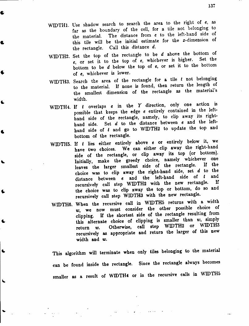
•
I~
WIDTH!.
'WIDTH2.
WIDTH3.
WIDTH4.
137
Use shadow search to search the area to the right of e, as
far as the boundary of the cell, for a tile not belonging to
the material. The distance from e to the left-hand side of
this tile will be the initial estimate for the x-dimension of
the rectangle. Call this distance d.
Set the top of the rectangle to be d above the bottom of
e, or set it to the top of e, whichever is higher. Set the
bottom to be d below the top of e, or set it to the bottom
of e, whichever is lower.
Search the area of the rectangle for a tile t not belonging
to the material. If none is found, then return the length of
the smallest dimension of the rectangle as the material's
width.
If t overlaps e in the Y direction, only one action is
possible that keeps the edge e entirely contained in the left
hand side of the rectangle, namely, to clip away its right
hand side. Set d to the distance between e and the left
hand side of t and go to WIDTH2 to update the top and
bottom of the rectangle.
WIDTHS. If t lies either entirely above e or entirely below it, we
have two choices. We can either clip away the right-hand
side of the rectangle, or clip away its top (or bottom).
Initially, make the greedy choice, namely whichever one
leaves the larger smallest side of the rectangle. If the
choice was to clip away the right-hand side, set d to the
distance between e and the left-hand side of t and
recursively call step WIDTH2 with the new rectangle. If
the choice was to clip away the top or bottom, do so and
recursively call step WIDTH3 with the new rectangle.
WIDTH6. When the recursive call in WIDTHS returns with a width
w, we now must consider the other possible choice of
clipping. If the shortest side of the rectangle resulting from
this alternate choice of clipping is smaller than w, simply
return w. Otherwise, call step WIDTH2 or WIDTH3
recursively as appropriate and return the larger of this new
width and w.
This algorithm will terminate when only tiles belonging to the material
can be found inside the rectangle. Since the rectangle always becomes
smaller as a result of WIDTH4 or in the recursive calls in WIDTHS

'
Width(edge, widthTypes)
{
}
Red •edge; TUeT7peSet widthTypes;
Ked estimate; latd;
;• Shodow eeorch to the right of edge for G twe not in widthTwe• r d - ... initial estimate or width .•. ;
/*Compute initiol eetimote 'Y estimate.r_ytop- MAX(edge->r_ybot + d, edge->r_ytop);
estimate.r_ybot- MIN(edge->r_ytop- d, edge->r_ybot);
estimate.r xbot- edge->r xbot; estimate.r:xtop- edge->r:xbot + d;
/* Recureive port 'Y ret1ll'a WidthClip(edge, widthTypes, &estimate);
WidthClip(edge, widthTypes, estimate) a-t *edge;
{
TlleT7peSd widthTypes; Jlaet *estimate;
lat xw, yw, w, w2; a-t newEstimate; TU. *tp;
do {
r • Find ca tile ineide the careca of eetimcate tlult
• ie not of ca fJIPe in widthTwee.
r tp - FindTileNotlnTypes(widthTypes, estimate);
If (tp -- NULL) hrealt;
.xw- LEFT(tp)- estimate->r_.xbot;
/*Simple ccaee: overleap• edge in fl-dimmei<m 'Y lt(TOP(tp) >- edge->r_ybot. && BOTTOM(tp) <- edge->r_ytop)
{
}
/*Clip l&oriz<mttdlfl 'Y estimate->r_.xtop- LEFT(tp);
/* Clip vertictallr if po .. iWe 'Y yt- MIN(edge->r_ybot. + .xw, estimate->r_ytop);
yb- MAX(edge->r_ytop- .xw, estimate->r_ybot.);
It (yt > edge-> r _ytop) estimate->r _ytop - yt;
lt(yb < edge->r_ybot.) estimate->r_ybot. -yb; ........ ; .
;• Complez CGee: tile ie dove edge; muet chooee r If (BOTTOM( t.p) >- edge->r _ytop) {
yw- BOTTOM(t.p)- est.imate->r_ybot;
newEst.imate - •estimate; lt(.xw >-yw)
138
Width
WidthClip

'
}
{
} .... {
} }
j• T, clipping horizontally fir•t 1 estimate->r_xtop- LEFT(tile);
j• Clip vertically if ponible 1 yt- MIN(edge->r_ybot + xw, estimate->r_ytop); yb- MAX(edge->r_ytop- xw, estimate->r_ybot); If (yt > edge->r_ytop) estimate->r_ytop- yt; If (yb < edge->r_ybot) estimate->r_ybot- yb;
j• Recur•ive part 1 w - widthCJip(edge, widthTypes, estimate);
j• I• it worth trying the other alternativeS' 1 lf(yw <- w)
eoatlaae;
j• Ye•: t'll it 1 . newEstimate.r ytop- BOTTOM(tp); w2- widthCJip(edge, widthTypes, &newEstimate); lf{w2>w)
•estimate - newEstimate;
j• T, clipping vertically /i,..t 1
j• Similar code for ca•e where tile i• below edge 1
} j• No ezit here 1
retara (MIN(WIDTII(estimate), HEIGHT(estimate)));
139
Flsure 4.31: Alsorlthm WIDTH. This algorithm computes the width or the
material consisting or types in widthType&, whose left-hand edge contains edge.
and WIDTH6, the algorithm is guaranteed to terminate.
The greedy choice in WIDTHS does not always result in the
rectangle with the largest mm1mum dimension, as the example m
Figure 4.37 shows. For this reason, step WIDTH6 lS necessary to
consider the alternate choice. Because there at worst two choices for
each tile processed by step WIDTHS (i.e., tiles that lie above or below
the initial edge}, in the worst case the running time of this algorithm

140
·····rm .. ·······----· ·-·-· -j1:U11l~~ : .. ::::::::: ............. . ············· .
e .·.:: :: .. :::: .... ~--·· ......
Sl
I I I I ................................... --~-----D ....................... . I 1 I I
~---.-1 •----~ (c)
(a) (b)
······ti····.· .. ····.···.·.·.·.·.······ ::::w:=::
......... . .... ::::::::r:::::
...... . ....
e
(d) (e) (r)
Flsure 4.37a WhJ' 'he sreedJ' choice I• no' alwaJ'• be•'· When computing
the width or the material at the edge e in (a), the initial estimate produces a box that
extends up and down a large distance. When clipping away the space tile 51 in (b), the
choice that results in the largest minimum dimension is to clip away the top or the rectangle.
However, when tile 52 is clipped away in step (c), the rectangle has already been made too
small, so its minimum dimension is its height. Really, its minimum dimension should have
been its width, as in (d), but step (b) prevented this by throwing away the area above the
edge. Unirorm width vertical wires such as (e) don't encounter this problem, because there is
exactly one space tile to clip and it can only be clipped in one way (r).
15 exponential in this number of tiles.
Fortunately, the greedy choice is usually the correct one. For
example, the most common case, a uniform-width wire, requires no
backtracking, as can be seen from Figures 4.37 and 4.38. In the
remaining cases when the greedy choice is not correct, the additional
searching required 15 rarely very · expensive. For each width
calculation, an average of only one choice is made. Furthermore, the
branch-and-bound check in step WIDTH6 helps prune the number of
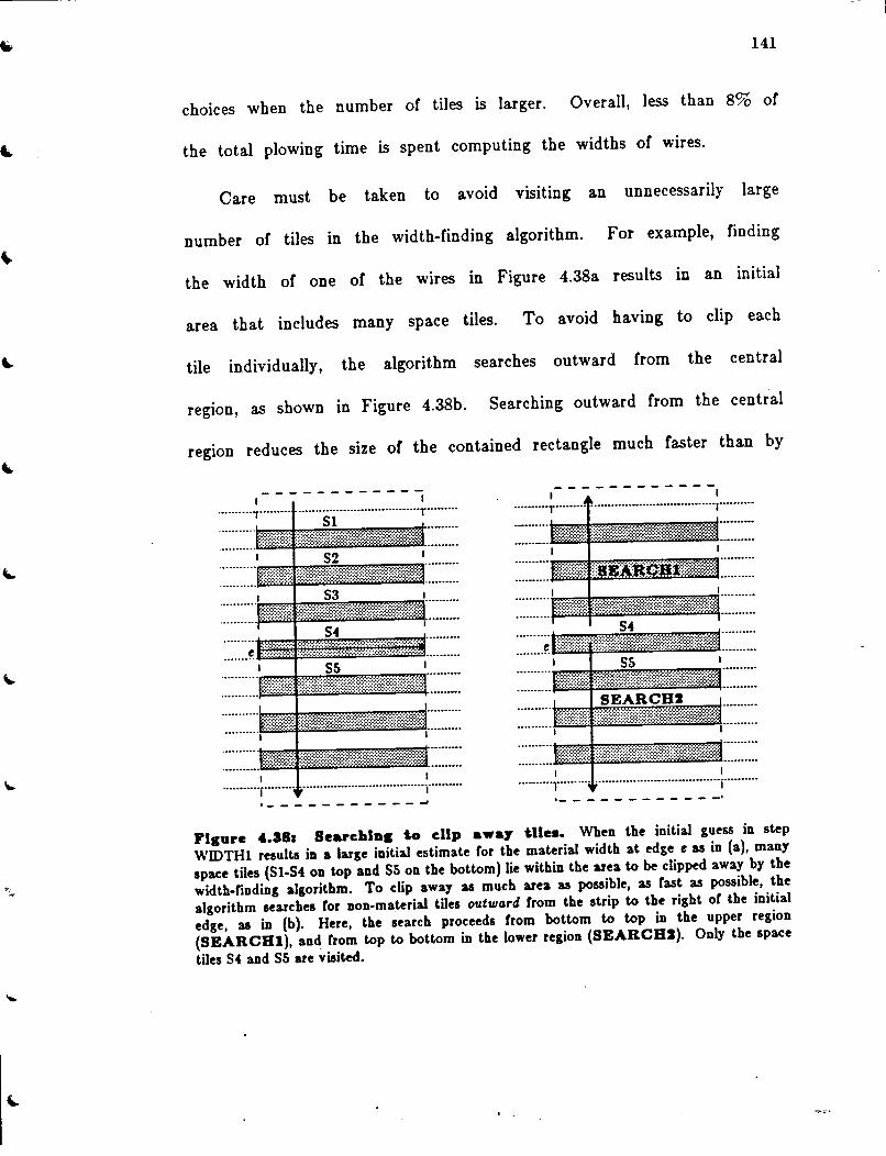
141
choices when the number of tiles is larger. Overall, less than 8% of
the total plowing time is spent computing the widths of wires.
Care must be taken to avoid visiting an unnecessarily large
number of tiles in the width-finding algorithm. For example, finding
the width of one of the wires in Figure 4.38a results m an initial
area that includes many space tiles. To avoid having to clip each
tile individually, the algorithm searches outward from the central
region, as shown in Figure 4.38b. Searching outward from the central
regiOn reduces the size of the contained rectangle much faster than by
I ............ , ......... , ............................. -----··-r·········
Sl
S2 I
,,,,,,,,,,,,,,,.,
.••••••••• 1 S3 J
···-------, S4
I
e :::::::::I ss I
c;:;:·:·:::;:':·:·:
•••••••••• 1 I .••••••••• 1 I
I I I
I I -----------.-······--:1.::····································-,···········
·-----------~ ·- - - - - - - - - - - -· Figure 4.381 Searehlag to ellp awa7 tllea. When the initial guess in step
WIDTH! results in a large initial estimate for the material width at edge e as in (a), many
space tiles (Sl-S4 oo top and S5 oo the bottom) lie within the area to be clipped away by the
width-finding algorithm. To clip away as much area as possible, as fast as possible, the
algorithm searches ror non-material tiles outward rrom the strip to the right or the initial
edge, as io (b). Here, the search proceeds from bottom to top in the upper region
(SEARCBl), and from top to bottom in the lower region (SEARCB2). Only the space
tiles S4 and S5 are visited.
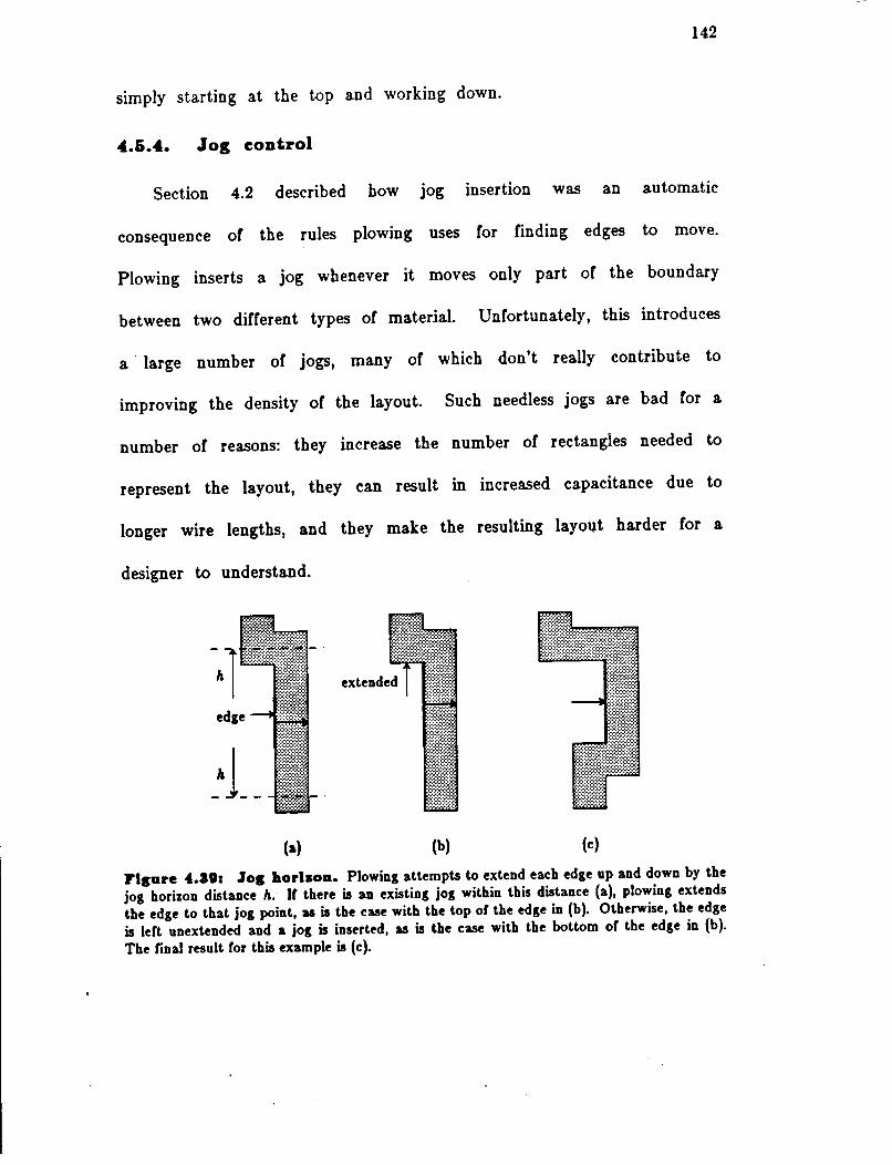
142
simply starting at the top and working down.
4.6.4. Jog control
Section 4.2 described how Jog insertion was an automatic
consequence of the rules plowing uses for finding edges to move.
Plowing inserts a jog whenever it moves only part of the boundary
between two different types of material. Unfortunately, this introduces
a large number of jogs, many of which don't really contribute to
improving the density of the layout. Such needless jogs are bad for a
number of reasons: they increase the number of rectangles needed to
represent the layout, they can result m increased capacitance due to
longer wire lengths, and they make the resulting layoQ.t harder for a
designer to understand.
extended
(a) (b) (c)
Flsure 4.31: Jos horlsoa. Plowing attempts to extend each edge up and down by the
jog horizon distance h. Ir there is an existing jog within this distance (a), plowing extends
the edge to that jog point, as is the case with the top or the edge in (b). Otherwise, the edge
is ldt unextended and a jog is inserted, as is the case with the bottom or the edge in (b).
The final result ror this example is (c).
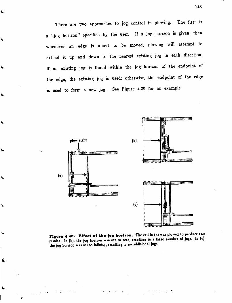
~ 143
'
There are two approaches to jog control in plowing. The first is
a "jog horizon" specified by the user. If a jog horizon is given, then
whenever an edge is about to be moved, plowing will attempt to
extend it up and down to the nearest existing jog in each direction.
If an existing jog is found within the jog horizon of the endpoint of
the edge, the existing Jog 15 used; otherwise, the endpoint of the edge
is used to form a new jog. See Figure 4.39 for an example.
1':::·:·:·:·:·:;:·:·:·:·:;:·:;:;:;:;:: :'i::;:;:;:·:;:·:·:;:;:·:·:·:·:<·:·:·:·:···:·:·:·:·:·:·:
I :ij'jl I :•.
plow right
~o;.;:;.;.;-;.;.;:::;.;.;.;.;:;:;::::::~::::;:;:;.;.;::: •. ;.;:;.;:;.;.;.;.;.;-;.;.;.;.:·:·:·
(a) ~ _.. ~
II (c)
r:::·:;:·:·.;:::;:;:·:::::;:·:;:;:;::: .1'-(1:·:·: :;:·:::·:;:;:;:·:·:·:·:·:·:·:·:·.·:·:·:·:·:·:·
Flsure 4.40a Efted of the Jos horlaoa. The cell in (a) was plowed to produce two
results. In (b), the jog horizon was set to zero, resulting in a large number or jogs. In (c),
the jog horizon was set to infinity, resulting in no additional jogs.

144
The two extreme values of the jog horizon best explain its effect
on plowing. When the jog horizon 1s set to zero, plowing will insert
jogs freely everywhere it wants to. This strategy results in the
smallest pitch attainable by plowing, but a large number of jogs.
When the horizon is set to infinity, plowing will never insert a jog
unless required to do so to prevent a layout-rule violation. The result
is a smaller number of jogs, but a potentially larger pitch. See
Figure 4.40 for an example. In the worst case, no compaction will be
possible unless jogs can be inserted, as was illustrated in Figure 4.6 in
Section 4.1.8.
An alternate approach to jog reduction is to insert them into a
layout freely, and then attempt to straighten them out after the plow
has finished. Jogs should only be eliminated if doing so doesn 'i cause
any additional geometry to move. This can be accomplished best by
pulling the jogs in the opposite direction to the one in which the
plow moved, as described in Figure 4.41.
This alternate approach makes use of the same fundamental
operation as plowing, namely searching for other edges to move as a
result of moving a given edge. During jog reduction, this search lS
performed for the edges of each jog that is a candidate for being
eliminated. U eliminating the jog causes no new edges to move, the
jog is eliminated; otherwise, it is left alone.

145
-------1
(a) (b) (c)
------i
-----_I ______ J
(d) (e) (r)
Flsure 4.411 Jos cleanup. Plowing the layout in (a) results in the jogs in (b). These
can be eliminated by a post-pass that works from right to left. Starting at the right-band
side or the area affected by plowing, search Cor edges with material on their LHS and space
on their RHS (c). If such edges belong to a jog that can be "nipped" to reduce the number
or jogs, and if moving this jog causes no other edges to move, nip the jog (d). When nipping
a jog, both edges or the jogged material are moved at the same time. Continue the search
lertward from the LHS or the material round in the previous search (e), nipping any jogs
round in that step as well (r).
Function Lines
Main loop, mise:: 2900
Rules: 2SOO
Searchin&: 1300
Jog reduction: 750
Width computation: 550
Plowing four directions: 600
Technology independence: goo
Total: 9SOO
Table 4.11 Plowlas code •lae. This table shows how many lines or code are in each
or the major components or pJowin&. By rar the dominant portion or the basic plowing
algorithm are the rules and search procedures.

'
146
4.1. Measurement and evaluation
The implementation of plowing in Magic consists of Q,500 lines of
"C" code, divided according to function as shown in Table 4.1. This
division reflects the difficulty of implementing the various pieces of the
algorithm. There is a large amount of code devoted to recognizing
features from the layout-the plowing rules, width computation, and
search procedures all do this. This code 15 probabbly more complex
than the corresponding code in symbolic compactors. I believe the
extra complexity is because plowing works directly on physical masks:
it has more freedom over what geometry it moves than a traditional
compactor, and so must be correspondingly more cautious.
Although plowing has other uses as well, it can be used as an
effective compactor. Table 4.2 presents the result of using plowing to
compact the cells m a suite composed by Wayne Wolf for evaluating
the behavior of Lava, a one-dimensional critical-path compactor
[Wol85].
Three different sets of numbers for plowing appear in the table.
The first, for plowing with no jog introduction, show that in most
cases the inability to introduce jogs severely limits the amount of
compaction possible. This is in kee-ping with the reasons given m
Section 4.1.8, namely that vertical wires can prevent geometry from
moving to take up slack on the opposite side if the wire is unable to

'
147
Plowing
Cell Lava (no jogs) (raw) (merged)
pitch pitch % pitch % pitch %
alu 77 100 +30 87 +13 81 +5
aluw 67 201 +200 69 +3 56 -16
bg 23 27 +17 23 0 23 0
bg2b 27 38 +41 28 +4 28 +4
cbo 82 89 +9 68 -17 68 -17
cbox 69 239 +246 73 +6 67 -3
cereg 58 77 +33 58 0 58 0
clam reg 194 223 +15 184 -5 184 -5
cmid 101 136 +35 106 +5 gg -2
count 27 45 +67 36 +33 25 -7
countx 23 60 +161 44 +91 29 +26
enc 142 159 +12 132 -7 132 -7
plain 15 27 +80 23 +53 15 0
shift2 35 36 +3 32 -9 32 -9
shift2x 37 44 +19 28 -24 28 -24
Table 4.t: Plowla• aaed - a compac~or. This table compares plowing with the
Lava compactor, using examples provided by Wayne Wolf. The goal was to minimize the z
dimension or each cell. In the plowing examples, the plow was placed at the left-hand side or
each cell and pushed to the right. Three results are shown Cor plowing. The first is with jog
insertion disabled; the last two two are with jog insertion enabled. The "raw" plowing
column gives the results or plowing Wolrs example cells as they were provided; the "merged"
column is Cor plowing these cells after the modifications described in the text. The "%"
column shows the percentage difference in the z-dimension relative to Lava. All of the
plowing examples took less than 8 seconds or CPU time on a V AX-11/780. See [Wol85J Cor a
description or the cells used.
bend.
Better results are possible with jog introduction, as the two
remaining columns show. The "raw" column gtves the resulting x-
dimensions of each cell when plowing was run on the unaltered cells
from the test suite. Unfortunately, two sorts or constructs in these
cells prevented plowing from achieving as much compaction as possible;
these are illustrated in Figure 4.42. These point out a deficiency in
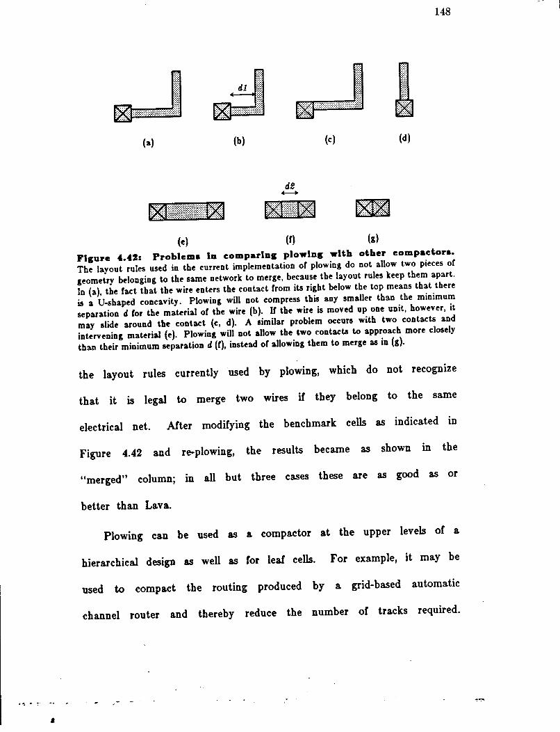
.. ~ . ~ -·
'
148
I . . (a) (b) (c) (d)
de -(e) (f) (g)
Figure 4.4Z: Problem• Ia eomparlag plowlag with other eompaeton.
The layout rules used in the current implementation of plowing do not allow two pieces of
geometry belonging to the same network to merge, because the layout rules keep them apart.
In (a), the fact that the wire enters the contact from its right below the top means that there
is a U-shaped concavity. Plowing will not compress this any smaller than the minimum
separation d for the material of the wire (b). If the wire is moved up one unit, however, it
may slide around the contact (c, d). A similar problem occurs with two contacts and
intervening material (e). Plowing will not allow the two contacts to approach more closely
than their minimum separation d (f), instead or allowing them to merge as in (g).
the layout rules currently used by plowing, which do not recognize
that it is legal to merge two wires if they belong to the same
electrical net. Arter modifying the benchmark cells as indicated in
Figure 4.42 and re-plowing, the results became as shown m the
"merged" column; in all but three cases these are as good as or
better than Lava.
Plowing can be used as a compactor at the upper levels of a
hierarchical design as well as for lear cells. For example, it may be
used to compact the routing produced by a grid-based automatic
channel router and thereby reduce the number of tracks required .

149
Jog horizon Time Height Improvement
0 2:20 139 11.5%
infinite 1:50 150 4.5%
Table 4.3: Plowlns a routing channel. This table shows the result or plowing the
routing for Deutsch's Difficult Example, produced by Magic's channel router, to reduce its
height. The initial height or the channel was 157 units, corresponding to 20 routing tracks.
Table 4.3 shows the result of compacting the routing produced for
Deutsch's Difficult Example by Magic's channel router [Ha084]. The
results of plowing both with and without jog introduction are shown.
With jog introduction disabled, the result is larger but more regular,
and compaction is slightly faster because the layout does not become
so highly fragmented.
As an even larger example, plowing was used to modify the
position of one of the cells lD the fioorplan of a 8,000-transistor,
nMOS chip. The fioorplan cell was 3900 units square, and contained
19 subcells. The subcell being moved had a total of 30 wires
attached to it, and was moved distances of between 200 and 300
units. Each plow in this example required between approximately 1
minute of CPU time on a VAX-11/780,
The run times reported for the above examples are likely to be
worst-case for plowing, since in all of them an entire cell was being
plowed. More typically, plowing is used to make local changes, so
less of a cell is modified and plowing takes less time. For example,
most plows to the 16-transistor cell shown in Figure 4.43 take only 1
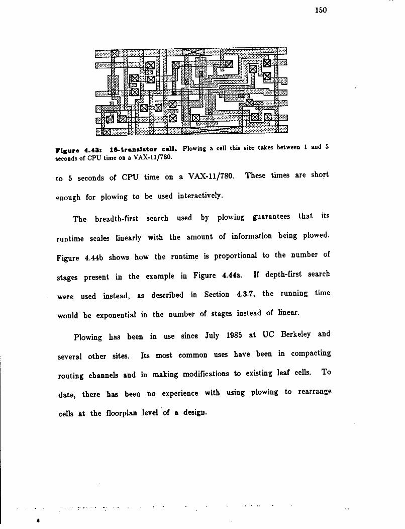
150
·I:{{
t-: -. ""-·1S;J : )(.! .
!. -:::::.
-:IXJ _:
Flsure 4.43a 11-baa•ldor cell. Plowing a cell this size takes between 1 and 5
seconds or CPU time on a V AX-11/780.
to 5 seconds of CPU time on a V .AX-11/780. These times are short
enough for plowing to be used interactively.
The breadth-first search used by plowing gUarantees that its
runtime scales linearly with the amount of information being plowed.
FigUre 4.44b shows how the runtime is proportional to the number of
stages present in the example in FigUre 4.44a. If depth-first search
were used instead, as described in Section 4.3.7, the running time
would be exponential in the number of stages instead of linear.
Plowing has been in use· since July 1Q85 at UC Berkeley and
several other sites. Its most common uses have been in compacting
routing channels and in making modifications to existing leaf cells. To
date, there has been no experience with using plowing to rearrange
cells at the fioorplan level of a design.

(a)
(b)
70
60
so
40 Seconds
30
20 ;'
10 l f.
.!'
............
500 1000 Number or Stages
one stage
151
1500
Flsure 4.44a Linear srowt.h of plowlns'• runtime. The graph in (a) plots the
time in seconds (on a V AX-11/785) taken to plow Nor the stages present in (b).
4.7. Limitations and areas for further work
4.7 .1. Global considerations
The plowing algorithm is built atop a collection of rules that find
new edges to move as a result of moving a given edge. This style of
approach is well-suited to local optimization, but does not easily
incorporate global information. For example, it is easy for plowing to

152
pack geometry as close to its neighbors as possible. On the other
hand, it lS difficult for plowing to perform global wire-length
minimization. This latter optimization may require increasing the
lengths of individual w1res m order to make reductions in the lengths
of others possible, so there lS no consistent local improvement that will
yield the global optimum.
Another example where purely local considerations were insufficient
was seen m the comparison between plowing and Lava in the previous
section. Because plowing had no direct way of knowing when two
pieces of geometry are connected, it unnecessarily kept electrically
equivalent pieces of geometry from being merged. One way in which
this might be corrected would be to use the algorithms for tracing
node connectivity described in Chapter 3 to identify equh:alent nodes
during plowing.
·-------: I 9:
:181 w I------ _I
(a)
-----I a'
li!!lJ I
•• I I
•II L.----·
(b)
,-------, •ri 81 Ill• •-------·
(c) (d)
Flsure 4.4&a Jos• eaa llml\ eompadloa Ia \he perpeadleular dlree\loaa.
If a jog is introduced in (a) to obtain better .z-compac:tion (b), the resulting y-compac:tion (c)
becomes limited in a way that it would not have been had no jog been introduced (d). In
this example, the resulting area is smaller in (d), with no jogs, than it is in (c) with a jog.

,
153
4.7.2. Jog introduetion
Jogs are an example where strictly local analysis can in fact be
harmful. While plowing is able to introduce jogs as needed locally,
this is not always the best possible strategy if one wishes to reduce
the overall area of a cell. Introducing jogs in one dimension often
makes compaction in the perpendicular dimension more difficult. This
can be seen in the example in Figure 4.45. The consequence IS to
reduce still further the usefulness of automatic Jog insertion by
plowing. In fact, most users will usually leave the jog horizon set to
infinity to prevent any new jogs from being introduced by a plow
operation.
At first it might seem that if jog insertion is of so little use, it
should be removed from the plowing algorithm entirely. However,
sliver
...
(a) {b)
l'lsure 4.4th SliTer• can occur eYeD without Jos Introduction. Slivers can
be introduced wherever plowing creates new horizontal edges, not just when it introduces
jogs. Hence, even if plowing introduced no jogs, it would still be necessary to have rules to
avoid introducing slivers. For example, when the edge e shown in (a) slides to the right, it
leaves a sliver behind even though no jogs were introduced (b).

154
very little is to be gained by doing this. None of the plowing rules
become any simpler if no new jogs are inserted by plowing. For
example, sliver elimination is still required to handle the cases such as
that shown in Figure 4.46. ,Furthermore, the flexibility of the plowing
algorithm is reduced in the fraction or cases where jog introduction is
desirable.
I believe a. more useful approach would be to exerciSe more
selectivity in the way jogs are introduced, by giving consideration to
compaction in the perpendicular direction when creating a jog. A
good way or doing this might be to apply a. set or heuristic rules,
such as those used by Wolf m Supercompa.ction [Wol84), that examme
patterns or geometry around potential jog points to determine whether
a jog is a good one or a bad one.
4. 7 .3. Heuristic plowing rules: dimculty or testing
The third problem with plowing is a consequence of it basing it
on a collection of heuristic rules for determining when new edges have
to move. These rules are probably the single most difficult part of
the plowing algorithm. Considerably more of the plowing a.lg~rithm is
devoted to applying these rules than, for example, is spent building
the constraint graph in a typical critical-path compactor. Furthermore,
although each rule is fairly simple, choosing a. small collection of rules
that covers all eventualities requires much careful thought. I believe

....
155
the net effcd lS to make plowing more difficult to implement correctly
than a traditional compactor.
In fact, because of this diffic1Jlty, testing is particularly important
to ensure that an implementation of plowing is correct. The current
implementation performs this testing on a collection of benchmark cells
by randomly generating hundreds of thousands of plows, plowing, and
then testing to see that connectivity, transistor and contact sizes, and
design-rule correctness have all been preserved. (In fact, it uses the
circuit extractor to verify the first two properties). The successful
results of this testing give me a high degree of confidence that the set
of rules described in this chapter lS sufficient to preserve those
properties plowing is intended to preserve .
156
Chapter 6
Conclusions
6.1. Summaq
This thesis has presented two complementary tools for speeding the
debug cycle for custom integrated circuits: a fast, incremental, and
hierarchical circuit extractor, to convert the layout into a form that
can be simulated, and a plow operation, to facilitate making changes
to a layout. These two tools have substantially eliminated circuit
extraction and layout modification from the critical path in the debug
cycle. Instead, the dominant component is now debugging-actually
discovering new bugs via simulation, timing verification, or other forms
of analysis-instead or the overhead or preparing for simulation, as m
the past.
Chapter 3 presented a. hierarchical and incremental circuit
. extractor. The structure of the circuit it produces parallels that of
the original layout, so this structure can be exploited by the tools
that read the extracted circuit. The extractor is incremental, so it
avoids having to re-extract the entire circuit after each change to the
layout.

~ 157
Two new algorithms form the core of this extractor. The fiat
extractor presented in Section 3.2 uses an algorithm based on tile
flooding. Corner-stitching makes flooding a practical choice because it
stores features, not pixels, and hence both the memory requirements
and the extraction cost per circuit element are small. The stitches
make it possible to find neighboring tiles simply by following a list or
pointers, so flooding a node in a corner-stitched plane is very fast.
The hierarchical extraction algorithm allows nearly arbitrary
overlap between cells while still preserving the original hierarchical
structure in its output. Because it is hierarchical, it takes advantage
of regular structures such as arrays to run very fast. Where cells
overlap or abut, it adjusts parasitic resistance and capacitance.
Because transistors are not allowed to be created or destroyed by
overlap, all adjustments are strictly additive, and so can be stored as
additive adjustments to the circuit of the parent of the overlapping or
abutting cells. As a result, subcell circuits don't have to be re
extracted when their parents change; only the changed cells and their
ancestors must be re-extracted during incremental extraction.
Overall, the extractor demonstrates three important ideas. First,
corner-stitching is ·well-suited for use in a circuit extractor. Its ability
to find adjacent mask information is critical to the speed or the basic
extractor, and its ability to search areas is responsible for the speed of
'
158
the hierarchical extractor. Second, incremental extraction significantly
reduces the amount of time required to re-extract a layout after it has
been modified. Finally, hierarchical extraction can be made to work
with minimal restriction of the kinds of overlaps available to the
designer.
Chapter 4 presented plowing, a powerful new operation for
manipulating mask-level layout. Plowing allows a designer to move
one piece or a layout and have the rest or the layout move
automatically to preserve layout-rule correctness and connectivity. This
ability leads to a different style of design than previous symbolic or
procedural/textual systems: the designer manipulates only a single
representation, instead of using a compactor to convert between
symbolic or textual representation and mask-level layout. The result is
both greater predictability and more designer control.
The plowing algorithm presented in Section 4.3 is novel in several
respects. Its overall framework is similar to critical-path compaction,
but instead of building a constraint graph, plowing works directly on
the layout. The fundamental step in plowing is moving a single edge
in the layout. The algorithm uses rules to determine whether moving
this edge causes others to move.- In effect, these rules are
"computing" the arcs in a constraint graph as the plowing algorithm
progresses, even though no graph is built explicitly. Plowing makes

159
use of shadow search and outline search, both new and efficient
searching procedures based on corner-stitching, resulting in very fast
rule application. By processing edges in breadth-first order and
working directly from a corner-stitched layout, the algorithm has
running time linear in the number of edges it processes.
Plowing has several practical uses. When used as a 1-d
compactor, by placing the plow to one side of a cell and plowing all
the way to the opposite side, it produces layouts with pitches
comparable to those produced by other good 1-d compactors. When
used to move around mask geometry in leaf cells, plowing is fast
enough to be used interactively: most plows take 5 seconds or less on
a VAX-11/780.
6.2. Lessons learned
In addition to presenting two tools that change the character of
the debug cycle for custom ICs, I believe that this dissertation
demonstrates two overall lessons on how to build computer-aided design
tools that manipulate geometric layout.
First, corner-stitching is a good, single representation for building
these tools. Plowing and circuit extraction are examples of two very
different operations that nonetheless share some basic geometric
operations: detEcting adjacency, searching areas or shadows, and tracing
160
outlines. Because these underlying operations are well-supported by
corner-stitching, both tools can avoid the overhead of building their
own structures m addition to the corner-stitched planes used to store
layout. A single corner-stitched representation also makes it easy to
integrate both tools m the same layout editor, with attendant
advantages of code sharing and simplicity.
The second lesson is that incremental approaches can significantly
improve the performance of CAD tools, particularly as designs become
increasingly large. This thesis focused on incremental circuit
extraction, demonstrating that it was possible to re-extract a 40,000
transistor chip in 5 minutes incrementally, versus 20 minutes if the
entire chip were re-extracted. Speedups of this magnitude, or even
greater ones if the ideas discussed in Section 4.6.3 are used, may also
be applied to other problems, such as fault location, netlist comparison,
etc. The key to an incremental approach is partitioning the problem
in such a way that small changes to the input result in changes to
only a small part or the output.
6.3. Looking forward
Several areas remain for further work on both the circuit
extractor and plowing. Chapter 4 mentioned several potential
inaccuracies or the circuit extractor, particularly with regard to the

161
way it computed node resistances. An attempt should be made to
quantify these and see how much of a difference they make to the
result of circuit simulation or timing verification.
From the opposite direction, the hierarchical adjustments made to
resistance and capacitance may well make only an insignificant
difference m overall node resistance and capacitance, particularly when
the amount of overlap between cells is small. In some examples
already measured, these adjustments make less than a 5% difference in
the critical paths found during timing analysis, although more careful
study is required. If it is possible to ignore hierarchical adjustments
in most cases, it should be possible at least to double the speed of
the hierarchical extractor.
It may be possible to incorporate additional rules into plowing to
improve the quality of the jogs it introduces. · Also, it is probably
worthwhile to investigate alternate collections of plowing rules, to see
if there is a smaller and simpler set that accomplishes the same result
as those currently being used.
Finally, both plowing and circuit extraction have proven rich in
new algorithms. These have potential for use as components of other
tools. For example, a combination of the algorithms used for node
finding and coupling capacitance detection can be used for identifying
certain potential faults in ICs, such as shorts between parallel or

162
overlapping w1res. The shadow search algorithm can form the basis
for a gridless Lee-style router. The ability to trace connectivity can
be used during design-rule checking to filter out spacing violations
between connected geometry.

..
163
Bibliography
[AGR70J S. B. Akers, J. M. Geyer and D. L. Roberts, "Integrated
Circuit Mask Layout with a Single Conductor Layer",
Proceedings of the 7th Design Automation Conference, 1970,
7-16.
[Arn85) M. H. Arnold, "Corner-Based Layout Rule Checking for
VLSI Circuits.", Ph.D. Thesis, University of California,
Berkeley, CA., 1985.
[Bak80) C. Baker, "Artwork Analysis Tools for VLSI Circuits",
Masters Thesis, MIT, 1980.
[BaT80] C. M. Baker and C. Terman, "Tools for Verifying
Integrated Circuit Designs", Lambda Magazine, 4th quarter
1980, 22-30.
[Bal82) M. Bales, "Layout Rule Spacing of Symbolic IC Artwork",
UCB/Electronics Research Lab. M82/72, Electronics Research
Lab of U. of CA at Berkeley, May 1982.
[BHE83) J. D. Bastian, C. E. Huang, M. Ellement, L. P. McNamee
and P. J. Fowler, "Symbolic Parasitic Extractor for Circuit
Simulation (SPECS)", Proceedings of the eoth Design
Automation Conference, 1983, 346-352.
[BMS81] J. Batali, N. Mayle, H. Shrobe, G. Sussman and D. Weise,
"The DPL/Daedalus Design Environment", in VLSI '81,
Academic Press, 1981, 183-192.
(BoW83} D. G. Boyer and N. Weste, "Virtual Grid Compaction Using
the Most Recent Layers Algorithm", Proceedings of the
IEEE International Conference on Computer-Aided Design
(ICCAD}, September 1983, 92-93.
[Bry81) R. E. Bryant, "MOSSIM: A Switch-Level Simulator for MOS
LSI'', Proceedings of the 18th Design Automation
Conference, June 1981, 786-790.
(CHY80] S. P. Chao, Y. S. Huang and L. M. Yam, "A Hierarchical
Approach for Layout vs Circuit Consistency Check",
Proceedings of the 17th Design Automation Conference,
1980, 270-276.
[Clfl(83} N. Chen, C. Hsu and E. Kuh, "The Berkeley Building-Block
Layout System for VLSI Design", Electronics Research Lab.
Memo, Electronics Research Lab., Univ. of CA at Berkeley,
.,~.·
(da84)
164
February 14, 1983.
J. M. da Mata, "ALLENDE: A Procedural Language for the
Hierarchical Specification of VLSI Layouts", Draft,
Department of EECS, Princeton University, 1984.
[DoL85) J. Doenhardt and T. Lengauer, "Algorithmic Aspects of
One-Dimensional Layout Compaction", Bericht Nr. 23, Reihe
Theoretische Informatic, University of Paderborn, West
Germany, February 1985.
[Dun78) A. Dunlop, "SLIP: Symbolic Layout of Integrated Circuits
with Compaction", in Computer-Aided Design, vol. 10 ,
Nov. 1978, 387-391.
[Dun80) A. E. Dunlop, "SLIM-The Translation of Symbolic Layouts
into Mask Data", Proceedings of the 17th Des£gn
Automation Conference, 1980, 595-602.
[Fit82) D. T. Fitzpatrick, "MEXTRA: A Manhattan Circuit
Extractor", Electronics Research Lab. Memo M82/42,
Electronics Research Laboratory, University of California,
Berkeley, January 1982.
(Fit83] D. T. Fitzpatrick, "Exploiting Structure in the Analysis of
Integrated Circuit Artwork", UCB/Computer Science Dpt.
83/130, Computer Science Division (EECS), University of
California, Berkeley, August 1983.
[GiN77) D. Gibson and S. Nance, "A Symbolic System for Circuit
Layout and Checking", Proceedings of the IEEE· Symposium
on Circuits and Systems, 1977, 436-440.
(GuH82) A. Gupta and R. W. Hon, "HEXT: A Hierarchical Circuit
Extractor", CMU, Carnegie-Mellon University, Pittsburgh,
PA-CS-82-147, December 15, 1982.
(Gup83) A. Gupta, "ACE: A Circuit Extractor", Proceedings of the
20th Design Automation Conference, 1983, 721-725.
(Ha084) G. T. Hamachi and J. K. Ousterhout, "A Switchbox Router
with Obstacle Avoidance", Proceedings of the 21st Design
Automation Conference, June 1984, 173-179.
(Hsu79) M. Y. Hsueh, Symbolic Layout and Compaction of
Integrated Circuits, University of California at Berkeley
Electronics Research Lab., Dec. 1979.
(JoB80] S. Johnson and S. Browning, "The LSI Design Language i",
Internal Technical Memorandum 1980-1273-10, Bell
Laboratories, November 18, 1980.
(Jou84] N. P. Jouppi, "Timing Verification and Performance
Improvement of MOS VLSI Designs", Report No. 84-266

[Jou85]
[KeN82a]
[KeN82b]
[Kin84]
[KKY79]
[Lar71]
(Lar78]
[LeM85]
[LeS82]
(LeM84]
(Ph.D. Thesis), Stanford University, Palo Alto, Ca., 1984.
N. Jouppi, Personal Communication, January 1985.
165
K. Keller and A. Newton, "KIC 2: A Low-Cost, Interactive
Editor for Integrated Circuit Design", lD Proc. 24th
COMPCON, Feb. 1982.
K. Keller and A. Newton, "A Symbolic Design System for
Integrated Circuits", in Proc. 19th Design Automation
Conference, June 1982.
C. Kingsley, "A Hierarchical, Error-Tolerant Compactor",
Proceedings of the 21st Design Automation Conference,
1984, 126-132.
A. Kishimoto, H. Kawanishi, H. Y oshizawa, H. Ohno, Y.
Fujinami and K. Kani, "An Interconnection Check Algorithm
for Mask Pattern", ISCAS Conference, 1979, 669-672.
R. P. Larsen, "Computer-Aided Preliminary Layout Design of
Customized MOS Arrays", IEEE Transactions on Computers
C-20, 5 (May 1971), 512-523.
R. P. Larsen, "Versatile Mask Generation Techniques for
Custom Microelectronic Devices", Proceedings of the 15th
Design Automation Conference, June 1978, 193-198.
C. E. Leiserson and F. M. Maley, "Algorithms for Routing
and Testing Routability of Planar VLSI Layouts",
Proceedings of the 17th Annual ACM Symposium on the
Theory of Computing (Annual ACM Symp. on Theory of
Computing), May 1985.
E. Lelarasmee and A. Sangiovanni-Vincentelli, "RELAX: A
New Circuit Simulator for Large Scale MOS Integrated
Circuits", Memo. Electronics Research Lab.-M82/6, UC
Berkeley Electronics Research Lab, Berkeley, .CA, February
1982.
T. Lengauer and K. Mehlhorn, "The HILL System: A Design
Environment for the Hierarchical Specification, Compaction,
and Simulation of Integrated Circuit Layouts", Proceedings
of the MIT Conference on Advanced Research in VLSI,
Cambridge, MA, 1984, 139-148.
(LiW83] Y. Liao and C. K. Wong, "An Algorithm to Compact a
VLSI Symbolic Layout with Mixed Constraints", IEEE
Transactions on CAD of Integrated Circuits and Systems
CAD-2, 2 (April 1983), 62-69.
(Lie78] H. Lieberman, "How to Color in a Coloring Book",
Computer Graphics 12, 3 (August 1Q78), 111-116.
166
[LNS82] R. Lipton, S. North, R. Sedgewick, J. Valdes and G.
Vijayan, "ALI: A Procedural Language to Describe VLSI
Layouts", Proceedings of the 19th Design Automation
Conference, 1Q82, 467-475.
[Mal85] F 0 M. Maley, "Compaction with Automatic Jog
Introduction", Proceedings of the 1985 Chapel Hill
Conference on VLSI, Chapel Hill, NC, May 1Q85, 261-284.
(MNE82] R. Mathews, J. Newkirk and P. Eichenberger, "A Target
Language for Silicon Compilers", Compcon Proceedings,
Spring 1Q82, 34Q-353.
[McC84] S. P. McCormick, "EXCL: A Circuit Extractor for IC
Designs", Proceedings of the £1st Design Automation
Conference, 1Q84, 624-628.
[MCT80] T. Mitshuhashi, T. Chiba, M. Takashima and K. Yoshida,
"An Integrated Mask Artwork Analysis System", Proceedings
of the 11th Design Automation Conference, 1Q80, 277-284.
(Mor84) H. Mori, "Interactive Compaction Router for VLSI Layout",
Proceedings of the £1st Design Automation Conference,
1Q84, 137-143.
(Mos81] R. C. Mosteller, "REST: A Leaf Cell Design System", in
VLSI81, J. P. Gray (editor), Academic Press, 1Q81, 163-172.
[NaP73) L. W. Nagel and D. 0. Pederson, "SPICE (Simulation
Program with Integrated Circuit Emphasis)", Electronics
Research Laboratory Memorandum No. Electronics Research
Lab.-M382, University of California, Berkeley, April 12, 1Q73.
[NeS83) B. J. Nelson and M. A. Shand, "An Integrated, Technology
Independent, High Performance Artwork Analyzer for VLSI
Circuit Design", Technical Report VLSI-Tech. Rep.-83-4-1,
VLSI Program, Division of Computing Research, CSIRO,
Eastwood, SA 5063, Australia, April 1Q83.
[NeF82) M. K Newell and D. T. Fitzpatrick, "Exploiting Structure
in Integrated Circuit Design Analysis", Proceedings of the
Conference on Advanced Research in VLSI, MIT, :MIT,
Boston, Mass., January 1Q82.
(Ous81) J. Ousterhout, "Caesar: An Interactive Editor for VLSI
Layouts", VLSI Design II, 4 (Fourth Quarter 1Q81).
[OuU82] J. K. Ousterhout and D. M. Ungar, "Measurements of a
VLSI Design", Proceedings of the 19th Design Automation
Conference, 1Q82, Q03-Q08.
(Ous83) J. K. Ousterhout, "Crystal: A Timing Analyzer for nMOS
VLSI Circuits", 9rd Caltech Conference on Very Large Scale

' ,
[Ous84a)
(Ous84b]
(OHM85)
(Pav81)
(RSS85]
(RBD83)
(SaK82)
(SaP83)
(Sch81)
(SLM83]
(Sco84)
(SHM85)
(Smi7Q)
167
Integration, Pasadena, CA, March 21-23, 1Q83, 57-70.
J. Ousterhout, "Corner Stitching: A Data-Structuring
Technique for VLSI Layout Tools", IEEE Transactions on
CAD/ICAS CAD-9, 1 (January 1Q84).
J. K. Ousterhout, "Switch-Level Delay Models for Digital
MOS VLSI", Proceedings of the e1st Design Automation
Conference, 1Q84, 542-548.
J. K. Ousterhout, G. T. Hamachi, R. N. Mayo, W. S. Scott
and G. S. Taylor, "The Magic VLSI Layout System", IEEE
Design and Test of Computers e, 1 (February 1Q85}, lQ-30.
T. Pavlidis, "Contour Filling in Raster Graphics", Computer
Graphics 15, 3 (August 1Q81), 2Q-36.
P. S. Reineke, R. D. Skinner, M. C. Swanson and D. A.
Winkelmann, STAWS 1985: A Report on the Integrated
Circuit Industry, Integrated Circuit Engineering Corporation,
1Q85.
J. Rosenberg, D. Boyer, J. Dallen, S. Daniel, C. Poirier, J.
Poulton, D. Rogers and N. Weste, "A Vertically Integrated
VLSI Design Environment", Proceedings of the eoth Design
Automation Conference, 1Q83, 31-38.
S. Sastry and S. Klein, "PLATES: A Metric-Free VLSI
Layout Language", Conference on Advanced Research in
VLSI, 1Q82, 165-174.
Sastry and Parker, 1Q83.
L. K. Scheffer, "A Methodology for Improved Verification of
VLSI Designs Without Loss of Area", 2nd Caltech
Conference on VLSI, January 1Q81, 2QQ-300.
M. Schlag, F. Luccio, P. Maestrini, D. T. Lee and C. K.
Wong, "A Visibility Problem in VLSI Layout Compaction",
RC Q8Q6, ffiM T.J. Watson Research Center, 1Q83.
W. S. Scott, Technology Independent Layout Representation
in Magic, Master's Report, University of California, Berkeley,
December 1Q84.
W. S. Scott, G. Hamachi, R. N. Mayo and J. Ousterhout,
editors. "1Q85 VLSI Tools: More Works by the Original
Artists", Report No. UCB/Computer Science Opt. 85/225,
Computer Science Division (EECS), University of California,
Berkeley, February 1Q85.
A. R. Smith, "Tint Fill", Computer Graphics 19, 2 (August
1Q7Q), 276-283.
168
(Spi83) R. L. Spickelmier, "Verification of Circuit Connectivity",
UCB/Electronics Research Lab. M83/66, Electronics Research
Laboratory, University of California, Berkeley, October 1Q83.
(TMC82} M. Takashima, T. Mitsuhashi, T. Chiba and K. Yoshida, "A
Program for Verifying Circuit Connectivity of MOS/LSI
Mask Artwork", Proceedings of the 1fJth Design Automation
Conference, 1Q82, 544-550.
(TaH83] G. Tarolli and W. J. Herman, "Hierarchical Circuit
Extraction with Detailed Parasitic Capacitance", Proceedings
of the 20th Design Automation Conference, 1Q83, 337-345.
[Ta084] G. S. Taylor and J. K. Ousterhout, "Magic's Incremental
Design-Rule Checker", Proceedings of the 21st Design
Automation Conference, Albuquerque, NM, June 1Q84, 160-
165.
[Ter83) C. Terman, "ESIM Reference Manual", in Berkeley VLSI
Tools, R. N. Mayo, J. K. Ousterhout and W. S. Scott
{editor}, 1Q83.
[The78] A. Thesen, in Computer Methods in Operations Research,
Academic Press, 1Q78.
(Tri81) S. Trimberger, "Combining Graphics and a Layout Language
in a Single Interactive System", Proceedings of the 18th
Design Automation Conference, 1Q81, 234-23Q.
[UBF84] D. Ungar, R. Blau, P. Foley, D. Samples and D. Patterson,
"Architecture of SOAR: Smalltalk on a RISC", Proceedings
of the 11th Annual International Symposium on Computer
Architecture, Ann Arbor, Michigan, June 4-7, 1Q84, 188-1Q7.
[Wag84) T. J. Wagner, "Hierarchical Layout Verification", Proceedings
of the 21st Design Automation Conference, 1Q84, 484-48Q.
(W at84) H. Watanabe, IC /Ayout Compaction Using Mathematical
Optimization, Ph.D. Thesis, Department of Computer
Science, University of Rochester, 1Q84.
[W ei84) Y. Wei, "VLSI Parasitic Capacitance Extraction Based on
Layout Information", IEEE International Symposium on
Circuits and Systems, 1Q84, 6Q7-700.
[Wes8la] N. Weste, "Virtual . Grid Symbolic Layout", in Proc. 18th
Design Automation Conference, June 1Q81, 225-233.
[Wes8lb] N. Weste, "MULGA-An Interactive Symbolic Layout System
for the Design of Integrated Circuits", Bell System Technical
Journal 60, 6 (July-August 1Q81), 823-857.
[Whi80) T. Whitney, "Description of the Hierarchical Design Rule
Filter", SSP File # 4027, Caltech CS Dept., October 1Q80.

~
I
16Q
[Wil78] J. Williams, "STICKS-A Graphical Compiler (or High-Level
LSI Design", in Proc. AFIPS Conference, vol. 47 , June
IQ78, 28Q-2Q5.
[Wil81] L. Williams, "Automatic VLSI Layout Verification",
Proceedings of the 18th Design Automation Conference,
1Q81, 726-732.
['Vil84} K. Wilson, "ECAD Evaluation Report", Internal
Memorandum, Digital Equipment Corporation, March 22,
IQ84.
[Wol84) W. WolC, Two-Dimensional Compaction Strategies, Ph.D.
Thesis, Stanford University, March IQ84.
[Wol85) W. Wolf, "An Experimental Comparison o( 1-D Compaction
Algorithms", Proceedings of the 1985 Chapel Hill
Conference on VLSI, Chapel Hill, NC, May 1Q85, 165-180.
[Yip84} P. K. Yip, "Extraction and Simulation or NMOS Cells",
UIUCDCS-R-84-USQ, Dpt. o( Computer Science, University of
Illinois at Urbana-Champaign, January 1Q84.
[ZDC83] R. Zinszner, H. De Man and K. Croes, "Technology
Independent Symbolic · Layout Tools", Conference on
Integrated Circuits and Computer Aided Design, 1Q83, 12-
13.