Embed Size (px)
Citation preview

9/13/2017
1
Analog Electronics(Course Code: EE314)
Lecture 11‐13: BJT Amplifiers
Indian Institute of Technology Jodhpur, Year 2017
Course Instructor: Shree Prakash TiwariEmail: [email protected]
Webpage: http://home.iitj.ac.in/~sptiwari/
Course related documents will be uploaded on http://home.iitj.ac.in/~sptiwari/EE314/
1
Note: The information provided in the slides are taken form text books for microelectronics (including Sedra & Smith, B. Razavi), and various other resources from internet, for teaching/academic use only
Common‐Emitter (CE) Topology
9/13/2017
2
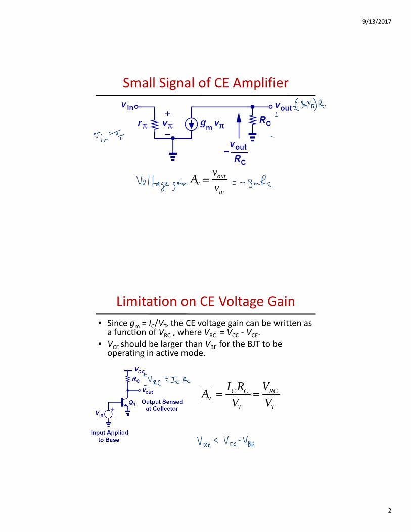
Small Signal of CE Amplifier
outv v
vA
inv
Limitation on CE Voltage Gain
• Since gm = IC/VT, the CE voltage gain can be written as a function of VRC , where VRC = VCC ‐ VCE.
• V should be larger than V for the BJT to be• VCE should be larger than VBE for the BJT to be operating in active mode.
T
RC
T
CCv V
V
V
RIA
TT VV
9/13/2017
3
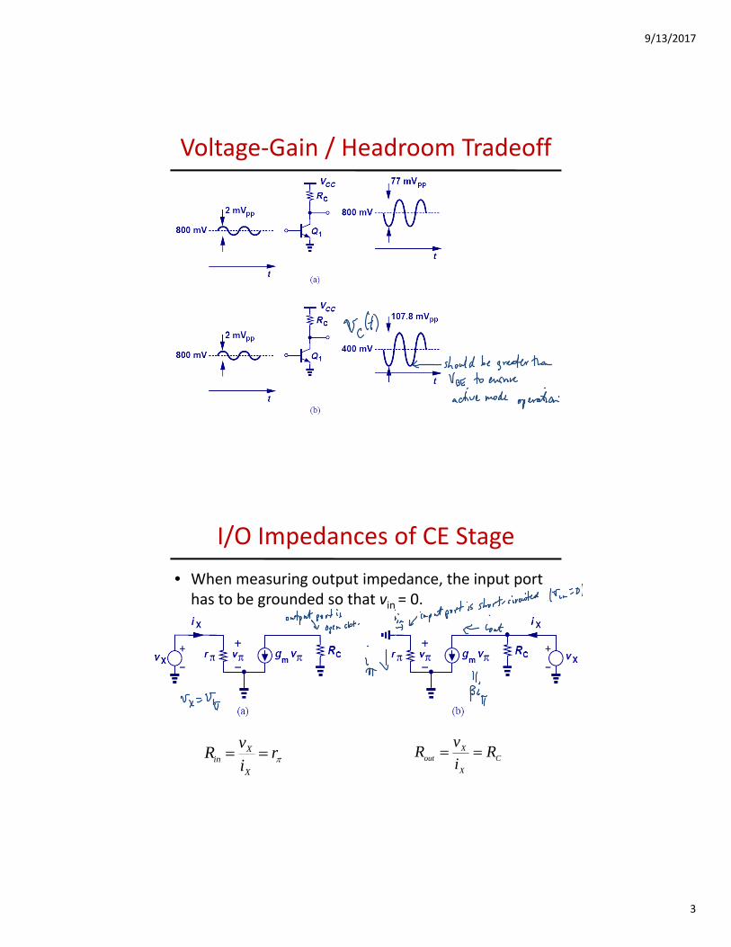
Voltage‐Gain / Headroom Tradeoff
I/O Impedances of CE Stage
• When measuring output impedance, the input port has to be grounded so that vin = 0.
riv
RX
Xin C
X
Xout R
i
vR

9/13/2017
4
CE Stage Design Trade‐offs
Inclusion of the Early Effect
• The Early effect results in reduced voltage gain of the CE amplifier.
OCout
OCmv
rRR
rRgA
||
)||(
9/13/2017
5
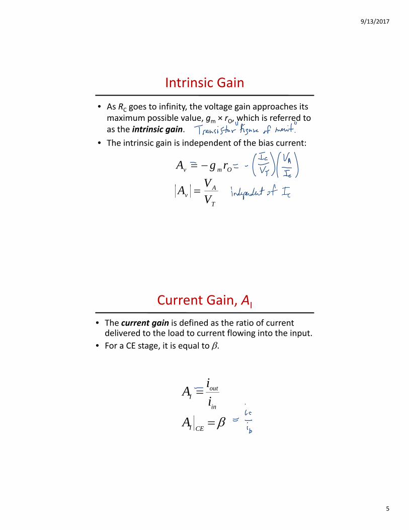
Intrinsic Gain
• As RC goes to infinity, the voltage gain approaches its maximum possible value, gm × rO, which is referred to as the intrinsic gain.
• The intrinsic gain is independent of the bias current:
A
Omv
VA
rgA
T
Av V
VA
Current Gain, AI
• The current gain is defined as the ratio of current delivered to the load to current flowing into the input.
F CE t it i l t • For a CE stage, it is equal to .
outI i
iA
CEI
in
A
i
9/13/2017
6
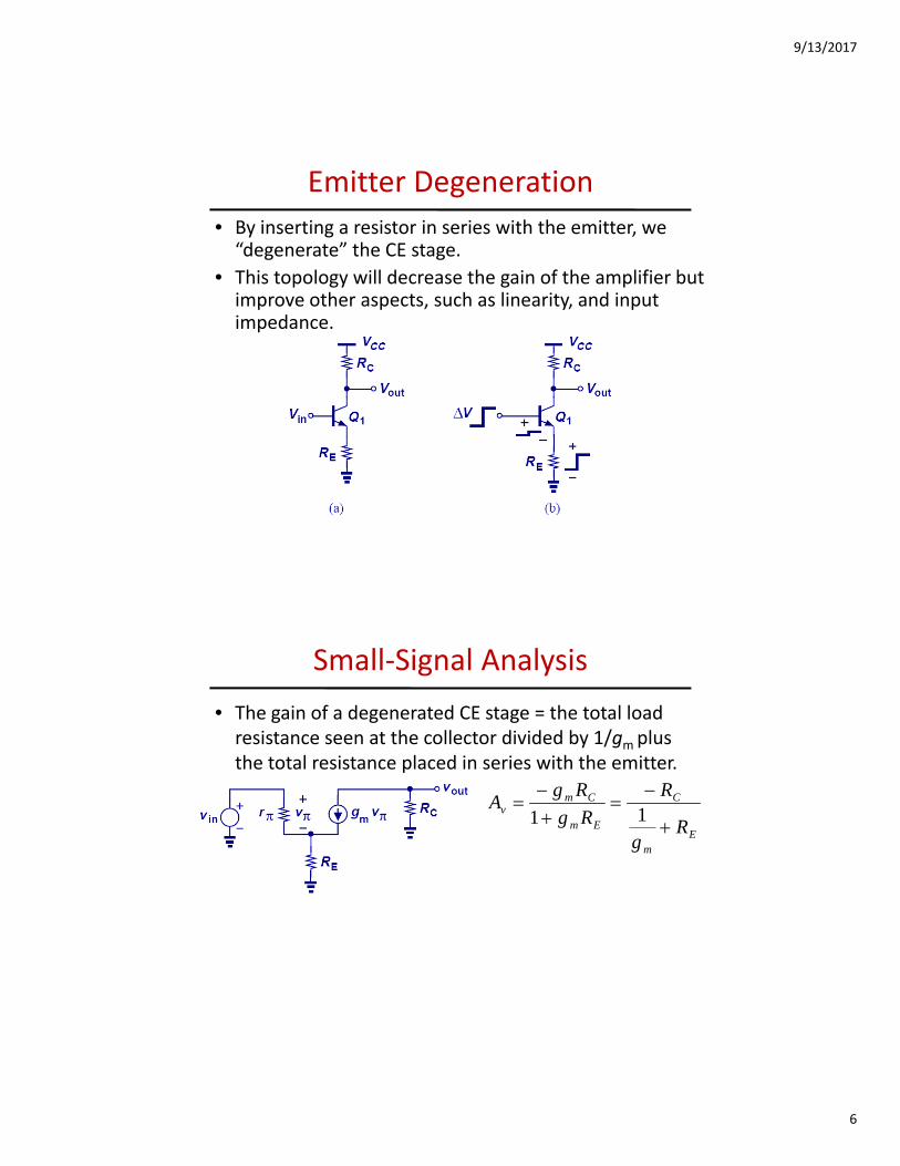
Emitter Degeneration
• By inserting a resistor in series with the emitter, we “degenerate” the CE stage.
• This topology will decrease the gain of the amplifier but• This topology will decrease the gain of the amplifier but improve other aspects, such as linearity, and input impedance.
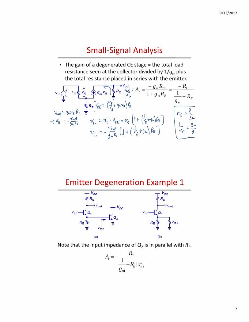
Small‐Signal Analysis
• The gain of a degenerated CE stage = the total load resistance seen at the collector divided by 1/gm plus the total resistance placed in series with the emitter.
Em
C
Em
Cmv
Rg
R
Rg
RgA
11
9/13/2017
7
Small‐Signal Analysis
• The gain of a degenerated CE stage = the total load resistance seen at the collector divided by 1/gm plus the total resistance placed in series with the emitter.
Em
C
Em
Cmv
Rg
R
Rg
RgA
11
Emitter Degeneration Example 1
Note that the input impedance of Q is in parallel with RNote that the input impedance of Q2 is in parallel with RE.
21
||1
rRg
RA
Em
Cv
9/13/2017
8
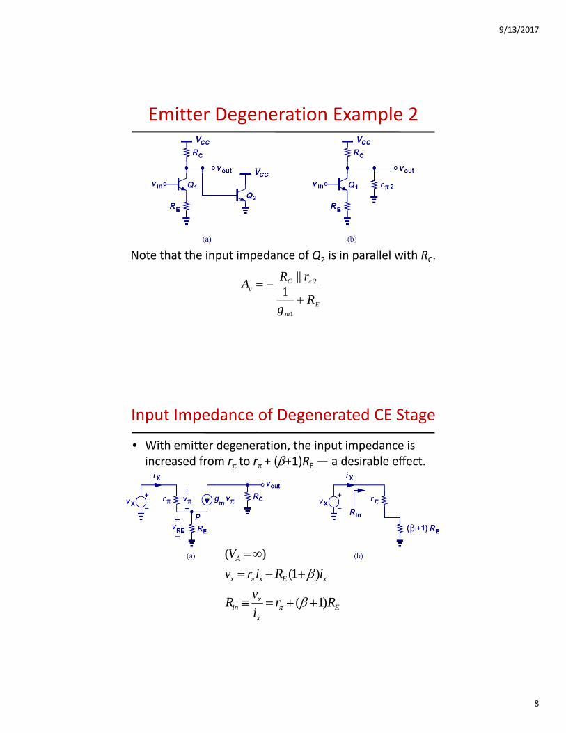
Emitter Degeneration Example 2
Note that the input impedance of Q2 is in parallel with RC.Note that the input impedance of Q2 is in parallel with RC.
E
m
Cv
Rg
rRA
1
2
1||
Input Impedance of Degenerated CE Stage
• With emitter degeneration, the input impedance is increased from r to r + (+1)RE ― a desirable effect.
AV )(
Ex
xin
xExx
A
Rri
vR
iRirv
)1(
)1(
)(
9/13/2017
9
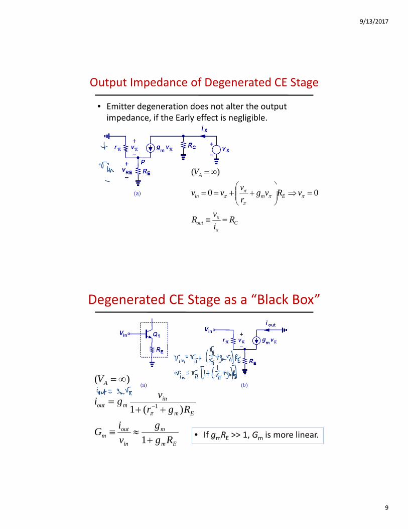
Output Impedance of Degenerated CE Stage
• Emitter degeneration does not alter the output impedance, if the Early effect is negligible.
A
v
V
)(
Cx
xout
Emin
Ri
vR
vRvgr
vvv
00
Degenerated CE Stage as a “Black Box”
in
A
vgi
V
)(
• If gmRE >> 1, Gm is more linear.Em
m
in
outm
Emmout
Rg
g
v
iG
Rgrgi
1
)(1 1

9/13/2017
10
Degenerated CE Stage with Base Resistance
)1(
.
)(
Cout
A
out
in
A
in
out
A
RRr
R
v
v
v
v
v
v
v
v
V
11
)1(
BE
m
Cv
BEin
RR
g
RA
RRrv
Degenerated CE Stage: Input/Output Impedances
• Rin1 is more important in practice, because RB is often the output impedance of the previous stage.
EBin
Ein
A
RR
RrRR
RrR
V
)1(
)1(
)(
2
1
Cout RR

9/13/2017
11
Emitter Degeneration Example
Emitter Degeneration Example
1
1)||(R
RRA C
v
1
2
2
||
)1(
11
RRR
RrR
RR
g
Cout
in
B
m
9/13/2017
12
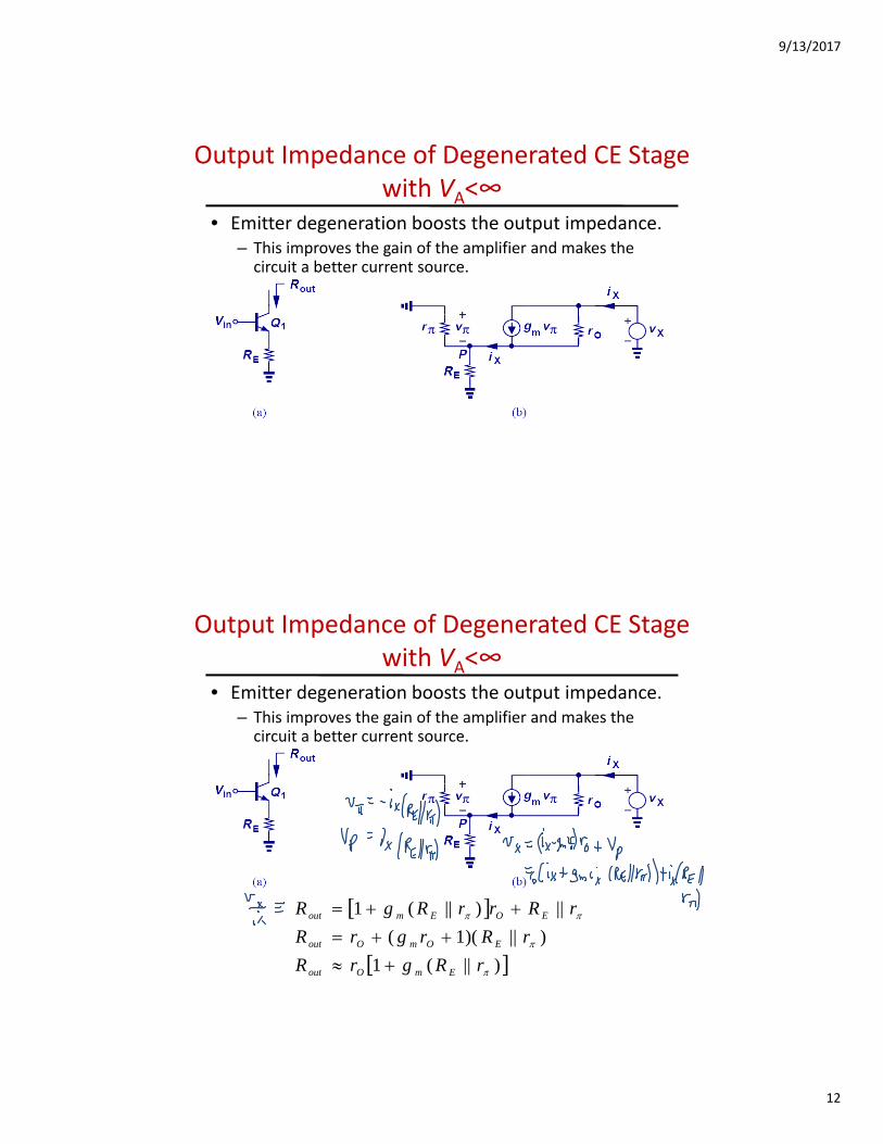
Output Impedance of Degenerated CE Stage with VA<∞
• Emitter degeneration boosts the output impedance.– This improves the gain of the amplifier and makes the circuit a better current source.circuit a better current source.
Output Impedance of Degenerated CE Stage with VA<∞
• Emitter degeneration boosts the output impedance.– This improves the gain of the amplifier and makes the circuit a better current source.circuit a better current source.
)||(1
)||)(1(
||)||(1
rRgrR
rRrgrR
rRrrRgR
EmOout
EOmOout
EOEmout
9/13/2017
13
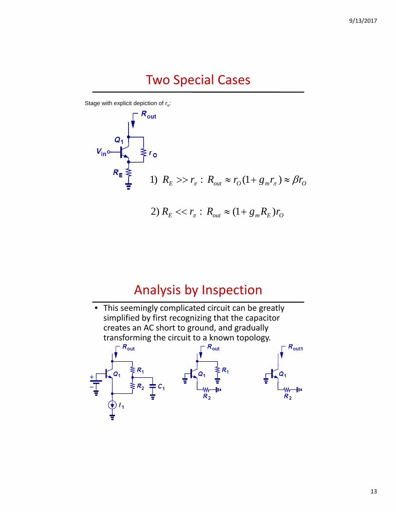
Two Special Cases
Stage with explicit depiction of ro:
rrgrRrR )1(:)1
OEmoutE
OmOoutE
rRgRrR
rrgrRrR
)1( : )2
)1( : )1
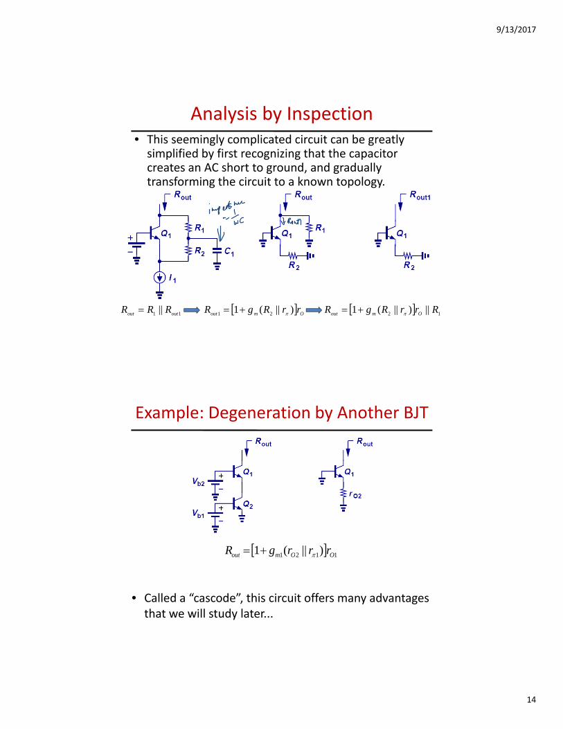
Analysis by Inspection• This seemingly complicated circuit can be greatly simplified by first recognizing that the capacitor creates an AC short to ground, and gradually g , g ytransforming the circuit to a known topology.
9/13/2017
14
Analysis by Inspection• This seemingly complicated circuit can be greatly simplified by first recognizing that the capacitor creates an AC short to ground, and gradually g , g ytransforming the circuit to a known topology.
12 ||)||(1 RrrRgR Omout Omout rrRgR )||(1 21 11 || outout RRR
Example: Degeneration by Another BJT
1121 )||(1 OOmout rrrgR
• Called a “cascode”, this circuit offers many advantages that we will study later...
1121 )||( OOmout g

9/13/2017
15
Bad Input Connection
• Since the microphone has a very low resistance (connecting the base of Q1 to ground), it attenuates the base voltage and renders Q1 with a very small bias current.
Use of Coupling Capacitor
• A capacitor is used to isolate the DC bias network from the microphone , and to short (or “couple”) the
f fmicrophone to the amplifier at higher frequencies.
9/13/2017
16
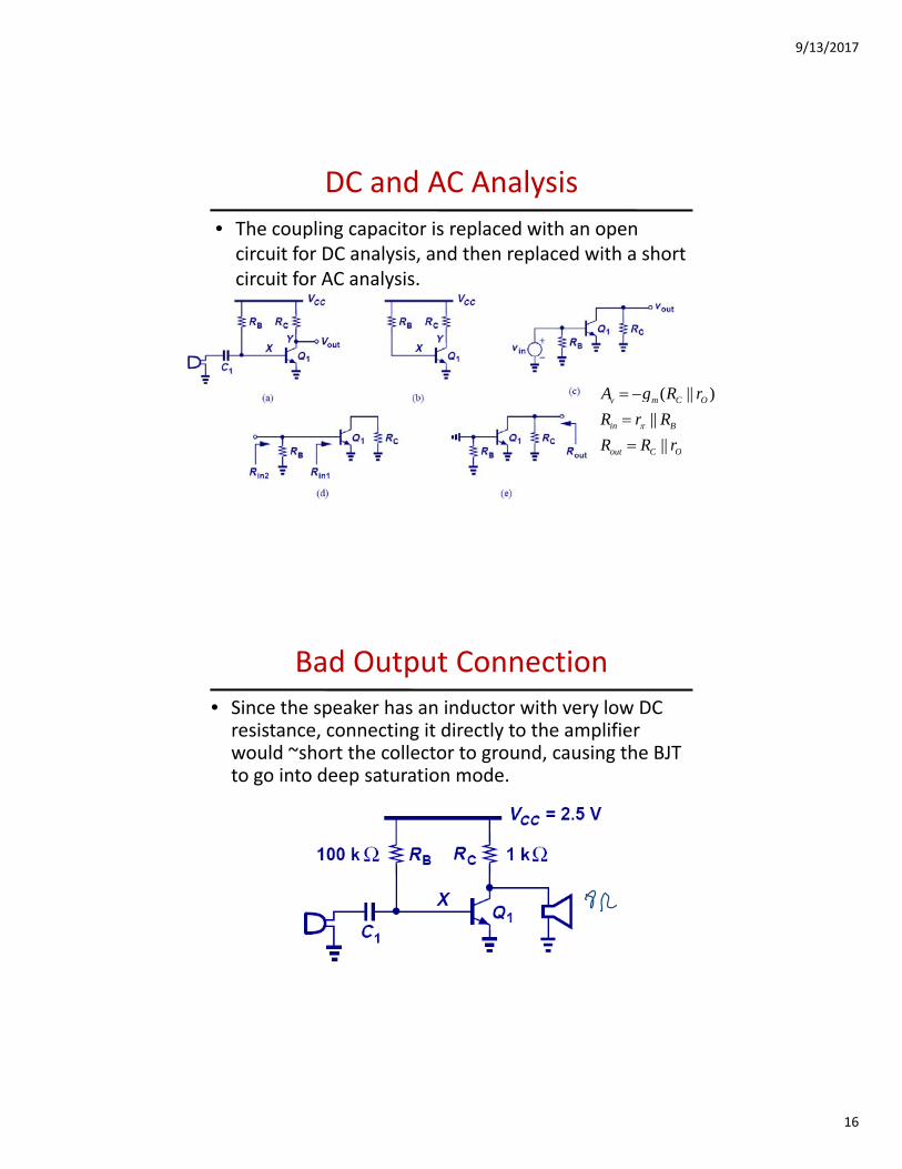
DC and AC Analysis
• The coupling capacitor is replaced with an open circuit for DC analysis, and then replaced with a short circuit for AC analysiscircuit for AC analysis.
OCmv rRgA )||(
OCout
Bin
rRR
RrR
||
||
Bad Output Connection
• Since the speaker has an inductor with very low DC resistance, connecting it directly to the amplifier would ~short the collector to ground, causing the BJTwould short the collector to ground, causing the BJT to go into deep saturation mode.
9/13/2017
17
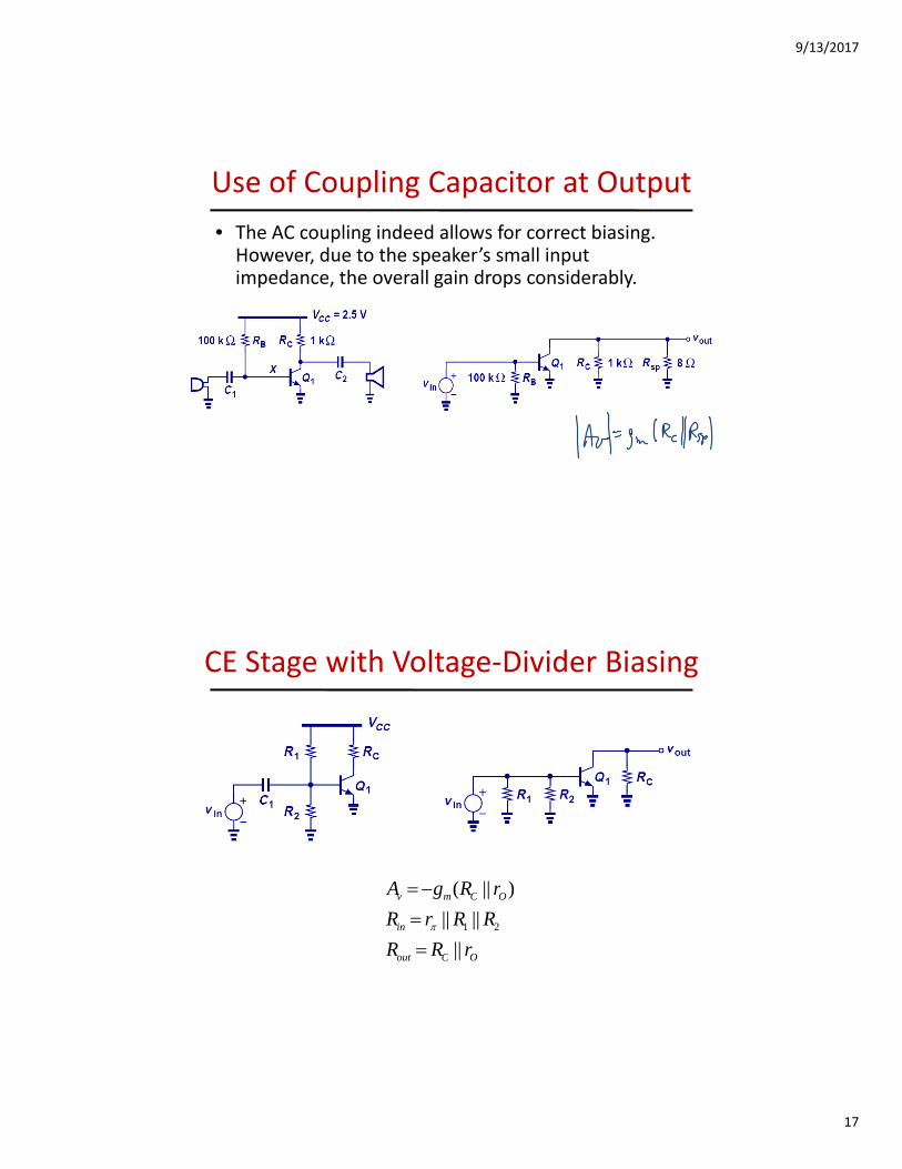
Use of Coupling Capacitor at Output
• The AC coupling indeed allows for correct biasing. However, due to the speaker’s small input impedance the overall gain drops considerablyimpedance, the overall gain drops considerably.
CE Stage with Voltage‐Divider Biasing
rRgA )||(
OCout
in
OCmv
rRR
RRrR
rRgA
||
||||
)||(
21
9/13/2017
18
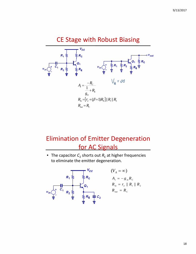
CE Stage with Robust Biasing
Cv
R
RA
1
AV
Cout
Ein
E
m
RR
RRRrR
Rg
21 ||||)1(
Elimination of Emitter Degeneration for AC Signals
• The capacitor C2 shorts out RE at higher frequencies to eliminate the emitter degeneration.
Cout
in
Cmv
RR
RRrR
RgA
21 ||||
)( AV
9/13/2017
19
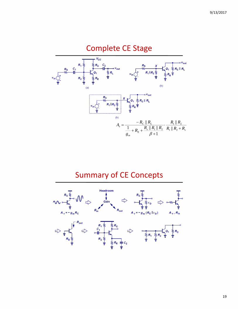
Complete CE Stage
ssE
m
LCv RRR
RRRRR
Rg
RRA
21
21
21 ||
||
1||||1
||
Summary of CE Concepts