Embed Size (px)
Citation preview

E.ON Energy Research Center Series
Commissioning of a High-Power Test Bench and Extension for HIL Testing
Nils Soltau, Hanno Stagge, Rik W. De DonckerMarija Stevic, Alexander Helmedag, Antonello Monti
Volume 6, Issue 4

E.ON Energy Research Center Series
Commissioning of a High-Power Test Bench and Extension for HIL Testing
Nils Soltau, Hanno Stagge, Rik W. De DonckerMarija Stevic, Alexander Helmedag, Antonello Monti
Volume 6, Issue 4

Contents
1 Executive Summary 1
2 Introduction 3
3 Test-Bench Hardware 53.1 Energy Supply . . . . . . . . . . . . . . . . . . . . . . . . . . . . . . . . . . . . 53.2 Test-Bench Structure and Configurations . . . . . . . . . . . . . . . . . . . . . . 5
3.2.1 General Test-Bench Structure . . . . . . . . . . . . . . . . . . . . . . . . 53.2.2 Configuration I: Inverter / Rectifier (Constant DC Voltage) . . . . . . . 83.2.3 Configuration II: Inverter / Rectifier (Variable DC Voltage) . . . . . . . 93.2.4 Configuration III: DC-DC Converter . . . . . . . . . . . . . . . . . . . . 103.2.5 Configuration IV: AC-AC Converter . . . . . . . . . . . . . . . . . . . . 113.2.6 Configuration V: Drive Test Bench . . . . . . . . . . . . . . . . . . . . . 123.2.7 Configuration VI: Medium-Frequency Transformer . . . . . . . . . . . . 133.2.8 Power Hardware-in-the-Loop . . . . . . . . . . . . . . . . . . . . . . . . 13
3.3 Power-Electronic Converters . . . . . . . . . . . . . . . . . . . . . . . . . . . . . 143.4 Mechanical Drive Train . . . . . . . . . . . . . . . . . . . . . . . . . . . . . . . 15
4 Installation and Commissioning 194.1 Water Cooling . . . . . . . . . . . . . . . . . . . . . . . . . . . . . . . . . . . . 194.2 Test-Bench Arrangement and Delivery . . . . . . . . . . . . . . . . . . . . . . . 204.3 Commissioning . . . . . . . . . . . . . . . . . . . . . . . . . . . . . . . . . . . . 20
5 Connection of Real Time Digital Simulator to Test Bench 255.1 Real-Time Digital Simulator . . . . . . . . . . . . . . . . . . . . . . . . . . . . . 255.2 RTDS analogue and digital interface cards . . . . . . . . . . . . . . . . . . . . . 275.3 Enabling closed loop testing capabilities for the Test Bench by using RTDS . . 275.4 Test Bench Hardware in the Loop interface to RTDS . . . . . . . . . . . . . . . 295.5 Testing of the HIL interface to RTDS . . . . . . . . . . . . . . . . . . . . . . . . 305.6 Impact of HIL interface on stability of closed loop testing . . . . . . . . . . . . 31
6 Conclusion 37
7 Further Steps and Future Development 38
8 Bibliography 39
9 Attachments 429.1 List of Figures . . . . . . . . . . . . . . . . . . . . . . . . . . . . . . . . . . . . 429.2 List of Tables . . . . . . . . . . . . . . . . . . . . . . . . . . . . . . . . . . . . . 439.3 Short CV of Scientists Involved in the Project . . . . . . . . . . . . . . . . . . . 439.4 Project Timeline . . . . . . . . . . . . . . . . . . . . . . . . . . . . . . . . . . . 45
i

Contents
9.5 Activities within the Scope of the Project . . . . . . . . . . . . . . . . . . . . . 46
ii

1 Executive Summary
The project “Commissioning of a high-power test bench and extension for HiL testing”, whichis kindly supported by the E.ON ERC gGmbH, has two main foci: the construction andcommissioning of a 5MW high-speed test bench and the connection of this test bench to thereal-time digital simulator (RTDS) to perform power hardware-in-the-loop (PHIL) testing.
The test bench itself is configurable and accepts a variety of test devices. Mechanical drivesup to a speed of 15 000 rpm, as well as different kinds of medium-voltage converters can betested and characterized.
In the first part of this report, the test-bench hardware is introduced. This includes themedium-voltage power supply, the power-electronic converters and the mechanical drive train.Afterwards, the different configurations of the test bench are presented and the correspondingtesting scenarios.
The following chapter describes the installation and integration of the test-bench into the testfacility of the E.ON Energy Research Center. The installation works include the design andthe construction of the water cooling and the integration of the test bench into the buildingautomation. The arrangement of the test bench within the test hall is presented as well assome impressions from the delivery of the up to 11 tons heavy components. The test bench iscommissioned under no-load conditions. This represents the worst-case scenario for the gearbox and the bearings since the damping within the drive train is minimal. The commissioninghas been performed successfully up to 15 000 rpm while all bearing temperatures have settledwithin the allowed limits.
The RTDS of the Institute for Automation of Complex Power Systems (ACS) is connectedto the test bench. RTDS is a special purpose power system simulator which performs elec-tromagnetic transient simulations in real time. The connection of RTDS to the test benchenables closed loop testing of devices for normal operation but also under various fault ornon-ideal conditions. Ultimately, the RTDS provides reference values for the controller of thetest bench inverter. Within this project, the PHIL interface between RTDS and the test benchis developed and tested.
1

Executive Summary
2

2 Introduction
Within the given project, a medium-voltage test bench is constructed and commissioned thatallows testing of different mechanical and electrical machines. Besides the flexibility of the testbench given by numerous different configurations, the high-speed testing capability of up to15 000 rpm is one of the unique features. The control hardware of the test bench is interfacedwith a real-time digital simulator (RTDS) [1], enabling power hardware-in-the-loop (PHIL)testing of equipment up to 5MW.
The test bench allows measuring of power-electronic converters and electrical drives up to5MW, of which the maximal speed is 15 000 rpm and the maximal voltage is 3.3 kV (ac) or5.5 kV (dc). The great advantage of a test bench compared to measuring in the field is thattest conditions can be fully controlled. This enhances reproducibility and comparability ofexperiments. The operation point of the device under test (DUT) can be set directly. Thus,the characterization of the entire operating range of the DUT time is achievable within shorttime.
Operating the test-bench, the energy generated by the DUT is fed back to the test bench.Consequently, the energy circulates within the test bench. This makes a high-power loadobsolete, reduces energy consumption as the grid connection only needs to supply a smallfraction of the 5MW nominal power [2].
High-speed drives are used in industry increasingly. Due to the higher speed, the volumeand mass of the drive train can be reduced. Directly coupling a 5MW gas turbine to a high-speed generator running at 15 000 rpm safes roughly 22.7 t material compared to a conventionalsystem (which applies a gearbox to couple a low-speed drive) [3, 4]. Similarly, these high-speedmachines can be used as direct turbo compressor drives, for example, in the gas industry [5,6].
Using PHIL, a device can be tested in a virtual environment. This virtual environment mightbe for example a grid with a high share of renewables. The virtual grid voltage is generatedby the test bench according to the real-time simulation of the RTDS as illustrated in Fig. 2.1.Therefore, the DUT can be tested for an infinite number of different (virtual) environmentsby adapting the models accordingly in the RTDS. Using PHIL, the DUT can be tested underextreme conditions with minimum risk.
Additionally, the DUT can be tested separately, while the other components of the drive trainare emulated by RTDS [7].
3

Introduction
Figure 2.1: principle of power hardware-in-the-loop
4

3 Test-Bench Hardware
In the following, the hardware setup of the high-speed test bench is introduced. The energysupply, the general test bench structure, the power electronic converters and the mechanicalparts are discussed.
3.1 Energy Supply
The test bench is supplied from the 10 kV grid, which is operated by the RWTH AachenUniversity. According to the varying impedance of the grid, the minimal and maximal short-circuit power at the 10 kV network connection point are [8]
Ssc,min = 69.65MVA with Isc,min = 4.02 kA (3.1)Ssc,max = 109.76MVA with Isc,max = 6.34 kA. (3.2)
Using a 2.5MVA dry-type transformer the voltage is stepped down to 3.3 kV (cf. Fig. 3.1).On the high-voltage side, the transformer windings are connected in delta configuration. Onthe low-voltage side, they are connected in star. Although the star point on the secondaryis accessible, it is not connected. The relative short-circuit voltage is 8%. The no-loadlosses are P0 = 3.6 kW and the short-circuit power at a temperature of 75 C and 120 C arePsc75 = 16.7 kW and Psc120 = 19.0 kW respectively.
The energy is fed via a vacuum circuit breaker to the test bench.
3.2 Test-Bench Structure and Configurations
3.2.1 General Test-Bench Structure
Key element of the test bench is the distributed dc link that is operated at a nominal voltageof 5 kV. The dc-link voltage is control by the converter UM 1 that serves as an active frontend (AFE). It allows bidirectional power flow, as does every other converter in the test bench.Consequently, when the test bench is slowed down, the surplus (magnetic or kinetic) energycan be fed back into the grid.
As another main feature, the energy is circulated during the operation of the test bench.Hence, the energy generated by the device under test (DUT) is not dissipated but mainly fedback to the test bench. This gives two main advantages. Firstly, the grid only needs to supplya small fraction of the testing power - namely the occurring losses. Secondly, an expensiveand bulky load and cooling systems are not required.
As depicted in Fig. 3.1, the electrical part of the test bench consists of multiple converters,labeled as UM (from the German word “Umrichter”), and several connection fields or terminals
5

Test-Bench Hardware
marked with AF (from the German word “Anschlussfeld”). Moreover, one of the converters(UM 4) is able to operate a 5MW machine. The machine is connected to a gear box withthree different output shafts. Each shaft has a different maximal output speed.
This versatility and variability of the test bench allow the measurement of different mechanical,electrical or electromechanical devices. The configuration possibilities are introduced in thefollowing.
6

Test-Bench Hardware
Figure 3.1: overview of the high-speed test bench
7

Test-Bench Hardware
3.2.2 Configuration I: Inverter / Rectifier (Constant DC Voltage)
This configuration as depicted in Fig. 3.2 allows to measure inverters or rectifiers. The DUTis connected on the ac side via a filter to UM 4. On the dc side, the DUT is connected to thedc link of the test bench.
In this configuration the DUT is operated with a fixed dc voltage. Moreover the filter has toprovide galvanic isolation. The ac voltage provided by UM 4 can be adjusted. Consequently,power hardware-in-the-loop (PHIL) and fault ride through (FRT) tests can be performed.
Figure 3.2: configuration I: inverter testing
8

Test-Bench Hardware
3.2.3 Configuration II: Inverter / Rectifier (Variable DC Voltage)
In this configuration, the dc voltage imposed to the DUT can be varied. As depicted inFig. 3.3, the dc voltage is controlled by UM 2 and UM 3 that are interconnected with amedium-frequency transformer. This topology, also referred to as dual-active bridge converter(DABC), serves as a dc-dc converter and allows to dynamically provide arbitrary dc-voltagesto the DUT [9–16]. Since the medium-frequency transformer of the DABC provides galvanicisolation, it is not required to provide isolation in the DUT filter.
Figure 3.3: configuration II: inverter testing (variable dc voltage)
9

Test-Bench Hardware
3.2.4 Configuration III: DC-DC Converter
This configuration which is shown in Fig. 3.4 allows testing dc-dc converters. The DUT isconnected to the fixed internal dc-link voltage of the test bench and to the variable dc voltagegenerated by UM 3 (cf. configuration II).
Figure 3.4: configuration III: dc-dc converter testing
10
Test-Bench Hardware
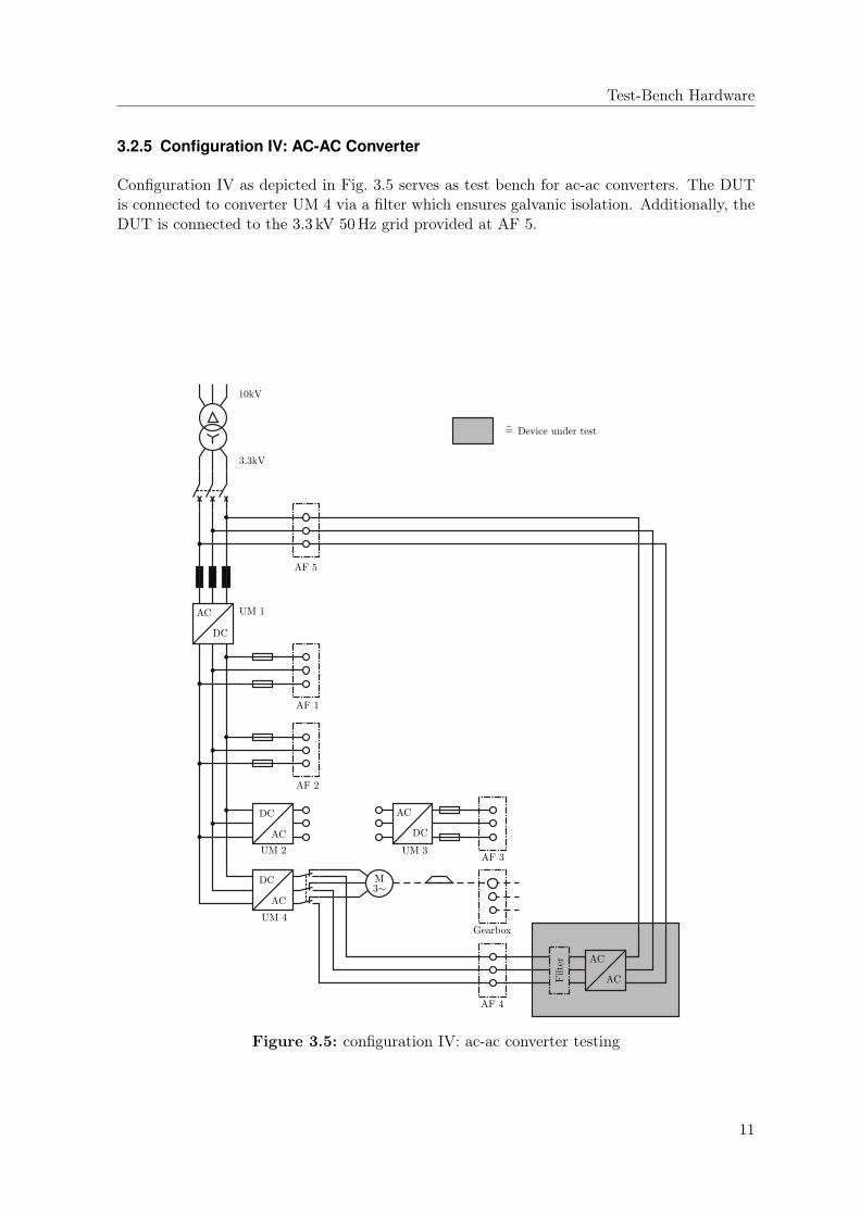
3.2.5 Configuration IV: AC-AC Converter
Configuration IV as depicted in Fig. 3.5 serves as test bench for ac-ac converters. The DUTis connected to converter UM 4 via a filter which ensures galvanic isolation. Additionally, theDUT is connected to the 3.3 kV 50Hz grid provided at AF 5.
Figure 3.5: configuration IV: ac-ac converter testing
11

Test-Bench Hardware
3.2.6 Configuration V: Drive Test Bench
Configuration V represents different electromechanical DUTs. The shaft of the machine isconnected to one of the three output shafts of the gearbox. Consequently, maximal speeds of1800 rpm, 7200 rpm and 15 000 rpm can be achieved respectively.
Depending on the drive type, the electrical output can be connected to AF 2, AF 3 or AF 5.Figure 3.6 gives the example of a DUT having an ac output, which is connected to the 3.3 kVgrid directly. The connection is equivalent to Configuration I or II if the DUT has a 5 kV dcoutput or variable dc output voltage.
Figure 3.6: configuration V: Machine Test Bench
12

Test-Bench Hardware
3.2.7 Configuration VI: Medium-Frequency Transformer
The interest in medium-frequency transformers is rising steadily. Compared to 50Hz, a1000Hz transformer offers the ten-fold power density and reduced core losses. Moreover it isa key component of high-power dc-dc converters.
Using Configuration VI as shown in Fig. 3.7 it is possible to measure these devices.
3.2.8 Power Hardware-in-the-Loop
Although it has not been stated explicitly, several of the mentioned configurations are capableof power hardware-in-the-loop simulation. The terminals AF 3, AF 4 and the mechanical
Figure 3.7: configuration VI: medium-frequency transformers
13

Test-Bench Hardware
Figure 3.8: 3-level NPC structure of the power electronic converters
drive train accept control input of real-time digital simulator (RTDS). Consequently, theseterminals can be used for power hardware-in-the-loop (PHIL) simulation and emulation.
Hence, AF 3 can act like a future meshed medium-voltage dc grid, AF 4 can emulate a special-application machine or the mechanical drive might provide arbitrary wind-field characteristics.
PHIL is introduced in more details in chapter 5.
3.3 Power-Electronic Converters
As it is common for medium-voltage drives, the power-electronic converters are 3-level neutral-point clamped (NPC) converters as depicted in Fig. 3.8. The 3-level NPC was first mentionedin 1981 [17]. It allows to set three different voltage levels at each of the three ac terminals (withrespect to M): Up, -Un and 0V. Consequently, the output voltage waveform has a lower totalharmonic distortion compared to a 2-level inverter. This results in reduced torque ripple in amachine application. Furthermore, an additional sine filter is often not necessary. Similarly,considering a grid application, the filter size can be reduced.
The converter is equipped with press-pack IGBTs and diodes. In contrast to modules, press-pack devices offer an improved heat removal due to double-side cooling. Consequently, theyare especially interesting for high-power applications. Moreover, if press-pack devices fail, theycreate a short circuit. A failure in a module might short circuit or open circuit the device.This makes the consequence of a failure hard to predict.
Since each converter is rated for a maximal output power of 10MVA, the switching frequencycan be increased compared to the typical PWM carrier frequency of 900Hz. Depending onthe power demand the switching frequency is in a range of 800Hz – 2.3 kHz.
Further information about the power-electronic converters installed by GE Energy (formerlyConverteam) can be found in [18]. A picture of the converter installed in the E.ON ERC test
14

Test-Bench Hardware
Figure 3.9: Photo of the power-electronic converters
facility is given in Fig. 3.9.
3.4 Mechanical Drive Train
The mechanical drive train contains of a motor, a gear box and an emergency brake. Thesecomponents are introduced briefly in the following.
The motor, as depicted in Fig. 3.10, is an asynchronous motor with a power rating of 5MWand a maximal speed of 1800 rpm at an electrical frequency of 50Hz. The torque is 31.8 kNmand 26.5 kNm at 1500 rpm and 1800 rpm respectively.
At the output shaft of the motor, an emergency brake is mounted, which is shown in Fig. 3.11.In normal operation, the power electronics is used to decelerate the drive train electrically.Doing so, the energy saved in the drive train is fed into the electrical grid. The mechanicalemergency brake is only used in case of a black out since recuperative braking is no longerpossible consequently. Additionally, the brake is tripped if a failure occurs that is followed byan “emergency off”. The brake is designed to reduce the speed of the drive train within 20 s to10% of the maximum speed. After a braking procedure, it is required to change the brakingpads.
As depicted in Fig. 3.12, the gear box provides three output shafts with different transmissionratios. While the first output is the same shaft as the input, the second and third output havea transmission ratio of 4.02 and 8.56 respectively. Consequently, the maximal output speedsof n1 = 1800 rpm, n2 = 7252 rpm and n3 = 15 405 rpm can be set.
Accelerating the drive train, a maximal slope of
dn1dt
= 51
mins
(3.3)
should not be exceeded. This corresponds to acceleration from 0 rpm to 1800 rpm within 6minutes.
15

Test-Bench Hardware
Figure 3.10: Photo of the 5MW motor
These timings are very high, especially when the test bench shall be shut down due to imminentdanger. The drive train might be stopped faster, if a certain mass inertia at the output is notexceeded. Assuming
Jmax,1 = 150 kgm2 at the low-speed shaft, (3.4)
Jmax,2 = 85 kgm2 at the medium-speed shaft or (3.5)
Jmax,3 = 20 kgm2 at the high-speed shaft, (3.6)
the drive train is allowed to come to a complete halt within 20 s from full speed to 0 rpm.
Due to oscillations (eigenfrequencies) in the bearings and gears, the allowed torque has to belimited in certain operating points. Figure 3.13 shows the allowed torque with respect to themaximal torque:
Tmax,1 = 31 800 kNm Tmax,2 = 7900 kNm Tmax,3 = 3700 kNm. (3.7)
The calculations depicted in Fig. 3.13 assume certain inertias at the output of the gear box.Different inertias do not influence the speeds of the limited regions. However, the maximalallowed torque in the limited operation range might vary and has to be determined for eachDUT.
16

Test-Bench Hardware
Figure 3.11: Photo of the emergency brake
Figure 3.12: Photo of a converter part (left) and the mechanical drive train (right)
17

Test-Bench Hardware
Figure 3.13: Allowed gearbox torque limits
18
4 Installation and Commissioning
4.1 Water Cooling
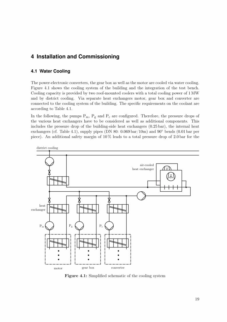
The power-electronic converters, the gear box as well as the motor are cooled via water cooling.Figure 4.1 shows the cooling system of the building and the integration of the test bench.Cooling capacity is provided by two roof-mounted coolers with a total cooling power of 1MWand by district cooling. Via separate heat exchangers motor, gear box and converter areconnected to the cooling system of the building. The specific requirements on the coolant areaccording to Table 4.1.
In the following, the pumps Pm, Pg and Pc are configured. Therefore, the pressure drops ofthe various heat exchangers have to be considered as well as additional components. Thisincludes the pressure drop of the building-side heat exchangers (0.25 bar), the internal heatexchangers (cf. Table 4.1), supply pipes (DN 80: 0.069 bar/10m) and 90 bends (0.01 bar perpiece). An additional safety margin of 10% leads to a total pressure drop of 2.0 bar for the
Figure 4.1: Simplified schematic of the cooling system
19

Installation and Commissioning
Table 4.1: Cooling-liquid requirements
water flow water flow coolant pressure drop max. inlet temp. heat loadin l/min in m3/h in bar in C in kW
motor 583.3 35 1.3 35 190gear box 280.0 16.8 0.15 30 160converter 675.0 40.5 1 30 280
motor, 0.85 bar for the gear box and 1.8 bar for the converter. Correspondent to the flow rateand the calculated pressure drop, the following pumps are installed for the different coolingcircuits:
pump model nominal power number of poles
Pm: Wilo IL 80/130-5.5/4 5.5 kW 4Pg: Wilo IL 80/170-2.2/4 2.2 kW 4Pc: Wilo IL 80/130-5.5/2 5.5 kW 2
4.2 Test-Bench Arrangement and Delivery
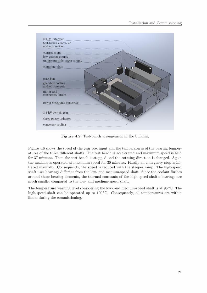
Figure 4.2 depicts the arrangement of the test-bench components within the test hall.
The biggest component is the “MV 7000”, which includes the four power-electronics converters,the dc link and the terminals. The “MV 7000” and the corresponding cooling unit are standinga few meters apart. They are interconnected with flexible tubes.
The clamping plate is located in the back of the building. On it, the motor, the brake andthe gear box are mounted. The clamping plate provides additional space for different kindsof DUTs. DUTs are brought to the clamping plate through a more than 4m wide corridorbetween the “MV7000” and the control room.
On the control room stand the test-bench controller and automation. Next to it, the inter-face to the RTDS is located. At this terminal the RTDS signals, which are send from theneighboring main building, are converted and fed into the test-bench controllers.
4.3 Commissioning
After setting up all components and when cabling was finished, the test bench was com-missioned successfully. Without a DUT it is not possible to test the test bench under loadconditions. Therefore, it was, at the writing of this report, not possible to demonstrate ratedpower.
However, the operation at no-load condition is the worst case scenario regarding the gear box.Due to the lack of a load, the damping of the shafts is low. Small oscillations of the shaftsheat up the bearing. This is also the reason, why a 200 kg cylinder had to be mounted on theslow shaft that provides a minimum damping during commissioning.
20
Installation and Commissioning
Figure 4.2: Test-bench arrangement in the building
Figure 4.6 shows the speed of the gear box input and the temperatures of the bearing temper-atures of the three different shafts. The test bench is accelerated and maximum speed is heldfor 37 minutes. Then the test bench is stopped and the rotating direction is changed. Againthe machine is operated at maximum speed for 30 minutes. Finally an emergency stop is ini-tiated manually. Consequently, the speed is reduced with the steeper ramp. The high-speedshaft uses bearings different from the low- and medium-speed shaft. Since the coolant flushesaround these bearing elements, the thermal constants of the high-speed shaft’s bearings aremuch smaller compared to the low- and medium-speed shaft.
The temperature warning level considering the low- and medium-speed shaft is at 95 C. Thehigh-speed shaft can be operated up to 100 C. Consequently, all temperatures are withinlimits during the commissioning.
21

Installation and Commissioning
Figure 4.3: One half of the power electronics converters during the delivery
Figure 4.4: Motor during the delivery
22

Installation and Commissioning
Figure 4.5: Motor, brake and gear box mounted on the clamping plate
23

Installation and Commissioning
speedin
rpm
gear-box input speed
time in minutes
temperature
in C
slow shaft
time in minutes
temperature
in C
medium shaft
time in minutes
fast shaft
time in minutes
temperature
in C
Sensor 1Sensor 2
0 10 20 30 40 50 60 70 80 90 100
0 10 20 30 40 50 60 70 80 90 100
0 10 20 30 40 50 60 70 80 90 100
0 10 20 30 40 50 60 70 80 90 100
20
40
60
80
20
40
60
80
20
40
60
80
−2000
0
2000
Figure 4.6: Bearing temperatures of the different shafts during test run
24
5 Connection of Real Time Digital Simulator to Test Bench
The Real Time Digital Simulator (RTDS) at the Institute for Automation of Complex PowerSystems (ACS) is connected to the test-bench setup in order to enable closed-loop testing capa-bilities with the device under test (DUT). RTDS realizes a simulation of the DUT environmentby means of providing reference values for the test-bench inverter. One of the tasks of theproject has been the design, the development and the construction of a hardware-in-the-loop(HIL) interface to enable the connection of RTDS with the test bench.
5.1 Real-Time Digital Simulator
The RTDS [1] is a special-purpose simulator developed for performing electromagnetic tran-sient simulations in real time. The RTDS hardware is based on a Digital Signal Processor(DSP) design in combination with a Reduced Instruction Set Computer (RISC) design. RTDSutilizes parallel processing techniques to fulfill high computational demands coming from thesimulation of power systems. The simulator is able to solve power-system equations in realtime within 50 µs, which is typical time step used for RTDS applications. Moreover, time stepdown to 2 µs can be used to provide accuracy for the simulation of faster dynamics. Suchsimulator is used by both utilities and academic research groups.
Besides its special hardware, RTDS includes two major software components designed forpower-system simulation. RSCAD Software Suite is a user-friendly software environment formodeling of power systems, running simulations and analyzing results. Furthermore, Compo-nent Model Libraries provide a significant number of already tested and validated componentsfor creating simulation models. Various power system, control system and protection compo-nents, which are integral part of RSCAD, can be used.
The RTDS system at ACS laboratory, illustrated in Fig. 5.1, consists of 8 racks with 4 processorcards (Giga Processor Card – GPC) installed in each rack. The GPC processor card, whichis specifically developed for the RTDS simulator, contains two IBM PowerPC 750GX RISCprocessors with a clock speed of 1GHz. Furthermore, a GTSYNC card (Giga-TransceiverSynchronization Card – GTSYNC) is installed, which allows the RTDS simulation time stepto be synchronized to an external time reference, for example to a GPS clock or the time stepof the DUT.
A single rack can be used for the simulation of a power system with up to 66 single-phasenodes. Therefore, the total number of 32 GPC processor cards which are available at ACS cansimulate power systems with a size of up to 528 single-phase nodes. As an advantage of themodular RTDS system, multiple racks can be used for either running simultaneous simulationsof several systems at the same time and for running large-scale power-system simulations byusing more than a single rack.
More than 20 analogue and digital input/output cards (Giga-Transceiver Input/Output – GTI/O) are connected to the GPC processor cards via fiber optic links giving the opportunity
25

Connection of Real Time Digital Simulator to Test Bench
Figure 5.1: Real-Time Digital Simulator (RTDS) at laboratory of ACS
to have both digital and analog input/output channels. The RTDS system is equipped with4 communication cards (Giga-Transceiver Network Communication Card – GTNET) whichare used for Ethernet-based communication with external equipment. The firmware of theGTNET can be configured to support different protocol options such as DNP, IEC 61850 GSEbinary messaging and IEC 61850-9-2 sampled values. In addition to the described interfacecards, two GTFPGA cards are available. The hardware of GTFPGA cards is fully based on anXilinx ML507 evaluation platform which contains a RISC processor and a “Virtex 5” FPGA.The firmware developed by RTDS supports the direct data exchange every time step between“Virtex 5” FPGA and the GPC processor card. This allows the user to develop FPGA-basedsimulation models or to implement custom communication protocols either on the FPGAor on the RISC processor. Additional flexibility comes from the option to use the availablehardware interfaces of the Xilinx ML507 platform to connect external devices via USB, RJ45,PCI Express et cetera.
Project and research work at ACS is focused on various applications that benefit from theperformance of the described RTDS system. RTDS, as advanced electromagnetic transientsimulator, is utilized to study and validate new power-system control methods [19]. Further-more, RTDS is used in the scope of various power-level HIL setups. In a previous projectthat ACS was involved in, a multi-physics power-level HIL test bench designed for the testingof wind turbine nacelles has been interfaced to RTDS to perform simulations of electricalgrids [20]. Another interesting application of RTDS implemented at ACS is the creation of atesting platform to develop advanced approaches for measurement and monitoring system foractive distribution grids [21].
26
Connection of Real Time Digital Simulator to Test Bench
5.2 RTDS analogue and digital interface cards
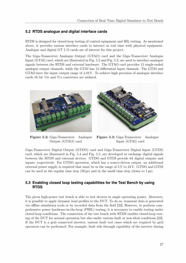
RTDS is designed for closed-loop testing of control equipment and HIL testing. As mentionedabove, it provides various interface cards to interact in real time with physical equipment.Analogue and digital GT I/O cards are of interest for this project.
The Giga-Transceiver Analogue Output (GTAO) card and the Giga-Transceiver AnalogueInput (GTAI) card, which are illustrated in Fig. 5.2 and Fig. 5.3, are used to interface analoguesignals between the RTDS and external hardware. The GTAO card provides 12 single-endedanalogue output channels, while the GTAI has 12 differential input channels. The GTAI andGTAO have the input/output range of ±10V. To achieve high precision of analogue interfacecards 16 bit A/D and D/A converters are utilized.
Figure 5.2: Giga-Transceiver AnalogueOutput (GTAO) card
Figure 5.3: Giga-Transceiver AnalogueInput (GTAI) card
Giga-Transceiver Digital Output (GTDO) card and Giga-Transceiver Digital Input (GTDI)card, which are illustrated in Fig. 5.4 and Fig. 5.5, are developed to exchange digital signalsbetween the RTDS and external devices. GTDO and GTDI provide 64 digital outputs andinputs, respectively. For GTDO operation, which has a source-driven output, an additionalexternal power supply is required that must be in the range of 5V to 24V. GTDO and GTDIcan be used in the regular time step (50 µs) and in the small time step (down to 1 µs).
5.3 Enabling closed loop testing capabilities for the Test Bench by usingRTDS
The given high-power test bench is able to test devices in single operating points. Moreover,it is possible to apply dynamic load profiles to the DUT. To do so, transient data is generatedvia offline simulation tools or by recorded data from the field [22]. However, to perform com-prehensive power hardware-in-the-loop (PHIL) testing, it is necessary to enable testing underclosed-loop conditions. The connection of the test bench with RTDS enables closed-loop test-ing of the DUT for normal operation but also under various fault or non-ideal conditions [23].If the DUT is a grid connected inverter, various fault test cases which are required by gridoperators can be performed. For example, fault ride through capability of the inverter during
27

Connection of Real Time Digital Simulator to Test Bench
Figure 5.4: Giga-Transceiver Digital Out-put (GTDO) card
Figure 5.5: Giga-Transceiver Digital In-put (GTDI) card
symmetric and asymmetric fault scenarios can be validated. Furthermore, RTDS can simu-late the rest of the system to which the DUT is connected to, such as an electrical grid. Thisprovides additional functionalities to the test bench. It is possible, for example, to evaluatethe impact of inverters on the electrical grid and to study potential perturbations.
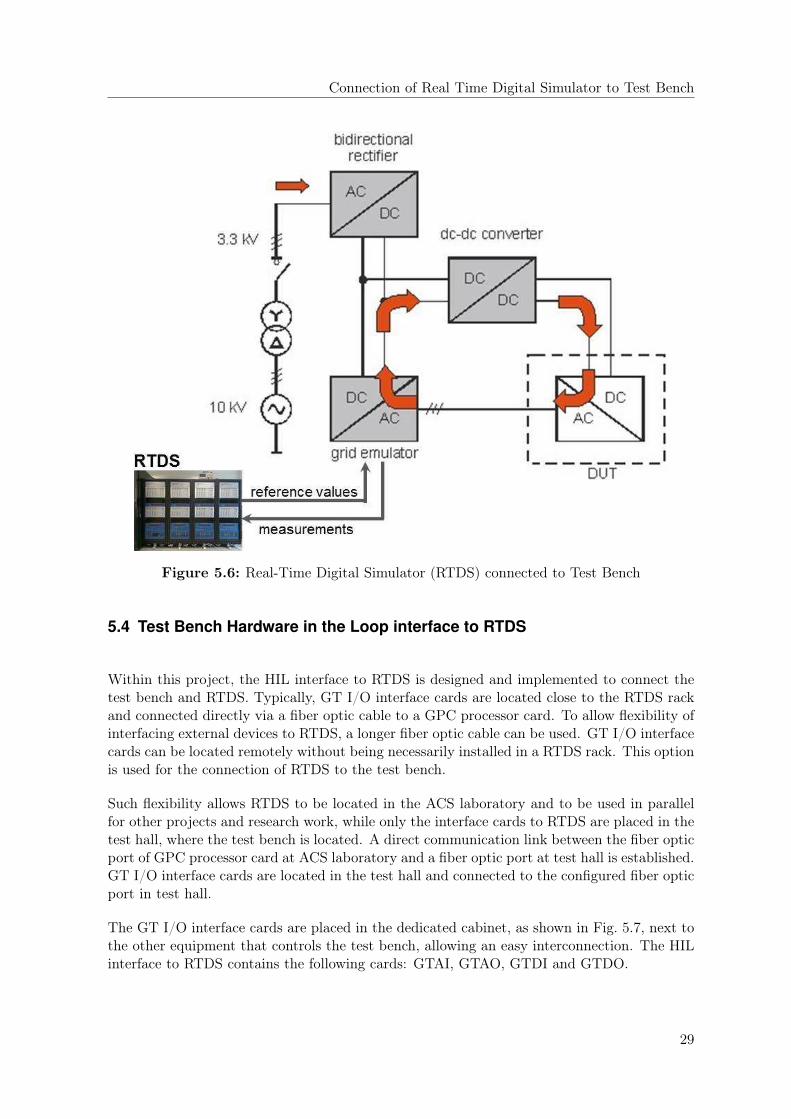
RTDS provides the output reference values for the controller of the test-bench inverter, asillustrated in Fig. 5.6, while measurements are fed back into RTDS in order to interface theDUT to the simulation model.
To provide the described data exchange between RTDS and the controller of the test-benchinverter, a signal-level HIL interface is implemented as described in 5.4. The HIL interface toRTDS is developed by means of analogue signals.
PHIL refers to the testing when a real power device is interfaced to real-time simulator whichsimulates the rest of the system [24]. The major challenge is to develop the interface betweenthe simulator and the real power device which is the DUT [25]. The DUT operates at significantpower levels while the interface between the test bench and the real-time simulator runs atsignal level only. Furthermore, by processing the signal level I/O, the simulation-to-hardwareinterface must enforce conservation of energy at the point of common coupling (PCC).
The test bench is capable of testing various power devices, as defined by the test-bench config-urations (cf. chapter 3.2). To describe the concept of PHIL testing, a grid connected inverteris assumed as DUT. The real source of power for the DUT is provided by the test-benchinverter, configured as a controlled voltage source. To ensure conservation of energy at PCC,the inverter is controlled to track the voltage reference, which is obtained from RTDS. On theother side, values of current measured at PCC are sent back to RTDS and fed into the real-timemodel. In the described example the test bench inverter is in service as grid emulator. RTDSsimulates electrical grid to which the DUT is connected to. Conservation of energy must bealso enforced on the simulation side. It should be underlined that such a scenario is muchcloser to reality than the applications of grid emulators based on pre-calculated waveforms.In the PHIL scenario, effects such as unexpected reactions of the DUT can be fed back to thereal-time model and its consequences can be evaluated.
28
Connection of Real Time Digital Simulator to Test Bench
Figure 5.6: Real-Time Digital Simulator (RTDS) connected to Test Bench
5.4 Test Bench Hardware in the Loop interface to RTDS
Within this project, the HIL interface to RTDS is designed and implemented to connect thetest bench and RTDS. Typically, GT I/O interface cards are located close to the RTDS rackand connected directly via a fiber optic cable to a GPC processor card. To allow flexibility ofinterfacing external devices to RTDS, a longer fiber optic cable can be used. GT I/O interfacecards can be located remotely without being necessarily installed in a RTDS rack. This optionis used for the connection of RTDS to the test bench.
Such flexibility allows RTDS to be located in the ACS laboratory and to be used in parallelfor other projects and research work, while only the interface cards to RTDS are placed in thetest hall, where the test bench is located. A direct communication link between the fiber opticport of GPC processor card at ACS laboratory and a fiber optic port at test hall is established.GT I/O interface cards are located in the test hall and connected to the configured fiber opticport in test hall.
The GT I/O interface cards are placed in the dedicated cabinet, as shown in Fig. 5.7, next tothe other equipment that controls the test bench, allowing an easy interconnection. The HILinterface to RTDS contains the following cards: GTAI, GTAO, GTDI and GTDO.
29

Connection of Real Time Digital Simulator to Test Bench
Figure 5.7: Hardware in the Loop interface to RTDS
5.5 Testing of the HIL interface to RTDS
A fiber optic cable creates the link between RTDS and the test hall. Such an interface aswell as D/A and A/D converters of the interface themselves affect the performance of the dataexchange between RTDS and the test bench. Simple tests are performed in order to verify thebasic functionality of the HIL interface to RTDS and to evaluate its transparency with regardto the test bench.
At first, the communication loop is closed by means of GTAO and GTAI cards in order totest the latency of the connection between the test bench and RTDS which is located in theACS laboratory. A sine wave of 50Hz is generated in RTDS and sent to the GTAO channel,which is directly wired to the GTAI channel. Figure 5.8 illustrates the sine wave observed atthe input channel of GTAI as obtained by the RTDS rack in the ACS laboratory.
Test results show that latency is around 30 µs, which is less than a single time step used byRTDS. The measured time includes the time for sending signal from RTDS located at ACSlaboratory to GTAO card located at test hall over fiber optic link, D/A and A/D conversion ofGTAO and GTAI cards as well as the time for sending signal back from test hall to RTDS overfiber optic link. Therefore, the time required to send signal from RTDS to test bench hardwareis around 15 µs. This means that the impact of the HIL interface to RTDS can be neglectedcompared to the dynamics of test-bench inverter, which is in the range of milliseconds. It can
30

Connection of Real Time Digital Simulator to Test Bench
Figure 5.8: Generated and observed sine wave
be concluded that the HIL interface to RTDS is transparent with regard to the dynamics ofthe test bench.
5.6 Impact of HIL interface on stability of closed loop testing
As described, RTDS is connected to the test bench to provide reference values for the controllerof the test bench inverter. The test-bench inverter acts as a real source of power for DUT, whileRTDS simulates the rest of the system (ROS). It is not possible to design an ideal interfacebetween the DUT and the simulated ROS, which is represented in RTDS. Limitations areexist due to the communication and processing delays, sampling rates of sensors and A/Dconverters as well as due to the limited dynamic range of the test-bench inverter itself andthe performance of its controller. These limitations and imperfections may affect the stabilityand the accuracy of the platform for PHIL testing [26].
A simple test case is selected to present the PHIL concept and the mutal impact of interfacingDUT and simulated ROS regarding the stability of the overall system [27]. In the followinganalysis, considered parameters are communication delay of the HIL interface to RTDS, pro-cessing delay and sampling period of measurements. A comprehensive study should includedynamics and parameters of the test-bench inverter as well. It is assumed that the DUT is anRL load, with parameters R2 and L2, supplied by the ROS. The ROS is a simple AC sourcewith an internal resistance R1. The integrated system is shown in the Fig. 5.9.
Figure 5.10 illustrates the basic concept of PHIL testing and interfacing the DUT to the ROS
31

Connection of Real Time Digital Simulator to Test Bench
Figure 5.9: Integrated system
simulated in RTDS. In the RTDS model of the ROS, the simulation interface to the DUTis described by means of a current source that is controlled by current measurements at theDUT itself. It is assumed that the current sensor is an ideal sampler with a sampling periodh = 50 µs, which is equal to the standard time step used in RTDS. The test bench inverter isrepresented as an ideal voltage source that is directly controlled by a voltage reference obtainedfrom the simulated ROS in RTDS. Since the simulated ROS is a discrete-time system, theZero-Order Hold (ZOH) block represents the conversion of a discrete-time signal to a sequenceof rectangular pulses. The time delay block introduced before the ZOH block represents thesum of communication and processing delays.
The ROS and DUT, together with the ideal controlled voltage source, which represents thetest-bench inverter, are simulated in RTDS. However, they are separated into two subsystems.Subsystem 1 includes the ROS, while subsystem 2 entails the DUT and the ideal voltage sourcerealized through the PHIL interface. Subsystem 1 and subsystem 2 exchange instantaneousvoltage and current values by means of the test-bench HIL interface to RTDS located in thetest hall and not directly within the simulator.
At first, the time delay τ is evaluated. This delay represents the time necessary to generate thevoltage reference in subsystem 1, the communication delay between the subsystems and thetime to establish the appropriate value at the voltage source that supplies DUT in subsystem2. The evaluated delay is τ = 170 µs, which is shown in Fig. 5.11.
Such a simple example allows an analytical analysis of the system dynamics and stabilityevaluation. With reference to the Fig. 5.10, dynamics of the DUT can be expressed by thefollowing differential equation:
di(t)
dt= ai(t) + bv(t− τ) (5.1)
where a = −R2/L2 and b = 1/L2. A discrete-time model of the ROS is defined by:
vk = −R1ik + ek (5.2)
32
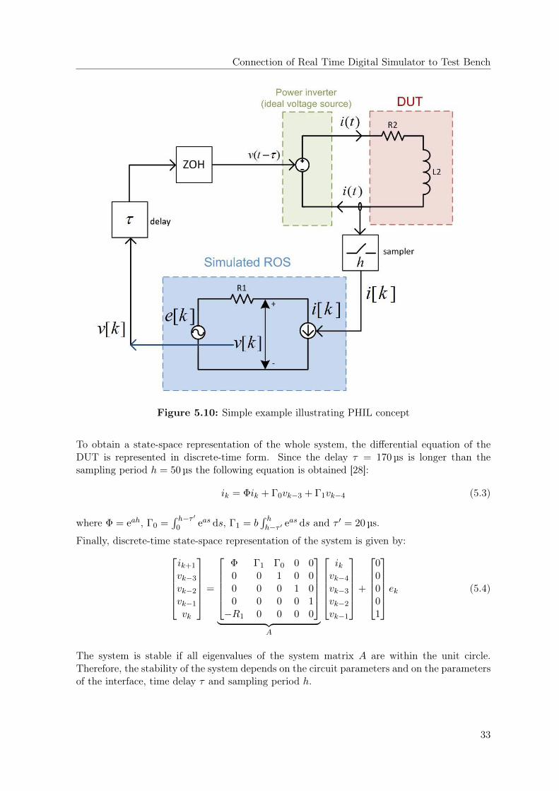
Connection of Real Time Digital Simulator to Test Bench
Figure 5.10: Simple example illustrating PHIL concept
To obtain a state-space representation of the whole system, the differential equation of theDUT is represented in discrete-time form. Since the delay τ = 170 µs is longer than thesampling period h = 50 µs the following equation is obtained [28]:
ik = Φik + Γ0vk−3 + Γ1vk−4 (5.3)
where Φ = eah, Γ0 =∫ h−τ ′0 eas ds, Γ1 = b
∫ hh−τ ′ eas ds and τ ′ = 20 µs.
Finally, discrete-time state-space representation of the system is given by:ik+1
vk−3vk−2vk−1vk
=
Φ Γ1 Γ0 0 00 0 1 0 00 0 0 1 00 0 0 0 1
−R1 0 0 0 0
︸ ︷︷ ︸
A
ikvk−4vk−3vk−2vk−1
+
00001
ek (5.4)
The system is stable if all eigenvalues of the system matrix A are within the unit circle.Therefore, the stability of the system depends on the circuit parameters and on the parametersof the interface, time delay τ and sampling period h.
33

Connection of Real Time Digital Simulator to Test Bench
Figure 5.11: Evaluation of time delay between two subsystems that exchange values bymeans of test bench HIL interface to RTDS located in the test hall
Figure 5.12 illustrates the location of the eigenvalues of the system matrix for τ = 170 µs, h =50 µs, R1 = 3 Ω and R2 = 1 Ω, while parameter L2 varies from L2 = 0.1mH to L2 = 20mH.A stable operating region is obtained for L2 > 0.28mH.
Analytical analysis on the stability can be validated by a simulation in RTDS. As mentioned,the ROS and DUT are simulated in RTDS as separated subsystems that exchange voltagereference value and current measurement by means of the HIL interface located in the testhall. Figure 5.13 (a) and (b) show the current at the DUT for L2 = 10mH and L2 = 0.2mH,respectively, as well as the location of eigenvalues of the system matrix.
The depicted simulation results verify the conclusions regarding the stability of the systembased on an analytical approach. Interfacing DUT and the simulated ROS can make theoverall system unstable, with the stability depending on the parameters of the DUT, as wellas the simulated ROS and the interface itself. However, an analytical approach is feasible onlyfor simple power systems. A simulation-based approach is suggested for stability evaluationof more complicated power systems.
34

Connection of Real Time Digital Simulator to Test Bench
Figure 5.12: Location of the system eigenvalues for L2 = 0.1mH to L2 = 20mH
35

Connection of Real Time Digital Simulator to Test Bench
(a) L2 = 10mH
(b) L2 = 0.2mH
Figure 5.13: Simulation results in the time domain
36

6 Conclusion
A 5MW high-speed test bench has been successfully constructed and commissioned underno-load conditions. The test-bench allows testing mechanical drives up to 15 000 rpm andpower-electronic converters at medium-voltage levels.
Firstly, the test hall of the E.ON Energy Research Center has been prepared. The preparationincludes adaption of the cooling water supply, modification of the medium-voltage feeder, thelow-voltage auxiliary supply and the integration of the test-bench control into the building au-tomation. Subsequent to the delivery of the test-bench components, where a single componentweighs up to 11 tons, the test bench has been arranged in the test hall. After wiring the powerelectronic converters, motor, gearbox, ac filters, test-bench controller and low-voltage auxil-iaries, the test bench has been commissioned successfully. During the no-load test, which isthe worst-case scenario for the high-speed bearings, the test bench has been operated withoutany abnormalities and all bearing temperatures have settled within the allowed limits.
The connection the real-time digital simulator (RTDS), which is located in the E.ON ERCMain Building next-door, has been setup successfully. The transfer delay of the optical linkincluding the digital-analog converters is around 15 µs. Consequently, the latency of theconnection is sufficiently fast and does not affect the real-time simulation the considered timeconstants.
37

7 Further Steps and Future Development
Since the test bench is commissioned and ready for use, the E.ON Energy Research Centerhas now the possibility to operate, test and assess performance of high-speed machines andmedium-voltage converters. The ability to operate and measure a variety of high-power com-ponents in a single test bench is unique, especially for a university. Besides measuring, thetest-bench enables to develop and improve medium-voltage converters, drives and their controlalgorithms.
Especially interesting are research topics that are very promising for future energy supply sys-tems, but have been disregarded by industry for various reasons. These research topics includehigh-power medium-voltage dc-dc converters or switched reluctance machines for mega-wattapplications. Such projects may be conducted in the future. Besides the evaluation of newdevelopments, the test bench also enables to improve existing components and their control,together with industry.
One of the challenges of interfacing a real power device to a simulated system is stability andaccuracy of closed loop testing. Stability and accuracy are affected by communication andprocessing delays, limited dynamic range of the test bench inverter itself and performance of itscontroller. Within the scope of this project, an analytical analysis of stability issue is performedbased on a simple example. Future research should focus on more comprehensive analyses ofstability and accuracy that include inherent limitations of the testing facility. Furthermore,advanced interface algorithms should be studied and developed based on stability and accuracyanalyses.
38

8 Bibliography
[1] RTDS Technologies Inc., The world standard for real time digital power system simula-tion, Homepage, [Accessed 2014-06-30], 2014. [Online]. Available: http://www.rtds.com.
[2] A. Wallace, A. Von Jouanne, and T. Rollman, “A fully regenerative, high power testingfacility for motors, drives and generators”, in IEEE Int. Electric Machines and DrivesConf. Record, 1997, MB2/13.1–MB2/13.3. doi: 10.1109/IEMDC.1997.604143.
[3] K. Pesyna, R. Hebner, A. Ouroua, et al., “High speed generator options for direct cou-pled gas turbine flight and ground based power systems”, in 8. Annual Directed EnergyProfessionals Society Symposium, Hawaii, USA, 2005.
[4] S. Z. Vijlee, A. Ouroua, L. Domaschk, and J. Beno, “Directly-coupled gas turbine per-manent magnet generator sets for prime power generation on board electric ships”,in IEEE Electric Ship Technologies Symposium (ESTS ’07), 2007, pp. 340–347. doi:10.1109/ESTS.2007.372108.
[5] H. Walter, A. Moehle, and M. Bade, “Asynchronous solid rotors as high-speed drives inthe megawatt range”, in IEEE Petroleum and Chemical Industry Technical Conf (PCIC’07), 2007, pp. 1–8. doi: 10.1109/PCICON.2007.4365799.
[6] P. Kollensperger, C. Meyer, U. Schwarzer, et al., “High-power converter systems forhigh-speed generators”, in European Conf. on Power Electronics and Applications, 2005,9 pp.–P.9. doi: 10.1109/EPE.2005.219756.
[7] M. Steurer, C. Edrington, M. Sloderbeck, et al., “A megawatt-scale power hardware-in-the-loop simulation setup for motor drives”, IEEE Transactions on Industrial Electronics,vol. 57, no. 4, pp. 1254–1260, 2010, issn: 0278-0046. doi: 10.1109/TIE.2009.2036639.
[8] S. Scherret, Kurschlussstroeme /-leistungen an e.on versuchshalle, Personal E-Mail, Apr.15, 2010.
[9] R. De Doncker, D. Divan, and M. Kheraluwala, “A three-phase soft-switched high-power-density dc/dc converter for high-power applications”, Industry Applications, IEEETransactions on, vol. 27, no. 1, pp. 63 –73, 1991, issn: 0093-9994. doi: 10.1109/28.67533.
[10] R. U. Lenke, “A contribution to the design of isolated dc-dc converters for utility appli-cations”, PhD thesis, RWTH Aachen, 2012.
[11] S. P. Engel, N. Soltau, H. Stagge, and R. W. De Doncker, “Dynamic and balanced controlof three-phase high-power dual-active bridge dc-dc converters in dc-grid applications”,Power Electronics, IEEE Transactions on, vol. 28, no. 4, pp. 1880–1889, 2013, issn:0885-8993. doi: 10.1109/TPEL.2012.2209461.
[12] S. Engel, N. Soltau, H. Stagge, and R. De Doncker, “Improved instantaneous currentcontrol for high-power three-phase dual-active bridge dc-dc converters”, Power Elec-tronics, IEEE Transactions on, vol. PP, no. 99, pp. 1–1, 2013, issn: 0885-8993. doi:10.1109/TPEL.2013.2283868.
39

Bibliography
[13] N. Soltau, S. Engel, H. Stagge, and R. De Doncker, “Compensation of asymmetric trans-formers in high-power dc-dc converters”, in ECCE Asia Downunder (ECCE Asia), 2013IEEE, 2013, pp. 1084–1090. doi: 10.1109/ECCE-Asia.2013.6579243.
[14] N. Soltau, D. Eggers, K. Hameyer, and R. W. D. Doncker, “Iron losses in a medium-frequency transformer operated in a high-power dc-dc converter”, IEEE Transaction onMagnetics, vol. 50, no. 2, 2013.
[15] N. Soltau, J. Lange, H. Stagge, and R. W. D. Doncker, “Ensuring soft-switching oper-ation of a three-phase dual-active bridge dc-dc converter applying an auxiliary resonant-commutated pole”, in European Conference on Power Electronics and Applications (EPE),[submitted for publication], 2014.
[16] N. Soltau, O. Apeldoorn, H. Stagge, and R. W. De Doncker, “Development and demon-stration of a medium-voltage high-power dc-dc converter for dc distribution systems”,in Proc. of the 5th Int. Symposium on Power Electronics for Distributed GenerationSystems (PEDG), Galway, Ireland, 2014.
[17] A. Nabae, I. Takahashi, and H. Akagi, “A new neutral-point-clamped pwm inverter”,Industry Applications, IEEE Transactions on, vol. IA-17, no. 5, pp. 518–523, 1981, issn:0093-9994. doi: 10.1109/TIA.1981.4503992.
[18] Converteam, MV7000, Brochure, [Accessed 2014-06-04], 2007. [Online]. Available: http://www.proloc.com.pl/img/Pdf/napedy/MV7000.pdf.
[19] J. Tang, J. Liu, F. Ponci, and A. Monti, “Adaptive load shedding based on combinedfrequency and voltage stability assessment using synchrophasor measurements”, PowerSystems, IEEE Transactions on, 2013.
[20] A. Helmedag, T. Isermann, A. Monti, et al., “Multi-physics power hardware in the looptest bench for on-shore wind turbine nacelles”, in ECCE Asia Downunder (ECCE Asia),2013 IEEE.
[21] J. Liu, “Measurement system and technique for future active distribution grids”, PhDthesis, Fac. for Elect. Eng., RWTH Aachen Univ., Germany, 2013.
[22] J. Mahseredjian, V. Dinavahi, and J. A. Martinez, “Simulation tools for electromagnetictransients in power systems: overview and challenges”, Power Delivery, IEEE Transac-tions on, 2009.
[23] A. Helmedag, T. Isermann, and A. Monti, “Fault ride through certification of windturbines based on a hardware in the loop setup”, Instrumentation and Measurement,IEEE Transactions on, 2014.
[24] S. Goyal, G. Ledwich, and A. Ghosh, “Power network in loop: a paradigm for real-timesimulation and hardware testing”, Power Delivery, IEEE Transactions on, 2010.
[25] S. Lentijo, S. D Arco, and A. Monti, “Comparing the dynamic performances of powerhardware-in-the-loop interfaces”, Industrial Electronics, IEEE Transactions on, 2010.
[26] W. Ren, M. Steurer, and T. Baldwin, “Improve the stability and the accuracy of powerhardware-in-the-loop simulation by selecting appropriate interface algorithms”, IndustryApplications, IEEE Transactions on, 2008.
[27] S. Ayasun, A. Monti, R. Dougal, et al., “On the stability of hardware in the loop simu-lation”, in International Conference on Modeling and Simulation of Electric Machines,Converters and Systems (ELECTRIMACS 2002).
40

Bibliography
[28] W. Zhang, M. Branicky, and S. Phillips, “Stability of networked control systems”, ControlSystems, IEEE, 2001.
41

9 Attachments
9.1 List of Figures
2.1 principle of power hardware-in-the-loop . . . . . . . . . . . . . . . . . . . . . . . 4
3.1 overview of the high-speed test bench . . . . . . . . . . . . . . . . . . . . . . . . 7
3.2 configuration I: inverter testing . . . . . . . . . . . . . . . . . . . . . . . . . . . 8
3.3 configuration II: inverter testing (variable dc voltage) . . . . . . . . . . . . . . . 9
3.4 configuration III: dc-dc converter testing . . . . . . . . . . . . . . . . . . . . . . 10
3.5 configuration IV: ac-ac converter testing . . . . . . . . . . . . . . . . . . . . . . 11
3.6 configuration V: Machine Test Bench . . . . . . . . . . . . . . . . . . . . . . . . 12
3.7 configuration VI: medium-frequency transformers . . . . . . . . . . . . . . . . . 13
3.8 3-level NPC structure of the power electronic converters . . . . . . . . . . . . . 14
3.9 Photo of the power-electronic converters . . . . . . . . . . . . . . . . . . . . . . 15
3.10 Photo of the 5MW motor . . . . . . . . . . . . . . . . . . . . . . . . . . . . . . 16
3.11 Photo of the emergency brake . . . . . . . . . . . . . . . . . . . . . . . . . . . . 17
3.12 Photo of a converter part (left) and the mechanical drive train (right) . . . . . 17
3.13 3-level NPC structure of the power electronic converters . . . . . . . . . . . . . 18
4.1 Simplified schematic of the cooling system . . . . . . . . . . . . . . . . . . . . . 19
4.2 Test-bench arrangement in the building . . . . . . . . . . . . . . . . . . . . . . 21
4.3 One half of the power electronics converters during the delivery . . . . . . . . . 22
4.4 Motor during the delivery . . . . . . . . . . . . . . . . . . . . . . . . . . . . . . 22
4.5 Motor, brake and gear box mounted on the clamping plate . . . . . . . . . . . . 23
4.6 Bearing temperatures of the different shafts during test run . . . . . . . . . . . 24
5.1 Real-Time Digital Simulator (RTDS) at laboratory of ACS . . . . . . . . . . . . 26
5.2 Giga-Transceiver Analogue Output (GTAO) card . . . . . . . . . . . . . . . . . 27
5.3 Giga-Transceiver Analogue Input (GTAI) card . . . . . . . . . . . . . . . . . . 27
5.4 Giga-Transceiver Digital Output (GTDO) card . . . . . . . . . . . . . . . . . . 28
5.5 Giga-Transceiver Digital Input (GTDI) card . . . . . . . . . . . . . . . . . . . . 28
42
Attachments
5.6 Real-Time Digital Simulator (RTDS) connected to Test Bench . . . . . . . . . . 29
5.7 Hardware in the Loop interface to RTDS . . . . . . . . . . . . . . . . . . . . . . 30
5.8 Generated and observed sine wave . . . . . . . . . . . . . . . . . . . . . . . . . 31
5.9 Integrated system . . . . . . . . . . . . . . . . . . . . . . . . . . . . . . . . . . . 32
5.10 Simple example illustrating PHIL concept . . . . . . . . . . . . . . . . . . . . . 33
5.11 Evaluation of time delay between two subsystems that exchange values bymeans of test bench HIL interface to RTDS located in the test hall . . . . . . . 34
5.12 Location of the system eigenvalues for L2 = 0.1mH to L2 = 20mH . . . . . . . 35
5.13 Simulation results in the time domain . . . . . . . . . . . . . . . . . . . . . . . 36
9.2 List of Tables
4.1 Cooling-liquid requirements . . . . . . . . . . . . . . . . . . . . . . . . . . . . . 20
9.3 Short CV of Scientists Involved in the Project
Dipl.-Ing. Nils Soltau
• 2010: Received Dipl.-Ing. degree in Electrical Engineering and Information Technology,at RWTH Aachen University, Germany
• Since 2010: Research Associate at the Institute for Power Generation and Storage Sys-tems (PGS) of the E.ON Energy Research Center of RWTH Aachen University, Germany
Dr.-Ing. Hanno Stagge
• 2004: Graduated in Power-System Engineering at Technical University Clausthal, Ger-many
• 2004 - 2010: Research Associate at the “Institut fuer Elektrische Energietechnik” ofTechnical University Clausthal, Germany
• 2010: Doctor in Power-System Engineering at Technical University Clausthal, Germany
• Since 2010: Chief Engineer at the Institute for Power Generation and Storage Systemsof the E.ON Energy Research Center of RWTH Aachen University
43

Attachments
Prof. Dr. ir. Dr. h. c. Rik W. De Doncker
• 1986: Doctor in Electrical Engineering with the highest distinction at the KatholiekeUniversiteit Leuven, Belgium
• 1987: Fulbright-Hays Award and N.A.T.O. Research Grant at the University of Wis-consin, Madison, USA, Visiting Associate Professor at the University of Wisconsin,Madison, USA
• 1988: General Electric (GE) Fellowship at the Interuniversity Microelectronic Center(IMEC), Leuven, Belgium
• 1989 - 1994: Senior Scientist at the GE Corporate Research and Development Center,Schenectady/New York, USA
• 1991 - 1993: Adjunct Professor at the Rensselaer Polytechnical Institute (RPI), Troy/NewYork, USA, Department of Electric Power Engineering
• 1994 - 1996: Vice President at Silicon Power Corporation (SPCO), Malvern/Pennsylvania,USA
• 1996: Professor and head of the Institute for Power Electronics and Electrical Drives(ISEA) at Aachen University of Technology
• 1999: Senior Member IEEE
• 2001: Fellow IEEE
• 2002: IEEE IAS 2002 Outstanding Achievement Award
• 2002 - 2004: IEEE IAS IPCSD Department Chair
• 2004: IEEE German Chapter Award
• 2004 - 2006: President IEEE PELS (Power Electronics Society)
• 2006: Director of the E.ON Energy Research Center and Head of the E.ON EnergyResearch Center Institute Power Generation and Storage Systems (PGS)
• 2007: E.ON International Research Award (HERMES project)
• 2009: Nari Hingorani Custom Power Award of the IEEE PES (Power and Energy Soci-ety)
• 2010: Honorary Doctor Degree “Doktor Honoris Causa” at TU Riga
• 2013: IEEE William E. Newell Power Electronics Field Award
44

Attachments
M.Sc. Marija Stevic
• 2012: Graduated in Electrical Engineering at University of Belgrade, Serbia
• Since 2012: Research Associate at Institute for Automation of Complex Power Systems,E.ON Energy Research Center, RWTH Aachen University, Germany
Dipl.-Ing. Alexander Helmedag
• 2009: Received Dipl.-Ing. degree from RWTH Aachen University, Germany
• Since 2009: Research Associate at Institute for Automation of Complex Power Systems,E.ON Energy Research Center, RWTH Aachen University, Germany
Prof. Dr.-Ing. Antonello Monti
• 1989: “Laurea” summa cum laude in Electrical Engineering from Politecnico di Milano
• 1990-1991: Technical Officer in charge of system automation for the Italian Navy
• 1991-1994: Project Manager in Ansaldo Industria for large electrical drives
• 1994: PhD in electrical engineering from Politecnico di Milano
• 1994-1995: Post-Doc at Politecnico di Milano
• 1995-2000: Assistant Professor of Electrical Engineering at Politecnico di Milano
• 2000-2008: Associate Professor of Electrical Engineering at University of South Carolina(USA)
• 2003: Senior Member of IEEE
• 2007: Best Paper Award at IEEE Instrumentation and Measurement Conference
• 2008-2008: Full Professor of Electrical Engineering at University of South Carolina(USA)
• since 2008: Professor of Electrical Engineering and Information Technology at RWTHAachen University and Director of the Institute for Automation of Complex Power Sys-tems
• 2009: Best Paper Award at IEEE Electric Ship Technology Symposium
• 2010: Best Paper Award at SCS Simulation Conference
9.4 Project Timeline
The project has been finished slightly behind schedule due to late delivery of test-benchcomponents and documentation by GE Energy.
45

Attachments
2012 2013 2014I: Preparation of the test hall
II: RTDS interface
III: Construction and commissioning
IV: Documentation
9.5 Activities within the Scope of the Project
The test-bench with the ability for power hardware-in-the-loop can be used in several futureresearch projects. With the test bench, the E.ON Energy Research Center is able to test andanalyze different high-power drives and converters and investigate their influence in the futureenergy network. These abilities will play an essential role in future project acquisitions.
Since the research of high-power conversion is of increasing interest, additional papers andconference proceedings will result from this and the following projects.
The official inauguration of the test bench has taken place together with representatives ofRWTH Aachen University, GE Energy and press in April 2014.
46

Project Synopsis
Nils Soltau, Hanno Stagge, Rik W. De Doncker
PGS - Institute for Power Generation and Storage SystemsE.ON Energy Research Center (E.ON ERC), RWTH Aachen UniversityMathieustr. 1052074 Aachen, Germany
Marija Stevic, Alexander Helmedag, Antonello Monti
ACS - Institute for Automation of Complex Power SystemsE.ON Energy Research Center (E.ON ERC), RWTH Aachen UniversityMathieustr. 1052074 Aachen, Germany
Dipl.-Ing. Nils Soltau Dr.-Ing. Hanno StaggeTel.: +49 241/80 49957 Tel.: +49 241/80 49954Fax.: +49 241/80 49949 Fax: +49 241/80 [email protected] [email protected]
Univ.-Prof. Dr. ir. Dr. h. c. Rik W. De DonckerTel.: +49 241/80 49940Fax: +49 241/80 [email protected]
M.Sc. Marija Stevic Dipl.-Ing. Alexander HelmedagTel.: +49 241/80 49726 Tel.: +49 241/80 49713Fax.: +49 241/80 49709 Fax: +49 241/80 [email protected] [email protected]
Univ.-Prof. Dr.-Ing. Antonello MontiTel.: +49 241/80 49700Fax: +49 241/80 [email protected]
Categories E.ON ERC focus
Small Scale CHP Large Power Plants Energy Storage 2 Energy Efficiency Consumer Behavior Energy Economics Modeling Energy and Buildings 2 Power Electronics2 Distribution Networks 2 Renewable Energy Carbon Storage (CCS) 2 Others: Power Hardware-in-the-Loop
47

Attachments
Type of project report: Final Project ReportStart and end date of project: July 2012 - February 2014Project in planned timelines: yes 2 no (see section 9.4)
Participating Chairs of E.ON ERC
2 Automation of Complex Power Systems (ACS) Energy Efficient Buildings and Indoor Climate (EBC) Future Energy Consumer Needs and Behavior (FCN) Applied Geophysics and Geothermal Energy (GGE)2 Power Generation and Storage Systems (PGS)
External R&D partners
Test-bench installation and commissioning has been carried out with GE Energy.
Acknowledgments
This project was supported by a grant of E.ON ERC gGmbH.
48


E.ON Energy Research Center Series
ISSN: 1868-7415First Edition: Aachen, April 2014
E.ON Energy Research Center, RWTH Aachen University
Mathieustraße 1052074 AachenGermany
T +49 (0)241 80 49667F +49 (0)241 80 [email protected]