Embed Size (px)
Citation preview

1
NSF Center for High-rate Nanomanufacturing
C NH
C NH
Director: Ahmed Busnaina, NEU, Deputy Director: Joey Mead, UMLAssociate Directors: Carol Barry, UML; Nick McGruer, NEU; Glen Miller, UNH
Thrust Leaders: Jacqueline Isaacs, NEU and David Tomanek, MSU
Outreach Universities: Michigan State UniversityCollaboration and Outreach: Museum of Science-Boston, City College of New York, Hampton University,
Rice University, ETH, Switzerland, Hanyang University and Inje University, Korea The Korean Center for Nanoscale Mechatronics and Manufacturing (CNMM), University of Hyogo, Japan
The NSF Nanoscale Science and Engineering Center for High-rate Nanomanufacturing
www.nano.neu.edu
Directed Assembly of Nanoelements for the Nanomanufacturing of Devices
C NH
C NH
NSF Center for High-rate Nanomanufacturing
C NH
C NH
Beyond the ITRS Roadmap
Source: Intel

2
NSF Center for High-rate Nanomanufacturing
C NH
C NH
If the thermal dissipation problem is not solved, we will have to forgo the speed and density that come with nanoelectronics even if we can build very fast and small transistors.
Even if charge-based devices can be built smaller than CMOS, they can not be operated faster or be cheaper than CMOS.
Thermal scaling will decide the scaling limit for CMOS. This also means that new (non charge-based) logic devices will be required to go beyond 2020 (beyond CMOS).
What is the solution?
A new energy efficient, high performance, scalable switch with gain and operational reliability at room temperature that are compatible with CMOS process and architecture.
CMOS Scale Limits and Power Considerations
NSF Center for High-rate Nanomanufacturing
C NH
C NH
Nanoelectronics Challenges;Examples of Non-Charge Based Switches
Many Potential solutions ExistAlternative state variables
Spin-electronPhotonPhaseQuantum stateMagnetic flux quantaMechanical positionDipole orientationMolecular stateOrbital symmetryOrder/disorder
The room temperature limit is; for 1.5 nm, a switching energy of0.017 electron volts, and a switching speed of 0.04 pico second. The power needed for a 100% duty cycle at the considered limit is a power density of 3.7 million Watts/cm2. If we consider a 1% duty cycle and 1% active transistors, we get a total power density of 370 W/cm2.
Zhirnov, V., et. al., Proceedings IEEE, Nov. 2003

3
NSF Center for High-rate Nanomanufacturing
C NH
C NH
Silver NanoswitchCould nanoelectronic devices based on ionic conductors replace silicon?Terabe, K., Hasegawa, T., Nakayama, T. & Aono, M.
Nature 433, 47–50 (2005).
Nanoelectronics Challenges;Examples of Non-Charge Based Switches
Single Wall Carbon NanotubeMemory Device, Ward, J.W.; Meinhold, M.; Segal, B.M.; Berg, J.; Sen, R.; Sivarajan, R.; Brock, D.K.; Rueckes, T. IEEE, 2004, 34-38.
SWNT Mechanical SwitchJang et al., Appl. Phys. Lett. (2005) 87, 163114.
NSF Center for High-rate Nanomanufacturing
C NH
C NH
The Path from Nanoscience to Nanomanufacturing
STM 1981
STM manipulation of atoms 1989
AFM1986 AFM manipulation
of a SWNT 1999
Source: IBM
Molecular logic gate
2002
Manipulation of few atoms and SWNTsPast and present:
Templates High rateHigh volume Reliability2004
2006
2007
Manipulation of billions of atoms and SWNTsFuture:
Informed public and workforceEnvironmentally benign processes
Biosensor
Memory device
4
NSF Center for High-rate Nanomanufacturing
C NH
C NH
CHN Vision
A
Nanotemplate:A layer of assembled
nanostructures is transferred to a wafer. A template could also be used for thousands of wafers.
State of the Art:A pattern is transferred into
photoresist. A single mask can be used for thousands of Wafers.
Mask
Nanoimprint:A pattern is transferred
into photoresist using a mold. A mold could also be used for thousands of wafers.
Nanotemplate
HighHigh--rate Directed Selfrate Directed Self--Assembly of NanoelementsAssembly of NanoelementsNIL
Stewart and Wilson, MRS Bul.
NSF Center for High-rate Nanomanufacturing
C NH
C NH
CHN Vision: Guided Self Assembly
State of the Art:Pure self-assembly produces regular patterns
Challenge:Nanotemplatesenable guided self assembly
2
High-rate/High-volume Guided Self-Assembly of Nanoelements

5
NSF Center for High-rate Nanomanufacturing
C NH
C NH
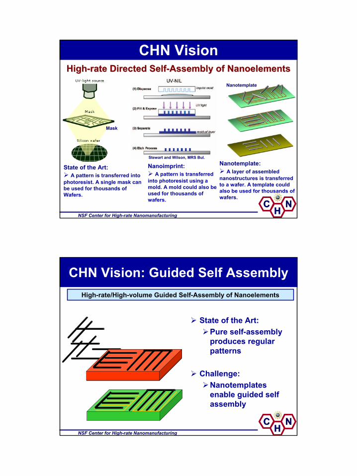
Electrostatic Assembly of Nanoparticles
bright field dark field
Assembly of 300 nm PSL particles (negatively charged) on positively-charged Au microwires
Computational fluid dynamic (CFD) model to aid in preparing templates with uniform deposition
The dependence of surface charge on particle size and mol concentration of liquid.
1.E-10
1.E-091.E-081.E-07
1.E-061.E-051.E-04
1.E-03
1.E-02
1.E+00 1.E+01 1.E+02 1.E+03
Particle Radius R (nm)
q/(4πε rε 0Ψ
0) 10-7 M10-5 M10-3 M10-1 M1 M
dark field bright fieldPSL Fluorescent Particles
Microfingers on the template.
Current Template size is:
2.25 - 4.00 cm2
NSF Center for High-rate Nanomanufacturing
C NH
C NH
Electrostatic Assembly of Nanoparticles
50 nm PSL particles assembled in trenches. (left) partial coverage in 260 nm wide trenches at 2 V for 30 seconds; (right) full coverage
in 260 nm wide trenches at 3 V DC for 90 seconds.
50 nm PSL nanoparticles assembly in multi-layers50 nm particle assembly in a monolayer
6
NSF Center for High-rate Nanomanufacturing
C NH
C NH
Electrostatic Assembly of Nanoparticles
10-15 nm silica nanoparticles in 30 nm trenches
50 nm PSL nanoparticles in 50 nm trenches
NSF Center for High-rate Nanomanufacturing
C NH
C NH
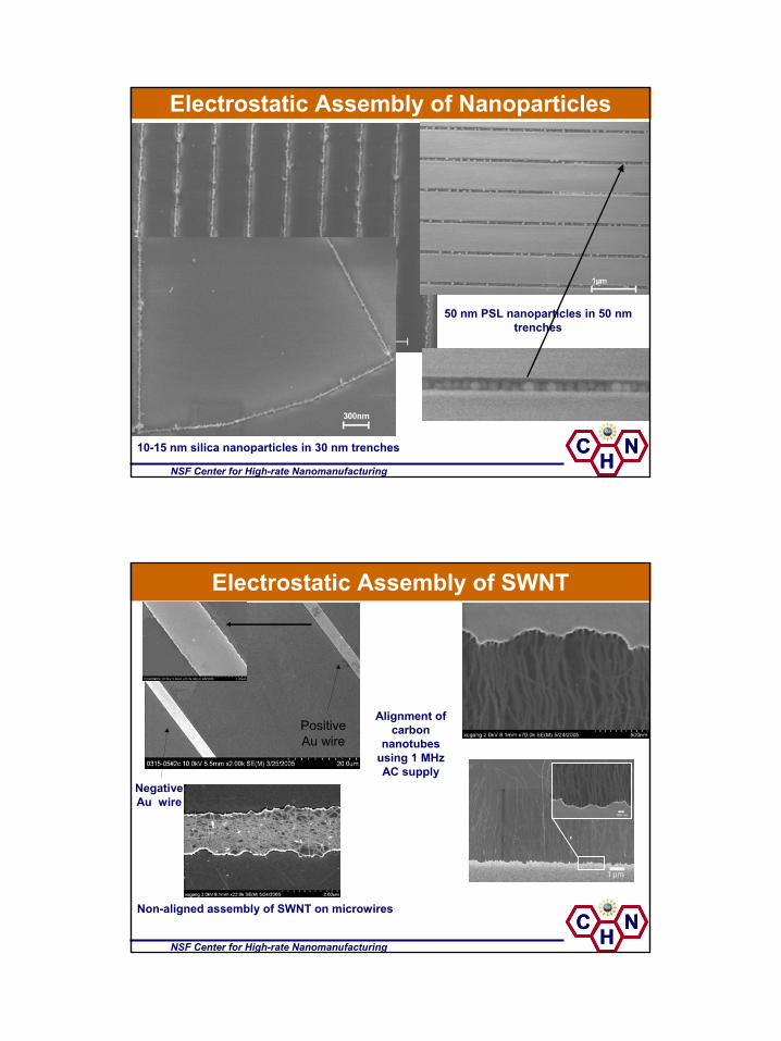
Electrostatic Assembly of SWNT
Positive Au wire
Negative Au wire
Non-aligned assembly of SWNT on microwires
Alignment of carbon
nanotubes using 1 MHz AC supply

7
NSF Center for High-rate Nanomanufacturing
C NH
C NH
Electrostatic Assembly of SWNT in Trenches
Assembly into sub 100 nm trenches with 5 V for 1 minute
SWNTs Assembled within polymer trenches SWNT on gold after dissolving polymer
NSF Center for High-rate Nanomanufacturing
C NH
C NH
Polymer A + B Blends/block copolymers
Nanotemplates used as tooling surface in high
rate process
a b
Highlights of Guided Self-Assembly of Polymer Melts at High Rates
Injection Molder
Use nanotemplates in high rate environment
microinjection molding machine
Complex shapes can be manufactured
8
NSF Center for High-rate Nanomanufacturing
C NH
C NH
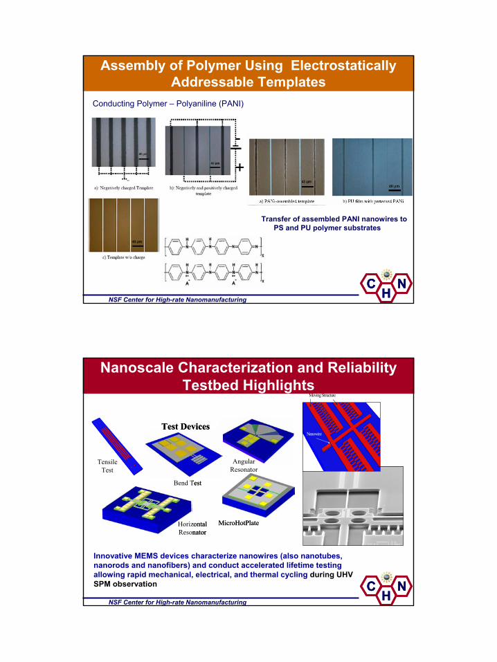
Assembly of Polymer Using Electrostatically Addressable Templates
-
+
Conducting Polymer – Polyaniline (PANI)
Transfer of assembled PANI nanowires to PS and PU polymer substrates
NSF Center for High-rate Nanomanufacturing
C NH
C NH
Nanoscale Characterization and Reliability Testbed Highlights
Nanowire
Moving Structure
Test Devices
Tensile Test
Bend Test
Horizontal Resonator
MicroHotPlate
Angular Resonator
Test Devices
Tensile Test
Bend Test
Horizontal Resonator
MicroHotPlate
Angular Resonator
Innovative MEMS devices characterize nanowires (also nanotubes, nanorods and nanofibers) and conduct accelerated lifetime testing allowing rapid mechanical, electrical, and thermal cycling during UHV SPM observation

9
NSF Center for High-rate Nanomanufacturing
C NH
C NH
High Density Memory ChipCurrent process
Uses conventional optical lithography to pattern carbon nanotube films
Switches are made from belts (ribbons) of nanotubes
Electrodes(~100nm
with 300 nm period)
ON state
OFF state
Nanotemplate will enable single CNT electromechanical switch
(Nantero, 2004)
NSF Center for High-rate Nanomanufacturing
C NH
C NH
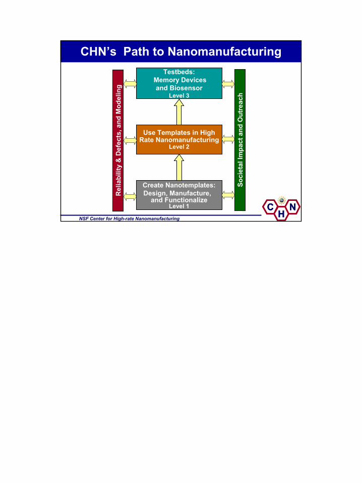
Q1b. How does concept design translate into high-rate manufacturing and how is it validated through the testbeds?
Testbeds:Memory Devicesand Biosensor
Use Templates in High Rate
Nanomanufacturing
Create Nanotemplates:Design, Manufacture,
and Functionalize
Carbon nanotubes assembled from solution
Carbon nanotubeon silicon trenches
Use Templates in High Rate Nanomanufacturing
Testbeds:Memory Devicesand Biosensor

10
NSF Center for High-rate Nanomanufacturing
C NH
C NH
High Volume Wet Chemical Synthesis of SWNTs with Uniform, Tunable Properties
SWNTs with Controllable Diameters and lengths
1.
2.
Cyclacene precursors, both acenes and fullerene-acene adducts, have been synthesized.
cyclacene
NSF Center for High-rate Nanomanufacturing
C NH
C NH
Full systems analysis to assess technology development of nanotemplating
Create environmentally benign processes and products
Identify significant cost barriers
Inform policymakers and generate public discourse during process development
Establish comprehensive assessment practices for success of technology
Concurrent Assessment Processes
EngineeringAssessment
Nano ProcessDesign
Combined Assessment of
DesignTradeoffs
Project 9
Projects 1 -8EngineeringAssessment
Nano Process
Development
Comprehensive Assessment of
DesignTradeoffs
EnvironmentalAssessment
EconomicAssessment
Ethical/ RegulatoryAssessment
EnvironmentalAssessment
Economic Assessment
Ethical/ Regulatory Assessment
Societal IssuesAdvisory
Committee
Societal ImpactAnd
Outreach

11
NSF Center for High-rate Nanomanufacturing
C NH
C NH
Partnerships
FacilitiesResearchers
StudentsFaculty
FacultyResearchersStudents
FacultyResearchersStudents
Industry
Wolfe Laboratories, Inc.
Universities and other OutreachHAMPTON UNIVERSITYHAMPTON UNIVERSITY
Government Labs
C NH
C NH
NSF Center for High-rate Nanomanufacturing
C NH
C NH
Team Strength and SynergyNEU
MEMS, fabrication, nanoscale contamination control
UMLHigh volume polymer processing
Semiconductor & MEMs fab10,000 ft2 class 10 and 100 cleanroom6 inch completer Wafer fab, nanolithography capabilities
UNHSynthesis, self-assembly
Fully-equipped synthetic labs 10,000 ft2 +
Plastics processing labs40,000 ft2 +Compounding, and forming equipment
Characterization labs at NEU, UNH and UML:material characterization and analysis including STM/AFM, NSOM,
SIMS, SEM, TEM, XRD, AEM, XPS,
A unique partnership
C NH
C NH
12
NSF Center for High-rate Nanomanufacturing
C NH
C NH
Testbeds:Memory Devicesand Biosensor
Level 3
Create Nanotemplates:Design, Manufacture,
and FunctionalizeLevel 1
Rel
iabi
lity
& D
efec
ts, a
nd M
odel
ing
Soci
etal
Impa
ct a
nd O
utre
ach
Use Templates in High Rate Nanomanufacturing
Level 2
CHN’s Path to Nanomanufacturing