Embed Size (px)
Citation preview
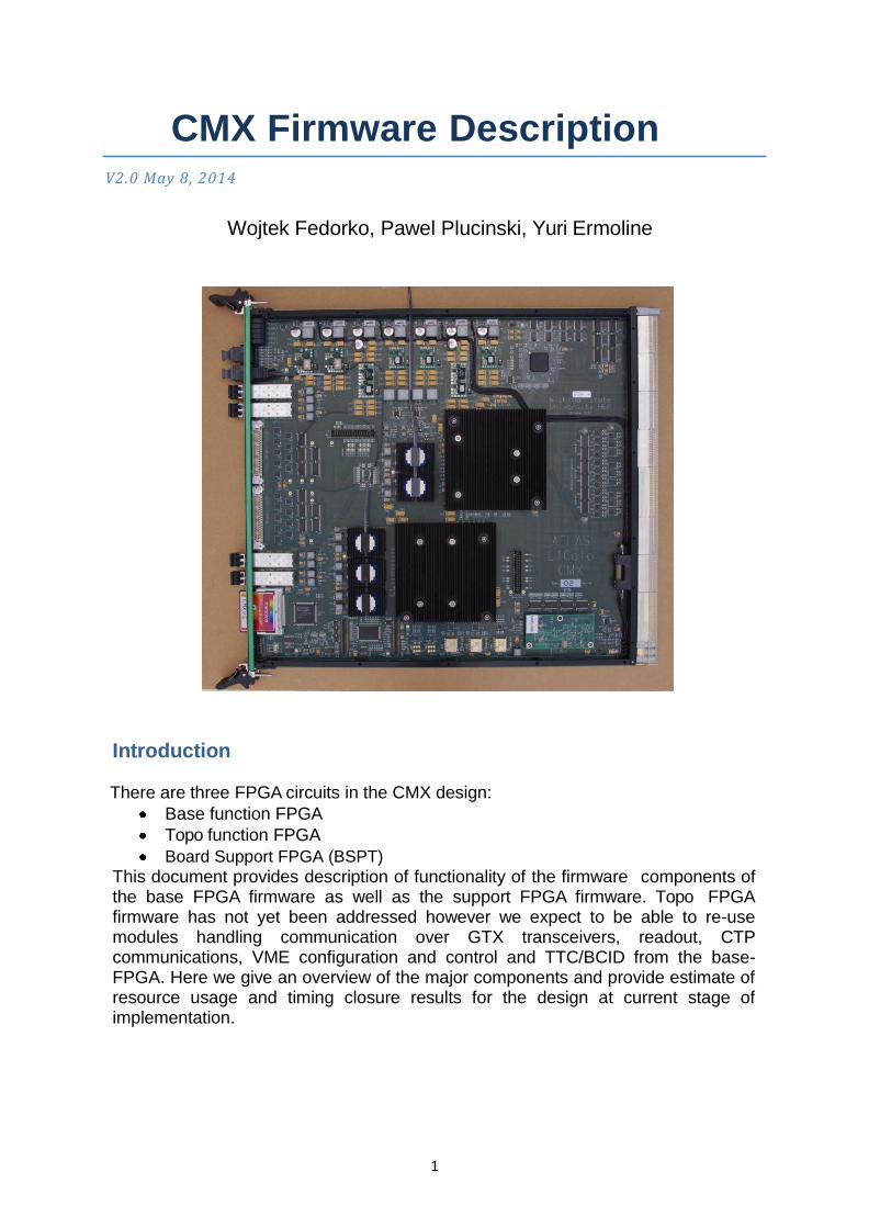
1
CMX Firmware Description V2.0 May 8, 2014
Wojtek Fedorko, Pawel Plucinski, Yuri Ermoline
Introduction
There are three FPGA circuits in the CMX design:
Base function FPGA
Topo function FPGA
Board Support FPGA (BSPT) This document provides description of functionality of the firmware components of the base FPGA firmware as well as the support FPGA firmware. Topo FPGA firmware has not yet been addressed however we expect to be able to re-use modules handling communication over GTX transceivers, readout, CTP communications, VME configuration and control and TTC/BCID from the base- FPGA. Here we give an overview of the major components and provide estimate of resource usage and timing closure results for the design at current stage of implementation.
2
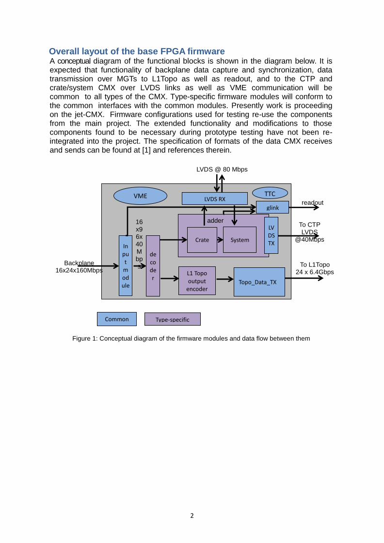
Overall layout of the base FPGA firmware A conceptual diagram of the functional blocks is shown in the diagram below. It is expected that functionality of backplane data capture and synchronization, data transmission over MGTs to L1Topo as well as readout, and to the CTP and crate/system CMX over LVDS links as well as VME communication will be common to all types of the CMX. Type-specific firmware modules will conform to the common interfaces with the common modules. Presently work is proceeding on the jet-CMX. Firmware configurations used for testing re-use the components from the main project. The extended functionality and modifications to those components found to be necessary during prototype testing have not been re-integrated into the project. The specification of formats of the data CMX receives and sends can be found at [1] and references therein.
Input
module
decoder
LVDS RX
Topo_Data_TX
L1 Topo output
encoder
adder
Crate System
glink emulato
r LVDS TX
LVDS @ 80 Mbps
Backplane 16x24x160Mbps
To CTP LVDS
@40Mbps
To L1Topo 24 x 6.4Gbps
16x96x40Mbps
readout
Common to all
flavors
Type-specific
Figure 1: Conceptual diagram of the firmware modules and data flow between them
VME TTC
3
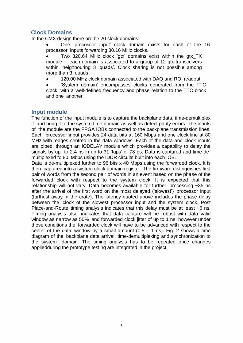
Clock Domains In the CMX design there are be 20 clock domains:
One ‘processor input’ clock domain exists for each of the 16 processor inputs forwarding 80.16 MHz clocks.
Two 320.64 MHz clock ‘gtx’ domains exist within the gtx_TX module – each domain is associated to a group of 12 gtx transceivers within neighbouring 3 ‘quads’. Clock sharing is not possible among more than 3 quads
120.00 MHz clock domain associated with DAQ and ROI readout
‘System domain’ encompasses clocks generated from the TTC clock with a well-defined frequency and phase relation to the TTC clock and one another.
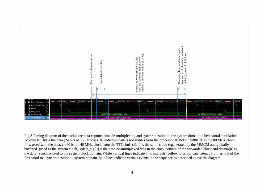
Input module The function of the input module is to capture the backplane data, time-demultiplex it and bring it to the system time domain as well as detect parity errors. The inputs of the module are the FPGA IOBs connected to the backplane transmission lines. Each processor input provides 24 data bits at 160 Mbps and one clock line at 80 MHz with edges centred in the data windows. Each of the data and clock inputs are piped through an IODELAY module which provides a capability to delay the signals by up to 2.4 ns in up to 31 ‘taps’ of 78 ps. Data is captured and time de-multiplexed to 80 Mbps using the IDDR circuits built into each IOB. Data is de-multiplexed further to 96 bits x 40 Mbps using the forwarded clock. It is then captured into a system clock domain register. The firmware distinguishes first pair of words from the second pair of words in an event based on the phase of the forwarded clock with respect to the system clock. It is expected that this relationship will not vary. Data becomes available for further processing ~35 ns after the arrival of the first word on the most delayed (‘slowest’) processor input (furthest away in the crate). The latency quoted above includes the phase delay between the clock of the slowest processor input and the system clock. Post Place-and-Route timing analysis indicates that this delay must be at least ~6 ns. Timing analysis also indicates that data capture will be robust with data valid window as narrow as 50% and forwarded clock jitter of up to 1 ns, however under these conditions the forwarded clock will have to be advanced with respect to the center of the data window by a small amount (0.5 – 1 ns). Fig. 2 shows a time diagram of the backplane data arrival, time-demultiplexing and synchronization to the system domain. The timing analysis has to be repeated once changes appliedduring the prototype testing are integrated in the project.
4
Fir
st w
ord
in
the
even
t ar
rives
Dat
a val
id w
indow
(3
ns)
Lat
ency
bet
wee
n a
rriv
al o
f th
e fi
rst
word
and
synch
roniz
atio
n o
f th
e 40
Mbps
dat
a to
syst
em d
om
ain (
30.4
ns)
Phas
e del
ay between’slowest’
sou
rce
syn
chro
nous
clock
and
(re
cover
ed a
nd
buff
ered
) sy
stem
clo
ck (
2.8
ns)
Fig 2 Timing diagram of the backplane data capture, time de-multiplexing and synchronization to the system domain in behavioral simulation.
BckplnDatCh0 is the data (24 bits at 160 Mbps) (‘X’ indicates data is not stable) from the processor 0, BckplClk80Ch0 is the 80 MHz clock
forwarded with the data, clk40 is the 40 MHz clock from the TTC, buf_clk40 is the same clock regenerated by the MMCM and globally
buffered (used as the system clock), odata_sig[0] is the time de-multiplexed data in the clock domain of the forwarded clock and data96[0] is
the data synchronized to the system clock domain. White vertical lines indicate 5 ns intervals, yellow lines indicate latency from arrival of the
first word to synchronization to system domain, blue lines indicate various events in the sequence as described above the diagram.
5
Topo_Data_TX module This module implements 24 GTX transmitters operating at 6.4Gbps line rate each (5.12 Gbps data rate). In each bunch crossing 3072 bits are transmitted (128 per gtx TX). Data is supplied to the module in the system 40.08 MHz domain. It is then serialized to 320 Mbps still in the system domain. Serialization is performed in parallel for sections of the input data that will be loaded onto separate GTXs thus forming 24 320 Mbps bytestreams. During the serialization control characters are added for less busy events. Following serialization CRC is attached to each bytestream.
Two internal clock domains are necessary, each operating at 320.64 MHz. The reference clocks are shared among two groups of three transciever ‘quads’. GTX transmitters implement 8b/10b encoding with 20 bit internal data width (16 bit user data width). Bytestreams are individually transferred to the GTX TX domains using low latency custom FIFOs implemented in dual port RAMs
The GTX transmitters are set up to bypass the TX buffer minimizing latency with an added benefit of phase synchronization of the outputs. Depending on parametrized switch in the VHDL code the receiver portion of GTX transceivers is powered and support circuitry instantiated enabling data readout to the top module. Such setup will enable internal PMA loopback tests of the megabit interfaces even though base FPGA will not be instrumented with optical gigabit receivers.
Encoder (jet type) The role of this module is to transform array of TOBs provided by the decoder as well as the BCID information provided by the TTC module and encode this information in the vector provided to the transmitter module. Very little logic is needed in this module – only signal renaming and synchronization of bunch counter into signal into the same register as the TOB data.
Decoder (jet type) The main function of the CMX decoder (see Figure 1) is to fetch the data from the input module, to process it and provide two data streams for the adder and L1Topo Encoder. The output data consists of the trigger objects (TOBs) multiplicities for each of twenty-five thresholds and parity bits for the adder and an array of the trigger objects for the L1Topo output block. The thresholds value is defined by the VME registers. Based on the data analysis, the CMX decoder has to send up to 32 trigger objects to the L1Topo. In addition, in order to reduce the data volume and decrease the time needed to sort the data only non-empty trigger objects are provided. The input data for the decoder consists of 16 channels x 96 bits at 40MHz. The time needed to provide the trigger output is estimated to be only one 40MHz clock cycle.
6
Adder (jet type) The real-time output of the CMX decoder is sent to the adder which consists of two parts that perform crate and system level merging, respectively, at 40.08 MHz. The function of the adder is to receive the trigger objects multiplicities, process it and transmit it to the Central Trigger Processor (CTP).
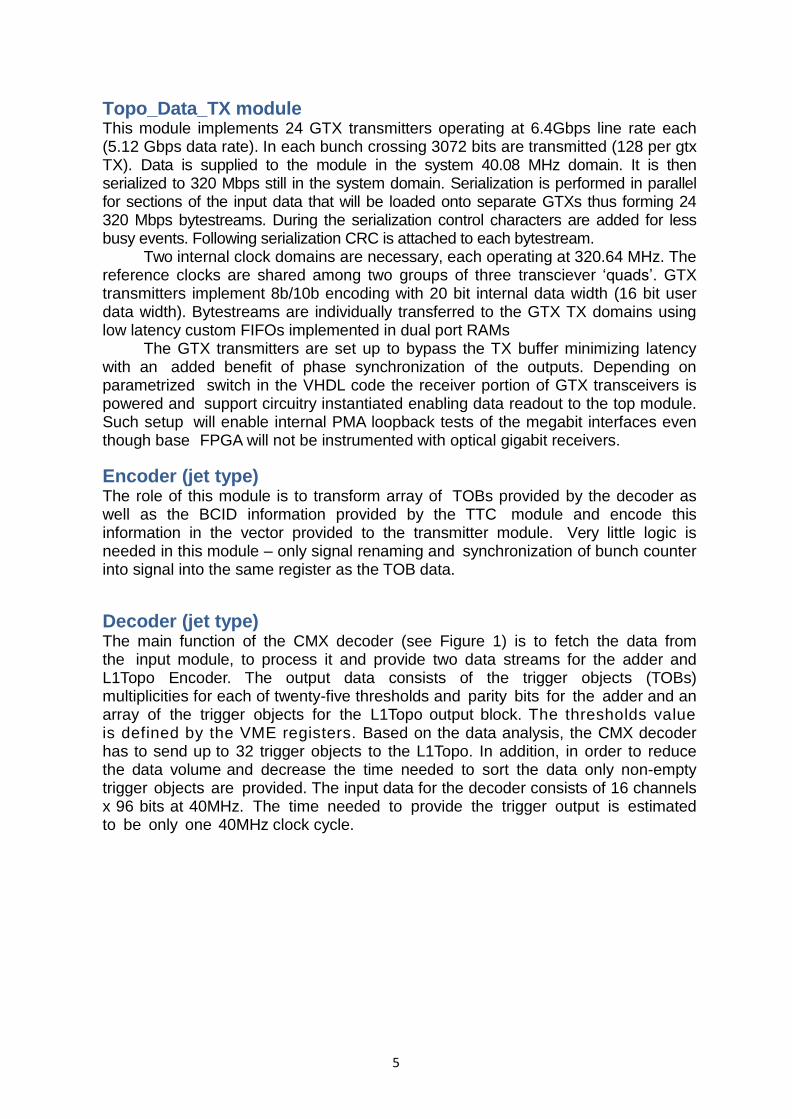
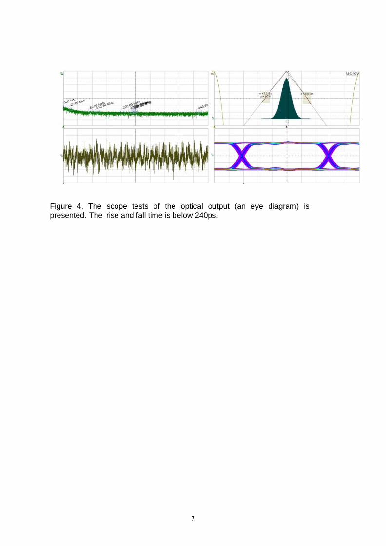
Glink Readout to the DAQ and RoI RODs is carried out by a pair of emulated G-link protocol (Figure 3) in Virtex-6, using GTX transmitters clocked at 960 Mbits/s. The G-Link protocol was successfully implemented and tested in Virtex-6. The scope tests of the optical output (an eye diagram, Figure 4) executed with the evaluation card, proved that there is no problem to emulate the G-link protocol in the FPGA. The rise and fall time was measured below 240 ps, which is sufficient to fulfill the G-link protocol requirements. The CMX G-Link protocol encodes 20 bits of user data. On receipt of an L1A signal, the G-Link control firmware is obliged to extract the data which is connected via a shift register to one of the G-Link emulated user data pins. The internal logic moves the diagnostic data into the shift registers and asserts the Data Available (DAV) signal to the G-Link logic. The Low Speed Optical components then transmit the encoded data from G-link to the RODs. An odd parity bit is appended to each active G-Link line when the shift register contents have been transmitted. The logic then de-asserts the DAV signal and emulated G-Link returns to its quiescent state for a minimum of one clock cycle.
Figure 3. The general idea of emulated G-link protocol in Virtex-6
7
Figure 4. The scope tests of the optical output (an eye diagram) is presented. The rise and fall time is below 240ps.
8
Resource use and timing closure.
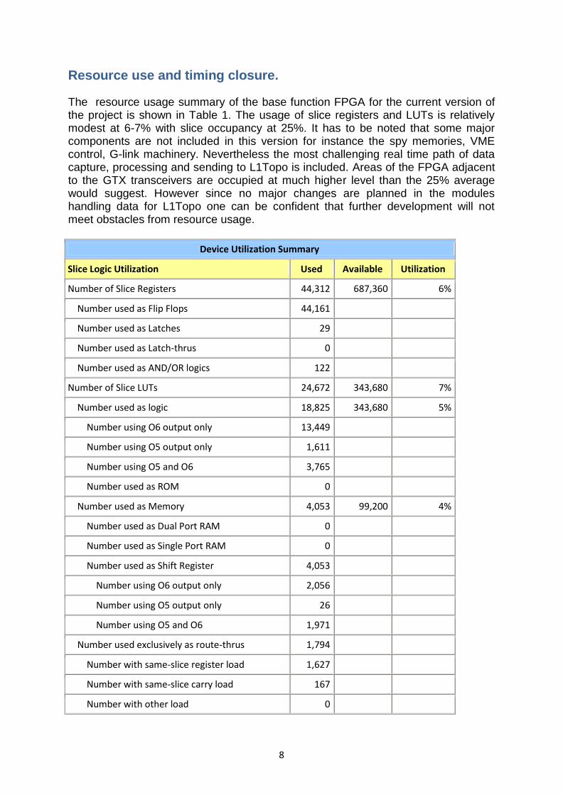
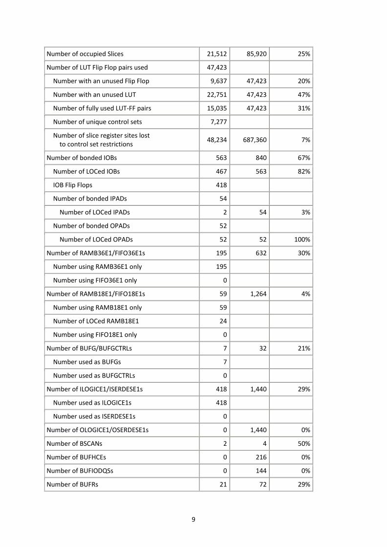
The resource usage summary of the base function FPGA for the current version of the project is shown in Table 1. The usage of slice registers and LUTs is relatively modest at 6-7% with slice occupancy at 25%. It has to be noted that some major components are not included in this version for instance the spy memories, VME control, G-link machinery. Nevertheless the most challenging real time path of data capture, processing and sending to L1Topo is included. Areas of the FPGA adjacent to the GTX transceivers are occupied at much higher level than the 25% average would suggest. However since no major changes are planned in the modules handling data for L1Topo one can be confident that further development will not meet obstacles from resource usage.
Device Utilization Summary
Slice Logic Utilization Used Available Utilization
Number of Slice Registers 44,312 687,360 6%
Number used as Flip Flops 44,161
Number used as Latches 29
Number used as Latch-thrus 0
Number used as AND/OR logics 122
Number of Slice LUTs 24,672 343,680 7%
Number used as logic 18,825 343,680 5%
Number using O6 output only 13,449
Number using O5 output only 1,611
Number using O5 and O6 3,765
Number used as ROM 0
Number used as Memory 4,053 99,200 4%
Number used as Dual Port RAM 0
Number used as Single Port RAM 0
Number used as Shift Register 4,053
Number using O6 output only 2,056
Number using O5 output only 26
Number using O5 and O6 1,971
Number used exclusively as route-thrus 1,794
Number with same-slice register load 1,627
Number with same-slice carry load 167
Number with other load 0
9
Number of occupied Slices 21,512 85,920 25%
Number of LUT Flip Flop pairs used 47,423
Number with an unused Flip Flop 9,637 47,423 20%
Number with an unused LUT 22,751 47,423 47%
Number of fully used LUT-FF pairs 15,035 47,423 31%
Number of unique control sets 7,277
Number of slice register sites lost to control set restrictions
48,234 687,360 7%
Number of bonded IOBs 563 840 67%
Number of LOCed IOBs 467 563 82%
IOB Flip Flops 418
Number of bonded IPADs 54
Number of LOCed IPADs 2 54 3%
Number of bonded OPADs 52
Number of LOCed OPADs 52 52 100%
Number of RAMB36E1/FIFO36E1s 195 632 30%
Number using RAMB36E1 only 195
Number using FIFO36E1 only 0
Number of RAMB18E1/FIFO18E1s 59 1,264 4%
Number using RAMB18E1 only 59
Number of LOCed RAMB18E1 24
Number using FIFO18E1 only 0
Number of BUFG/BUFGCTRLs 7 32 21%
Number used as BUFGs 7
Number used as BUFGCTRLs 0
Number of ILOGICE1/ISERDESE1s 418 1,440 29%
Number used as ILOGICE1s 418
Number used as ISERDESE1s 0
Number of OLOGICE1/OSERDESE1s 0 1,440 0%
Number of BSCANs 2 4 50%
Number of BUFHCEs 0 216 0%
Number of BUFIODQSs 0 144 0%
Number of BUFRs 21 72 29%
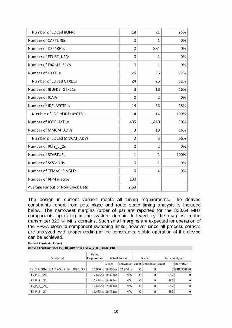
10
Number of LOCed BUFRs 18 21 85%
Number of CAPTUREs 0 1 0%
Number of DSP48E1s 0 864 0%
Number of EFUSE_USRs 0 1 0%
Number of FRAME_ECCs 0 1 0%
Number of GTXE1s 26 36 72%
Number of LOCed GTXE1s 24 26 92%
Number of IBUFDS_GTXE1s 3 18 16%
Number of ICAPs 0 2 0%
Number of IDELAYCTRLs 14 36 38%
Number of LOCed IDELAYCTRLs 14 14 100%
Number of IODELAYE1s 435 1,440 30%
Number of MMCM_ADVs 3 18 16%
Number of LOCed MMCM_ADVs 2 3 66%
Number of PCIE_2_0s 0 2 0%
Number of STARTUPs 1 1 100%
Number of SYSMONs 0 1 0%
Number of TEMAC_SINGLEs 0 4 0%
Number of RPM macros 130
Average Fanout of Non-Clock Nets 2.63
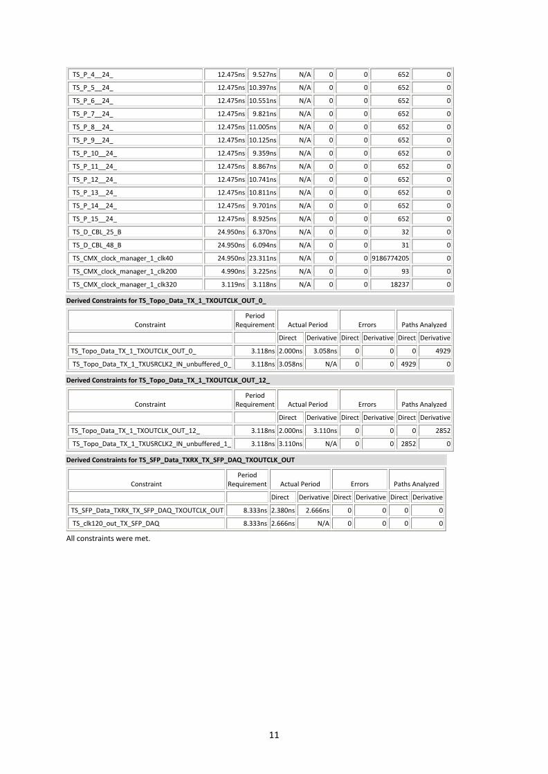
The design in current version meets all timing requirements. The derived constraints report from post place and route static timing analysis is included below. The narrowest margins (order of ps) are reported for the 320.64 MHz components operating in the system domain followed by the margins in the transmitter 320.64 MHz domains. Such small margins are expected for operation of the FPGA close to component switching limits, however since all process corners are analyzed, with proper coding of the constraints, stable operation of the device can be achieved.
Derived Constraint Report
Derived Constraints for TS_CLK_40MHz08_DSKW_2_BF_LOGIC_DIR
Constraint Period
Requirement Actual Period Errors Paths Analyzed
Direct Derivative Direct Derivative Direct Derivative
TS_CLK_40MHz08_DSKW_2_BF_LOGIC_DIR 24.950ns 10.000ns 24.944ns 0 0 0 9186803030
TS_P_0__24_ 12.475ns 10.477ns N/A 0 0 652 0
TS_P_1__24_ 12.475ns 10.665ns N/A 0 0 652 0
TS_P_2__24_ 12.475ns 9.041ns N/A 0 0 652 0
TS_P_3__24_ 12.475ns 10.791ns N/A 0 0 652 0
11
TS_P_4__24_ 12.475ns 9.527ns N/A 0 0 652 0
TS_P_5__24_ 12.475ns 10.397ns N/A 0 0 652 0
TS_P_6__24_ 12.475ns 10.551ns N/A 0 0 652 0
TS_P_7__24_ 12.475ns 9.821ns N/A 0 0 652 0
TS_P_8__24_ 12.475ns 11.005ns N/A 0 0 652 0
TS_P_9__24_ 12.475ns 10.125ns N/A 0 0 652 0
TS_P_10__24_ 12.475ns 9.359ns N/A 0 0 652 0
TS_P_11__24_ 12.475ns 8.867ns N/A 0 0 652 0
TS_P_12__24_ 12.475ns 10.741ns N/A 0 0 652 0
TS_P_13__24_ 12.475ns 10.811ns N/A 0 0 652 0
TS_P_14__24_ 12.475ns 9.701ns N/A 0 0 652 0
TS_P_15__24_ 12.475ns 8.925ns N/A 0 0 652 0
TS_D_CBL_25_B 24.950ns 6.370ns N/A 0 0 32 0
TS_D_CBL_48_B 24.950ns 6.094ns N/A 0 0 31 0
TS_CMX_clock_manager_1_clk40 24.950ns 23.311ns N/A 0 0 9186774205 0
TS_CMX_clock_manager_1_clk200 4.990ns 3.225ns N/A 0 0 93 0
TS_CMX_clock_manager_1_clk320 3.119ns 3.118ns N/A 0 0 18237 0
Derived Constraints for TS_Topo_Data_TX_1_TXOUTCLK_OUT_0_
Constraint Period
Requirement Actual Period Errors Paths Analyzed
Direct Derivative Direct Derivative Direct Derivative
TS_Topo_Data_TX_1_TXOUTCLK_OUT_0_ 3.118ns 2.000ns 3.058ns 0 0 0 4929
TS_Topo_Data_TX_1_TXUSRCLK2_IN_unbuffered_0_ 3.118ns 3.058ns N/A 0 0 4929 0
Derived Constraints for TS_Topo_Data_TX_1_TXOUTCLK_OUT_12_
Constraint Period
Requirement Actual Period Errors Paths Analyzed
Direct Derivative Direct Derivative Direct Derivative
TS_Topo_Data_TX_1_TXOUTCLK_OUT_12_ 3.118ns 2.000ns 3.110ns 0 0 0 2852
TS_Topo_Data_TX_1_TXUSRCLK2_IN_unbuffered_1_ 3.118ns 3.110ns N/A 0 0 2852 0
Derived Constraints for TS_SFP_Data_TXRX_TX_SFP_DAQ_TXOUTCLK_OUT
Constraint Period
Requirement Actual Period Errors Paths Analyzed
Direct Derivative Direct Derivative Direct Derivative
TS_SFP_Data_TXRX_TX_SFP_DAQ_TXOUTCLK_OUT 8.333ns 2.380ns 2.666ns 0 0 0 0
TS_clk120_out_TX_SFP_DAQ 8.333ns 2.666ns N/A 0 0 0 0
All constraints were met.
12
Board Support FPGA (BSPT) Firmware Introduction Ancillary tasks which are not part of the real-time operation of the CMX card are implemented in a separate smaller FPGA called the Board Support FPGA (BSPT). The device chosen for the BSPT FPGA is a Xilinx Spartan-3A XC3S400A in the 400 pin FG400 package. The Board Control FPGA is responsible for:
controlling of the System ACE and configuration of the main FPGAs,
controlling and monitoring the operation of the TTCrx chip on the TTCDec,
controlling and monitoring the MiniPOD transmitters and receivers,
controlling and monitoring the SFP optical modules,
presenting registers in VME-- space to access all above features,
controlling the data bus transceivers to the VME—bus,
generating DTACK_B during VME-- Cycles,
detecting the presence of and configuration of the BF and TP FPGA,
provide logic as part of the hardwired Transceiver Control Oversight (below),
controlling all the front-panel LEDs except one (power). On power up the BSPT FPGA configures itself using its attached serial configuration PROM. Updating the BSPT firmware requires using the Test JTAG Chain (accessible through the front-panel test connector) to load the new firmware directly into the BSPT FPGA or load it into the BSPT serial configuration PROM device. The BSPT FPGA FW description is in: http://www.pa.msu.edu/hep/atlas/l1calo/cmx/firmware/fpga_bspt_fw/
Development and test The implementation of the BSPT FPGA firmware (FW) is based on CMM and JEM designs. From CMM design the FW for the following hardware parts was used:
non-volatile VME CPLD (XCR3384XL-10FT256C) which contains some basic registers in a case of a malfunction in the FPGA configuration process,
TTC FPGA (XCV100E-6FG256C), which provides an access to the CMM TTC daughter card.
From JEM design the FW for the control CPLD (XC2C128_TQ144), which provides access to the CMM XILINX System ACE controller, was used. For the test purposes these VHDL codes were merged in a single design, implemented in Spartan-3AN FPGA - XC3S200AN-FTG256 and tested on the VAT card. The VAT card is a test card in 6U VME form factor which implements the interface to the ACE and TTC sub-sections and includes a small Virtex-6 FPGA device as a target for configuration. The VAT card has been used to design the VME Interface Firmware and practice controlling the System ACE, the TTCrx chip on the TTCDec mezzanine card and configuration of the Virtex-6 FPGA.
13
For the CMX, this firmware was adapted to the actual CMX hardware and augmented with extra functionalities for the optical components and CMX auxiliary logic.
CMX BSPT FPGA VME-- address map The CMX VME-- memory map allocates 0x80000 bytes for each CMX (512k):
CMX0 (slot 3): 0x700000 - 0x77FFFE
CMX1 (slot 20): 0x780000 - 0x7FFFFE The first 256 bytes are allocated for the BSPT FPGA (0x0000 - 0x00FF). This address space is used as follow:
0x00 - 0x0E – common module registers and LVDS Links management
0x10 - 0x26 – optical components access via I2C interface,
0x30 - 0x5E – access to the TTCrx chip on the TTCDec card,
0x80 - 0xDE – access to the XILINX System ACE chip. All unused addresses are reserved, some of them used to implement the test registers. To test the reliability of the access to the internal registers from VME a sophisticated program in Python was written by Philippe Laurens. The BSPT FPGA memory map and detailed register description for the second FW revision is in chapter 2 of the vme_map_v2_20140417.txt file: http://www.pa.msu.edu/hep/atlas/l1calo/cmx/firmware/fpga_bspt_fw/vme_map_v2_20140417.txt
Common module registers and LVDS Links management: 00 RO Module ID and SN 02 RO Module HW/FW Revisions 04 RW Module Control Register 06 RW Module Resets Register 08 RO Module Status 1 0A RO Module Status 2 0C RO LVDS Link Status 1 0E RO LVDS Link Status 2 For the LVDS links, the management of the control signals to the LVDS transceivers comes from the BSPT FPGA. In turn the BSPT FPGA listens to signals from the BF and TP FPGAs to learn how they want the various LVDS transceivers configured, i.e. as inputs or as outputs. The status of all signals (coming from the BF and TP FPGAs and generated by the BSPT FPGA) can be accessed via two status registers 0C and 0E
Optical components access via I2C interface: 10 RW SFP1 Control/Status Register 12 RW SFP1 Data Register 14 RW SFP2 Control/Status Register 16 RW SFP2 Data Register
14
18 RW SFP3 Control/Status Register 1A RW SFP3 Data Register 1C RW SFP4 Control/Status Register 1E RW SFP4 Data Register 20 RW MP12 Control/Status Register 22 RW MP12 Data Register 24 RW MP345 Control/Status Register 26 RW MP345 Data Register Access to the internal registers of the optical components (SFP and MiniPOD) is provided via I2C interface to pair of registers: Control/Status Register and Data Register. To WRITE the data into writable internal register of the optical component:
write data to bits 15-8 of the Data Register
write control data to the Control/Status Register To READ the data from the internal register of the optical component:
write control data to the Control/Status Register
read the data from bits 7-0 of the Data Register
Access to the TTCrx chip on the TTCDec card: 30 RW TTCrx Control Register 32 RO TTCrx Status Register 34 RO TTCDec Brcst Register 36 RO TTCDec DQ Register 40 RO TTCDec Dump RAM addresses from 00040 to 0005E Acces to the TTCrx chip on the TTCDEC card is provided via TTCrx Control Register and TTCrx Status Register (as in CMM). Detailed description of the TTCrx chip access is in: http://www.pa.msu.edu/hep/atlas/l1calo/cmx/firmware/fpga_bspt_fw/TTCrx_control_draft.txt
Access to the XILINX System ACE chip: 80 to DF ->See XILINX System ACE The XILINX System ACE controller internal registers are mapped to the VME adresses (See System ACE CompactFlash Solution, DS080 (v2.0) October 1, 2008)
Current status The design of the BSPT FPGA firmware is completed. It may undergo some small adjustment during the final production and test of the CMX cards and development of the BASE and TOPO FPGAs firmware. It was implemented on XILINX ISE 13.4, the results are shown below:
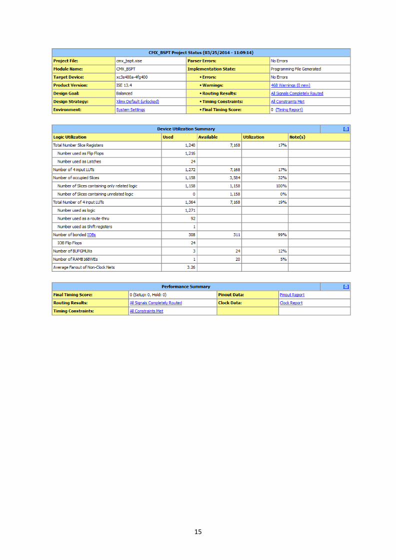
15
16
References: [1] https://twiki.cern.ch/twiki/bin/view/Atlas/L1CaloUpgrade#New_data_transfer_and_readout_fo