Embed Size (px)
Citation preview
Tom Penick [email protected] www.teicontrols.com/notes 1/14/2001 Page 1 of 23
SOLID STATE ELECTRONIC DEVICES EE339
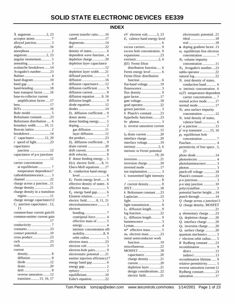
INDEX
Å angstrom.................2, 23 acceptor atoms ................. 7 alloyed junction................ 3 alpha...............................16 amorphous ....................... 2 angstrom .....................2, 23 angular momentum........... 5 annealing ......................... 3 avalanche breakdown ......14 Avogadro's number..........23 Balmer............................. 4 band diagram ..................10 band gap .......................... 6 band-bending ..................18 base transport factor ........16 base-to-collector current
amplification factor .....17 beta.................................17 BJTs ...............................16 Bohr model ...................... 5 Boltzmann constant .........23 Boltzmann distribution..... 6 boundary width .........10, 11 Bravais lattice .................. 2 breakdown ......................14 C capacitance ...........12, 20 c speed of light...............23 capacitance
junction ......................12 capacitance of p-n junctions
...................................12 carrier concentration
at equilibrium .............. 7 temperature dependence7
cathodoluminescence........ 3 channel ...........................22 charge across a junction...11 charge density .................21 charge density in a transition
region .........................11 charge storage capacitance12 Cj junction capacitance.. 12,
13 common-base current gain16 common-emitter current gain
...................................17 conductivity ..................... 7 constants .........................23 contact potential..............10 cross product ...................23 csch ................................23 ctnh.................................23 current
density......................... 8 diffusion ...................... 8 diode ..........................12 drain ...........................20 drift ............................. 8 reverse saturation........12 transistor......... 15, 16, 17
current transfer ratio........16 cutoff ..............................17 degenerate.......................14 del ..................................22 density of states................ 6 dependent wave function .. 4 depletion charge..............20 depletion layer capacitance
...................................12 depletion layer width.......21 diffused junction .............. 3 diffusion .........................16 diffusion capacitance.......12 diffusion coefficient ......... 9 diffusion current............... 8 diffusion equation .......9, 16 diffusion length ................ 9 diode equation.................12 diodes .............................14 Dn diffusion coefficient ... 9 donor atoms ..................... 7 donor binding energy........ 5 doping.............................. 2
gas diffusion ...............11 layer diffusion.............12
dot product......................23 Dp diffusion coefficient ... 9 drain current ...................20 drift current...................... 8 drift velocity..................... 8 E donor binding energy ... 5 E(x) electric field .......8, 11 Ebers-Moll equations ......17 Ec conduction band energy
level ............................ 6 EF Fermi energy level...... 6 effective density of states . 6 effective mass .................. 5 Eg energy band gap.......... 6 Einstein relation............... 7 electric field..........8, 11, 21 electroluminescence ......... 3 electron
bonding........................ 7 centripetal force ........... 4 effective mass of .......... 5 energy.......................... 4 intrinsic concentration of6 mobility ....................8, 9 orbit radius .................. 5
electron mass ..................23 electron volt ..................... 3 electron-hole pairs............ 9 electrostatic potential ......21 emitter injection efficiency17 energy band gap ............... 6 energy gap........................ 2 epitaxy............................. 2 equililbrium....................10 Euler's equation...............22
eV electron volt..........3, 23 Ev valence band energy level
.................................... 6 excess carriers.................. 9 excess hole concentration . 9 expansions ......................23 extrinsic........................2, 6 f(E) Fermi-Dirac
distribution function..... 6 Fermi energy level ........... 6 Fermi-Dirac distribution
function ....................... 6 flat-band voltage .............19 flourescence ..................... 3 flux density...................... 9 gain factor .......................17 gate voltage.....................18 grad operator...................22 grown junction ................. 3 h Planck's constant .........23 hyperbolic functions ........23 hν photon........................ 3 I0 reverse saturation current
...................................12 ID drain current ...............20 interface charge...............20 interface voltage..............19 intrinsic ........................2, 6 intrinsic to Fermi potential
.............................19, 20 inversion .........................21 inversion charge ..............20 inverted mode .................17 ion implantation ............... 3 It transmitted light intensity
.................................... 8 J current density.............. 8 JFET...............................18 k Boltzmann constant .....23 Laplacian ........................23 light ................................. 3 light transmission............. 8 Ln diffusion length........... 9 log function.....................22 Lp diffusion length........... 9 luminescence ................... 3 Lyman.............................. 4 m* effective mass............ 5 m0 electron mass ............23 metal semiconductor work
function ......................19 miscellaneous..................22 MOSFET ........................18
capacitance .................20 charge density.............21 current ........................20 depletion layer ............21 design considerations ..22 electric field................21
electrostatic potential ..21 ideal ...........................18 real .............................18
n doping gradient factor .13 n0 equilibrium free electron
concentration ............... 7 N0 volume impurity
concentration ..............11 NA Avogadro's number....23 nabla operator .................22 natural log.......................22 Nc total density of states,
conduction band........... 6 ni intrinsic concentration . 6 ni(T) temperature-dependent
carrier concentration .... 7 normal active mode .........17 normal mode ...................17 NS area surface impurity
concentration ..............12 Nv total density of states,
valence band................ 6 p+-n junction ...................13 p+-n-p transistor ........15, 16 p0 equilibrium hole
concentration ............... 7 Paschen............................ 4 permittivity of free space.. 5,
23 photo diode .....................14 photoelectric .................... 4 photoluminescence ........... 3 photon.............................. 3 pinch-off voltage .............18 Planck's constant .............23 p-n junctions .................... 3 p-n step junction .............10 polycrystalline.................. 2 potential barrier height....14 punch through .................14 Q charge across a junction11 Q charge density, MOSFET
...................................21 q elementary charge .......23 Qd depletion charge........20 Qi interface charge .........20 Qn inversion charge ........20 Qs surface charge ...........20 quantum mechanics .......... 3 r electron orbit radius...... 5 R Rydberg constant ........23 recombination .................. 9
direct ..........................13 indirect .......................13
recombination lifetime ..... 9 relative permittivity.......... 5 reverse saturation current 12 Rydberg constant.............23 saturation ........................17
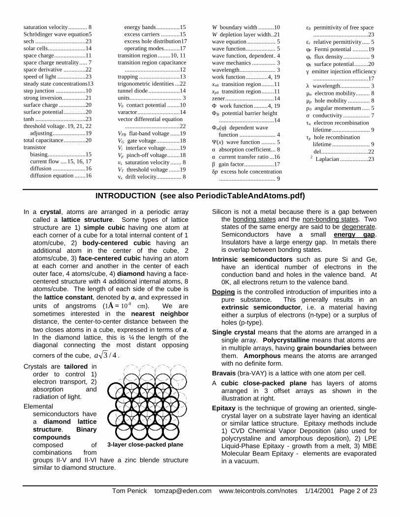
Tom Penick [email protected] www.teicontrols.com/notes 1/14/2001 Page 2 of 23
saturation velocity............ 8 Schrödinger wave equation5 sech ................................23 solar cells........................14 space charge....................11 space charge neutrality..... 7 space derivative ..............22 speed of light ..................23 steady state concentrations13 step junction ...................10 strong inversion...............21 surface charge .................20 surface potential..............20 tanh ................................23 threshold voltage.19, 21, 22
adjusting.....................19 total capacitance..............20 transistor
biasing........................15 current flow .... 15, 16, 17 diffusion .....................16 diffusion equation .......16
energy bands...............15 excess carriers ............15 excess hole distribution17 operating modes..........17
transition region ........10, 11 transition region capacitance
...................................12 trapping ..........................13 trigonometric identities ...22 tunnel diode ....................14 units................................. 3 V0 contact potential ........10 varactor...........................14 vector differential equation
...................................22 VFB flat-band voltage ......19 VG gate voltage...............18 Vi interface voltage.........19 Vp pinch-off voltage........18 vs saturation velocity ....... 8 VT threshold voltage .......19 vx drift velocity................ 8
W boundary width ..........10 W depletion layer width..21 wave equation .................. 5 wave function................... 5 wave function, dependent . 4 wave mechanics ............... 3 wavelength....................... 3 work function..............4, 19 xn0 transition region........11 xp0 transition region........11 zener...............................14 Φ work function .........4, 19 ΦB potential barrier height
...................................14 Φm(φ) dependent wave
function ....................... 4 Ψ(x) wave function ......... 5 α absorption coefficient... 8 α current transfer ratio ...16 β gain factor...................17 δp excess hole concentration
.................................... 9
ε0 permittivity of free space...................................23
εr relative permittivity..... 5 φF Fermi potential ..........19 φn flux density................. 9 φS surface potential.........20 γ emitter injection efficiency
...................................17 λ wavelength................... 3 µn electron mobility......... 8 µp hole mobility .............. 8 ρ0 angular momentum ..... 5 σ conductivity ................. 7 τn electron recombination
lifetime ........................ 9 τp hole recombination
lifetime ........................ 9 ∇ del..............................22 ∇2 Laplacian ..................23
INTRODUCTION (see also PeriodicTableAndAtoms.pdf)
In a crystal, atoms are arranged in a periodic array called a lattice structure. Some types of lattice structure are 1) simple cubic having one atom at each corner of a cube for a total internal content of 1 atom/cube, 2) body-centered cubic having an additional atom in the center of the cube, 2 atoms/cube, 3) face-centered cubic having an atom at each corner and another in the center of each outer face, 4 atoms/cube, 4) diamond having a face-centered structure with 4 additional internal atoms, 8 atoms/cube. The length of each side of the cube is the lattice constant, denoted by a, and expressed in units of angstroms (1Å = 10-8 cm). We are sometimes interested in the nearest neighbor distance, the center-to-center distance between the two closes atoms in a cube, expressed in terms of a. In the diamond lattice, this is ¼ the length of the diagonal connecting the most distant opposing
corners of the cube, 4/3a .
Crystals are tailored in order to control 1) electron transport, 2) absorption and radiation of light.
Elemental semiconductors have a diamond lattice structure. Binary compounds composed of combinations from groups II-V and II-VI have a zinc blende structure similar to diamond structure.
Silicon is not a metal because there is a gap between the bonding states and the non-bonding states. Two states of the same energy are said to be degenerate. Semiconductors have a small energy gap. Insulators have a large energy gap. In metals there is overlap between bonding states.
Intrinsic semiconductors such as pure Si and Ge, have an identical number of electrons in the conduction band and holes in the valence band. At 0K, all electrons return to the valence band.
Doping is the controlled introduction of impurities into a pure substance. This generally results in an extrinsic semiconductor, i.e. a material having either a surplus of electrons (n-type) or a surplus of holes (p-type).
Single crystal means that the atoms are arranged in a single array. Polycrystalline means that atoms are in multiple arrays, having grain boundaries between them. Amorphous means the atoms are arranged with no definite form.
Bravais (bra-VAY) is a lattice with one atom per cell.
A cubic close-packed plane has layers of atoms arranged in 3 offset arrays as shown in the illustration at right.
Epitaxy is the technique of growing an oriented, single-crystal layer on a substrate layer having an identical or similar lattice structure. Epitaxy methods include 1) CVD Chemical Vapor Deposition (also used for polycrystaline and amorphous deposition), 2) LPE Liquid-Phase Epitaxy - growth from a melt, 3) MBE Molecular Beam Epitaxy - elements are evaporated in a vacuum.
3-layer close-packed plane
Tom Penick [email protected] www.teicontrols.com/notes 1/14/2001 Page 3 of 23
Quantum mechanics is a theory of matter that is based on the concept of the possession of wave properties by elementary particles, that affords a mathematical interpretation of the structure and interactions of matter on the basis of these properties, and that incorporates within it quantum theory and the uncertainty principle — called also wave mechanics.
LIGHT Luminescence – the property of light emission Photoluminescence – radiation resulting from the
recombination of carriers excited by photon absorption. Some materials react rapidly to the excitation being turned off; this process is called fluorescence. In other materials, emission continues long after excitation is removed; these processes are called phosphorescence, the materials are phosphors.
Cathodoluminescence – radiation resulting from the recombination of excited carriers created by high-energy electron bombardment.
Electroluminescence – radiation resulting from the recombination of carriers excited by the introduction of current into the sample. The injection electroluminescence effect occurs when an electric current causes the injection of minority carriers into regions of the semiconductor crystal where they can recombine with majority carriers, resulting in recombination radiation—used in LEDs.
P-N JUNCTION FABRICATION Grown – A junction is created by abruptly changing the
doping during the growth of the crystal. Alloyed – A pellet on one material is melted into an
oppositely-doped material and a regrown crystal region forms at the junction.
Diffused – The crystal is heated to about 1000ºC causing atoms to move out of their lattice positions. Doping atoms in a gaseous state outside the material move into the vacated positions by diffusion. This methods offers precision and is implemented in integrated circuit fabrication.
Ion Implantation – A beam of impurity ions is accelerated to a kinetic energy in the range of several KeV to several MeV and fired into the crystal. The depth at which the ions come to rest can be controlled by the kinetic energy level. Used in integrated circuits. Damage to the lattice caused by ion collisions can be repaired by annealing, or heating of the crystal.
BE CAREFUL WITH UNITS! In this course, energy is usually expressed in eV rather
than J, and distance is often cm rather than m. Be sure to be consistent with units in a formula, paying attention to the units of constants as well. Some formulas just do not work with units of eV; calculate energy in J and convert to eV.
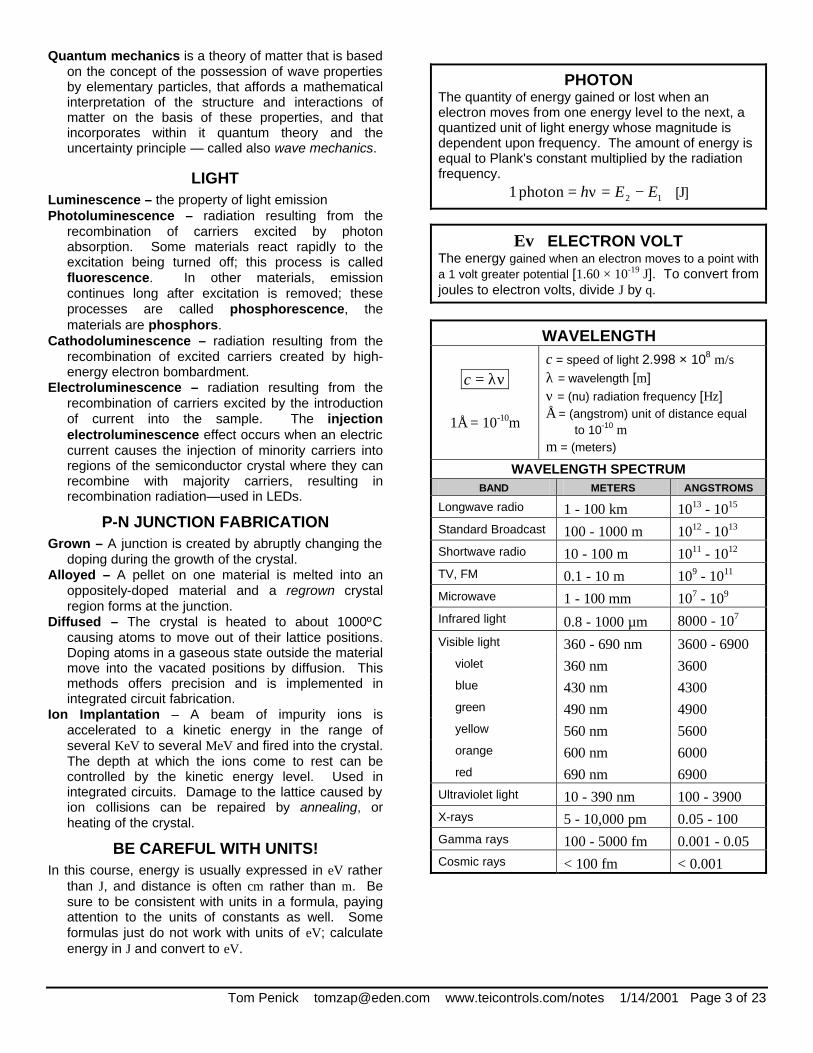
PHOTON The quantity of energy gained or lost when an electron moves from one energy level to the next, a quantized unit of light energy whose magnitude is dependent upon frequency. The amount of energy is equal to Plank's constant multiplied by the radiation frequency.
12photon 1 EEh −=ν= [J]
Ev ELECTRON VOLT The energy gained when an electron moves to a point with a 1 volt greater potential [1.60 × 10⁻¹⁹ J]. To convert from joules to electron volts, divide J by q.
WAVELENGTH
λν=c
1Å = 10-10m
c = speed of light 2.998 × 10⁸ m/s λ = wavelength [m] ν = (nu) radiation frequency [Hz] Å = (angstrom) unit of distance equal
to 10-10 m m = (meters)
WAVELENGTH SPECTRUM BAND METERS ANGSTROMS
Longwave radio 1 - 100 km 1013 - 1015
Standard Broadcast 100 - 1000 m 1012 - 1013
Shortwave radio 10 - 100 m 1011 - 1012 TV, FM 0.1 - 10 m 109 - 1011
Microwave 1 - 100 mm 107 - 109
Infrared light 0.8 - 1000 µm 8000 - 107
Visible light 360 - 690 nm 3600 - 6900 violet 360 nm 3600 blue 430 nm 4300 green 490 nm 4900 yellow 560 nm 5600 orange 600 nm 6000 red 690 nm 6900
Ultraviolet light 10 - 390 nm 100 - 3900 X-rays 5 - 10,000 pm 0.05 - 100 Gamma rays 100 - 5000 fm 0.001 - 0.05 Cosmic rays < 100 fm < 0.001
Tom Penick [email protected] www.teicontrols.com/notes 1/14/2001 Page 4 of 23
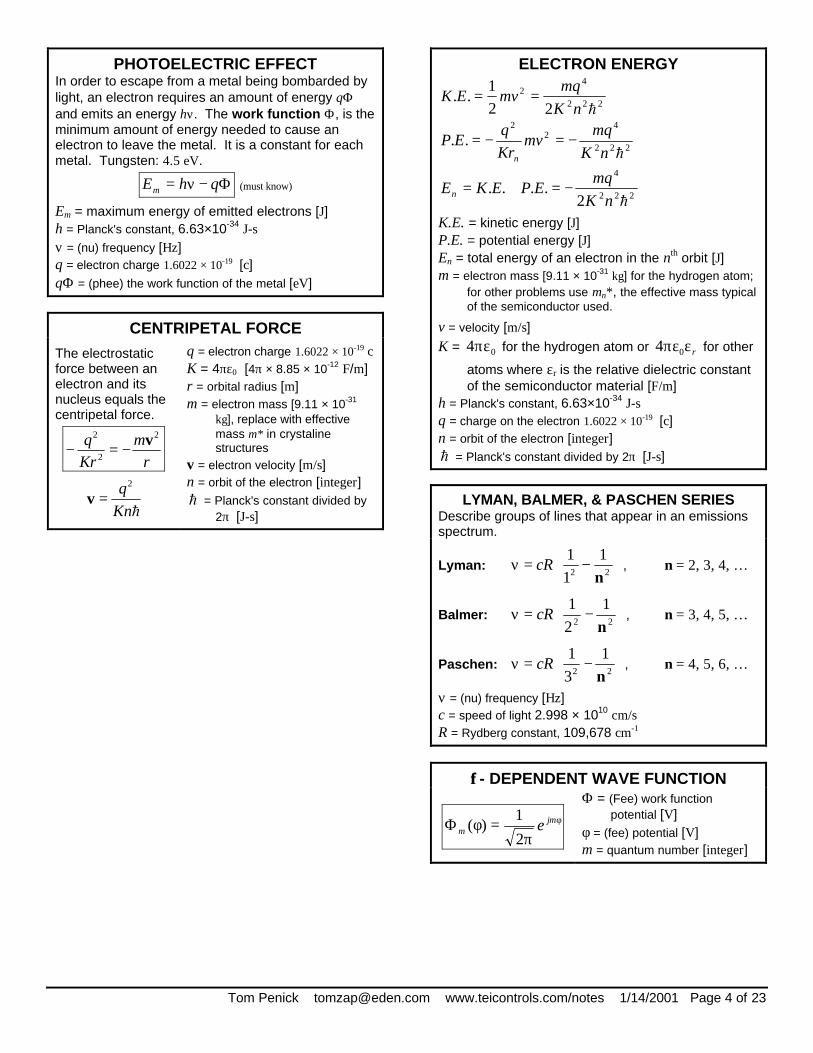
PHOTOELECTRIC EFFECT In order to escape from a metal being bombarded by light, an electron requires an amount of energy qΦ and emits an energy hν. The work function Φ, is the minimum amount of energy needed to cause an electron to leave the metal. It is a constant for each metal. Tungsten: 4.5 eV.
Φ−ν= qhEm (must know)
Em = maximum energy of emitted electrons [J] h = Planck's constant, 6.63×10⁻³⁴ J-s ν = (nu) frequency [Hz] q = electron charge 1.6022 × 10⁻¹⁹ [c] qΦ = (phee) the work function of the metal [eV]
CENTRIPETAL FORCE
The electrostatic force between an electron and its nucleus equals the centripetal force.
rm
Krq 2
2
2 v−=−
2qKn
=v h
q = electron charge 1.6022 × 10⁻¹⁹ c K = 4πε0 [4π × 8.85 × 10-12 F/m] r = orbital radius [m] m = electron mass [9.11 × 10⁻³¹
kg], replace with effective mass m* in crystaline structures
v = electron velocity [m/s] n = orbit of the electron [integer] h = Planck's constant divided by
2π [J-s]
ELECTRON ENERGY
222
42
22
1.. hnK
mqmvEK ==
222
42
2
.. hnKmq
mvKrq
EPn
−=−=
222
4
2.... hnK
mqEPEKEn −=+=
K.E. = kinetic energy [J] P.E. = potential energy [J] En = total energy of an electron in the nth orbit [J] m = electron mass [9.11 × 10⁻³¹ kg] for the hydrogen atom;
for other problems use mn*, the effective mass typical of the semiconductor used.
v = velocity [m/s]
K = 04πε for the hydrogen atom or rεπε04 for other
atoms where εr is the relative dielectric constant of the semiconductor material [F/m]
h = Planck's constant, 6.63×10⁻³⁴ J-s q = charge on the electron 1.6022 × 10⁻¹⁹ [c] n = orbit of the electron [integer] h = Planck's constant divided by 2π [J-s]
LYMAN, BALMER, & PASCHEN SERIES Describe groups of lines that appear in an emissions spectrum.
Lyman:
−=ν
22
1
1
1
ncR , n = 2, 3, 4, …
Balmer:
−=ν
22
1
2
1
ncR , n = 3, 4, 5, …
Paschen:
−=ν
22
1
3
1
ncR , n = 4, 5, 6, …
ν = (nu) frequency [Hz] c = speed of light 2.998 × 1010 cm/s R = Rydberg constant, 109,678 cm-1
φφ- DEPENDENT WAVE FUNCTION
φ
π=φΦ jm
m e2
1)(
Φ = (Fee) work function potential [V]
φ = (fee) potential [V] m = quantum number [integer]

Tom Penick [email protected] www.teicontrols.com/notes 1/14/2001 Page 5 of 23
BOHR MODEL Niels Bohr constructed a model for the hydrogen atom based on the mathematics of planetary systems. He made the following postulates:
1. Electrons exist in certain stable, circular orbits about the nucleus.
2. The electron may shift to an orbit of higher or lower energy, gaining or losing an amount of energy equal to the difference in energy levels by absorbing or emitting 1 photon of energy hν.
3. The angular momentum ρρθθ of the electron in an orbit is always an integral multiple of Planck's
constant divided by 2π. 0 / 2Nh Nρ = π = h .
BOHR ELECTRON ORBIT RADIUS The electron of the hydrogen atom may occupy one of several orbits n of radius r.
2 2 20* 4 rrm q = πε ε n h
r = orbit radius [m] m* = effective mass of the semiconductor material [kg] q = electron charge 1.6022 × 10⁻¹⁹ [C] ε0 = permittivity of free space [F/m]
εr = relative permittivity of the material [constant] n = orbit, n = 1 is ground state [integer] h = Planck's constant divided by 2π [J-s]
εεr RELATIVE PERMITTIVITY The ratio of the permittivity of the material to the permittivity of free space (ε0 = 8.85 × 10⁻¹² F/m). The permittivity of the material is then ε0εr. The relative permittivities of some common materials are:
Si 11.8, Ge 16, GaAs 13.2
SCHRÖDINGER WAVE EQUATION
In three dimensions: tj
Vm ∂
Ψ∂−=Ψ+Ψ∇−
hh 22
2
where 2
2
2
2
2
22
zyx ∂Ψ∂
+∂
Ψ∂+
∂Ψ∂
=Ψ∇
h = Planck's constant divided by 2π [J-s] m = quantum number [integer] ∇ = total energy of an electron in the nth orbit [J]
Ψ(x) = the wave function, having space and time dependencies
j = 1− t = time [s] x,y,z = position coordinates [m]
refer to WaveEquation.pdf for more information
EFFECTIVE MASS OF AN ELECTRON The effective mass of an electron is simply an adjustment to the standard electron mass that accounts for the influence of the lattice structure. This enables the same formulas to work for different elements.
22
2
/*
kdEdm
h=
m* = effective mass of an electron (n), hole (p). [kg]
h = Planck's constant divided by 2π [J-s]
d = derivative E = electron energy scale [J] k = wave vector [m-1]
The effective mass for several semiconductors is given below in terms of the free electron rest mass m0. These are average values appropriate for density of states calculations only.
Ge Si GaAs mn
* 0.55m0 1.1m0 0.067m0
mp* 0.37m0 0.56m0 0.48m0
E DONOR BINDING ENERGY The amount of energy required to excite a donor electron to the conduction band.
( )
4
2 20
*
8 r
m qE
h=
ε ε
E = donor binding energy [J] m* = effective mass of the
semiconductor material [kg] q = electron charge 1.60 × 10⁻¹⁹ [C] ε0 = permittivity of free space [F/m]
εr = relative permittivity of the material [constant]
h = Planck's constant, 6.63×10⁻³⁴ J-s
Tom Penick [email protected] www.teicontrols.com/notes 1/14/2001 Page 6 of 23
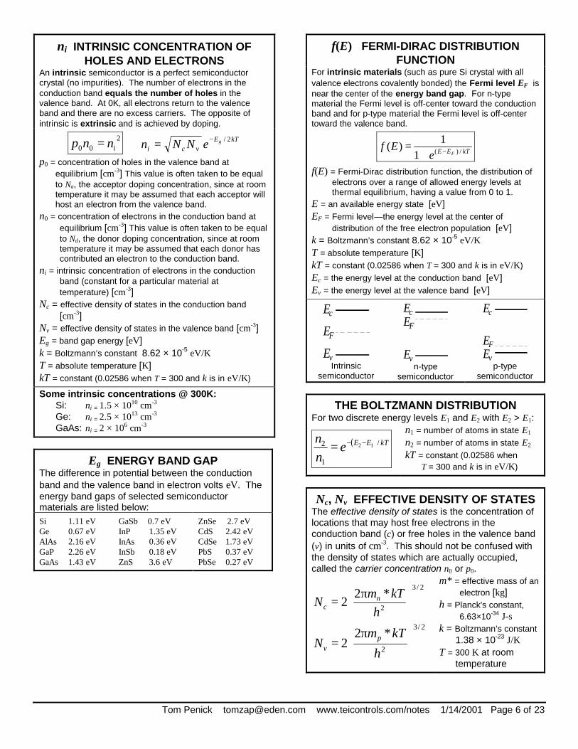
ni INTRINSIC CONCENTRATION OF HOLES AND ELECTRONS
An intrinsic semiconductor is a perfect semiconductor crystal (no impurities). The number of electrons in the conduction band equals the number of holes in the valence band. At 0K, all electrons return to the valence band and there are no excess carriers. The opposite of intrinsic is extrinsic and is achieved by doping.
200 innp =
kTEvci
geNNn 2/−=
p0 = concentration of holes in the valence band at equilibrium [cm-3] This value is often taken to be equal to Na, the acceptor doping concentration, since at room temperature it may be assumed that each acceptor will host an electron from the valence band.
n0 = concentration of electrons in the conduction band at equilibrium [cm-3] This value is often taken to be equal to Nd, the donor doping concentration, since at room temperature it may be assumed that each donor has contributed an electron to the conduction band.
ni = intrinsic concentration of electrons in the conduction band (constant for a particular material at temperature) [cm-3]
Nc = effective density of states in the conduction band [cm-3]
Nv = effective density of states in the valence band [cm-3] Eg = band gap energy [eV] k = Boltzmann’s constant 8.62 × 10⁻⁵ eV/K T = absolute temperature [K] kT = constant (0.02586 when T = 300 and k is in eV/K)
Some intrinsic concentrations @ 300K: Si: ni = 1.5 × 1010 cm-3 Ge: ni = 2.5 × 1013 cm-3 GaAs: ni = 2 × 106 cm-3
Eg ENERGY BAND GAP The difference in potential between the conduction band and the valence band in electron volts eV. The energy band gaps of selected semiconductor materials are listed below:
Si 1.11 eV Ge 0.67 eV AlAs 2.16 eV GaP 2.26 eV GaAs 1.43 eV
GaSb 0.7 eV InP 1.35 eV InAs 0.36 eV InSb 0.18 eV ZnS 3.6 eV
ZnSe 2.7 eV CdS 2.42 eV CdSe 1.73 eV PbS 0.37 eV PbSe 0.27 eV
f(E) FERMI-DIRAC DISTRIBUTION FUNCTION
For intrinsic materials (such as pure Si crystal with all valence electrons covalently bonded) the Fermi level EF is near the center of the energy band gap. For n-type material the Fermi level is off-center toward the conduction band and for p-type material the Fermi level is off-center toward the valence band.
kTEE FeEf /)(1
1)( −+
=
f(E) = Fermi-Dirac distribution function, the distribution of electrons over a range of allowed energy levels at thermal equilibrium, having a value from 0 to 1.
E = an available energy state [eV] EF = Fermi level—the energy level at the center of
distribution of the free electron population [eV] k = Boltzmann’s constant 8.62 × 10⁻⁵ eV/K T = absolute temperature [K] kT = constant (0.02586 when T = 300 and k is in eV/K)
Ec = the energy level at the conduction band [eV] Ev = the energy level at the valence band [eV]
FE
Ec
Ev Intrinsic
semiconductor
Ev
EcEF
n-type
semiconductor
Ec
Ev
EF
p-type
semiconductor
THE BOLTZMANN DISTRIBUTION For two discrete energy levels E1 and E2 with E2 > E1:
( ) kTEEenn /
1
2 12 −−=
n1 = number of atoms in state E1 n2 = number of atoms in state E2 kT = constant (0.02586 when
T = 300 and k is in eV/K)
Nc, Nv EFFECTIVE DENSITY OF STATES The effective density of states is the concentration of locations that may host free electrons in the conduction band (c) or free holes in the valence band (v) in units of cm-3. This should not be confused with the density of states which are actually occupied, called the carrier concentration n0 or p0.
2/3
2
*22
π
=h
kTmN n
c
2/3
2
*22
π=
h
kTmN p
v
m* = effective mass of an electron [kg]
h = Planck's constant, 6.63×10⁻³⁴ J-s
k = Boltzmann’s constant 1.38 × 10⁻²³ J/K
T = 300 K at room temperature
Tom Penick [email protected] www.teicontrols.com/notes 1/14/2001 Page 7 of 23
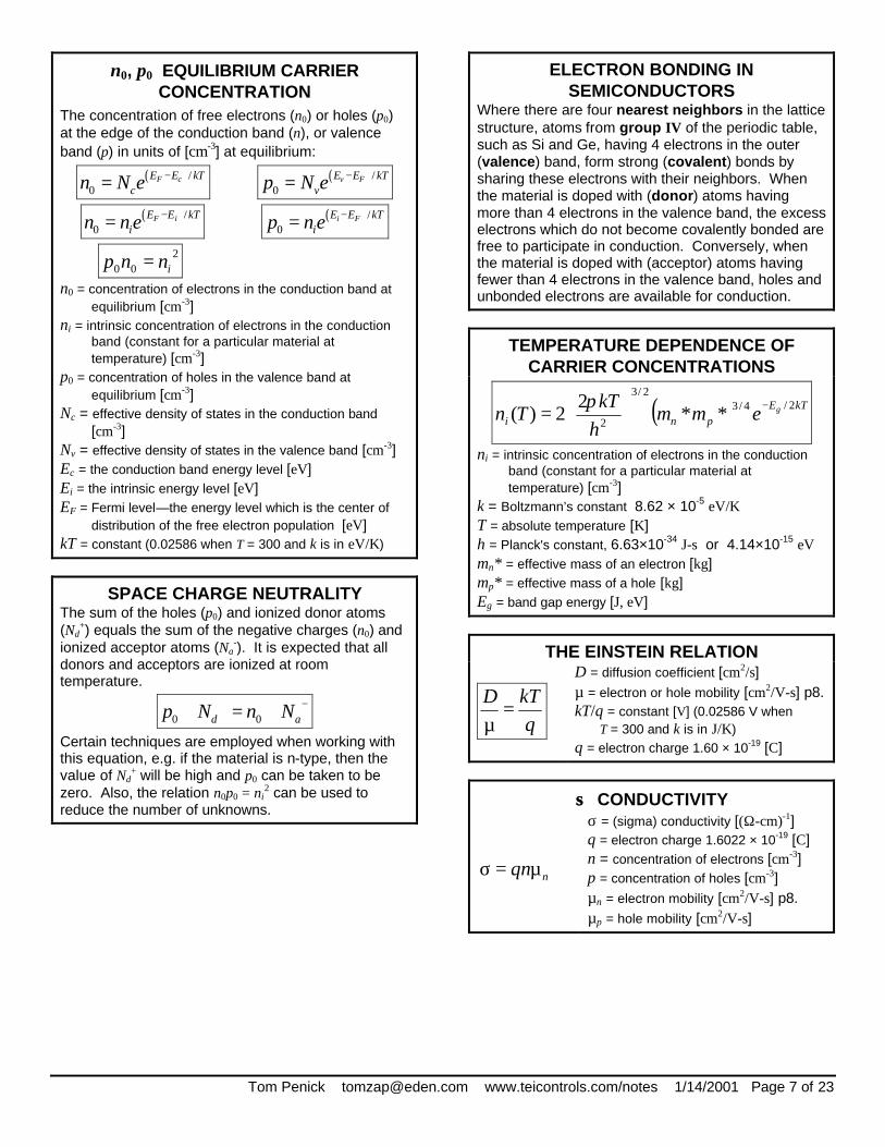
n0, p0 EQUILIBRIUM CARRIER CONCENTRATION
The concentration of free electrons (n0) or holes (p0) at the edge of the conduction band (n), or valence band (p) in units of [cm-3] at equilibrium:
( ) /0
F cE E kTcn N e −=
( ) /0
v FE E kTvp N e −=
( ) /0
F iE E kTin n e −=
( ) /0
i FE E kTip n e −=
2
00 innp =
n0 = concentration of electrons in the conduction band at equilibrium [cm-3]
ni = intrinsic concentration of electrons in the conduction band (constant for a particular material at temperature) [cm-3]
p0 = concentration of holes in the valence band at equilibrium [cm-3]
Nc = effective density of states in the conduction band [cm-3]
Nv = effective density of states in the valence band [cm-3] Ec = the conduction band energy level [eV] Ei = the intrinsic energy level [eV] EF = Fermi level—the energy level which is the center of
distribution of the free electron population [eV] kT = constant (0.02586 when T = 300 and k is in eV/K)
SPACE CHARGE NEUTRALITY The sum of the holes (p0) and ionized donor atoms (Nd
+) equals the sum of the negative charges (n0) and ionized acceptor atoms (Na
-). It is expected that all donors and acceptors are ionized at room temperature.
0 0d ap N n N+ −+ = +
Certain techniques are employed when working with this equation, e.g. if the material is n-type, then the value of Nd
+ will be high and p0 can be taken to be zero. Also, the relation n0p0 = ni
2 can be used to reduce the number of unknowns.
ELECTRON BONDING IN SEMICONDUCTORS
Where there are four nearest neighbors in the lattice structure, atoms from group IV of the periodic table, such as Si and Ge, having 4 electrons in the outer (valence) band, form strong (covalent) bonds by sharing these electrons with their neighbors. When the material is doped with (donor) atoms having more than 4 electrons in the valence band, the excess electrons which do not become covalently bonded are free to participate in conduction. Conversely, when the material is doped with (acceptor) atoms having fewer than 4 electrons in the valence band, holes and unbonded electrons are available for conduction.
TEMPERATURE DEPENDENCE OF CARRIER CONCENTRATIONS
( ) kTEpni
gemmhkT
Tn 2/4/32/3
2**
22)( −
=
π
ni = intrinsic concentration of electrons in the conduction band (constant for a particular material at temperature) [cm-3]
k = Boltzmann’s constant 8.62 × 10⁻⁵ eV/K T = absolute temperature [K] h = Planck's constant, 6.63×10⁻³⁴ J-s or 4.14×10⁻¹⁵ eV mn* = effective mass of an electron [kg] mp* = effective mass of a hole [kg] Eg = band gap energy [J, eV]
THE EINSTEIN RELATION
qkTD
=µ
D = diffusion coefficient [cm2/s] µ = electron or hole mobility [cm2/V-s] p8. kT/q = constant [V] (0.02586 V when
T = 300 and k is in J/K) q = electron charge 1.60 × 10⁻¹⁹ [C]
σσ CONDUCTIVITY
nqnµ=σ
σ = (sigma) conductivity [(Ω-cm)-1] q = electron charge 1.6022 × 10⁻¹⁹ [C] n = concentration of electrons [cm-3] p = concentration of holes [cm-3] µn = electron mobility [cm2/V-s] p8. µp = hole mobility [cm2/V-s]

Tom Penick [email protected] www.teicontrols.com/notes 1/14/2001 Page 8 of 23
µµn ELECTRON MOBILITY AND DRIFT Electron mobility is the ease with which electrons drift in the material, or the average particle drift velocity per unit of electric field (cm/s/V/cm → cm2/V-s). There is an upper limit to the velocity, called saturation velocity vs, that is caused by scattering, about 107 cm/s for silicon. See EINSTEIN RELATION p7.
*x
nn x
qtm
µ = =v
E
q = electron charge 1.6022 × 10⁻¹⁹ [C] µn = electron mobility [cm2/V-s] µp = hole mobility [cm2/V-s] Ex = electric field applied in the x-direction [V/cm]
xv = average particle drift velocity [cm/s]
µµn [cm2/V-s] µµp [cm2/V-s]
Silicon Si 1350 480
Germanium Ge 3900 1900
Gallium Arsenide GaAs 8500 400
J CURRENT DENSITY
( )x n p x xJ q n p= µ + µ = σE E
If an electric field is present in addition to the carrier gradient, the current densities will each have a drift component and a diffusion component:
driftdiffusion
( )( ) ( ) ( )
( )( ) ( ) ( )
n n n
p p p
dn xJ x q n x x qD
dx
dp xJ x q p x x qD
dx
= µ +
= µ −
1442443 14243647486447448
E
E
Jn, Jp = current density due to electrons, holes [A/cm2] q = electron charge 1.6022 × 10⁻¹⁹ [C] n, p = concentration of electrons, holes [cm-3] µn, µp = electron mobility, hole mobility [cm2/V-s] p8. Ex = electric field in the x-direction [V/cm] Dn, Dp = diffusion coefficient for electrons, holes [cm2/s] σ = (sigma) conductivity [(Ω-cm)-1]
INTENSITY OF LIGHT TRANSMITTED THROUGH A SEMICONDUCTOR
lt eII α−= 0
It = intensity of transmitted light [watts or photons/cm2-s]
I0 = light source intensity [watts or photons/cm2-s]
α = absorption coefficient [cm-1] l = sample thickness [cm]
DRIFT AND DIFFUSION CURRENTS The two basic processes of current conduction are diffusion due to a carrier gradient, and drift in an electric field. Charge carriers (electrons or holes) move by diffusion from areas of high carrier concentration to areas of low carrier concentration. Since the amount of current is proportional to the carrier gradient rather than the number of carriers, minority carriers may contribute significantly to the diffusion current. The recombination of electrons and holes as carriers pass through a material can create a carrier gradient and produce diffusion current. Drift current is the result of electrons in random motion being influenced by an electric field. Although electrons are moving in many directions, the net movement will be against the electric field, holes move with the field. The result is current flow with the electric field. Drift current flows in response to an applied voltage.
EE(x) ELECTRIC FIELD The electric field E(x) is equal to the change in voltage in the x-direction. An electric field occurs when there is a gradient in the doping concentration, and is related to the change in the intrinsic energy level of the semiconductor material. The direction of an electric field is uphill in a band diagram. Electrons drift down the slope, while holes drift in the field direction.
An electric field may also be the result of a semiconductor junction, see page 11.
( ) 1( ) idEdV xx
dx q dx= − =E
( )( )
( )1p
p
D dp xx
p x dx=
µE
E(x)
v
Ei
E
Ec
E(x) = electric field as a function of location [V/cm] V = voltage [V] q = electron charge 1.6022 × 10⁻¹⁹ [C] Ei = the intrinsic energy level [eV] Dp = diffusion coefficient for holes [cm2/s] µp = hole mobility [cm2/V-s] p8. P(x) = distribution of holes [cm-3]
Tom Penick [email protected] www.teicontrols.com/notes 1/14/2001 Page 9 of 23
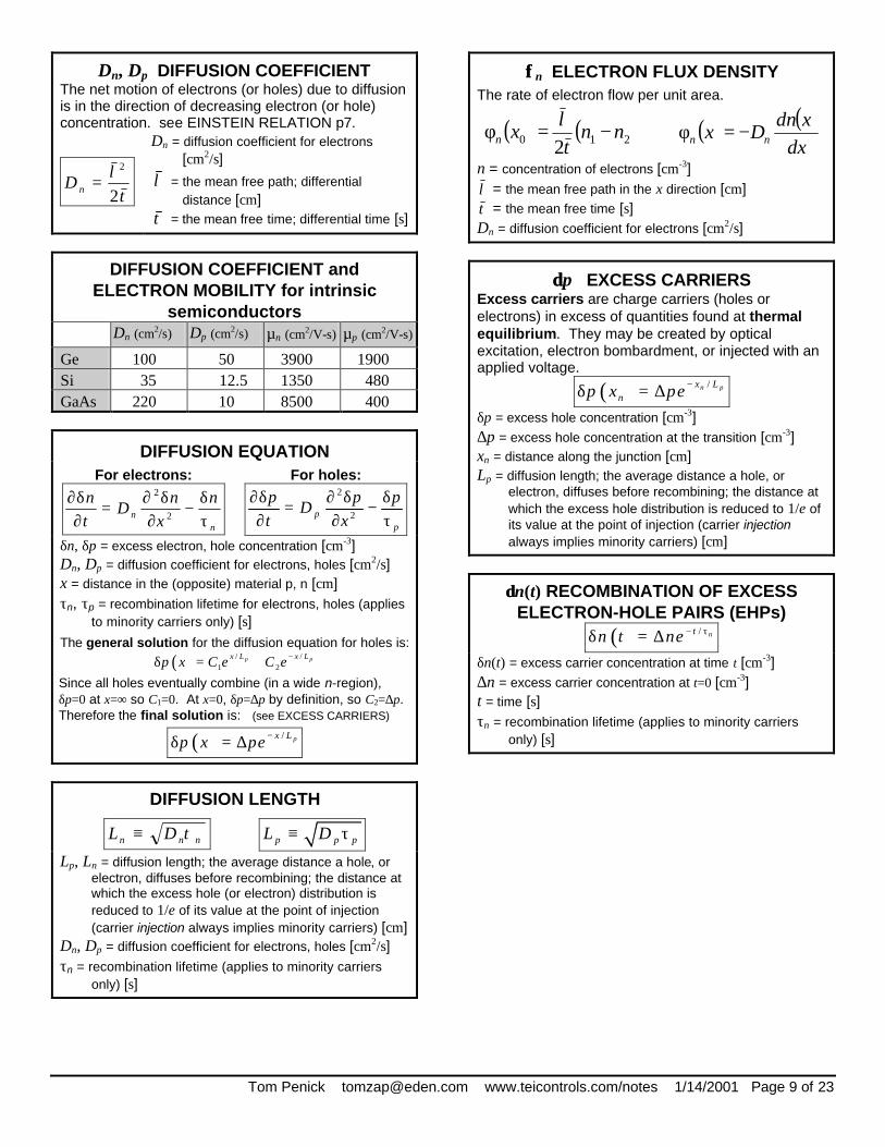
Dn, Dp DIFFUSION COEFFICIENT The net motion of electrons (or holes) due to diffusion is in the direction of decreasing electron (or hole) concentration. see EINSTEIN RELATION p7.
tl
D n 2
2
=
Dn = diffusion coefficient for electrons [cm2/s]
l = the mean free path; differential distance [cm]
t = the mean free time; differential time [s]
DIFFUSION COEFFICIENT and ELECTRON MOBILITY for intrinsic
semiconductors Dn (cm2/s) Dp (cm2/s) µn (cm2/V-s) µp (cm2/V-s)
Ge 100 50 3900 1900 Si 35 12.5 1350 480 GaAs 220 10 8500 400
DIFFUSION EQUATION
For electrons:
nn
nx
nD
tn
τδ
−∂
δ∂=
∂δ∂
2
2
For holes: 2
2pp
p p pD
t x∂δ ∂ δ δ
= −∂ ∂ τ
δn, δp = excess electron, hole concentration [cm-3] Dn, Dp = diffusion coefficient for electrons, holes [cm2/s] x = distance in the (opposite) material p, n [cm] τn, τp = recombination lifetime for electrons, holes (applies
to minority carriers only) [s]
The general solution for the diffusion equation for holes is:
( ) / /1 2
p px L x Lp x C e C e −δ = +
Since all holes eventually combine (in a wide n-region), δp=0 at x=∞ so C1=0. At x=0, δp=∆p by definition, so C2=∆p. Therefore the final solution is: (see EXCESS CARRIERS)
( ) / px Lp x pe −δ = ∆
DIFFUSION LENGTH
nnn DL τ≡ p p pL D≡ τ
Lp, Ln = diffusion length; the average distance a hole, or electron, diffuses before recombining; the distance at which the excess hole (or electron) distribution is reduced to 1/e of its value at the point of injection (carrier injection always implies minority carriers) [cm]
Dn, Dp = diffusion coefficient for electrons, holes [cm2/s] τn = recombination lifetime (applies to minority carriers
only) [s]
φφn ELECTRON FLUX DENSITY The rate of electron flow per unit area.
( ) ( )210 2nn
tl
xn −=φ ( ) ( )dx
xdnDx nn −=φ
n = concentration of electrons [cm-3]
l = the mean free path in the x direction [cm] t = the mean free time [s] Dn = diffusion coefficient for electrons [cm2/s]
δδp EXCESS CARRIERS Excess carriers are charge carriers (holes or electrons) in excess of quantities found at thermal equilibrium. They may be created by optical excitation, electron bombardment, or injected with an applied voltage.
( ) /n px Lnp x pe −δ = ∆
δp = excess hole concentration [cm-3] ∆p = excess hole concentration at the transition [cm-3] xn = distance along the junction [cm] Lp = diffusion length; the average distance a hole, or
electron, diffuses before recombining; the distance at which the excess hole distribution is reduced to 1/e of its value at the point of injection (carrier injection always implies minority carriers) [cm]
δδn(t) RECOMBINATION OF EXCESS ELECTRON-HOLE PAIRS (EHPs)
( ) / ntn t ne − τδ = ∆
δn(t) = excess carrier concentration at time t [cm-3] ∆n = excess carrier concentration at t=0 [cm-3] t = time [s] τn = recombination lifetime (applies to minority carriers
only) [s]

Tom Penick [email protected] www.teicontrols.com/notes 1/14/2001 Page 10 of 23
V0 CONTACT POTENTIAL The difference in intrinsic energy levels in the p and n regions.
n
p
p
p
qkT
V ln0 = inip EEV −=0
pp, pn = equilibrium concentration of holes in the boundary region of the p material, of the n material [cm-3]. For the n material, this might just be the intrinsic concentration ni, unless there are also acceptors present. In the p material this could just be the acceptor concentration NA, assuming that the intrinsic concentration is small in comparison and there are no donor atoms that would give up electrons to the acceptors.
kT/q = constant (0.02586 when T = 300 and k is in J/K) (refer to pn JUNCTION section, page 10.)
p-n STEP JUNCTION For a step junction (an abrupt transition), the donors and acceptors give up all of their donor electrons and holes to the adjacent region so that pp = Na and nn = Nd. The effect of acceptor concentration in the p region is to bring the Fermi energy level close to the valence band, and the effect of donor concentration in the n region is to bring the Fermi level close to the conduction band. When the p and n regions are brought together, the Fermi levels must be equal at equilibrium. See Band Diagram below.
( ) kTEEip
Fpipenp /−=
( ) kTEEin
inFnenn /−=
kTqV
p
n
n
p enn
p
p /0==
pp = concentration of holes in the boundary region of the p material [cm-3]
nn = concentration of electrons in the boundary region of the n material [cm-3]
ni = intrinsic concentration of electrons [cm-3] Eip, Ein = intrinsic energy level in the p region, n region
[eV] EFp, EFn = Fermi energy level in the p region, n region [eV] kT = constant (0.02586 when T = 300 and k is in eV/K) Na = concentration of acceptors (atoms that may gain an
electron) [cm-3] Nd = concentration of donors (atoms that may lose an
electron) [cm-3] V0 = contact potential [eV]
EQUILIBRIUM BAND DIAGRAM In a p-n junction at equilibrium, the Fermi energy level of the p-material is equal to the Fermi energy level of the n-material. Refer to the relations under pn STEP JUNCTION and V0 CONTACT POTENTIAL above to calculate band gap values shown.
E
EF
vp
Eip
cp
E EF
Ein
Evn
qV0
Ecn
junc-tion
p-material n-material
Ecp = the p-material conduction band energy level [eV] Eip = the p-material intrinsic energy level [eV] EF = the Fermi energy level [eV] Evp = the p-material valence band energy level [eV] Ecn = the n-material conduction band energy level [eV] Ein = the n-material intrinsic energy level [eV] Evn = the n-material valence band energy level [eV]
W BOUNDARY WIDTH A p-n junction is shown with Nd > Na, hence the transition region (also called the depletion region) extends further into the p material.
W
-xp0
p- - - -- - - -- - - -- - - -
x xn00+ + + ++ + + ++ + + ++ + + +
n
2/1
22
2/1
0
2/1
0
11ln
2
1122
+
ε=
+
ε=
+ε=
dai
da
dada
da
NNn
NNqkT
NNqV
NNNN
qV
W
W = boundary width, width of the transition region [cm] ε = permittivity [F/cm]
Na = concentration of acceptors (atoms that may gain an electron) [cm-3]
Nd = concentration of donors (atoms that may lose an electron) [cm-3]
V0 = contact potential [eV] q = electron charge 1.60 × 10⁻¹⁹ [C]
Tom Penick [email protected] www.teicontrols.com/notes 1/14/2001 Page 11 of 23
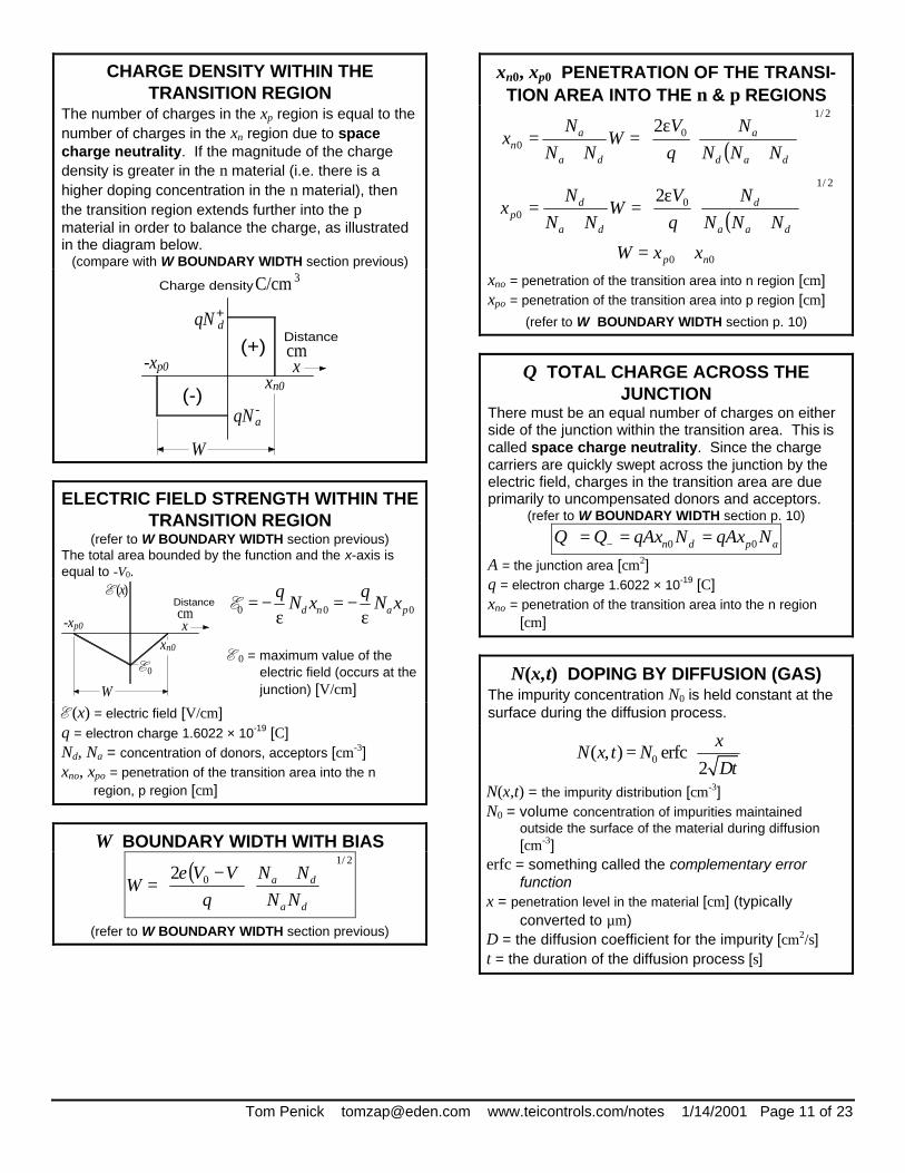
CHARGE DENSITY WITHIN THE TRANSITION REGION
The number of charges in the xp region is equal to the number of charges in the xn region due to space charge neutrality. If the magnitude of the charge density is greater in the n material (i.e. there is a higher doping concentration in the n material), then the transition region extends further into the p material in order to balance the charge, as illustrated in the diagram below.
(compare with W BOUNDARY WIDTH section previous)
Charge densityC/cm 3
+qN d
(-)
W
-xp0
qN -a
xxn0
(+)Distancecm
ELECTRIC FIELD STRENGTH WITHIN THE TRANSITION REGION
(refer to W BOUNDARY WIDTH section previous) The total area bounded by the function and the x-axis is equal to -V0.
W
p0-x
x( )EDistance cm
xn0
0E
x0 0 0d n a p
q qN x N x= − = −
ε εE
E0 = maximum value of the
electric field (occurs at the junction) [V/cm]
E(x) = electric field [V/cm] q = electron charge 1.6022 × 10⁻¹⁹ [C] Nd, Na = concentration of donors, acceptors [cm-3] xno, xpo = penetration of the transition area into the n
region, p region [cm]
W BOUNDARY WIDTH WITH BIAS
( )2/1
02
+−=
da
da
NN
NN
q
VVW
ε
(refer to W BOUNDARY WIDTH section previous)
xn0, xp0 PENETRATION OF THE TRANSI-TION AREA INTO THE n & p REGIONS
( )
2/1
00
2
+
ε=
+=
dad
a
da
an NNN
N
q
VW
NN
Nx
( )
2/1
00
2
+
ε=
+=
daa
d
da
dp NNN
N
q
VW
NN
Nx
00 np xxW +=
xno = penetration of the transition area into n region [cm] xpo = penetration of the transition area into p region [cm]
(refer to W BOUNDARY WIDTH section p. 10)
Q TOTAL CHARGE ACROSS THE JUNCTION
There must be an equal number of charges on either side of the junction within the transition area. This is called space charge neutrality. Since the charge carriers are quickly swept across the junction by the electric field, charges in the transition area are due primarily to uncompensated donors and acceptors.
(refer to W BOUNDARY WIDTH section p. 10)
apdn NqAxNqAxQQ 00 === −+
A = the junction area [cm2] q = electron charge 1.6022 × 10⁻¹⁹ [C] xno = penetration of the transition area into the n region
[cm]
N(x,t) DOPING BY DIFFUSION (GAS) The impurity concentration N0 is held constant at the surface during the diffusion process.
0( , ) erfc2
xN x t N
Dt
=
N(x,t) = the impurity distribution [cm-3] N0 = volume concentration of impurities maintained
outside the surface of the material during diffusion [cm-3]
erfc = something called the complementary error function
x = penetration level in the material [cm] (typically converted to µm)
D = the diffusion coefficient for the impurity [cm2/s] t = the duration of the diffusion process [s]
Tom Penick [email protected] www.teicontrols.com/notes 1/14/2001 Page 12 of 23
N(x,t) DOPING BY DIFFUSION LAYER A layer of impurities is applied to the surface before diffusion. No impurities escape from the material during the diffusion process.
( )2/2
( , )x DtsN
N x t eDt
−=
π
NS = area concentration of impurities in the surface layer [atoms/cm2]
see above for other variable definitions
I DIODE EQUATION
( ) ( )11 /0
/ −=−
+= kTqVkTqV
pn
nn
p
p eIenLD
pL
DqAI
and for the non-ideal diode: ( )1/0 −= nkTqVeII
I = diode current [A] q = electron charge 1.6022 × 10⁻¹⁹ [C] A = the junction area [cm2] Dp, Dn = diffusion coefficient for holes, electrons [cm2/s] Lp, Ln = diffusion length; the average distance a hole, or
electron, diffuses before recombining; the distance at which the excess hole (or electron) distribution is reduced to 1/e of its value at the point of injection (carrier injection always implies minority carriers) [cm]
pn = concentration of holes in the boundary region of the n material [cm-3]
np = concentration of electrons in the boundary region of the p material [cm-3]
kT = constant (0.02586 when T = 300 and k is in eV/K)
I0 = saturation current [A] n = ideality factor 0 < n < 1
I0 REVERSE SATURATION CURRENT
+= p
n
nn
p
p nL
Dp
L
DqAI0
C CAPACITANCE OF P-N JUNCTIONS There are basically two types of capacitance associated with a junction:
1. junction capacitance or transition region capacitance or depletion layer capacitance. This is the capacitance due to the dipole in the transition region (the area containing two oppositely charged regions merging at the junction). This type is dominant under reverse-bias conditions. Capacitance varies with voltage since the width of the transition region varies with voltage.
( )
1/2
02d a
jd a
N NA qC A
W V V N N
ε= = ε
ε − +
2. charge storage capacitance or diffusion capacitance. This is the capacitance due to the lagging behind of voltage as current changes. This type is dominant under forward-bias conditions. Charge storage capacitance can be a serious limitation in high frequency circuits involving forward-biased p-n junctions.
Stored charge: p p n pQ I qA p L= τ = ∆
/qV kTp nqAL p e=
Capacitance due to small changes in the stored charge, i.e. charge storage capacitance:
ps
dQC
dV=
2/qV kT
p n
qAL p e
kT=
p
qI
kT= τ
Cj JUNCTION CAPACITANCE The capacitance of an asymmetrically doped junction is determined by only one of the doping concentrations. Cj is a voltage-variable capacitance.
2/1
0
2
2
−
= dj NVV
qAC
ε
For a p+-n junction,
da NN << , Wxn ≈0
Cj = junction capacitance [F] A = the junction area [cm2] q = electron charge 1.6022 × 10⁻¹⁹ [C] ε = permittivity [F/cm] V0 = contact potential [eV] (V0 – V) = barrier height [eV] Nd = concentration of donors (atoms that may lose an
electron) [cm-3]
Tom Penick [email protected] www.teicontrols.com/notes 1/14/2001 Page 13 of 23
THE p+-n JUNCTION The p material is more heavily doped so that the depletion layer width W extends primarily into the n side.
n−∝ rj VC for 0VVr >>
( ) mGxxN d = )2/(1 += mn
da NN << ,
Wxn ≈0
Cj = junction capacitance [F] n = doping gradient factor
n = 1/3 for a linearly graded junction n = 1/2 for an abrupt junction n > 1/2 for a hyperabrupt junction n = 2 for a varacter device
G = a constant Vr = V0 = contact potential [eV] Nd = concentration of donors (atoms that may lose an
electron) [cm-3]
DIRECT RECOMBINATION The direct recombination of electron and hole pairs occurs when electrons fall from the conduction band to empty holes in the valence band. Light is produced. The net rate of change in the conduction band electron concentration is the thermal generation rate minus the recombination rate:
( ) ( ) ( )tptnndt
tdnrir α−α= 2
αr = constant of recombination proportionality [cm-3] ni = intrinsic concentration of electrons in the conduction
band [cm-3] n = concentration of electrons [cm-3] p = concentration of holes [cm-3]
If excess carrier concentrations are small and the material is extrinsic, we can say:
( ) ( )tnpdt
tndr δα−=
δ0 ,
where ( ) nr ttp nenetn τ−α− ∆=∆=δ /0
and ( ) ( ) 10
00
1 −α≈+α
=τ ppn r
rn
δn(t) = concentration of excess electrons [cm-3] ∆n = concentration of excess electrons at t = 0 [cm-3] τn = recombination lifetime, i.e. the average time an
electron spends in the energy band before recombination [s]
The excess majority carriers decay at the same rate as the minority carriers, so τn = τp. If ∆p = ∆n, then δp(t) = δn(t).
INDIRECT RECOMBINATION, TRAPPING The majority of recombination events in indirect materials, such as column IV semiconductors, occur via recombination levels within the band gap. These energy levels are called trapping centers and may be denoted by Er. The process of recombination through incremental steps through the energy band is called indirect recombination. The energy loss due to recombination of electron/hole pairs is given up mostly as heat (rather than light). The process of indirect recombination is more complex than direct recombination since carriers that have shifted to a trapping energy level may return to their original energy level without recombining. The rate of recombination may be measured by monitoring the conductivity of a sample.
( ) ( ) ( ) ][ pn tptnqt µ+µ=σ
σ = (sigma) conductivity [(Ω-cm)-1] q = electron charge 1.6022 × 10⁻¹⁹ [C] n = concentration of electrons [cm-3] p = concentration of holes [cm-3] µn = electron mobility [cm2/V-s] p8. µp = hole mobility [cm2/V-s]
STEADY STATE ELECTRON AND HOLE CONCENTRATION
The steady state condition is when the rate of generation of electron hole pairs equals the recombination rate.
( )
( ) kTFEi
kTEFi
pi
in
enp
enn/
/
−
−
=
=
nopgpn τ=δ=δ
n = concentration of electrons [cm-3]
p = concentration of holes [cm-3] ni = intrinsic concentration of
electrons in the conduction band [cm-3]
Ei = intrinsic energy level [J, eV] Fn, Fp = quasi Fermi energy level
for electrons, holes [J, eV] δn, δp = excess carrier
concentration [cm-3] gop = optical electron hole pair
generation rate [cm-3-s-1] τn = recombination lifetime (applies
to minority carriers only) [s]

Tom Penick [email protected] www.teicontrols.com/notes 1/14/2001 Page 14 of 23
ΦΦB POTENTIAL BARRIER HEIGHT The Schottky potential barrier height for electron injection from the metal into the semiconductor conduction band is
χ−Φ=Φ qqq mB
qΦB = potential barrier height [eV]
qΦm = metal work function [eV] qχ = electron affinity [eV]
punch through – An occurrence of breakdown below
the expected breakdown voltage caused by the transition region extending across the entire width of the layer. This can be a problem in short, lightly-doped regions.
avalanche breakdown – A high-energy electron is driven from the p-region into the transition region by an externally applied voltage. It collides with the lattice, creating an electron-hole pair. The two electrons are swept toward the n-region while the hole is swept toward the p-region under rapid acceleration due to a strong electric field. With sufficient energy, these particles participate in additional lattice collisions within the transition region, causing the creation of additional electron-hole pairs. High reverse-bias voltage and high n-region doping concentrations contribute to the effect, but the zener (tunneling) effect takes over at very high doping concentrations.
Zener effect – The n- and p-regions of an abrupt p-n junction must both be heavily doped. The junction is reversed-biased to the extent that the energy bands cross, that is, the energy level of the n-material conduction band is below that of the p-material valence band. These conditions permit electrons to tunnel from Evp to Ecn and current flows from n to p as illustrated in the lower diagram at right.
Note that the materials in the diagram at right is degenerate type material, meaning that the doping concentration is so high that the Fermi level lies within the valence band of the p-material and within the conduction band of the n-type material.
.
DIODES
Tunnel diode – The tunnel diode operates (in certain regions of its I-V characteristic) by the quantum mechanical tunneling of electrons through the potential barrier of the junction. For reverse current, this is essentially the zener effect but requires only a small reverse bias. Applications include high-speed switching and logic circuits.
Photo diodes, solar cells – The junction is operated in the fourth quadrant of its I-V characteristic. The voltage produced is restricted to values less than the contact potential, typically less than 1V. Many compromises are made in solar cell design.
Junction depth in the n material must be less than Lp to allow holes generated near the survace to diffuse to the junction before they recombine.
Many surface contact traces are required to collect current from this thin layer due to its high resistance. But these traces block incoming light.
In order to have a high contact potential V0, heaving doping is required.
To have long lifetimes, doping must be reduced.
Solar cells are expensive to fabricate and produce only modest amounts of power.
Sunlight may be concentrated to increase output but efficiency is lost. GaAs and related compounds can be used at the higher temperatures.
Photo diodes, photodetectors – The junction is operated in the third quadrant of its I-V characteristic. In this region, current is essentially independent of voltage but proportional to the optical generation rate, making the device useful in measuring illumination levels or converting time-varying optical signals into electrical signals. It is usually desirable for these devices to act quickly, so the transition region W is made large. When an EHP is generated in this region, the electric field quickly sweeps the electron to the n side and the hole to the p side.
Varactor diode – This device employs the voltage-variable capacitance characteristic of a reverse-biased p-n junction. In a graded junction, the relationship between capacitance and voltage is
nrj VC −∝ for 0VVr >>
For a linearly graded junction, the value of n is ½. The value increases with more abrupt junctions.
Zener diode – The zener diode is a breakdown diode designed to break down abruptly at a particular voltage. Although named for the zener or tunneling breakdown mechanism, the avalanche effect is actually the more commonly used breakdown mechanism in zener diodes. A common application is voltage regulator.
p-material
Ecp
junc-tion
n-material
e-Evp
EFp
vnE
Ecn
EFn
Ecp
Evp
EFp
vnE
Ecn
EFne-
Tunneling with forward bias (top) and reverse bias (bottom)
Tom Penick [email protected] www.teicontrols.com/notes 1/14/2001 Page 15 of 23
BJTs
THE p+-n-p TRANSISTOR The emitter (p+) is more heavily doped so that the depletion region extends primarily into the base region.
p2
3
collector
5
+
emitter
p
1
nbase
4
(1) injected holes lost to recombination in the base (2) holes that fail to be recombined in the base are swept
across the reverse-biased collector junction by the electric field
(3) thermally generated electrons and holes are swept across the CB junction by the electric field make up the reverse saturation current of the collector junction
(4) electrons supplied by the base contact recombine with holes from (1), hence (1) and (4) are equal in magnitude
(5) electrons injected across the forward-biased emitter junction; this current is small due to the heavily doped emitter
For a n-p-n transistor, simply reverse the roles of electrons and holes.
NORMAL BIASING IN THE p+-n-p TRANSISTOR
Normal biasing in the p-n-p transistor means that the emitter-base junction is forward-biased and the collector-base junction is reverse-biased. Normal biasing results in reduced width of the emitter-base transition region and increased widthof the collector-base transition region.
bp∆ E ∆pC
Iemitter
+p
E
+
forward bias
I
n
W
base
p
C
collector
reverse biasIB
+
( )/ 1EBqV kTE np p e∆ = − , ( )/ 1CBqV kT
C np p e∆ = −
∆pE, ∆pC = excess hole concentration at the edge of the
emitter (∆pE) and collector (∆pC) depletion regions [cm-3]
VEB, VCB = emitter to base voltage, normally positive (VEB), collector to base voltage, normally negative (VCB) [V]
Wb = the width of the neutral base region; very important to the speed and efficiency of the transistor; this region is short so that most of the injected holes pass through to the collector (assisted by the electric field at the CB junction) without recombining in the base. [cm]
ENERGY BAND DIAGRAMS FOR THE p+-n-p TRANSISTOR
at equilibrium
collectoremitter base
FEEv
Ec
p+
qV0EB
n p
normal bias
V )BC+(q V0BC
base
FEEv
emitter
Ec
-VEB)(q V0EB
p+
collector
pn
FE

Tom Penick [email protected] www.teicontrols.com/notes 1/14/2001 Page 16 of 23
THE DIFFUSION EQUATION AND THE p+-n-p TRANSISTOR
Refer to the previous drawing.
The diffusion equation: ( ) ( )2
2 2n n
n p
d p x p x
dx L
δ δ=
The diffusion equation solution: ( ) / /
1 2n p n px L x L
np x C e C e−δ = +
Boundary conditions:
( ) 1 20n Ep x C C pδ = = + = ∆
( ) / /1 2
b p b pW L W Ln bp x W C e C e−δ = = +
Solving for C1 and C2: /
1 / /
b p
b p b p
W LC E
W L W L
p p eC
e e
−
−
∆ − ∆=
−
/
2 / /
b p
b p b p
W LE C
W L W L
p e pC
e e−
∆ − ∆=
−
∆pE, ∆pC = excess hole concentration at the edge of the
emitter (∆pE) and collector (∆pC) depletion regions [cm-3]
Wb = the width of the base region not taken up by transition regions [cm]
Lp = diffusion length; the average distance a hole diffuses before recombining [cm]
∆∆p DIFFUSION IN THE BASE REGION The following is applicable to a p-n-p transistor; these values are used in other equations. The ∆ symbol usually indicates a difference between two values; in this case it would be the difference between the total number of holes and those not available for conduction, two values in which we are not interested. ∆∆pE = excess hole concentration at the boundary of the
emitter-base depletion region [cm-3] ∆∆pC = excess hole concentration at the boundary of the
collector-base depletion region (∆pC = -pn when the collector is strongly reverse-biased) [cm-3]
( )/ 1EBqV kTE np p e∆ = − ( )/ 1CBqV kT
C np p e∆ = −
pn = concentration of excess holes in the base region [cm-3] q = electron charge 1.6022 × 10⁻¹⁹ [C] VEB = emitter-to-base voltage [V] VCB = collector-to-base voltage [V]
IE, IC, IB TRANSISTOR CURRENTS Note: ctnh is 1/tanh, csch is 1/sinh.
ctnh cschp b bEp E C
p p p
D W WI qA p p
L L L
= ∆ − ∆
csch ctnhp b bC E C
p p p
D W WI qA p p
L L L
= ∆ − ∆
tanh2
p bB E C
p p
D WI qA p p
L L
= ∆ + ∆
IEp = the hole component of the emitter current [A] IC = collector current [A] IB = base current [A] q = electron charge 1.6022 × 10⁻¹⁹ [C] A = cross-sectional junction area (uniform for both
junctions) [cm2] Dp = diffusion coefficient for holes [cm2/s] Lp = diffusion length; the average distance a hole diffuses
before recombining [cm] ∆pE = concentration of excess holes at the boundary of the
emitter-base depletion region [cm-3] ( )/ 1EBqV kT
E np p e∆ = −
∆pC = concentration of excess holes at the boundary of the collector-base depletion region (∆pC = -pn when the collector is strongly reverse-biased) [cm-3]
( )/ 1CBqV kTC np p e∆ = −
Wb = width of the base region [cm]
αα CURRENT TRANSFER RATIO The ratio of collector to emitter current, or common-base current gain. To make α close to 1, make the base narrow so not many holes recombine in the base.
C
E
II
α =1
Ep
En Ep
BIbB
a I Iβ
= = = γ =+ β +
a = (qADp/Lp) ctnh(Wb/Lp) b = (qADp/Lp) csch(Wb/Lp) B = ic/iEp = bpn, the base transport factor, the fraction of
injected holes that make it across the base to the collector
IEp = emitter current due to holes [A] IEn = emitter current due to electrons [A]
γ = emitter injection efficiency
Tom Penick [email protected] www.teicontrols.com/notes 1/14/2001 Page 17 of 23
ββ GAIN FACTOR The ratio of collector to base current, or base-to-collector current amplification factor, or common-emitter current gain.
( )1 1 1EpC
B En Ep
BII BI I B I B
γ αβ = = = =
+ − − γ − α
(see previous for description of variables)
γγ EMITTER INJECTION EFFICIENCY γ ≈ 1 is the emitter current due entirely to hole injection (carrier injection always implies minority carriers). To make γ as large as possible, make the emitter heavily doped. The superscripts indicate which side of the emitter-base junction is being referred to.
1 1
1 tanh 1n p n pp n n p n nbp n n p nn p p p n p p
Ep
Ep En
L n L nWL p L L p
I
I I
− − µ µ
γ = + ≈ + µ µ
=+
Lp, Ln = diffusion length; the average distance a hole, or electron, diffuses before recombining; the distance at which the excess hole (or electron) distribution is reduced to 1/e of its value at the point of injection [cm]
pp = concentration of holes in the boundary region of the p material [cm-3]
nn = concentration of electrons in the boundary region of the n material [cm-3]
Wb = base width in a BJT, measured between the edges of the emitter and collector junction depletion regions [cm]
µn = electron mobility [cm2/V-s] p8. µp = hole mobility [cm2/V-s]
IE, IC EBERS-MOLL EQUATIONS These equations for transistor current allow for asymmetry between the junctions.
( ) ( )( )
//
/
1 1
1
CBEB
EB
E EN EI
qV kTqV kTES I CS
qV kTI C EO
I I I
I e I e
I I e
= +
= − − α −
= α − −
(e1)
(e2)
(e3)
( ) ( )( )
//
/
1 1
1
CBEB
CB
C CN CI
qV kTqV kTN ES CS
qV kTN E CO
I I I
I e I e
I I e
= +
= α − − −
= α − −
(c1)
(c2)
(c3)
To measure the current, use equations e2 and c2. To get IES, measure IE with the collector open and the EB junction
reverse-biased. That way, /EBqV kTe is very small. To get ααI, make VEB large and negative (reverse-biased), then αI = -dIE/dIC. To get ααN, make VCB large and negative (reverse-biased), then αN = -dIC/dIE. To get IES, measure IC with the emitter open and the CB junction reverse-biased. This information comes from The Physics of Semiconductor Devices, D.A. Fraser, p. 101, and may not be correct—variables were named differently.
IEN = emitter current with VCB = 0, i.e. CB shorted [A] IEI = αIICI emitter current, inverted mode (negative value) IES = emitter saturation current with VCB = 0 [A] IEO = emitter saturation current with collector open [A] αI, αN = current transfer ratio, inverted/normal modes ICN = collector current with VCB = 0, i.e. CB shorted [A] ICI = collector current, inverted mode (negative value) [A] ICS = collector saturation current with VEB = 0 [A] ICO = collector saturation current with emitter open [A]
normal mode means normal biasing inverted mode means inverted biasing, i.e. reverse-biased
emitter and forward-biased collector, making ICI injected current and IEI collected current.
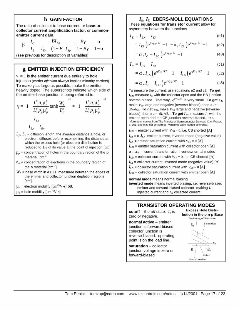
TRANSISTOR OPERATING MODES cutoff – the off state. IB is zero or negative.
normal active – emitter junction is forward-biased; collector junction is reverse-biased. operating point is on the load line.
saturation – collector junction voltage is zero or forward-biased
Excess Hole Distri-bution in the p-n-p Base
δp
0
Normal Active
nx
WCutoff
b
Saturation
Beginning of Saturation
Tom Penick [email protected] www.teicontrols.com/notes 1/14/2001 Page 18 of 23
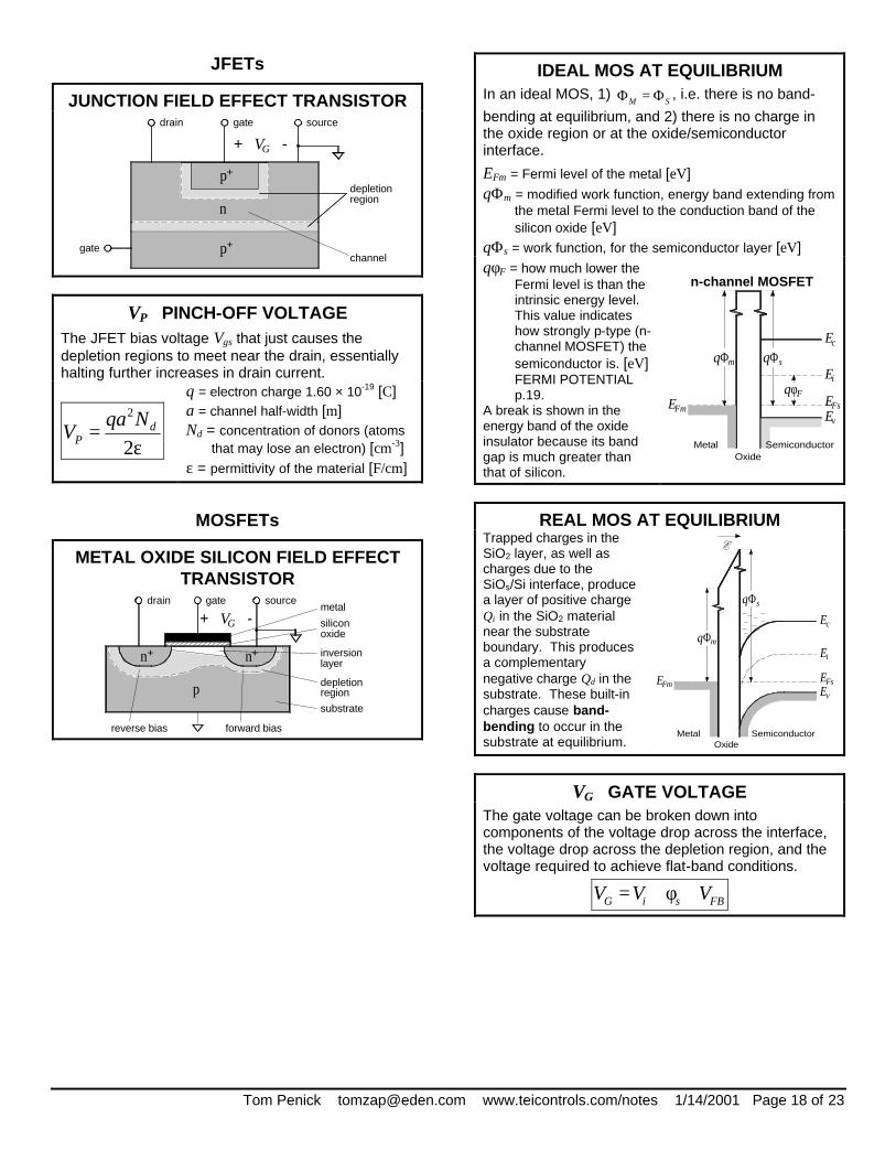
JFETs
JUNCTION FIELD EFFECT TRANSISTOR
V
gate
drain
n
+p
+
+p
gate source
G -
depletionregion
channel
VP PINCH-OFF VOLTAGE The JFET bias voltage Vgs that just causes the depletion regions to meet near the drain, essentially halting further increases in drain current.
ε=
2
2d
P
NqaV
q = electron charge 1.60 × 10⁻¹⁹ [C] a = channel half-width [m] Nd = concentration of donors (atoms
that may lose an electron) [cm-3] ε = permittivity of the material [F/cm]
MOSFETs
METAL OXIDE SILICON FIELD EFFECT TRANSISTOR
metaldrain sourcegate
+ VG - siliconoxide
forward biasreverse bias
+n
p
+n
substrate
depletionregion
inversionlayer
IDEAL MOS AT EQUILIBRIUM In an ideal MOS, 1)
M SΦ = Φ , i.e. there is no band-
bending at equilibrium, and 2) there is no charge in the oxide region or at the oxide/semiconductor interface.
EFm = Fermi level of the metal [eV] qΦm = modified work function, energy band extending from
the metal Fermi level to the conduction band of the silicon oxide [eV]
qΦs = work function, for the semiconductor layer [eV] qφF = how much lower the
Fermi level is than the intrinsic energy level. This value indicates how strongly p-type (n-channel MOSFET) the semiconductor is. [eV] FERMI POTENTIAL p.19.
A break is shown in the energy band of the oxide insulator because its band gap is much greater than that of silicon.
n-channel MOSFET
EFm
OxideMetal
qΦsqΦmEi
Ec
EEFs
v
qφF
Semiconductor
REAL MOS AT EQUILIBRIUM Trapped charges in the SiO2 layer, as well as charges due to the SiOs/Si interface, produce a layer of positive charge Qi in the SiO2 material near the substrate boundary. This produces a complementary negative charge Qd in the substrate. These built-in charges cause band-bending to occur in the substrate at equilibrium.
q mΦ
E
Ev
E
E
E
c
Fs
i
OxideMetal
qΦs
Semiconductor
FmE
VG GATE VOLTAGE The gate voltage can be broken down into components of the voltage drop across the interface, the voltage drop across the depletion region, and the voltage required to achieve flat-band conditions.
G i s FBV V V= + φ +

Tom Penick [email protected] www.teicontrols.com/notes 1/14/2001 Page 19 of 23
VT THRESHOLD VOLTAGE The minimum gate voltage of a MOSFET required to induce the channel. n-channel MOSFET: VT is positive or slightly negative because the first two terms (with their operators) are negative and the last two positive. When an n-channel MOSFET has a negative VT it means that the channel is made (the MOSFET conducts) until a negative gate voltage is applied. p-channel MOSFET: VT is negative because all terms (with their operators) are negative.
Fi
d
i
imsT C
QCQ
V φ+−−Φ= 2 i
aF n
N
qkT
ln=φ
Φms = metal semiconductor work function potential difference [V]
Qi = interface charge per unit area [C/cm2] p.20.
Qd = depletion region charge per unit area [C/cm2] p.20.
Ci = interface capacitance per unit area [F/cm2] p.20. φF = Fermi potential; Ei – EF, [V] p.19.
ADJUSTING VT BY ION IMPLANTATION The threshold voltage can be made less negative/more positive by implanting boron acceptors just below the Si surface near the gate in both n-channel and p-channel MOSFETs.
( ) ( .)B
T new T origi
qFV V
C= +
FB = boron doping concentration per unit area [cm-2] Ci = interface capacitance per unit area [F/cm2] p.20.
VFB FLAT BAND VOLTAGE The negative voltage required to straighten the energy bands. Trapped charges in the SiO2 layer, as well as charges due to the SiOs/Si interface, produce a layer of positive charge Qi in the SiO2 material near the substrate boundary (n-channel and p-channel MOSFETs). This produces a complementary negative charge Qd in the substrate. When the (negative) flat band voltage is applied to the gate, an electric field is set up between the positive charges in the SiO2 layer and the negative charges on the gate, eliminating the negative charges Qd in the substrate.
i
imsFB C
QV −Φ=
Φms = metal semiconductor work function voltage [V]
Qi = effective MOS interface charge per unit area; the naturally occurring charge in the SiO2 layer. Dr. Kwong prefers to call this Qox. [C/cm2]
Ci = interface capacitance per unit area [F/cm2] p.20.
Vi INTERFACE VOLTAGE The voltage drop across the SiO2 insulator. Dr. Kwong prefers to call this Vox.
s si
i i
Q d QV
C− −
= =ε
φs = surface potential [V] p.20. Qs = the negative charge density on the semiconductor
[C/cm2] d = thickness of the insulator [cm] VG = gate voltage [V] Ci = interface capacitance per unit area [F/cm2] p.20. εi = permittivity of the interface layer, 3.9ε0/100 for SiO2
[F/cm]
ΦΦms METAL SEMICONDUCTOR WORK FUNCTION [V]
The metal semiconductor work function is the voltage potential between the metal gate and the semiconductor body. Work function voltages vary with the material and the doping concentration. Also, see illustration at REAL MOS AT EQUILIBRIUM p.18.
ms m sΦ = Φ −Φ
Φm = work function voltage of the metal gate (high) [V]
Φs = work function voltage of the semiconductor (low) [V]
-0.2
0
-0.4
-0.6
-0.8
-1.0
10 1412 10 1016 1018
(cm )-3Nd a, N
Φms
(V)
Al to n-type Si
Al to p-type Si
φφF FERMI POTENTIAL [V] φF is the potential between the intrinsic energy level and the Fermi level. It is related to how strongly doped the semiconductor is. n-channel:
ln aF
i
NkTq n
φ =
/0
Fq kTip n e φ=
p-channel:
ln dF
i
NkTq n
φ = −
n-channel MOSFET
0 x = ∞
oxide
FE
vE
i
FE
φq
semiconductorcE
Tom Penick [email protected] www.teicontrols.com/notes 1/14/2001 Page 20 of 23
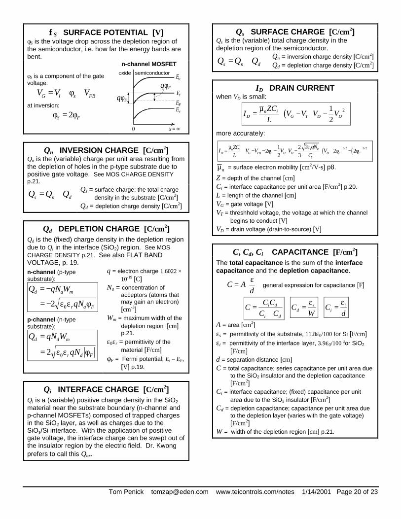
φφS SURFACE POTENTIAL [V] φS is the voltage drop across the depletion region of the semiconductor, i.e. how far the energy bands are bent.
φS is a component of the gate voltage:
G i s FBV V V= + φ +
at inversion:
2S Fφ = φ
n-channel MOSFET
0 x = ∞
φq S
oxide
v
i
F
c
F
E
EE
φq
semiconductorE
Qn INVERSION CHARGE [C/cm2] Qn is the (variable) charge per unit area resulting from the depletion of holes in the p-type substrate due to positive gate voltage. See MOS CHARGE DENSITY p.21.
s n dQ Q Q= +
Qs = surface charge; the total charge density in the substrate [C/cm2]
Qd = depletion charge density [C/cm2]
Qd DEPLETION CHARGE [C/cm2] Qd is the (fixed) charge density in the depletion region due to Qi in the interface (SiO2) region. See MOS CHARGE DENSITY p.21. See also FLAT BAND VOLTAGE, p. 19.
n-channel (p-type substrate):
Far
mad
qN
WqNQ
φεε−=
−=
02
p-channel (n-type substrate):
Fdr
mdd
qN
WqNQ
φεε=
=
02
q = electron charge 1.6022 × 10⁻¹⁹ [C]
Na = concentration of acceptors (atoms that may gain an electron) [cm-3]
Wm = maximum width of the depletion region [cm] p.21.
ε0εr = permittivity of the material [F/cm]
φF = Fermi potential; Ei – EF, [V] p.19.
Qi INTERFACE CHARGE [C/cm2] Qi is a (variable) positive charge density in the SiO2 material near the substrate boundary (n-channel and p-channel MOSFETs) composed of trapped charges in the SiO2 layer, as well as charges due to the SiOs/Si interface. With the application of positive gate voltage, the interface charge can be swept out of the insulator region by the electric field. Dr. Kwong prefers to call this Qox.
Qs SURFACE CHARGE [C/cm2] Qs is the (variable) total charge density in the depletion region of the semiconductor.
s n dQ Q Q= + Qn = inversion charge density [C/cm2] Qd = depletion charge density [C/cm2]
ID DRAIN CURRENT when VD is small:
( ) 21
2n i
D G T D D
ZCI V V V V
Lµ = − −
more accurately:
( ) ( )3/2 3/221 22 2 2
2 3s an i
D G FB F D D D F Fi
qNZCI V V V V V
L C
εµ = − − φ − − + φ − φ
nµ = surface electron mobility [cm2/V-s] p8.
Z = depth of the channel [cm] Ci = interface capacitance per unit area [F/cm2] p.20. L = length of the channel [cm] VG = gate voltage [V] VT = threshhold voltage, the voltage at which the channel
begins to conduct [V] VD = drain voltage (drain-to-source) [V]
C, Cd, Ci CAPACITANCE [F/cm2] The total capacitance is the sum of the interface capacitance and the depletion capacitance.
C Adε
= ⋅ general expression for capacitance [F]
i d
i d
C CC
C C=
+ s
dCWε
= iiC
dε
=
A = area [cm2] εs = permittivity of the substrate, 11.8ε0/100 for Si [F/cm] εi = permittivity of the interface layer, 3.9ε0/100 for SiO2
[F/cm] d = separation distance [cm] C = total capacitance; series capacitance per unit area due
to the SiO2 insulator and the depletion capacitance
[F/cm2] Ci = interface capacitance; (fixed) capacitance per unit
area due to the SiO2 insulator [F/cm2] Cd = depletion capacitance; capacitance per unit area due
to the depletion layer (varies with the gate voltage) [F/cm2]
W = width of the depletion region [cm] p.21.
Tom Penick [email protected] www.teicontrols.com/notes 1/14/2001 Page 21 of 23
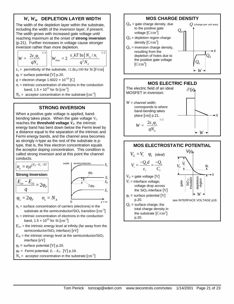
W, Wm DEPLETION LAYER WIDTH The width of the depletion layer within the substrate, including the width of the inversion layer, if present. The width grows with increased gate voltage until reaching maximum at the onset of strong inversion (p.21). Further increases in voltage cause stronger inversion rather than more depletion.
1/22 s s
a
WqN
ε φ=
( ) 1/ 2
max 2
ln /2 s a i
a
kT N nW
q N
ε =
εs = permittivity of the substrate, 11.8ε0/100 for Si [F/cm] φs = surface potential [V] p.20. q = electron charge 1.6022 × 10⁻¹⁹ [C] ni = intrinsic concentration of electrons in the conduction
band, 1.5 × 10¹⁰ for Si [cm-3] Na = acceptor concentration in the substrate [cm-3]
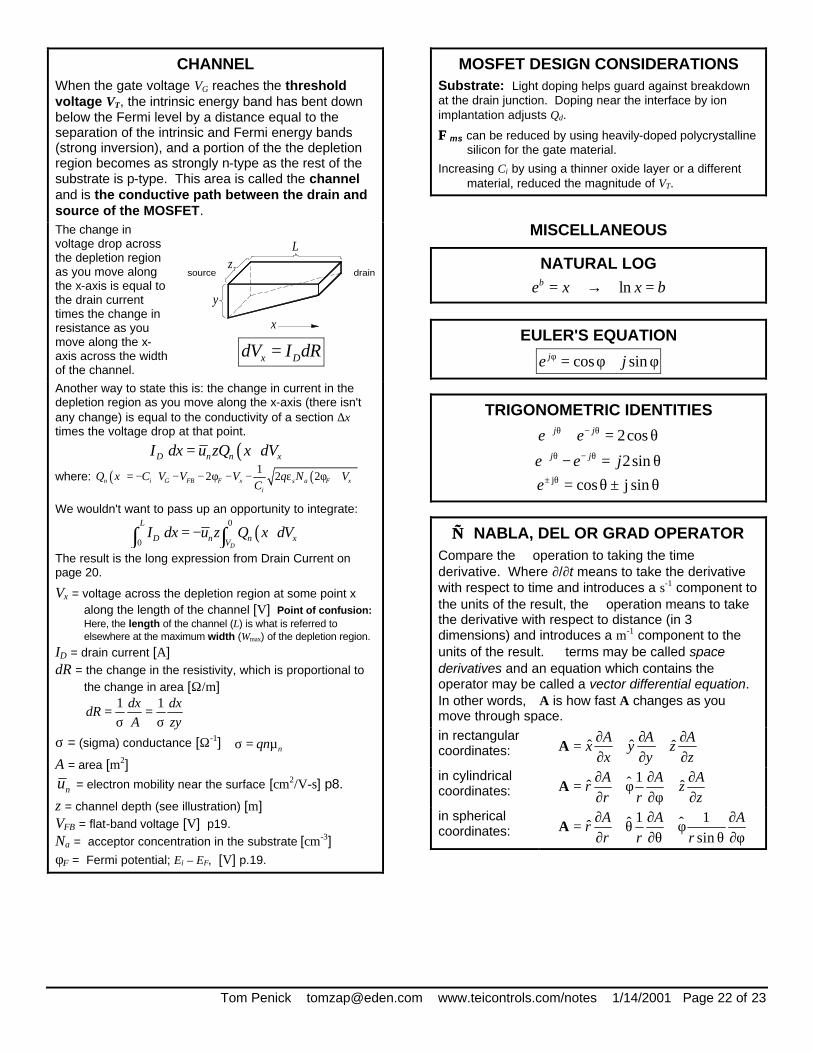
STRONG INVERSION When a positive gate voltage is applied, band-bending takes place. When the gate voltage VG reaches the threshold voltage VT, the intrinsic energy band has bent down below the Fermi level by a distance equal to the separation of the intrinsic and Fermi energy bands, and the channel area becomes as strongly n-type as the rest of the substrate is p-type, that is, the free electron concentration equals the acceptor doping concentration. This condition is called strong inversion and at this point the channel conducts.
( ) /F iE E kTs in n e −=
Strong Inversion:
0 2i iF
E Eq
∞ −= φ
2s F s An Nφ = φ ⇔ =
E
0
φq2 F
x= ∞
v
F
i
E
E
semiconductor oxide
Fqφ
cE
ns = surface concentration of carriers (electrons) in the
substrate at the semiconductor/SiO2 transition [cm-3] ni = intrinsic concentration of electrons in the conduction
band, 1.5 × 10¹⁰ for Si [cm-3] Ei∞ = the intrinsic energy level at infinity (far away from the
semiconductor/SiO2 interface) [eV] Ei0 = the intrinsic energy level at the semiconductor/SiO2
interface [eV] φs = surface potential [V] p.20. φF = Fermi potential; Ei – EF, [V] p.19. Na = acceptor concentration in the substrate [cm-3]
MOS CHARGE DENSITY Qm = gate charge density, due
to the positive gate voltage [C/cm2]
Qd = depletion region charge density [C/cm2]
Qn = inversion charge density, resulting from the depletion of holes due to the positive gate voltage [C/cm2]
Qd
W
Qn
Qm
x
(charge per unit area)Q
MOS ELECTRIC FIELD The electric field of an ideal MOSFET in inversion: W = channel width;
corresponds to where band-bending takes place [cm] p.21.
1/22 s s
a
WqN
ε φ=
W
x( )E
x
MOS ELECTROSTATIC POTENTIAL
G i sV V= + φ (ideal)
s si
i i
Q d QV
C− −
= =ε
VG = gate voltage [V] Vi = interface voltage;
voltage drop across the SiO2 interface [V]
φs = surface potential [V] p.20.
Qs = surface charge; the total charge density in the substrate [C/cm2] p.20.
deple
tion
regio
n
Vi
gate
SiO
in
sula
tor
VG
2
x( )V
φ
W
x
s
see INTERFACE VOLTAGE p19.
Tom Penick [email protected] www.teicontrols.com/notes 1/14/2001 Page 22 of 23
CHANNEL When the gate voltage VG reaches the threshold voltage VT, the intrinsic energy band has bent down below the Fermi level by a distance equal to the separation of the intrinsic and Fermi energy bands (strong inversion), and a portion of the the depletion region becomes as strongly n-type as the rest of the substrate is p-type. This area is called the channel and is the conductive path between the drain and source of the MOSFET. The change in voltage drop across the depletion region as you move along the x-axis is equal to the drain current times the change in resistance as you move along the x-axis across the width of the channel.
z
x
y
source
L
drain
x DdV I dR=
Another way to state this is: the change in current in the depletion region as you move along the x-axis (there isn't any change) is equal to the conductivity of a section ∆x times the voltage drop at that point.
( )D n n xI dx u zQ x dV=
where: ( ) ( )12 2 2n i G FB F x s a F x
i
Q x C V V V q N VC
= − − − φ − − ε φ +
We wouldn't want to pass up an opportunity to integrate:
( )0
0 D
L
D n n xVI dx u z Q x dV= −∫ ∫
The result is the long expression from Drain Current on page 20.
Vx = voltage across the depletion region at some point x along the length of the channel [V] Point of confusion: Here, the length of the channel (L) is what is referred to elsewhere at the maximum width (Wmax) of the depletion region.
ID = drain current [A] dR = the change in the resistivity, which is proportional to
the change in area [Ω/m]
1 1dx dxdR
A zy= =
σ σ
σ = (sigma) conductance [Ω-1] nqnσ = µ
A = area [m2]
nu = electron mobility near the surface [cm2/V-s] p8.
z = channel depth (see illustration) [m] VFB = flat-band voltage [V] p19.
Na = acceptor concentration in the substrate [cm-3] φF = Fermi potential; Ei – EF, [V] p.19.
MOSFET DESIGN CONSIDERATIONS Substrate: Light doping helps guard against breakdown at the drain junction. Doping near the interface by ion implantation adjusts Qd.
ΦΦms can be reduced by using heavily-doped polycrystalline silicon for the gate material.
Increasing Ci by using a thinner oxide layer or a different material, reduced the magnitude of VT.
MISCELLANEOUS
NATURAL LOG
lnbe x x b= → =
EULER'S EQUATION
cos sinje jφ = φ + φ
TRIGONOMETRIC IDENTITIES
2cosj je e+ θ − θ+ = θ
2sinj je e j+ θ − θ− = θ j cos j sine± θ = θ ± θ
∇ ∇ NABLA, DEL OR GRAD OPERATOR Compare the ∇ operation to taking the time derivative. Where ∂/∂t means to take the derivative with respect to time and introduces a s-1 component to the units of the result, the ∇ operation means to take the derivative with respect to distance (in 3 dimensions) and introduces a m-1 component to the units of the result. ∇ terms may be called space derivatives and an equation which contains the ∇ operator may be called a vector differential equation. In other words, ∇A is how fast A changes as you move through space.
in rectangular coordinates: ˆ ˆ ˆ
A A Ax y z
x y z∂ ∂ ∂
∇ = + +∂ ∂ ∂
A
in cylindrical coordinates:
1ˆˆ ˆA A A
r zr r z
∂ ∂ ∂∇ = + φ +
∂ ∂φ ∂A
in spherical coordinates:
1 1ˆ ˆˆsin
A A Ar
r r r∂ ∂ ∂
∇ = + θ + φ∂ ∂θ θ ∂φ
A
Tom Penick [email protected] www.teicontrols.com/notes 1/14/2001 Page 23 of 23
∇∇2 THE LAPLACIAN The divergence of a gradient
Laplacian of a scalar in rectangular coordinates:
2 2 22
2 2 2
A A AA
x y z∂ ∂ ∂
∇ = + +∂ ∂ ∂
Laplacian of a vector in rectan-gular coordinates:
22 22
2 2 2ˆ ˆ ˆyx z
AA AA x y z
x y z
∂∂ ∂∇ = + +
∂ ∂ ∂
v
In spherical and cylindrical coordinates:
( )( ) ( )AA
AAA
curlcurldivgrad
·2
−=×∇×∇−∇∇≡∇
DOT PRODUCT The dot product is a scalar value.
( ) ( )•
ˆ ˆ ˆ ˆ ˆ ˆ•x y z x y z x x y y z zA A A B B B A B A B A B
=
+ + + + = + +
A B
x y z x y z
ABcos• ψ= BABA
0ˆ•ˆ =yx , 1ˆ•ˆ =xx
( ) yzyx BBBB =++= yzyxyB ˆ•ˆˆˆˆ•
ψ
B
A
A•B Projection of B along â:
( )aaB ˆˆ•
B
ψâ
â
ψ
B
The dot product is commutative and distributive:
ABBA •• = ( ) CABACBA ••• +=+
CROSS PRODUCT ( ) ( )
( ) ( ) ( )xyyxzxxzyzzy
zyxzyx
BABABABABABA
BBBAAA
−+−+−=
++×++=×
zyx
zyxzyxBA
ˆˆˆ
ˆˆˆˆˆˆ
ABsinˆ ψ=× BAnBA
where n is the unit vector normal to both A and B (thumb of right-hand rule).
BAAB ×−=×
The cross product is distributive: ( ) CABACBA ×+×=+×
n
ψ
A×B
A
B
CONSTANTS
Avogadro’s number
[molecules/mole] 231002.6 ×=AN
Boltzmann’s constant 231038.1 −×=k J/K
or 51062.8 −×=K eV/K
Elementary charge 191.6022 10q −= × C
Electron mass 310 1011.9 −×=m kg
Permittivity of free space 140 1085.8 −×=ε F/cm
120 8.85 10−ε = × F/m
Planck’s constant 341063.6 −×=h J-s
151014.4 −×= eV-s
also, /(2 )h= πh
Rydberg constant 678,109=R cm-1
kT @ room temperature 0259.0=kT eV
Speed of light 1010998.2 ×=c cm/s
1 Å (angstrom) 10-8 cm = 10-10 M
1 µm (micron) 10-4 cm 1 nm = 10Å = 10-7 cm 1 eV = 1.6022 × 10⁻¹⁹ J 1 W = 1 J/S = 1 VA 1 V = 1 J/C 1 N/C = 1 V/m 1 J = 1 N· m = 1
C· V
EXPANSIONS FOR HYPERBOLIC FUNCTIONS
2 45sech 1
2 24y y
y = − + −L
31ctnh
3 45y y
yy
= + − +L
31 7csch
6 360y y
yy
= − + −L
3
tanh 3y
y y= − +L