Embed Size (px)
Citation preview
DATA SHEET
Clock Generator for Cavium Processors IDT8V41N012I
IDT8V41N012NLGI REVISION A JULY 18, 2013 1 ©2013 Integrated Device Technology, Inc.
General Description
The IDT8V41N012I is a PLL-based clock generator specifically de-signed for Cavium Networks Octeon II processors. This high perfor-mance device is optimized to generate the processor core referenceclock, the PCI-Express, sRIO, XAUI, SerDes reference clocks andthe clocks for both the Gigabit Ethernet MAC and PHY. The outputfrequencies are generated from a 25MHz external input source or anexternal 25MHz parallel resonant crystal. The industrial temperaturerange of the IDT8V41N012I supports telecommunication, network-ing, and storage requirements.
Features
• Ten selectable 100MHz, 125MHz, 156.25MHz and 312.5MHzclocks for PCI Express, sRIO and GbE, HCSL interface levels
• One single-ended QG LVCMOS/LVTTL clock output at 125MHz
• One single-ended QF LVCMOS/LVTTL clock output at 50MHz
• Two single-ended QREFx LVCMOS/LVTTL outputs at 25MHz
• Selectable external crystal or differential (single-ended)input source
• Crystal oscillator interface designed for 25MHz, parallelresonant crystal
• Differential CLK, nCLK input pair that can accept: LVPECL, LVDS,LVHSTL, HCSL input levels
• Internal resistor bias on nCLK pin allows the user to drive CLKinput with external single-ended (LVCMOS/ LVTTL) input levels
• Supply Modes, (125MHz QG output and 25MHz QREFx outputs):Core / Output3.3V / 3.3V3.3V / 2.5V
• Supply Modes, (HCSL outputs, and 50MHz QF output):Core / Output3.3V / 3.3V
• -40°C to 85°C ambient operating temperature
• Lead-free (RoHS 6) packaging
Pin Assignment
NOTE: Exposed pad must always be connected to GND.NOTE: Pin 1 is located at bottom left corner as shown.
46 47 48 49 50 51 52 53 54 45 44 43 42 41 40 39 38 37
1 2 3 4 5 6 7 8 9 10 11 12 13 14 15 16 17 18
5556
5758
596061
626364
656667
68
697071
72
303132
333435
36
292827
262524
2322
212019
QE0
OE_G
nQE0QE1
GND
OE_EFSEL_C0FSEL_C1
nQE1
QG
VDDA
GND
FSEL_D0
FSEL_D1VDD
nMR
VDDO_QG
GND
QB1nQB0
QB0
nQB1
VDDO_QB
GND
OE_AGND
GND
nQA1QA1
nQA0
VDDO_QF
QF
QA0VDDO_QA
GND
VDD
OE
_RE
F
FS
EL_
B1
CLK
FS
EL_
A0
VD
DO
_QR
EF
QR
EF
0
QR
EF
1
GN
DF
SE
L_E
0
FS
EL_
E1
FS
EL_
B0
RE
F_S
EL
VD
D
nC
LK
XTA
L_IN
XTA
L_O
UT
PLL
_SE
L
FS
EL_
A1
IRE
FO
E_D
GN
D
nQD
1Q
D1
nQD
0Q
D0
VD
DO
_QC
VD
DO
_QD
QC
0
VD
D
OE
_CG
ND
nQC
1
nQC
0Q
C1
VD
DO
_QE
OE
_B
IDT8V41N012I
72-Lead VFQFN10mm x 10mm x 0.90mm
package body6mm x 6mm EPad
NL package
Top View
IDT8V41N012I DATA SHEET CLOCK GENERATOR FOR CAVIUM PROCESSORS
IDT8V41N012NLGI REVISION A JULY 18, 2013 2 ©2013 Integrated Device Technology, Inc.
Block Diagram
IDT8V41N012I DATA SHEET CLOCK GENERATOR FOR CAVIUM PROCESSORS
IDT8V41N012NLGI REVISION A JULY 18, 2013 3 ©2013 Integrated Device Technology, Inc.
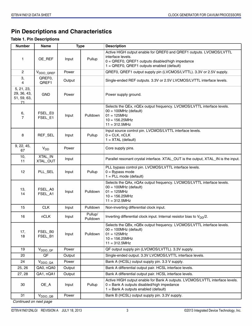
Pin Descriptions and CharacteristicsTable 1. Pin Descriptions
Number Name Type Description
1 OE_REF Input Pullup
Active HIGH output enable for QREF0 and QREF1 outputs. LVCMOS/LVTTLinterface levels.0 = QREF0, QREF1 outputs disabled/high impedance1 = QREF0, QREF1 outputs enabled (default)
2 VDDO_QREF Power QREF0, QREF1 output supply pin (LVCMOS/LVTTL). 3.3V or 2.5V supply.
3,4
QREF0,QREF1
Output Single-ended REF outputs. 3.3V or 2.5V LVCMOS/LVTTL interface levels.
5, 21, 23,29, 36, 43,51, 59, 63,
71
GND Power Power supply ground.
6,7
FSEL_E0FSEL_E1
Input Pulldown
Selects the QEx, nQEx output frequency. LVCMOS/LVTTL interface levels.00 = 100MHz (default)01 = 125MHz10 = 156.25MHz11 = 312.5MHz
8 REF_SEL Input PullupInput source control pin. LVCMOS/LVTTL interface levels.0 = CLK, nCLK1 = XTAL (default)
9, 22, 45,67
VDD Power Core supply pins.
10,11
XTAL_INXTAL_OUT
Input Parallel resonant crystal interface. XTAL_OUT is the output, XTAL_IN is the input.
12 PLL_SEL Input PullupPLL bypass control pin. LVCMOS/LVTTL interface levels.0 = Bypass mode1 = PLL mode (default)
13,14
FSEL_A0FSEL_A1
Input Pulldown
Selects the QAx, nQAx output frequency. LVCMOS/LVTTL interface levels.00 = 100MHz (default)01 = 125MHz10 = 156.25MHz11 = 312.5MHz
15 CLK Input Pulldown Non-inverting differential clock input.
16 nCLK InputPullup/
PulldownInverting differential clock input. Internal resistor bias to VDD/2.
17,18
FSEL_B0FSEL_B1
Input Pulldown
Selects the QBx, nQBx output frequency. LVCMOS/LVTTL interface levels.00 = 100MHz (default)01 = 125MHz10 = 156.25MHz11 = 312.5MHz
19 VDDO_QF Power QF output supply pin (LVCMOS/LVTTL). 3.3V supply.
20 QF Output Single-ended output. 3.3V LVCMOS/LVTTL interface levels.
24 VDDO_QA Power Bank A (HCSL) output supply pin. 3.3 V supply.
25, 26 QA0, nQA0 Output Bank A differential output pair. HCSL interface levels.
27, 28 QA1, nQA1 Output Bank A differential output pair. HCSL interface levels.
30 OE_A Input PullupActive HIGH output enable for Bank A outputs. LVCMOS/LVTTL interface levels.0 = Bank A outputs disabled/high impedance1 = Bank A outputs enabled (default)
31 VDDO_QB Power Bank B (HCSL) output supply pin. 3.3V supply.
Continued on next page
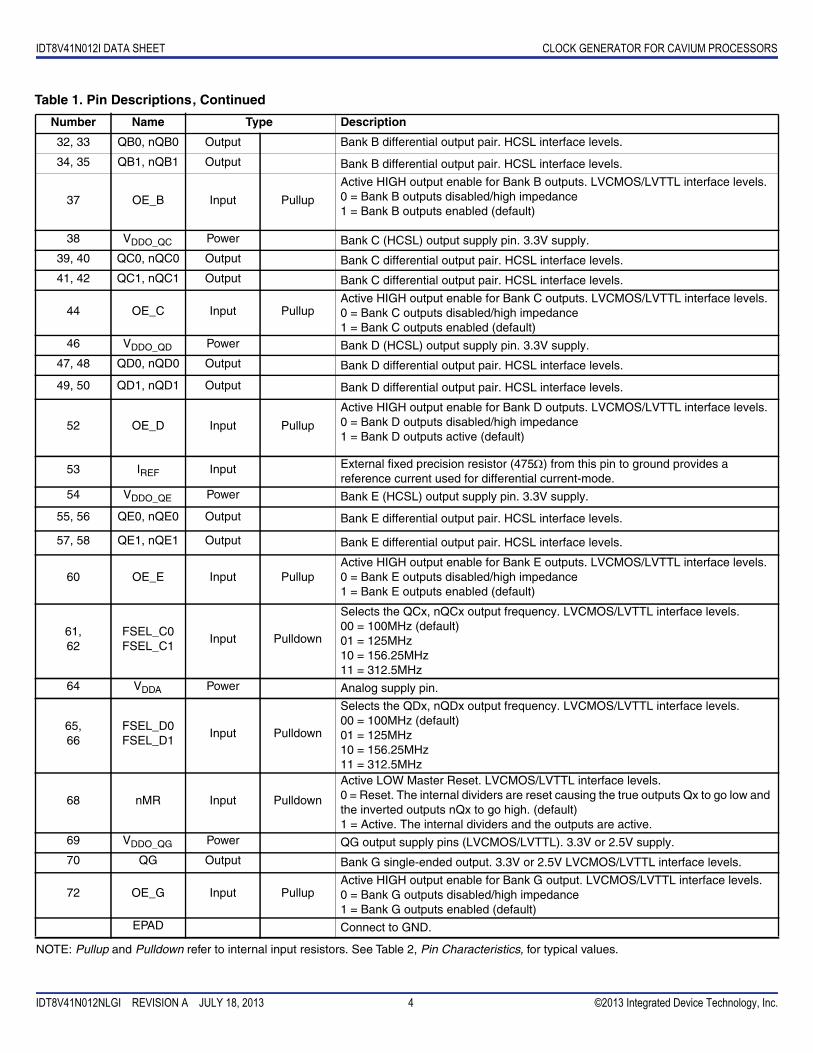
IDT8V41N012I DATA SHEET CLOCK GENERATOR FOR CAVIUM PROCESSORS
IDT8V41N012NLGI REVISION A JULY 18, 2013 4 ©2013 Integrated Device Technology, Inc.
NOTE: Pullup and Pulldown refer to internal input resistors. See Table 2, Pin Characteristics, for typical values.
32, 33 QB0, nQB0 Output Bank B differential output pair. HCSL interface levels.
34, 35 QB1, nQB1 Output Bank B differential output pair. HCSL interface levels.
37 OE_B Input Pullup
Active HIGH output enable for Bank B outputs. LVCMOS/LVTTL interface levels.0 = Bank B outputs disabled/high impedance1 = Bank B outputs enabled (default)
38 VDDO_QC Power Bank C (HCSL) output supply pin. 3.3V supply.
39, 40 QC0, nQC0 Output Bank C differential output pair. HCSL interface levels.
41, 42 QC1, nQC1 Output Bank C differential output pair. HCSL interface levels.
44 OE_C Input PullupActive HIGH output enable for Bank C outputs. LVCMOS/LVTTL interface levels.0 = Bank C outputs disabled/high impedance1 = Bank C outputs enabled (default)
46 VDDO_QD Power Bank D (HCSL) output supply pin. 3.3V supply.
47, 48 QD0, nQD0 Output Bank D differential output pair. HCSL interface levels.
49, 50 QD1, nQD1 Output Bank D differential output pair. HCSL interface levels.
52 OE_D Input Pullup
Active HIGH output enable for Bank D outputs. LVCMOS/LVTTL interface levels.0 = Bank D outputs disabled/high impedance1 = Bank D outputs active (default)
53 IREF Input External fixed precision resistor (475) from this pin to ground provides areference current used for differential current-mode.
54 VDDO_QE Power Bank E (HCSL) output supply pin. 3.3V supply.
55, 56 QE0, nQE0 Output Bank E differential output pair. HCSL interface levels.
57, 58 QE1, nQE1 Output Bank E differential output pair. HCSL interface levels.
60 OE_E Input PullupActive HIGH output enable for Bank E outputs. LVCMOS/LVTTL interface levels.0 = Bank E outputs disabled/high impedance1 = Bank E outputs enabled (default)
61,62
FSEL_C0FSEL_C1
Input Pulldown
Selects the QCx, nQCx output frequency. LVCMOS/LVTTL interface levels.00 = 100MHz (default)01 = 125MHz10 = 156.25MHz11 = 312.5MHz
64 VDDA Power Analog supply pin.
65,66
FSEL_D0FSEL_D1
Input Pulldown
Selects the QDx, nQDx output frequency. LVCMOS/LVTTL interface levels.00 = 100MHz (default)01 = 125MHz10 = 156.25MHz11 = 312.5MHz
68 nMR Input Pulldown
Active LOW Master Reset. LVCMOS/LVTTL interface levels.0 = Reset. The internal dividers are reset causing the true outputs Qx to go low andthe inverted outputs nQx to go high. (default)1 = Active. The internal dividers and the outputs are active.
69 VDDO_QG Power QG output supply pins (LVCMOS/LVTTL). 3.3V or 2.5V supply.
70 QG Output Bank G single-ended output. 3.3V or 2.5V LVCMOS/LVTTL interface levels.
72 OE_G Input PullupActive HIGH output enable for Bank G output. LVCMOS/LVTTL interface levels.0 = Bank G outputs disabled/high impedance1 = Bank G outputs enabled (default)
EPAD Connect to GND.
Table 1. Pin Descriptions
Number Name Type Description
, Continued
IDT8V41N012I DATA SHEET CLOCK GENERATOR FOR CAVIUM PROCESSORS
IDT8V41N012NLGI REVISION A JULY 18, 2013 5 ©2013 Integrated Device Technology, Inc.
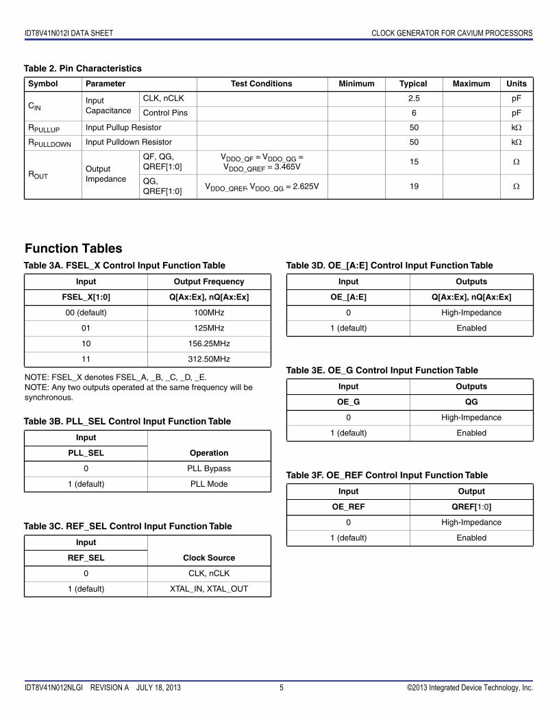
Table 2. Pin Characteristics
Function TablesTable 3A. FSEL_X Control Input Function Table
NOTE: FSEL_X denotes FSEL_A, _B, _C, _D, _E.NOTE: Any two outputs operated at the same frequency will besynchronous.
Table 3B. PLL_SEL Control Input Function Table
Table 3C. REF_SEL Control Input Function Table
Table 3D. OE_[A:E] Control Input Function Table
Table 3E. OE_G Control Input Function Table
Table 3F. OE_REF Control Input Function Table
Symbol Parameter Test Conditions Minimum Typical Maximum Units
CINInputCapacitance
CLK, nCLK 2.5 pF
Control Pins 6 pF
RPULLUP Input Pullup Resistor 50 k
RPULLDOWN Input Pulldown Resistor 50 k
ROUTOutputImpedance
QF, QG,QREF[1:0]
VDDO_QF = VDDO_QG =VDDO_QREF = 3.465V
15
QG,QREF[1:0]
VDDO_QREF, VDDO_QG = 2.625V 19
Input Output Frequency
FSEL_X[1:0] Q[Ax:Ex], nQ[Ax:Ex]
00 (default) 100MHz
01 125MHz
10 156.25MHz
11 312.50MHz
Input
OperationPLL_SEL
0 PLL Bypass
1 (default) PLL Mode
Input
Clock SourceREF_SEL
0 CLK, nCLK
1 (default) XTAL_IN, XTAL_OUT
Input Outputs
OE_[A:E] Q[Ax:Ex], nQ[Ax:Ex]
0 High-Impedance
1 (default) Enabled
Input Outputs
OE_G QG
0 High-Impedance
1 (default) Enabled
Input Output
OE_REF QREF[1:0]
0 High-Impedance
1 (default) Enabled
IDT8V41N012I DATA SHEET CLOCK GENERATOR FOR CAVIUM PROCESSORS
IDT8V41N012NLGI REVISION A JULY 18, 2013 6 ©2013 Integrated Device Technology, Inc.
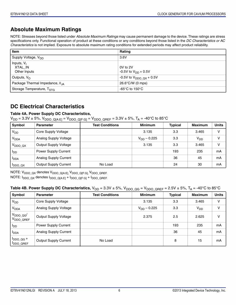
Absolute Maximum RatingsNOTE: Stresses beyond those listed under Absolute Maximum Ratings may cause permanent damage to the device. These ratings are stressspecifications only. Functional operation of product at these conditions or any conditions beyond those listed in the DC Characteristics or ACCharacteristics is not implied. Exposure to absolute maximum rating conditions for extended periods may affect product reliability.
DC Electrical CharacteristicsTable 4A. Power Supply DC Characteristics,VDD = 3.3V ± 5%, VDDO_Q[A:E] = VDDO_Q[F:G] = VDDO_QREF = 3.3V ± 5%, TA = -40°C to 85°C
NOTE: VDDO_QX denotes VDDO_Q[A:E], VDDO_Q[F:G], VDDO_QREF.
NOTE: IDDO_QX denotes IDDO_Q[A:E] + IDDO_Q[F:G] + IDDO_QREF.
Table 4B. Power Supply DC Characteristics, VDD = 3.3V ± 5%, VDDO_QG = VDDO_QREF = 2.5V ± 5%, TA = -40°C to 85°C
Item Rating
Supply Voltage, VDD 3.6V
Inputs, VIXTAL_INOther Inputs
0V to 2V-0.5V to VDD + 0.5V
Outputs, VO -0.5V to VDDO_QX + 0.5V
Package Thermal Impedance, JA 26.6°C/W (0 mps)
Storage Temperature, TSTG -65C to 150C
Symbol Parameter Test Conditions Minimum Typical Maximum Units
VDD Core Supply Voltage 3.135 3.3 3.465 V
VDDA Analog Supply Voltage VDD – 0.225 3.3 VDD V
VDDO_QX Output Supply Voltage 3.135 3.3 3.465 V
IDD Power Supply Current 193 235 mA
IDDA Analog Supply Current 36 45 mA
IDDO_QX Output Supply Current No Load 24 30 mA
Symbol Parameter Test Conditions Minimum Typical Maximum Units
VDD Core Supply Voltage 3.135 3.3 3.465 V
VDDA Analog Supply Voltage VDD – 0.225 3.3 VDD V
VDDO_QG/VDDO_QREF
Output Supply Voltage 2.375 2.5 2.625 V
IDD Power Supply Current 193 235 mA
IDDA Analog Supply Current 36 45 mA
IDDO_QG +IDDO_QREF
Output Supply Current No Load 8 15 mA
IDT8V41N012I DATA SHEET CLOCK GENERATOR FOR CAVIUM PROCESSORS
IDT8V41N012NLGI REVISION A JULY 18, 2013 7 ©2013 Integrated Device Technology, Inc.
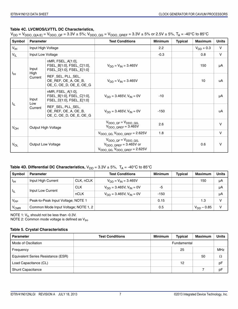
Table 4C. LVCMOS/LVTTL DC Characteristics,VDD = VDDO_Q[A:E] = VDDO_QF = 3.3V ± 5%; VDDO_QG = VDDO_QREF = 3.3V ± 5% or 2.5V ± 5%, TA = -40°C to 85°C
Table 4D. Differential DC Characteristics, VDD = 3.3V ± 5%, TA = -40°C to 85°C
NOTE 1: VIL should not be less than -0.3V.NOTE 2: Common mode voltage is defined as VIH.
Table 5. Crystal Characteristics
Symbol Parameter Test Conditions Minimum Typical Maximum Units
VIH Input High Voltage 2.2 VDD + 0.3 V
VIL Input Low Voltage -0.3 0.8 V
IIH
InputHighCurrent
nMR, FSEL_A[1:0],FSEL_B[1:0], FSEL_C[1:0],FSEL_D[1:0], FSEL_E[1:0]
VDD = VIN = 3.465V 150 µA
REF_SEL, PLL_SEL,OE_REF, OE_A, OE_B,OE_C, OE_D, OE_E, OE_G
VDD = VIN = 3.465V 10 uA
IIL
InputLowCurrent
nMR, FSEL_A[1:0],FSEL_B[1:0], FSEL_C[1:0],FSEL_D[1:0], FSEL_E[1:0]
VDD = 3.465V, VIN = 0V -10 µA
REF_SEL, PLL_SEL,OE_REF, OE_A, OE_B,OE_C, OE_D, OE_E, OE_G
VDD = 3.465V, VIN = 0V -150 uA
VOH Output High Voltage
VDDO_QF = VDDO_QG,VDDO_QREF = 3.465V
2.6 V
VDDO_QG, VDDO_QREF = 2.625V 1.8 V
VOL Output Low VoltageVDDO_QF = VDDO_QG,
VDDO_QREF = 3.465V orVDDO_QG, VDDO_QREF = 2.625V
0.6 V
Symbol Parameter Test Conditions Minimum Typical Maximum Units
IIH Input High Current CLK, nCLK VDD = VIN = 3.465V 150 µA
IIL Input Low CurrentCLK VDD = 3.465V, VIN = 0V -5 µA
nCLK VDD = 3.465V, VIN = 0V -150 µA
VPP Peak-to-Peak Input Voltage; NOTE 1 0.15 1.3 V
VCMR Common Mode Input Voltage; NOTE 1, 2 0.5 VDD – 0.85 V
Parameter Test Conditions Minimum Typical Maximum Units
Mode of Oscillation Fundamental
Frequency 25 MHz
Equivalent Series Resistance (ESR) 50
Load Capacitance (CL) 12 pF
Shunt Capacitance 7 pF
IDT8V41N012I DATA SHEET CLOCK GENERATOR FOR CAVIUM PROCESSORS
IDT8V41N012NLGI REVISION A JULY 18, 2013 8 ©2013 Integrated Device Technology, Inc.
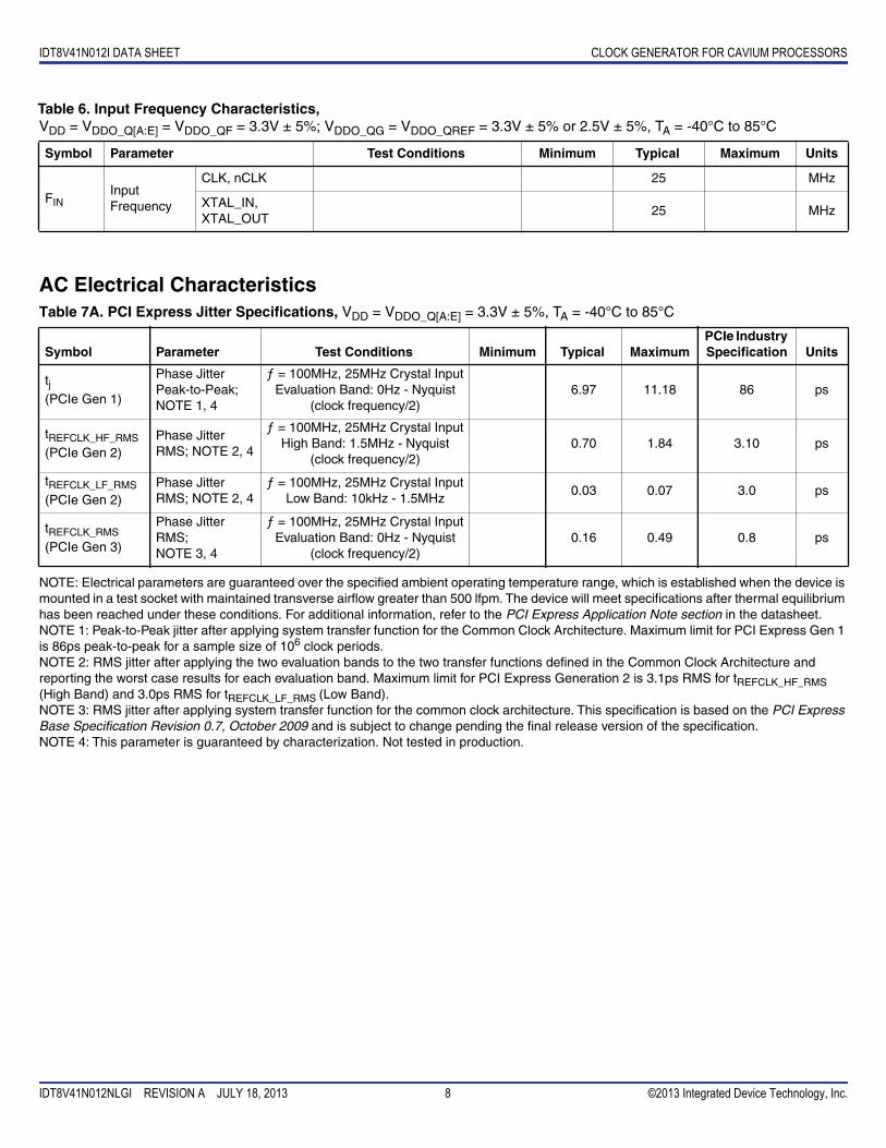
Table 6. Input Frequency Characteristics,VDD = VDDO_Q[A:E] = VDDO_QF = 3.3V ± 5%; VDDO_QG = VDDO_QREF = 3.3V ± 5% or 2.5V ± 5%, TA = -40°C to 85°C
AC Electrical CharacteristicsTable 7A. PCI Express Jitter Specifications, VDD = VDDO_Q[A:E] = 3.3V ± 5%, TA = -40°C to 85°C
NOTE: Electrical parameters are guaranteed over the specified ambient operating temperature range, which is established when the device ismounted in a test socket with maintained transverse airflow greater than 500 lfpm. The device will meet specifications after thermal equilibriumhas been reached under these conditions. For additional information, refer to the PCI Express Application Note section in the datasheet.NOTE 1: Peak-to-Peak jitter after applying system transfer function for the Common Clock Architecture. Maximum limit for PCI Express Gen 1is 86ps peak-to-peak for a sample size of 106 clock periods.NOTE 2: RMS jitter after applying the two evaluation bands to the two transfer functions defined in the Common Clock Architecture andreporting the worst case results for each evaluation band. Maximum limit for PCI Express Generation 2 is 3.1ps RMS for tREFCLK_HF_RMS(High Band) and 3.0ps RMS for tREFCLK_LF_RMS (Low Band).NOTE 3: RMS jitter after applying system transfer function for the common clock architecture. This specification is based on the PCI ExpressBase Specification Revision 0.7, October 2009 and is subject to change pending the final release version of the specification.NOTE 4: This parameter is guaranteed by characterization. Not tested in production.
Symbol Parameter Test Conditions Minimum Typical Maximum Units
FINInputFrequency
CLK, nCLK 25 MHz
XTAL_IN,XTAL_OUT
25 MHz
Symbol Parameter Test Conditions Minimum Typical MaximumPCIe IndustrySpecification Units
tj(PCIe Gen 1)
Phase JitterPeak-to-Peak;NOTE 1, 4
ƒ = 100MHz, 25MHz Crystal InputEvaluation Band: 0Hz - Nyquist
(clock frequency/2)6.97 11.18 86 ps
tREFCLK_HF_RMS
(PCIe Gen 2)Phase JitterRMS; NOTE 2, 4
ƒ = 100MHz, 25MHz Crystal InputHigh Band: 1.5MHz - Nyquist
(clock frequency/2)0.70 1.84 3.10 ps
tREFCLK_LF_RMS
(PCIe Gen 2)Phase JitterRMS; NOTE 2, 4
ƒ = 100MHz, 25MHz Crystal InputLow Band: 10kHz - 1.5MHz
0.03 0.07 3.0 ps
tREFCLK_RMS
(PCIe Gen 3)
Phase JitterRMS;NOTE 3, 4
ƒ = 100MHz, 25MHz Crystal InputEvaluation Band: 0Hz - Nyquist
(clock frequency/2)0.16 0.49 0.8 ps
IDT8V41N012I DATA SHEET CLOCK GENERATOR FOR CAVIUM PROCESSORS
IDT8V41N012NLGI REVISION A JULY 18, 2013 9 ©2013 Integrated Device Technology, Inc.
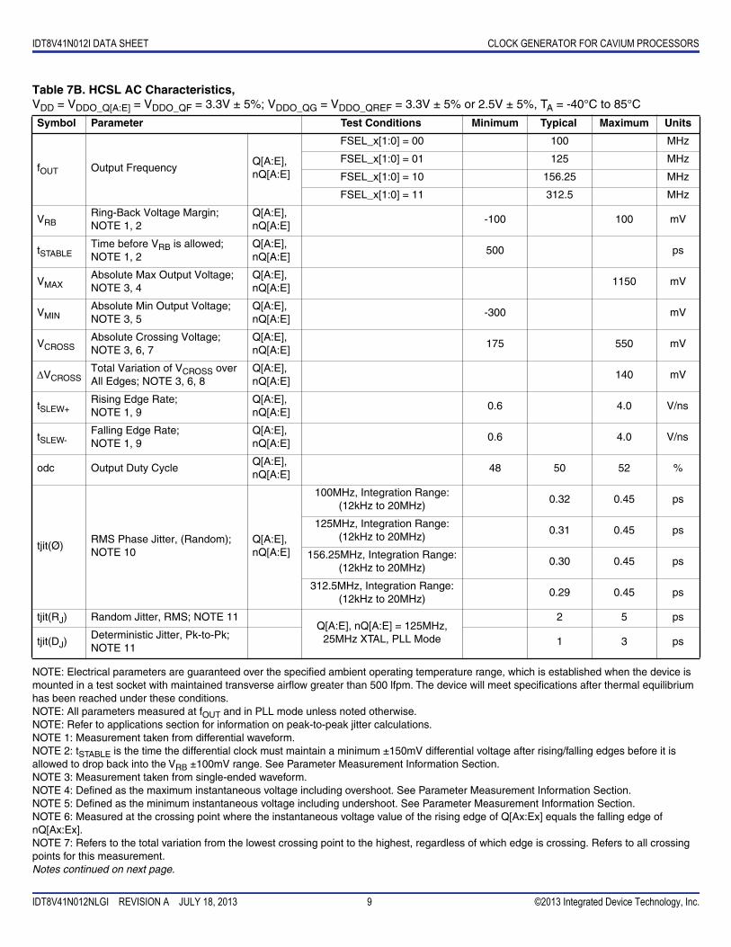
Table 7B. HCSL AC Characteristics,VDD = VDDO_Q[A:E] = VDDO_QF = 3.3V ± 5%; VDDO_QG = VDDO_QREF = 3.3V ± 5% or 2.5V ± 5%, TA = -40°C to 85°C
NOTE: Electrical parameters are guaranteed over the specified ambient operating temperature range, which is established when the device ismounted in a test socket with maintained transverse airflow greater than 500 lfpm. The device will meet specifications after thermal equilibriumhas been reached under these conditions.NOTE: All parameters measured at fOUT and in PLL mode unless noted otherwise.NOTE: Refer to applications section for information on peak-to-peak jitter calculations.NOTE 1: Measurement taken from differential waveform.NOTE 2: tSTABLE is the time the differential clock must maintain a minimum ±150mV differential voltage after rising/falling edges before it isallowed to drop back into the VRB ±100mV range. See Parameter Measurement Information Section.NOTE 3: Measurement taken from single-ended waveform.NOTE 4: Defined as the maximum instantaneous voltage including overshoot. See Parameter Measurement Information Section.NOTE 5: Defined as the minimum instantaneous voltage including undershoot. See Parameter Measurement Information Section.NOTE 6: Measured at the crossing point where the instantaneous voltage value of the rising edge of Q[Ax:Ex] equals the falling edge ofnQ[Ax:Ex].NOTE 7: Refers to the total variation from the lowest crossing point to the highest, regardless of which edge is crossing. Refers to all crossingpoints for this measurement.Notes continued on next page.
Symbol Parameter Test Conditions Minimum Typical Maximum Units
fOUT Output FrequencyQ[A:E],nQ[A:E]
FSEL_x[1:0] = 00 100 MHz
FSEL_x[1:0] = 01 125 MHz
FSEL_x[1:0] = 10 156.25 MHz
FSEL_x[1:0] = 11 312.5 MHz
VRBRing-Back Voltage Margin;NOTE 1, 2
Q[A:E],nQ[A:E]
-100 100 mV
tSTABLETime before VRB is allowed;NOTE 1, 2
Q[A:E],nQ[A:E]
500 ps
VMAXAbsolute Max Output Voltage;NOTE 3, 4
Q[A:E],nQ[A:E]
1150 mV
VMINAbsolute Min Output Voltage;NOTE 3, 5
Q[A:E],nQ[A:E]
-300 mV
VCROSSAbsolute Crossing Voltage;NOTE 3, 6, 7
Q[A:E],nQ[A:E]
175 550 mV
VCROSSTotal Variation of VCROSS overAll Edges; NOTE 3, 6, 8
Q[A:E],nQ[A:E]
140 mV
tSLEW+Rising Edge Rate;NOTE 1, 9
Q[A:E],nQ[A:E]
0.6 4.0 V/ns
tSLEW-Falling Edge Rate;NOTE 1, 9
Q[A:E],nQ[A:E]
0.6 4.0 V/ns
odc Output Duty CycleQ[A:E],nQ[A:E]
48 50 52 %
tjit(Ø)RMS Phase Jitter, (Random);NOTE 10
Q[A:E],nQ[A:E]
100MHz, Integration Range:(12kHz to 20MHz)
0.32 0.45 ps
125MHz, Integration Range:(12kHz to 20MHz)
0.31 0.45 ps
156.25MHz, Integration Range:(12kHz to 20MHz)
0.30 0.45 ps
312.5MHz, Integration Range:(12kHz to 20MHz)
0.29 0.45 ps
tjit(RJ) Random Jitter, RMS; NOTE 11Q[A:E], nQ[A:E] = 125MHz,
25MHz XTAL, PLL Mode
2 5 ps
tjit(DJ)Deterministic Jitter, Pk-to-Pk;NOTE 11
1 3 ps
IDT8V41N012I DATA SHEET CLOCK GENERATOR FOR CAVIUM PROCESSORS
IDT8V41N012NLGI REVISION A JULY 18, 2013 10 ©2013 Integrated Device Technology, Inc.
NOTE 8: Defined as the total variation of all crossing voltages of rising Q[Ax:Ex] and falling nQ[Ax:Ex]. This is the maximum allowed variance inVcross for any particular system.NOTE 9: Measured from -150mV to +150mV on the differential waveform (derived from Q[Ax:Ex] minus nQ[Ax:Ex]). The signal must bemonotonic through the measurement region for rise and fall time. The 300mV measurement window is centered on the differential zero crossing.NOTE 10: Measurements taken with 25MHz XTAL as input source and spur off.NOTE 11: Measurements taken with Wavecrest SIA-3000 Analyzer.
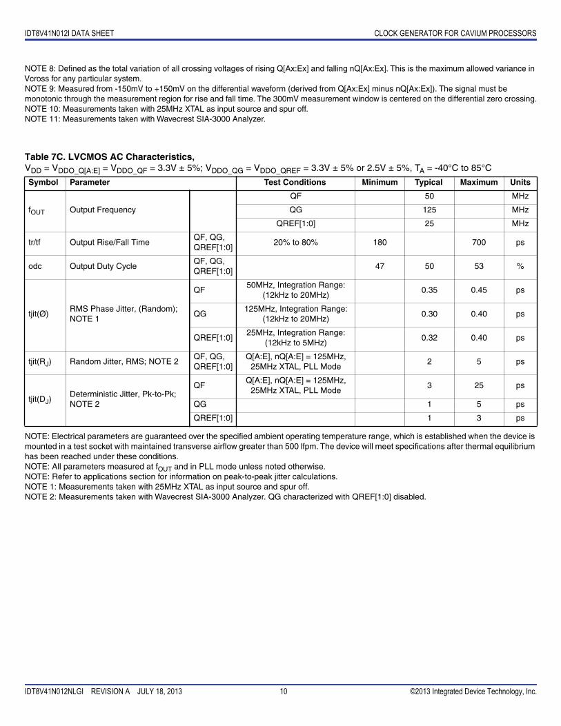
Table 7C. LVCMOS AC Characteristics,VDD = VDDO_Q[A:E] = VDDO_QF = 3.3V ± 5%; VDDO_QG = VDDO_QREF = 3.3V ± 5% or 2.5V ± 5%, TA = -40°C to 85°C
NOTE: Electrical parameters are guaranteed over the specified ambient operating temperature range, which is established when the device ismounted in a test socket with maintained transverse airflow greater than 500 lfpm. The device will meet specifications after thermal equilibriumhas been reached under these conditions.NOTE: All parameters measured at fOUT and in PLL mode unless noted otherwise.NOTE: Refer to applications section for information on peak-to-peak jitter calculations.NOTE 1: Measurements taken with 25MHz XTAL as input source and spur off.NOTE 2: Measurements taken with Wavecrest SIA-3000 Analyzer. QG characterized with QREF[1:0] disabled.
Symbol Parameter Test Conditions Minimum Typical Maximum Units
fOUT Output Frequency
QF 50 MHz
QG 125 MHz
QREF[1:0] 25 MHz
tr/tf Output Rise/Fall TimeQF, QG,QREF[1:0]
20% to 80% 180 700 ps
odc Output Duty CycleQF, QG,QREF[1:0]
47 50 53 %
tjit(Ø)RMS Phase Jitter, (Random);NOTE 1
QF50MHz, Integration Range:
(12kHz to 20MHz)0.35 0.45 ps
QG125MHz, Integration Range:
(12kHz to 20MHz)0.30 0.40 ps
QREF[1:0]25MHz, Integration Range:
(12kHz to 5MHz)0.32 0.40 ps
tjit(RJ) Random Jitter, RMS; NOTE 2QF, QG,QREF[1:0]
Q[A:E], nQ[A:E] = 125MHz,25MHz XTAL, PLL Mode
2 5 ps
tjit(DJ)Deterministic Jitter, Pk-to-Pk;NOTE 2
QFQ[A:E], nQ[A:E] = 125MHz,
25MHz XTAL, PLL Mode3 25 ps
QG 1 5 ps
QREF[1:0] 1 3 ps
IDT8V41N012I DATA SHEET CLOCK GENERATOR FOR CAVIUM PROCESSORS
IDT8V41N012NLGI REVISION A JULY 18, 2013 11 ©2013 Integrated Device Technology, Inc.
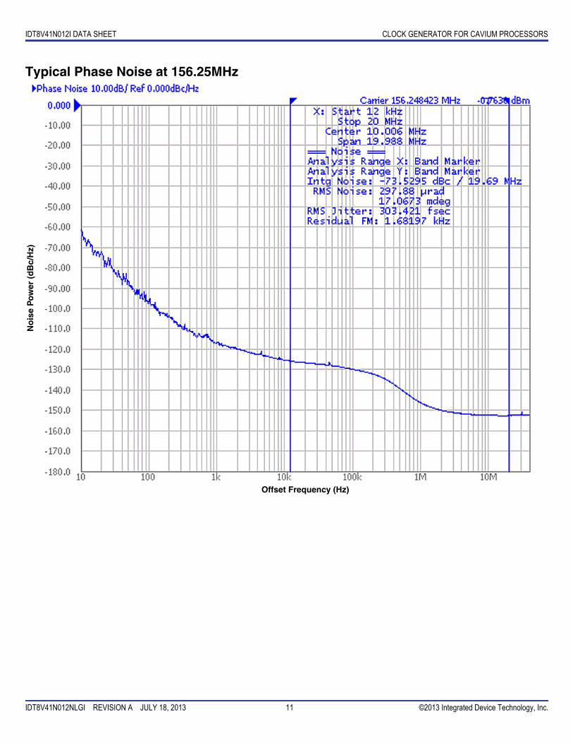
Typical Phase Noise at 156.25MHz
No
ise
Po
wer
(dB
c/H
z)
Offset Frequency (Hz)
IDT8V41N012I DATA SHEET CLOCK GENERATOR FOR CAVIUM PROCESSORS
IDT8V41N012NLGI REVISION A JULY 18, 2013 12 ©2013 Integrated Device Technology, Inc.
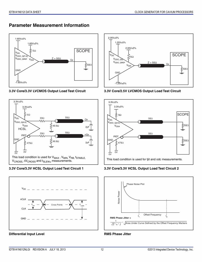
Parameter Measurement Information
3.3V Core/3.3V LVCMOS Output Load Test Circuit
3.3V Core/3.3V HCSL Output Load Test Circuit 1
Differential Input Level
3.3V Core/2.5V LVCMOS Output Load Test Circuit
3.3V Core/3.3V HCSL Output Load Test Circuit 2
RMS Phase Jitter
SCOPE
Qx
GND
-1.65V±5%
VDDO_Q[F:G],
1.65V±5%
VDD,
VDDA
1.65V±5%
VDDO_QREF
VDD,
3.3V±5%
3.3V±5%
VDDA
VDDO_Q[A:E]
This load condition is used for VMAX , VMIN, VRB, tSTABLE,VCROSS, VCROSS and tSLEW± measurements.
nCLK
CLK
VDD
GND
VCMR
Cross PointsVPP
SCOPE
Qx
GND
-1.25V±5%
2.05V±5%
1.25V±5%
VDD
VDDA
2.05V±5%
VDDO_QG,VDDO_QREF
This load condition is used for tjit and odc measurements.
475
50
50
GND
0V
SCOPE
IREF
0V
3.3V±5%
3.3V±5%
VDD,VDDO_Q[A:E]
VDDA
IDT8V41N012I DATA SHEET CLOCK GENERATOR FOR CAVIUM PROCESSORS
IDT8V41N012NLGI REVISION A JULY 18, 2013 13 ©2013 Integrated Device Technology, Inc.
Parameter Measurement Information, continued
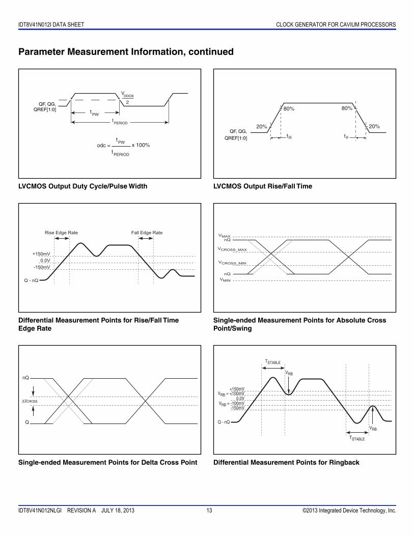
LVCMOS Output Duty Cycle/Pulse Width
Differential Measurement Points for Rise/Fall TimeEdge Rate
Single-ended Measurement Points for Delta Cross Point
LVCMOS Output Rise/Fall Time
Single-ended Measurement Points for Absolute CrossPoint/Swing
Differential Measurement Points for Ringback
QF, QG,QREF[1:0]
20%
80% 80%
20%
tR tF
QF, QG,QREF[1:0]
IDT8V41N012I DATA SHEET CLOCK GENERATOR FOR CAVIUM PROCESSORS
IDT8V41N012NLGI REVISION A JULY 18, 2013 14 ©2013 Integrated Device Technology, Inc.
Parameter Measurement Information, continued
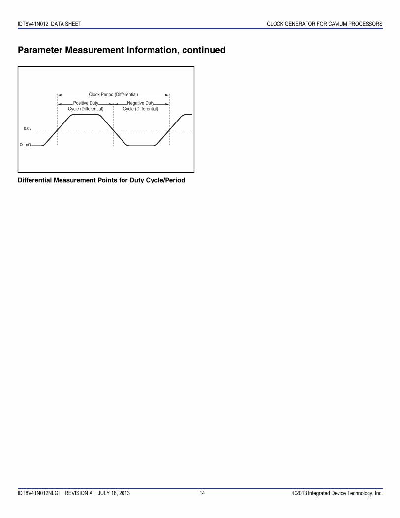
Differential Measurement Points for Duty Cycle/Period
IDT8V41N012I DATA SHEET CLOCK GENERATOR FOR CAVIUM PROCESSORS
IDT8V41N012NLGI REVISION A JULY 18, 2013 15 ©2013 Integrated Device Technology, Inc.
Applications Information
Peak-to-Peak Jitter Calculations
A standard deviation of a statistical population or data set is thesquare root of its variance. A standard deviation is used to calculatethe probability of an anomaly or to predict a failure. Many times, theterm "root mean square" (RMS) is used synonymously for standarddeviation. This is accurate when referring to the square root of themean squared deviation of a signal from a given baseline and whenthe data set contains a Gaussian distribution with no deterministiccomponents. A low standard deviation indicates that the data set isclose to the mean with little variation. A large standard deviationindicates that the data set is spread out and has a large variation fromthe mean.
A standard deviation is required when calculating peak-to-peak jitter.Since true peak-to-peak jitter is random and unbounded, it isimportant to always associate a bit error ratio (BER) when specifyinga peak-to-peak jitter limit. Without it, the specification does not havea boundary and will continue get larger with sample size. Given thata BER is application specific, many frequency timing devices specifyjitter as an RMS. This allows the peak-to-peak jitter to be calculatedfor the specific application and BER requirement. Because astandard deviation is the variation from the mean of the data set, it isimportant to always calculate the peak-to-peak jitter using the typicalRMS value.
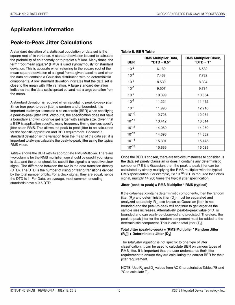
Table 8 shows the BER with its appropriate RMS Multiplier. There aretwo columns for the RMS multiplier, one should be used if your signalis data and the other should be used if the signal is a repetitive clocksignal. The difference between the two is the data transition density(DTD). The DTD is the number of rising or falling transitions dividedby the total number of bits. For a clock signal, they are equal, hencethe DTD is 1. For Data, on average, most common encodingstandards have a 0.5 DTD.
Table 8. BER Table
Once the BER is chosen, there are two circumstances to consider. Isthe data set purely Gaussian or does it contains any deterministiccomponent? If it is Gaussian, then the peak to peak jitter can becalculated by simply multiplying the RMS multiplier with the typicalRMS specification. For example, if a 10-12 BER is required for a clocksignal, multiply 14.260 times the typical jitter specification.
Jitter (peak-to-peak) = RMS Multiplier * RMS (typical)
If the datasheet contains deterministic components, then the randomjitter (RJ) and deterministic jitter (DJ) must be separated andanalyzed separately. RJ, also known as Gaussian jitter, is notbounded and the peak-to-peak will continue to get larger as thesample size increases. Alternatively, peak-to-peak value of DJ isbounded and can easily be observed and predicted. Therefore, thepeak to peak jitter for the random component must be added to thedeterministic component. This is called total jitter (TJ).
Total Jitter (peak-to-peak) = [RMS Multiplier * Random Jitter(RJ)] + Deterministic Jitter (DJ)
The total jitter equation is not specific to one type of jitterclassification. It can be used to calculate BER on various types ofRMS jitter. It is important that the user understands their jitterrequirement to ensure they are calculating the correct BER for theirjitter requirement.
NOTE: Use RJ and DJ values from AC Characteristics Tables 7B and7C to calculate TJ.
BERRMS Multiplier Data,
“DTD = 0.5”RMS Multiplier Clock,
“DTD = 1”
10-3 6.180 6.582
10-4 7.438 7.782
10-5 8.530 8.834
10-6 9.507 9.784
10-7 10.399 10.654
10-8 11.224 11.462
10-9 11.996 12.218
10-10 12.723 12.934
10-11 13.412 13.614
10-12 14.069 14.260
10-13 14.698 14.882
10-14 15.301 15.478
10-15 15.883 16.028
IDT8V41N012I DATA SHEET CLOCK GENERATOR FOR CAVIUM PROCESSORS
IDT8V41N012NLGI REVISION A JULY 18, 2013 16 ©2013 Integrated Device Technology, Inc.
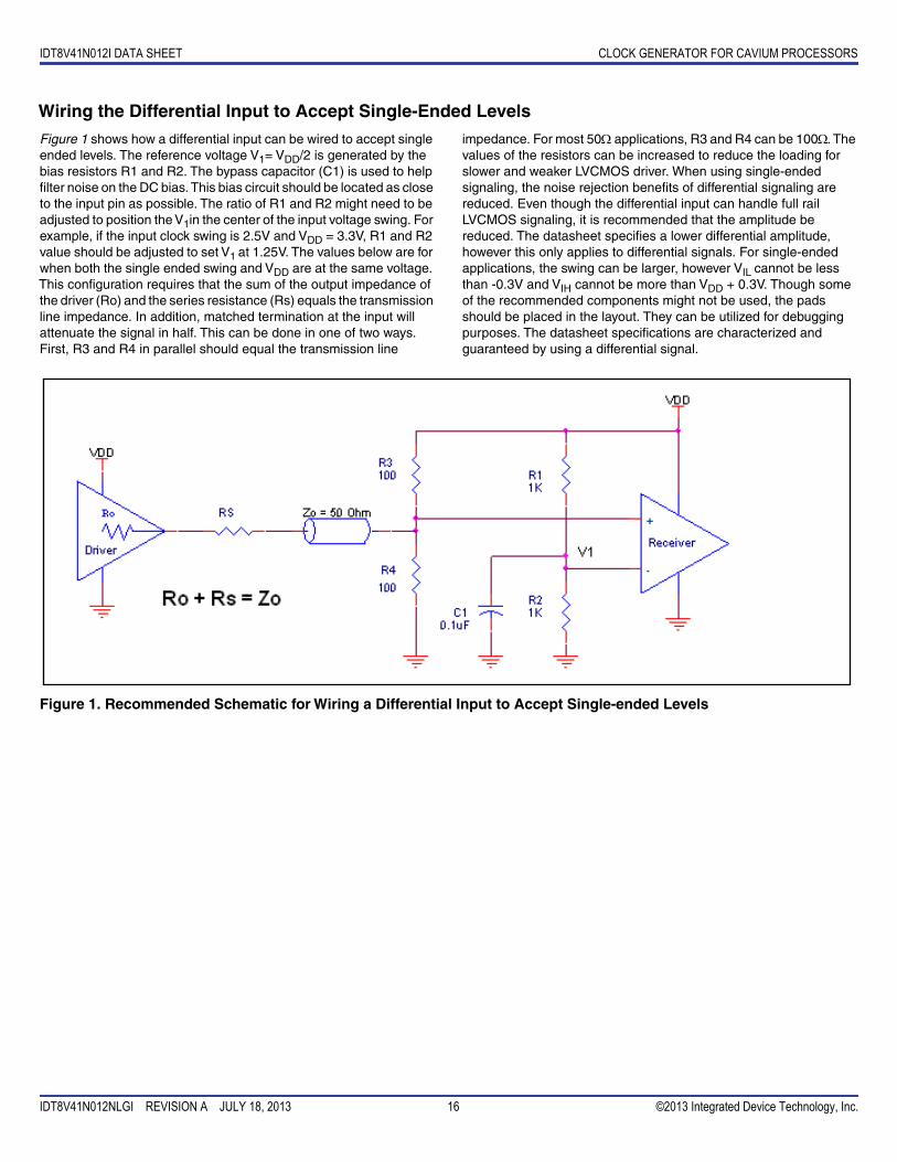
Wiring the Differential Input to Accept Single-Ended Levels
Figure 1 shows how a differential input can be wired to accept singleended levels. The reference voltage V1= VDD/2 is generated by thebias resistors R1 and R2. The bypass capacitor (C1) is used to helpfilter noise on the DC bias. This bias circuit should be located as closeto the input pin as possible. The ratio of R1 and R2 might need to beadjusted to position the V1in the center of the input voltage swing. Forexample, if the input clock swing is 2.5V and VDD = 3.3V, R1 and R2value should be adjusted to set V1 at 1.25V. The values below are forwhen both the single ended swing and VDD are at the same voltage.This configuration requires that the sum of the output impedance ofthe driver (Ro) and the series resistance (Rs) equals the transmissionline impedance. In addition, matched termination at the input willattenuate the signal in half. This can be done in one of two ways.First, R3 and R4 in parallel should equal the transmission line
impedance. For most 50 applications, R3 and R4 can be 100. Thevalues of the resistors can be increased to reduce the loading forslower and weaker LVCMOS driver. When using single-endedsignaling, the noise rejection benefits of differential signaling arereduced. Even though the differential input can handle full railLVCMOS signaling, it is recommended that the amplitude bereduced. The datasheet specifies a lower differential amplitude,however this only applies to differential signals. For single-endedapplications, the swing can be larger, however VIL cannot be lessthan -0.3V and VIH cannot be more than VDD + 0.3V. Though someof the recommended components might not be used, the padsshould be placed in the layout. They can be utilized for debuggingpurposes. The datasheet specifications are characterized andguaranteed by using a differential signal.
Figure 1. Recommended Schematic for Wiring a Differential Input to Accept Single-ended Levels
IDT8V41N012I DATA SHEET CLOCK GENERATOR FOR CAVIUM PROCESSORS
IDT8V41N012NLGI REVISION A JULY 18, 2013 17 ©2013 Integrated Device Technology, Inc.
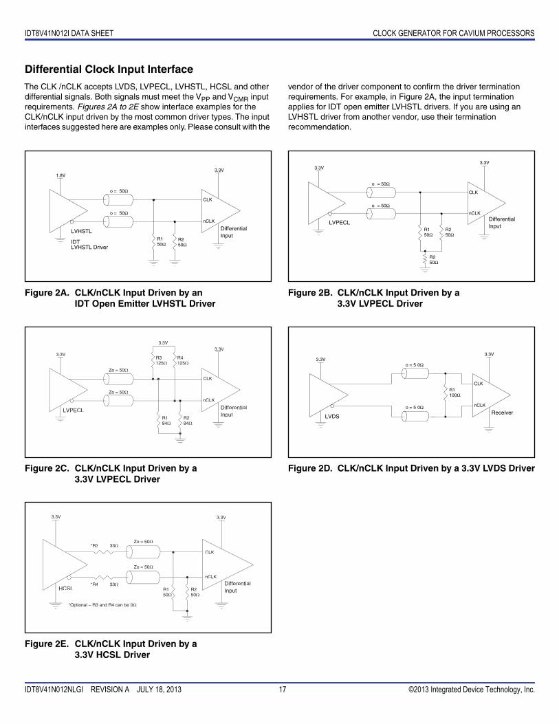
Differential Clock Input Interface
The CLK /nCLK accepts LVDS, LVPECL, LVHSTL, HCSL and otherdifferential signals. Both signals must meet the VPP and VCMR inputrequirements. Figures 2A to 2E show interface examples for theCLK/nCLK input driven by the most common driver types. The inputinterfaces suggested here are examples only. Please consult with the
vendor of the driver component to confirm the driver terminationrequirements. For example, in Figure 2A, the input terminationapplies for IDT open emitter LVHSTL drivers. If you are using anLVHSTL driver from another vendor, use their terminationrecommendation.
Figure 2A. CLK/nCLK Input Driven by anIDT Open Emitter LVHSTL Driver
Figure 2C. CLK/nCLK Input Driven by a3.3V LVPECL Driver
Figure 2E. CLK/nCLK Input Driven by a3.3V HCSL Driver
Figure 2B. CLK/nCLK Input Driven by a3.3V LVPECL Driver
Figure 2D. CLK/nCLK Input Driven by a 3.3V LVDS Driver
R150Ω
R250Ω
1.8V
o = 50Ω
o = 50Ω
CLK
nCLK
3.3V
LVHSTL
IDTLVHSTL Driver
DifferentialInput
3.3V
CLK
nCLK
3.3V3.3V
LVPECL DifferentialInput
HCSL
*R3
*R4
CLK
nCLK
3.3V 3.3V
DifferentialInput
CLK
nCLKDifferentialInput
LVPECL
3.3V
o = 50Ω
o = 50Ω
3.3V
R150Ω
R250Ω
R250Ω
3.3V
R1100Ω
LVDS
CLK
nCLK
3.3V
Receiver
o = 5 0Ω
o = 5 0Ω
IDT8V41N012I DATA SHEET CLOCK GENERATOR FOR CAVIUM PROCESSORS
IDT8V41N012NLGI REVISION A JULY 18, 2013 18 ©2013 Integrated Device Technology, Inc.
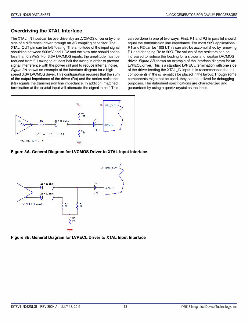
Overdriving the XTAL Interface
The XTAL_IN input can be overdriven by an LVCMOS driver or by oneside of a differential driver through an AC coupling capacitor. TheXTAL_OUT pin can be left floating. The amplitude of the input signalshould be between 500mV and 1.8V and the slew rate should not beless than 0.2V/nS. For 3.3V LVCMOS inputs, the amplitude must bereduced from full swing to at least half the swing in order to preventsignal interference with the power rail and to reduce internal noise.Figure 3A shows an example of the interface diagram for a highspeed 3.3V LVCMOS driver. This configuration requires that the sumof the output impedance of the driver (Ro) and the series resistance(Rs) equals the transmission line impedance. In addition, matchedtermination at the crystal input will attenuate the signal in half. This
can be done in one of two ways. First, R1 and R2 in parallel shouldequal the transmission line impedance. For most 50 applications,R1 and R2 can be 100. This can also be accomplished by removingR1 and changing R2 to 50. The values of the resistors can beincreased to reduce the loading for a slower and weaker LVCMOSdriver. Figure 3B shows an example of the interface diagram for anLVPECL driver. This is a standard LVPECL termination with one sideof the driver feeding the XTAL_IN input. It is recommended that allcomponents in the schematics be placed in the layout. Though somecomponents might not be used, they can be utilized for debuggingpurposes. The datasheet specifications are characterized andguaranteed by using a quartz crystal as the input.
Figure 3A. General Diagram for LVCMOS Driver to XTAL Input Interface
Figure 3B. General Diagram for LVPECL Driver to XTAL Input Interface
IDT8V41N012I DATA SHEET CLOCK GENERATOR FOR CAVIUM PROCESSORS
IDT8V41N012NLGI REVISION A JULY 18, 2013 19 ©2013 Integrated Device Technology, Inc.
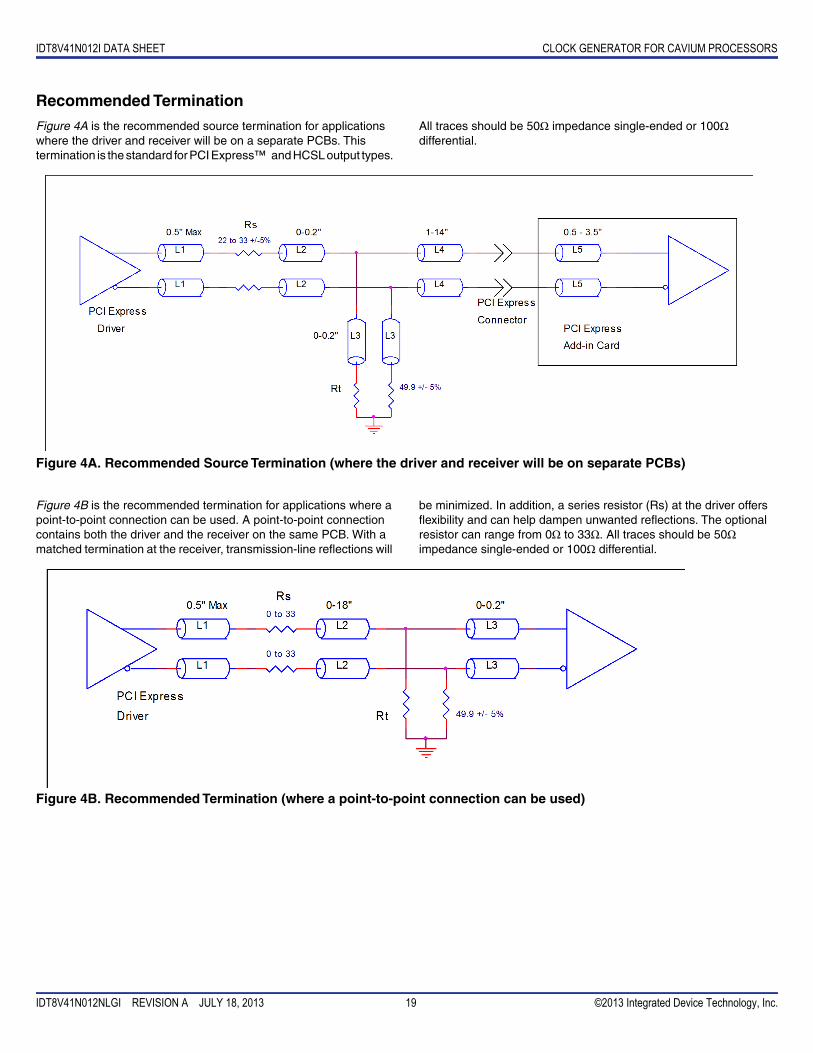
Recommended Termination
Figure 4A is the recommended source termination for applicationswhere the driver and receiver will be on a separate PCBs. Thistermination is the standard for PCI Express™ and HCSL output types.
All traces should be 50Ω impedance single-ended or 100Ωdifferential.
Figure 4A. Recommended Source Termination (where the driver and receiver will be on separate PCBs)
Figure 4B is the recommended termination for applications where apoint-to-point connection can be used. A point-to-point connectioncontains both the driver and the receiver on the same PCB. With amatched termination at the receiver, transmission-line reflections will
be minimized. In addition, a series resistor (Rs) at the driver offersflexibility and can help dampen unwanted reflections. The optionalresistor can range from 0Ω to 33Ω. All traces should be 50Ωimpedance single-ended or 100Ω differential.
Figure 4B. Recommended Termination (where a point-to-point connection can be used)
IDT8V41N012I DATA SHEET CLOCK GENERATOR FOR CAVIUM PROCESSORS
IDT8V41N012NLGI REVISION A JULY 18, 2013 20 ©2013 Integrated Device Technology, Inc.
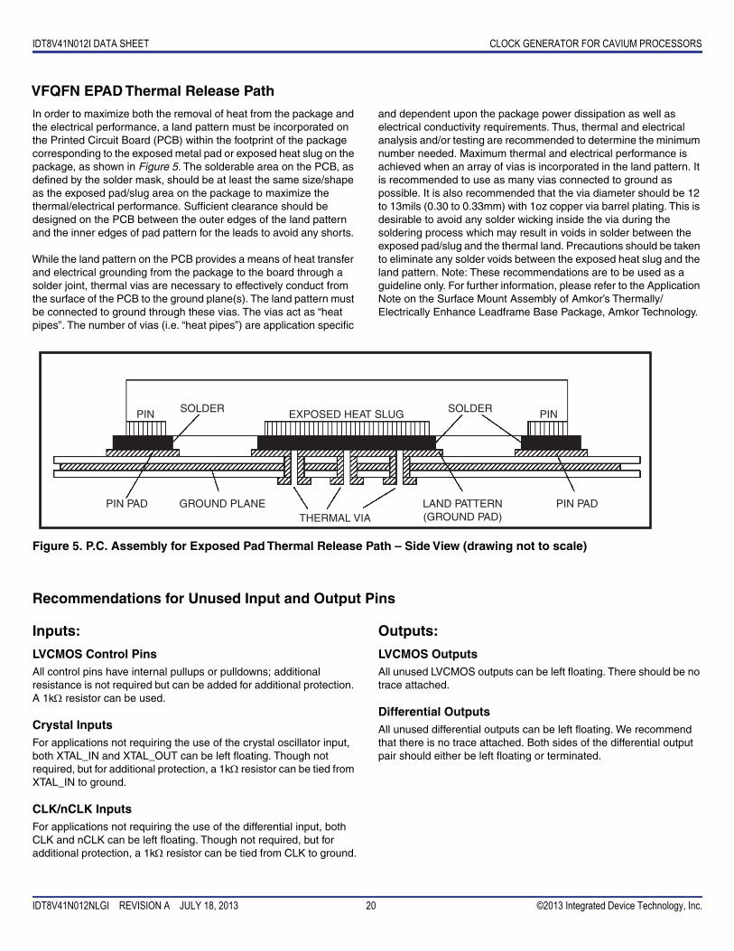
VFQFN EPAD Thermal Release Path
In order to maximize both the removal of heat from the package andthe electrical performance, a land pattern must be incorporated onthe Printed Circuit Board (PCB) within the footprint of the packagecorresponding to the exposed metal pad or exposed heat slug on thepackage, as shown in Figure 5. The solderable area on the PCB, asdefined by the solder mask, should be at least the same size/shapeas the exposed pad/slug area on the package to maximize thethermal/electrical performance. Sufficient clearance should bedesigned on the PCB between the outer edges of the land patternand the inner edges of pad pattern for the leads to avoid any shorts.
While the land pattern on the PCB provides a means of heat transferand electrical grounding from the package to the board through asolder joint, thermal vias are necessary to effectively conduct fromthe surface of the PCB to the ground plane(s). The land pattern mustbe connected to ground through these vias. The vias act as “heatpipes”. The number of vias (i.e. “heat pipes”) are application specific
and dependent upon the package power dissipation as well aselectrical conductivity requirements. Thus, thermal and electricalanalysis and/or testing are recommended to determine the minimumnumber needed. Maximum thermal and electrical performance isachieved when an array of vias is incorporated in the land pattern. Itis recommended to use as many vias connected to ground aspossible. It is also recommended that the via diameter should be 12to 13mils (0.30 to 0.33mm) with 1oz copper via barrel plating. This isdesirable to avoid any solder wicking inside the via during thesoldering process which may result in voids in solder between theexposed pad/slug and the thermal land. Precautions should be takento eliminate any solder voids between the exposed heat slug and theland pattern. Note: These recommendations are to be used as aguideline only. For further information, please refer to the ApplicationNote on the Surface Mount Assembly of Amkor’s Thermally/Electrically Enhance Leadframe Base Package, Amkor Technology.
Figure 5. P.C. Assembly for Exposed Pad Thermal Release Path – Side View (drawing not to scale)
Recommendations for Unused Input and Output Pins
Inputs:
LVCMOS Control PinsAll control pins have internal pullups or pulldowns; additionalresistance is not required but can be added for additional protection.A 1k resistor can be used.
Crystal InputsFor applications not requiring the use of the crystal oscillator input,both XTAL_IN and XTAL_OUT can be left floating. Though notrequired, but for additional protection, a 1k resistor can be tied fromXTAL_IN to ground.
CLK/nCLK InputsFor applications not requiring the use of the differential input, bothCLK and nCLK can be left floating. Though not required, but foradditional protection, a 1k resistor can be tied from CLK to ground.
Outputs:
LVCMOS OutputsAll unused LVCMOS outputs can be left floating. There should be notrace attached.
Differential OutputsAll unused differential outputs can be left floating. We recommendthat there is no trace attached. Both sides of the differential outputpair should either be left floating or terminated.
SOLDERSOLDER PINPIN EXPOSED HEAT SLUG
PIN PAD PIN PADGROUND PLANE LAND PATTERN(GROUND PAD)THERMAL VIA
IDT8V41N012I DATA SHEET CLOCK GENERATOR FOR CAVIUM PROCESSORS
IDT8V41N012NLGI REVISION A JULY 18, 2013 21 ©2013 Integrated Device Technology, Inc.
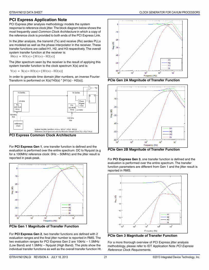
PCI Express Application NotePCI Express jitter analysis methodology models the systemresponse to reference clock jitter. The block diagram below shows themost frequently used Common Clock Architecture in which a copy ofthe reference clock is provided to both ends of the PCI Express Link.
In the jitter analysis, the transmit (Tx) and receive (Rx) serdes PLLsare modeled as well as the phase interpolator in the receiver. Thesetransfer functions are called H1, H2, and H3 respectively. The overallsystem transfer function at the receiver is:
The jitter spectrum seen by the receiver is the result of applying thissystem transfer function to the clock spectrum X(s) and is:
In order to generate time domain jitter numbers, an inverse FourierTransform is performed on X(s)*H3(s) * [H1(s) - H2(s)].
PCI Express Common Clock Architecture
For PCI Express Gen 1, one transfer function is defined and theevaluation is performed over the entire spectrum: DC to Nyquist (e.gfor a 100MHz reference clock: 0Hz – 50MHz) and the jitter result isreported in peak-peak.
PCIe Gen 1 Magnitude of Transfer Function
For PCI Express Gen 2, two transfer functions are defined with 2evaluation ranges and the final jitter number is reported in RMS. Thetwo evaluation ranges for PCI Express Gen 2 are 10kHz – 1.5MHz(Low Band) and 1.5MHz – Nyquist (High Band). The plots show theindividual transfer functions as well as the overall transfer function Ht.
PCIe Gen 2A Magnitude of Transfer Function
PCIe Gen 2B Magnitude of Transfer Function
For PCI Express Gen 3, one transfer function is defined and theevaluation is performed over the entire spectrum. The transferfunction parameters are different from Gen 1 and the jitter result isreported in RMS.
PCIe Gen 3 Magnitude of Transfer Function
For a more thorough overview of PCI Express jitter analysismethodology, please refer to IDT Application Note PCI ExpressReference Clock Requirements.
Ht s H3 s H1 s H2 s – =
Y s X s H3 s H1 s H2 s – =
IDT8V41N012I DATA SHEET CLOCK GENERATOR FOR CAVIUM PROCESSORS
IDT8V41N012NLGI REVISION A JULY 18, 2013 22 ©2013 Integrated Device Technology, Inc.
Schematic Example
Figure 6 (next page) shows an example of IDT8V41N012I applicationschematic. In this example, the device is operated at VDD = VDDA =VDDO_Qx = 3.3V. The schematic example focuses on functionalconnections and is not configuration specific. Refer to the pindescription and functional tables in the datasheet to ensure that thelogic control inputs are properly set.
A 12pF parallel resonant 25MHz crystal is used. For this device, thecrystal load capacitors are required for proper operation. The loadcapacitance, C1 = C2 = 2pF, are recommended for frequencyaccuracy. Depending on the variation of the parasitic stray capacityof the printed circuit board traces between the crystal and the Xtal_Inand Xtal_Out pins, the values of C1 and C2 might require a slightadjustment to optimize the frequency accuracy. Crystals with otherload capacitance specifications can be used, but this will requireadjusting C1 and C2. When designing the circuit board, return thecapacitors to ground though a single point contact close to thepackage. Two Fox crystal options are shown in the schematic fordesign flexibility.
The ePAD provides a low thermal impedance connection betweenthe internal device and the PCB. It also provides an electricalconnection to the die and must be connected to ground.
As with any high speed analog circuitry, the power supply pins arevulnerable to random noise. To achieve optimum jitter performance,power supply isolation is required. The IDT8V41N012I providesseparate power supplies to isolate any high switching noise fromcoupling into the internal PLL.
In order to achieve the best possible filtering, it is recommended thatthe placement of the filter components be on the device side of thePCB as close to the power pins as possible. If space is limited, the0.1µF capacitor in each power pin filter should be placed on thedevice side. The other components can be on the opposite side of thePCB.
Power supply filter recommendations are a general guideline to beused for reducing external noise from coupling into the devices. Thefilter performance is designed for a wide range of noise frequencies.This low-pass filter starts to attenuate noise at approximately 10kHz.If a specific frequency noise component is known, such as switchingpower supplies frequencies, it is recommended that componentvalues be adjusted and if required, additional filtering be added.Additionally, good general design practices for power plane voltagestability suggests adding bulk capacitance in the local area of alldevices.

IDT8V41N012I DATA SHEET CLOCK GENERATOR FOR CAVIUM PROCESSORS
IDT8V41N012NLGI REVISION A JULY 18, 2013 23 ©2013 Integrated Device Technology, Inc.
Figure 6. IDT8V41N012I Schematic Example
IDT8V41N012I DATA SHEET CLOCK GENERATOR FOR CAVIUM PROCESSORS
IDT8V41N012NLGI REVISION A JULY 18, 2013 24 ©2013 Integrated Device Technology, Inc.
Power ConsiderationsThis section provides information on power dissipation and junction temperature for the IDT8V41N012I. Equations and example calculationsare also provided.
1. Power Dissipation.
The total power dissipation for the IDT8V41N012I is the sum of the core power plus the analog power plus the power dissipated due to loading.The following is the power dissipation for VDD = 3.3V + 5% = 3.465V, which gives worst case results.
NOTE: Please refer to Section 3 for details on calculating power dissipated due to loading.
• Power (core)MAX = VDD_MAX * (IDD + IDDA)= 3.465V * (235mA + 45mA) = 970.2mW
• Power (HCSL)MAX = (3.465V – 17mA * 50) 17mA = 44.5mW per output
• Total Power (HCSL)MAX = 44.5mW * 10 = 445mW
LVCMOS Driver Power Dissipation
• Output Impedance ROUT Power Dissipation due to Loading 50 to VDDO_Qx / 2Output Current IOUT = VDD_MAX / [2 * (50 + ROUT)] = 3.465V / [2 * (50 + 15)] = 26.65mA
• Power Dissipation on the ROUT per LVCMOS outputPower (LVCMOS) = ROUT * (IOUT)2 = 15 * (26.65mA)2 = 10.65mW per output
• Total Power Dissipation on the ROUTTotal Power (ROUT) = 10.65mW * 4 = 42.6mW
• Total Power Dissipation• Total Power
= Power (core) + Total Power (HCSL) + Total Power (ROUT)= 970.2mW + 445mW + 42.6mW= 1457.8mW
2. Junction Temperature.
Junction temperature, Tj, is the temperature at the junction of the bond wire and bond pad directly affects the reliability of the device. Themaximum recommended junction temperature is 125°C. Limiting the internal transistor junction temperature, Tj, to 125°C ensures that the bondwire and bond pad temperature remains below 125°C.
The equation for Tj is as follows: Tj = JA * Pd_total + TA
Tj = Junction Temperature
JA = Junction-to-Ambient Thermal Resistance
Pd_total = Total Device Power Dissipation (example calculation is in section 1 above)
TA = Ambient Temperature
In order to calculate junction temperature, the appropriate junction-to-ambient thermal resistance JA must be used. Assuming no air flow anda multi-layer board, the appropriate value is 26.6°C/W per Table 9 below.
Therefore, Tj for an ambient temperature of 85°C with all outputs switching is:
85°C + 1.458W * 26.6°C/W = 123.8°C. This is below the limit of 125°C.
This calculation is only an example. Tj will obviously vary depending on the number of loaded outputs, supply voltage, air flow and the type ofboard (multi-layer).
Table 9. Thermal Resistance JA for 72 Lead VFQFN, Forced Convection
JA vs. Air Flow
Meters per Second 0 1 2
Multi-Layer PCB, JEDEC Standard Test Boards 26.6°C/W 20°C/W 17.9°C/W
IDT8V41N012I DATA SHEET CLOCK GENERATOR FOR CAVIUM PROCESSORS
IDT8V41N012NLGI REVISION A JULY 18, 2013 25 ©2013 Integrated Device Technology, Inc.
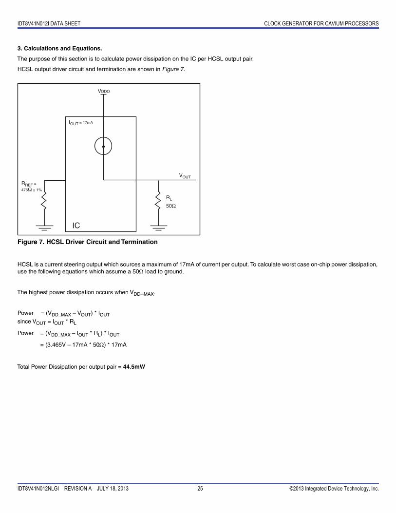
3. Calculations and Equations.
The purpose of this section is to calculate power dissipation on the IC per HCSL output pair.
HCSL output driver circuit and termination are shown in Figure 7.
Figure 7. HCSL Driver Circuit and Termination
HCSL is a current steering output which sources a maximum of 17mA of current per output. To calculate worst case on-chip power dissipation,use the following equations which assume a 50 load to ground.
The highest power dissipation occurs when VDD_MAX.
Power = (VDD_MAX – VOUT) * IOUT
since VOUT = IOUT * RL
Power = (VDD_MAX – IOUT * RL) * IOUT
= (3.465V – 17mA * 50) * 17mA
Total Power Dissipation per output pair = 44.5mW
VDDO
VOUT
RL
50Ω
IC
➤
IOUT = 17mA
RREF =
475Ω ± 1%
IDT8V41N012I DATA SHEET CLOCK GENERATOR FOR CAVIUM PROCESSORS
IDT8V41N012NLGI REVISION A JULY 18, 2013 26 ©2013 Integrated Device Technology, Inc.
Reliability InformationTable 10. JA vs. Air Flow Table for a 72 Lead VFQFN
Transistor CountThe transistor count for IDT8V41N012I is: 175,936
JA vs. Air Flow
Meters per Second 0 1 2
Multi-Layer PCB, JEDEC Standard Test Boards 26.6°C/W 20°C/W 17.9°C/W
IDT8V41N012I DATA SHEET CLOCK GENERATOR FOR CAVIUM PROCESSORS
IDT8V41N012NLGI REVISION A JULY 18, 2013 27 ©2013 Integrated Device Technology, Inc.
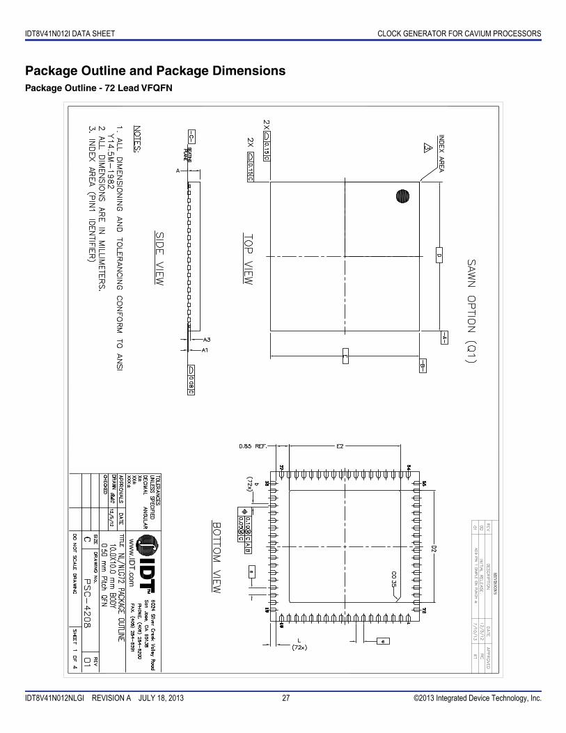
Package Outline and Package DimensionsPackage Outline - 72 Lead VFQFN
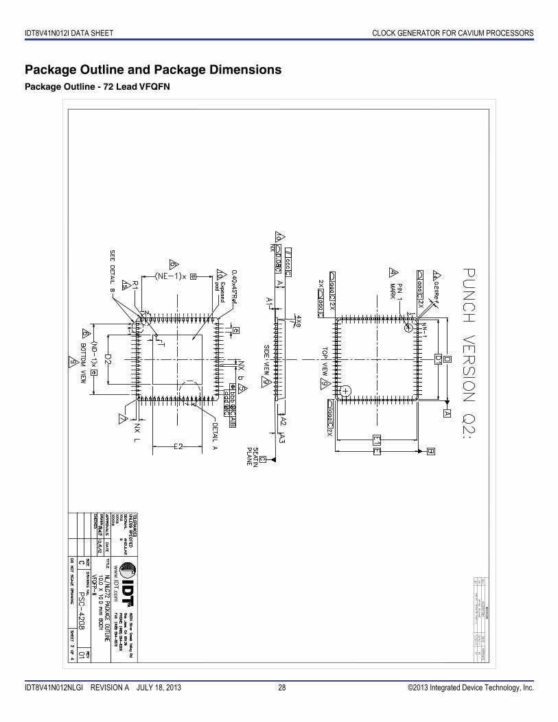
IDT8V41N012I DATA SHEET CLOCK GENERATOR FOR CAVIUM PROCESSORS
IDT8V41N012NLGI REVISION A JULY 18, 2013 28 ©2013 Integrated Device Technology, Inc.
Package Outline and Package DimensionsPackage Outline - 72 Lead VFQFN
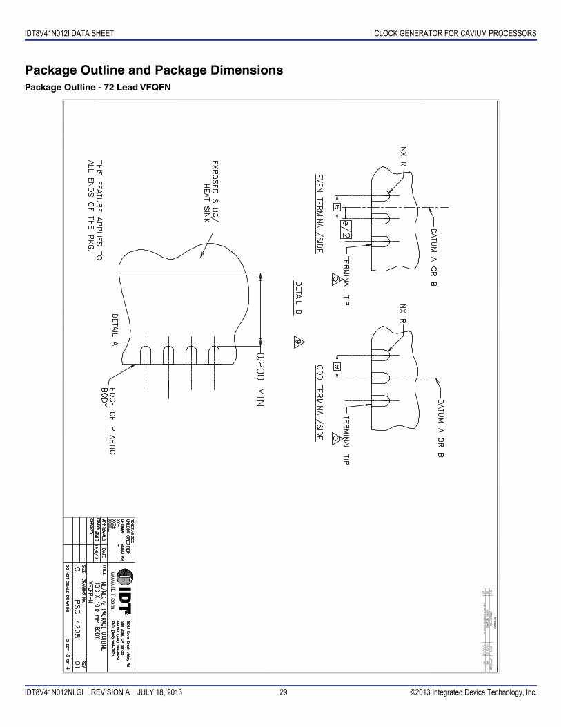
IDT8V41N012I DATA SHEET CLOCK GENERATOR FOR CAVIUM PROCESSORS
IDT8V41N012NLGI REVISION A JULY 18, 2013 29 ©2013 Integrated Device Technology, Inc.
Package Outline and Package DimensionsPackage Outline - 72 Lead VFQFN
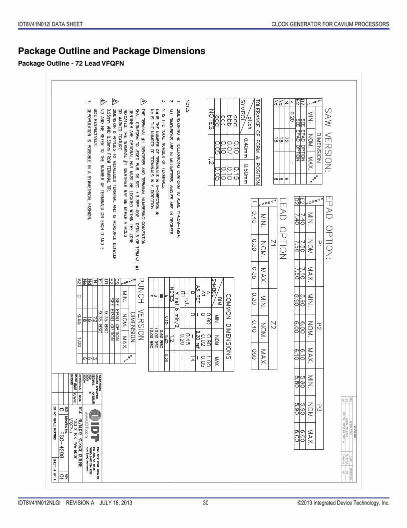
IDT8V41N012I DATA SHEET CLOCK GENERATOR FOR CAVIUM PROCESSORS
IDT8V41N012NLGI REVISION A JULY 18, 2013 30 ©2013 Integrated Device Technology, Inc.
Package Outline and Package DimensionsPackage Outline - 72 Lead VFQFN
IDT8V41N012I DATA SHEET CLOCK GENERATOR FOR CAVIUM PROCESSORS
IDT8V41N012NLGI REVISION A JULY 18, 2013 31 ©2013 Integrated Device Technology, Inc.
Ordering InformationTable 11. Ordering Information
Part/Order Number Marking Package Shipping Packaging Temperature8V41N012NLGI 8V41N012NLGI Lead-Free, 72 Lead VFQFN Tray -40C to 85C8V41N012NLGI8 8V41N012NLGI Lead-Free, 72 Lead VFQFN Tape & Reel -40C to 85C
DISCLAIMER Integrated Device Technology, Inc. (IDT) and its subsidiaries reserve the right to modify the products and/or specifications described herein at any time and at IDT’s sole discretion. All information in this document,including descriptions of product features and performance, is subject to change without notice. Performance specifications and the operating parameters of the described products are determined in the independent state and are notguaranteed to perform the same way when installed in customer products. The information contained herein is provided without representation or warranty of any kind, whether express or implied, including, but not limited to, thesuitability of IDT’s products for any particular purpose, an implied warranty of merchantability, or non-infringement of the intellectual property rights of others. This document is presented only as a guide and does not convey anylicense under intellectual property rights of IDT or any third parties.
IDT’s products are not intended for use in applications involving extreme environmental conditions or in life support systems or similar devices where the failure or malfunction of an IDT product can be reasonably expected to signifi-cantly affect the health or safety of users. Anyone using an IDT product in such a manner does so at their own risk, absent an express, written agreement by IDT.
Integrated Device Technology, IDT and the IDT logo are registered trademarks of IDT. Other trademarks and service marks used herein, including protected names, logos and designs, are the property of IDT or their respective thirdparty owners.
Copyright 2013. All rights reserved.
6024 Silver Creek Valley Road San Jose, California 95138
Sales800-345-7015 (inside USA)+408-284-8200 (outside USA)Fax: 408-284-2775www.IDT.com/go/contactIDT
Technical Support [email protected]+480-763-2056
We’ve Got Your Timing Solution
IDT8V41N012I DATA SHEET CLOCK GENERATOR FOR CAVIUM PROCESSORS


![Runtime Power Monitoring in High-End Processors ...mrmgroup.cs.princeton.edu/papers/canturkmicro.pdf · cessor clock cycle [11, 26]. Intel P4 performance monitor-ing events comprise](https://img.dokumen.tips/doc/110x75/5f72dfbb9bda797fc5383856/runtime-power-monitoring-in-high-end-processors-cessor-clock-cycle-11-26.jpg)