Embed Size (px)
Citation preview

CLOCK DISTRIBUTION NETWORK OPTIMIZATION BY SEQUENTIAL
QUADRATIC PROGRAMMING
A Thesis
by
VENKATA RAJESH MEKALA
Submitted to the Office of Graduate Studies ofTexas A&M University
in partial fulfillment of the requirements for the degree of
MASTER OF SCIENCE
May 2010
Major Subject: Computer Engineering

CLOCK DISTRIBUTION NETWORK OPTIMIZATION BY SEQUENTIAL
QUADRATIC PROGRAMMING
A Thesis
by
VENKATA RAJESH MEKALA
Submitted to the Office of Graduate Studies ofTexas A&M University
in partial fulfillment of the requirements for the degree of
MASTER OF SCIENCE
Approved by:
Chair of Committee, Jiang HuCommittee Members, Peng Li
Donald K. FriesenHead of Department, Costas N. Georghiades
May 2010
Major Subject: Computer Engineering

iii
ABSTRACT
Clock Distribution Network Optimization by Sequential Quadratic Programming.
(May 2010)
Venkata Rajesh Mekala, B.E., Birla Institute of Technology and Science - Pilani,
India
Chair of Advisory Committee: Dr. Jiang Hu
Clock mesh is widely used in microprocessor designs for achieving low clock
skew and high process variation tolerance. Clock mesh optimization is a very difficult
problem to solve because it has a highly connected structure and requires accurate
delay models which are computationally expensive.
Existing methods on clock network optimization are either restricted to clock
trees, which are easy to be separated into smaller problems, or naive heuristics based
on crude delay models.
A clock mesh sizing algorithm, which is aimed to minimize total mesh wire area
with consideration of clock skew constraints, has been proposed in this research work.
This algorithm is a systematic solution search through rigorous Sequential Quadratic
Programming (SQP). The SQP is guided by an efficient adjoint sensitivity analysis
which has near-SPICE(Simulation Program for Integrated Circuits Emphasis)-level
accuracy and faster-than-SPICE speed.
Experimental results on various benchmark circuits indicate that this algorithm
leads to substantial wire area reduction while maintaining low clock skew in the clock
mesh. The reduction in mesh area achieved is about 33%.

iv
To GOD and my family

v
ACKNOWLEDGMENTS
I would like to thank all the people who have helped and inspired me during my
graduate studies at Texas A&M University.
I especially would like to thank my advisor, Dr. Jiang Hu, who guided me
throughout the course of two years of study at Texas A&M University. His ceaseless
support always encouraged and motivated me to complete the project. I sincerely
thank him for helping me out and for being my role model.
I thank Dr. Peng Li for his suggestions and valuable discussions. They were very
helpful for my research work.
I thank Yifang Liu for his assistance and great support in the completion of this
project. I would also like to thank Xiaoji for his help throughout the course of the
project.
My deepest gratitude goes to my family and friends for their unflagging love and
support throughout my life; this thesis was simply impossible without them.
I also like to thank Dr.Donald K. Friesen for agreeing to be a part of my com-
mittee and for teaching an excellent course on algorithms which formed the basis of
my understanding on algorithms.
I extend my gratitude to the professors and staff in the Computer Engineering
group of the ECE department at Texas A&M University and for guiding and helping
me in one form or the other.
Last but not least, thanks to GOD for making me overcome all the hurdles of
life.

vi
TABLE OF CONTENTS
CHAPTER Page
I INTRODUCTION . . . . . . . . . . . . . . . . . . . . . . . . . . 1
A. Previous Works . . . . . . . . . . . . . . . . . . . . . . . . 5
1. Clock Tree Networks . . . . . . . . . . . . . . . . . . . 5
2. Non-clock Tree Networks . . . . . . . . . . . . . . . . 6
a. Crosslinks . . . . . . . . . . . . . . . . . . . . . . 7
b. Clock Mesh . . . . . . . . . . . . . . . . . . . . . 7
B. Motivation and Our Contributions . . . . . . . . . . . . . . 8
II CLOCK NETWORK OPTIMIZATION . . . . . . . . . . . . . . 10
A. Problem Formulation . . . . . . . . . . . . . . . . . . . . . 10
B. Algorithm Overview . . . . . . . . . . . . . . . . . . . . . 11
C. Sequential Quadratic Programming (SQP) for Clock
Network Sizing . . . . . . . . . . . . . . . . . . . . . . . . 14
1. Sequential Quadratic Programming . . . . . . . . . . . 14
2. Quasi-Newton Approximation of Hessian . . . . . . . 18
III SENSITIVITY ANALYSIS . . . . . . . . . . . . . . . . . . . . . 20
IV RESULTS AND CONCLUSIONS . . . . . . . . . . . . . . . . . 24
A. Experimental Setup . . . . . . . . . . . . . . . . . . . . . . 24
B. Main Results . . . . . . . . . . . . . . . . . . . . . . . . . 26
C. Runtime . . . . . . . . . . . . . . . . . . . . . . . . . . . . 30
D. Conclusions and Future Work . . . . . . . . . . . . . . . . 31
REFERENCES . . . . . . . . . . . . . . . . . . . . . . . . . . . . . . . . . . . 33
APPENDIX A . . . . . . . . . . . . . . . . . . . . . . . . . . . . . . . . . . . 36
VITA . . . . . . . . . . . . . . . . . . . . . . . . . . . . . . . . . . . . . . . . 38
vii
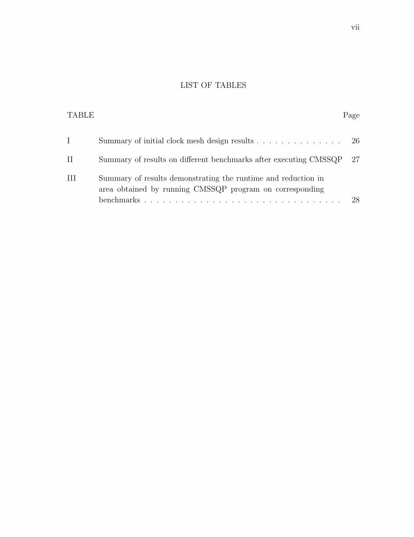
LIST OF TABLES
TABLE Page
I Summary of initial clock mesh design results . . . . . . . . . . . . . . 26
II Summary of results on different benchmarks after executing CMSSQP 27
III Summary of results demonstrating the runtime and reduction in
area obtained by running CMSSQP program on corresponding
benchmarks . . . . . . . . . . . . . . . . . . . . . . . . . . . . . . . . 28

viii
LIST OF FIGURES
FIGURE Page
1 A clock network with several levels of buffering and interconnect
wire segments. . . . . . . . . . . . . . . . . . . . . . . . . . . . . . . 1
2 Clock skew arising due to delay mismatch between the clock source
and target flip-flops. The skew till CLK1 is t1, till CLK2 is t2
and till CLK3 is t3. . . . . . . . . . . . . . . . . . . . . . . . . . . . 2
3 A clock mesh network comprising of a clock driver, a H-tree driv-
ing the mesh buffers, a clock mesh and the sink capacitances. . . . . 4
4 CMSSQP framework, flowchart depicting the different steps of
CMSSQP algorithm. . . . . . . . . . . . . . . . . . . . . . . . . . . 13
5 π model of a clock mesh. . . . . . . . . . . . . . . . . . . . . . . . . 14
6 Analysis flow of the adjoint sensitivity analysis framework. . . . . . 20
7 Original and adjoint circuits in the adjoint sensitivity analysis for
clock mesh. . . . . . . . . . . . . . . . . . . . . . . . . . . . . . . . 21
8 Detailed structure of the two-stage waveform independent gate
model. . . . . . . . . . . . . . . . . . . . . . . . . . . . . . . . . . . 22
9 Linearized gate model and its corresponding form in the adjoint
circuit. . . . . . . . . . . . . . . . . . . . . . . . . . . . . . . . . . . 23
10 Sink distribution in r1 benchmark. A point on the graph gives
the (x, y) location of a sink capacitance. . . . . . . . . . . . . . . . 25
11 Area-skew tradeoff by varying δ. . . . . . . . . . . . . . . . . . . . . 29
12 Case (a): (σ2 < δ), σ2, total clock mesh area in each iteration. . . . 29
13 Case (b): (σ2 > δ), σ2, total clock mesh area in each iteration. . . . 30

ix
FIGURE Page
14 Runtime of CMSSQP, runtime increases quadratically with mesh
size. . . . . . . . . . . . . . . . . . . . . . . . . . . . . . . . . . . . . 31

1
CHAPTER I
INTRODUCTION
The clock signal is one of the critical interconnect signals on a chip. A Clock Distribu-
tion Network (CDN) delivers the clock signal from the source to the target flip-flops.
There exist several topologies/architectures for the clock distribution networks [1].
A clock distribution network is shown in Fig. 1. which consists of multiple stages of
clock buffering and an interconnect network.
Fig. 1. A clock network with several levels of buffering and interconnect wire segments.
To distinguish the quality between the clock networks, the clock designers weigh
them based on the metrics like skew, slew and the power of a CDN. Designing a
clock network is always a compromise between accomplishable skew, slew, power and
The journal model is IEEE Transactions on Automatic Control.

2
routing resources. In this research work, we focus on formulating the problem with
the clock skew as a constraint.
The clock skew arises from a difference in latency from the clock source to the
target flip-flops on the chip. Various factors such as Process variations, Voltage,
Temperature (PVT) and cross coupling noise affect the clock skew [2–4]. If the clock
skew is not properly controlled, timing violations and system failures are possible.
Ideally, we wish to have “zero” skew which allows the accurate synchronization of
functionalities across the chip with an improvement in performance. Fig. 2. shows a
simple case where there is a delay difference between the clocks of the source and the
target flip-flops.
Fig. 2. Clock skew arising due to delay mismatch between the clock source and target
flip-flops. The skew till CLK1 is t1, till CLK2 is t2 and till CLK3 is t3.
The power is also a serious bottleneck for chips operating at a higher frequencies.
There is always a compromise between the achievable performance measured in terms
of frequency of the clock and the power dissipation inside the chip. Thus, the power
dissipated inside the chip is also emerging as an important consideration during the
design of a clock network. The clock distribution network dissipates up to 40% of
the chip power [5]. This includes only the dynamic power dissipated in the clock

3
network due to the charging and discharging of the clock node capacitances1. The
total capacitance to be driven by the clock buffers includes the capacitance of the
interconnect and the sink capacitance associated with the flip-flops.
The CDNs could be broadly categorized into trees and non-tree networks. In
many of the Application Specific Integrated Circuit (ASIC) designs, the clock is dis-
tributed across the chip using a clock tree. A clock tree network is a routing tree
where the clock driver is the root node and the clock sinks are the leaf nodes. The
clock tree synthesis is pretty much automated and it dissipates lesser power compared
to other CDNs. However, a clock tree has low tolerance to process variations.
When it comes to high-performance microprocessors there are stringent con-
straints on the maximum allowed clock skew. In such cases, the clock mesh offers
uniform, low skew clock distribution and offers better tolerance to On-Chip Variations
(OCV) than a conventional clock tree. A clock mesh network is a grid of interconnects
driven by buffers at various points and the clock sinks are connected to the nearest
wire segment of the mesh. To cope with the process variations, an attractive option
is to design a clock mesh which is robust and has higher tolerance towards process
variations [4]. The clock mesh uses the redundancy created by loops to even out the
delays across sink nodes distributed on the chip [4].
Many hybrid clock mesh topologies were analyzed in the past [1]. Among them
we use the topology with a uniform clock mesh that is driven by a global buffered
tree (as seen in Fig. 3.). The local interconnect referred as stubs, connects the clock
ports of flip-flops to the nearest point on the mesh. The clock mesh on the flipside
consumes a large area (metal resources) and dissipates higher power [6] compared
1The flip-flops are quantified using the gate capacitance of the clock port. Theflip-flops are often called as the sinks. The capacitance associated with the clock portin a flip-flop is called sink capacitance.

4
to the other CDNs. So, the clock mesh designs aim for a lower skew coupled with
targeting for lesser power.
Mesh Buffers
Clock Mesh
Sink Capacitances
Clock Driver
𝒆𝒍𝒆𝒎𝒆𝒏𝒕 𝒊 𝒘𝒊𝒅𝒕𝒉 = 𝒙𝒊
𝒂𝒓𝒆𝒂 = 𝒍𝒊 ∗ 𝒙𝒊
𝒔𝒊𝒏𝒌 𝒋
𝒅𝒆𝒍𝒂𝒚 = 𝒅𝒋
𝒕𝟏 𝒕𝟐 𝒕𝒊𝒎𝒆
A
B
A
B
Fig. 3. A clock mesh network comprising of a clock driver, a H-tree driving the mesh
buffers, a clock mesh and the sink capacitances.

5
A. Previous Works
Many of the research works like [2,3,7] centered on coping with the process variation
effects on the clock skew. This was anticipated as the process variations impact the
interconnects to a large extent and the clock signal is one of the most important
on-chip interconnect signal.
The research on CDNs could be categorized into problems focused on solving
clock tree and non-clock tree networks. The clock tree structures are well understood
and the algorithms were targeted to size the interconnect network and buffers driving
the clock tree in a divide-and-conquer fashion. However, this kind of approach is
difficult to straightaway apply to a clock mesh.
In the next section, we summarize the research done on clock networks, the
related optimization techniques and the approaches used to solve the problems for-
mulated.
1. Clock Tree Networks
The research work described in [8] uses a moment-based sensitivity analysis to reduce
the clock skew in a clock tree network. This is better than Elmore delay2computation
as it matches several moments in the delay calculations instead of the Elmore delay.
To improve the run-time of sensitivity-based methods they we also present heuristics.
This technique is restricted to a clock tree. It is difficult to extend the technique to
a clock mesh.
The objective of minimizing the skew under a power budget was proposed in [6].
They utilized Sequential Quadratic Programming (SQP) for solving the problem.
2Elmore delay is a simple first order approximation to the delay through an RCnetwork.

6
However, the SQP they used is not rigorous but is based on breaking down the prob-
lem into quadratic programming sub-problems using heuristics. They used a simple
extraction model for interconnect wire resistance and capacitance in a clock tree.
Even though their objective function was quadratic, the delay versus size function is
a linear approximation. Hence, its delay computation is inaccurate.
The clock tree sizing problem subject to skew constraints has been formulated in
[9]. The sensitivities of delays with respect to buffer and wire sizes were computed and
the power dissipated in the clock tree was minimized. Sequential Linear Programming
(SLP) was used as the optimization technique. Their methodology was to modify the
non-linear programming problem into a sequence of linear problems. The simulations
were performed using SPICE3model for clock buffers. They used a divide-and-
conquer approach to compute the sensitivities so that the SPICE run-time can be
reduced. The divide-and-conquer approach applies only to clock trees.
The clock tree’s relatively separable topology allows them to use sophisticated
algorithms and delay computations in a divide-and-conquer manner. However, it is
unclear how to extend them to a clock mesh.
2. Non-clock Tree Networks
The redundancy existing in a non-clock tree network offers resistance to PVT varia-
tions. However, the redundancy is often compromised to minimize the power. Non-
clock tree networks can be categorized into crosslinks and clock mesh.
3Simulation Program with Integrated Circuit Emphasis (SPICE) is a general-purpose circuit simulation program

7
a. Crosslinks
An algorithm based on inserting crosslinks in a clock tree network was proposed
in [10]. The link insertion scheme converts a clock tree into a non-clock tree network
to meet the skew constraint trading off wire length to achieve it.
The work in [11] investigates the buffer and wire sizing problem in a link based
non-tree clock network. The algorithms for crosslinks are mostly based on using
heuristics and are difficult to extend them to a clock mesh.
b. Clock Mesh
The timing uncertainty in clock-mesh based architectures has been analyzed in the
presence of parameter variations in [4]. They modeled the sources of uncertainties
assuming a distribution for parameter variations and obtained the delay distribution
curve at each flip-flop. It states that the clock mesh is efficient in reducing the timing
uncertainties. A Sliding Window Scheme (SWS) was proposed here to compute the
clock latencies in mesh-based architectures.
The problem of removing the non-critical wire segments in a clock mesh to min-
imize the power dissipated was formulated using network survivability theory [12].
Combinatorial algorithms were proposed to solve this problem.
The recent paper on Meshworks [13] proposed work on obtaining good quality
initial solution for a clock mesh. The problem of trading off skew and power has
also been addressed. The methodology deals with automated planning, synthesis and
optimization for a clock mesh. The problem uses Elmore model for the clock mesh
and the algorithm is a greedy heuristic.
In [14], network algorithms were proposed to solve the linear programs derived for
the sizing of interconnect elements of the clock mesh topology. The sizing algorithm

8
and the delay calculations were based on Elmore model of the interconnects. Due to
relative inaccuracy of Elmore model, this research is applicable only at early stages
of the design.
The design of a clock mesh is challenging as we need to use sophisticated delay
model for accurately measuring the delay values. The components in a clock mesh are
highly coupled with each other which makes it difficult to separate the original prob-
lem into smaller problems and solve. Some difficulties arise while trying to analyze
the clock mesh. They are: a large number of metal loops exist in a mesh structure
complicating the analysis [4], a large amount of memory and run-time is required for
the simulations, the clock mesh is difficult to model accurately [7] and the process
variations add difficulty in formulating the delay from clock root to flip-flop nodes.
The following section discusses about how this research work presented in the
thesis is dissimilar from the existing and previous works on clock networks.
B. Motivation and Our Contributions
As discussed previously, one of the significant challenges in clock mesh optimization
is the complexity of the network. The difficulty motivated the use of simple Elmore
models or partial SPICE solutions in earlier works and lead to various observed lim-
itations.
Various factors distinguish our work with many of the previous or existing works
on a clock mesh network. In this work, we first adopt a current-source based gate
modeling approach to speedup the accurate analysis of large mesh networks with near
SPICE accuracy. Further, we develop efficient adjoint sensitivity analysis capability
to provide desirable design sensitivity information, which allows a much more rigorous
application of SQP formulation, leading to improved solution quality and generality.

9
A rigorous Sequential Quadratic Programming (SQP) approach is used contrary
to many of the previous works which simply solve a nonlinear programming problem
through a sequence of quadratic approximations. We use the Karush-Kuhn-Tucker
(KKT) conditions to improve the computational efficiency. A quadratic delay formula
used in our problem improves the accuracy compared to a linear delay approximation
used in [6]. So, we use the quasi-newton approximation formula for obtaining the
second-order derivatives of variables considered in the problem.
To the best of our knowledge, our work is the first clock mesh sizing method
that does systematic solution search and is based on accurate delay model. Several
benchmarks from ISPD [15] and ISCAS [16] are evaluated using the algorithm. The
average improvement obtained in clock mesh area over the benchmarks is around
33%.
In the further sections we describe the efficacy of using a rigorous Sequential
Quadratic Programming (SQP) approach to solve the problem of minimizing the
power dissipation in a clock mesh satisfying the skew constraints. The variables we
sought to vary are the widths of the wire segments of a clock mesh.

10
CHAPTER II
CLOCK NETWORK OPTIMIZATION
A. Problem Formulation
Given a clock distribution network consisting of a clock mesh driven by a clock tree,
our objective is to minimize the power dissipation of the clock network while meeting
skew constraints by means of sizing the interconnects in the clock mesh. Independent
variables in this continuous optimization problem include the sizes of all the inter-
connects in the mesh. Power dissipation is approximately measured by the total wire
area. The skew is presented in a delay variance form. To restrict the skew among all
sinks of the network, the maximum value of delay variance is set by the problem.
Let I be the set of interconnects in the mesh. Denote by xi, i ∈ I the width/size
of element i in the interconnect set. The area of the ith element is represented by wi.
Apparently, the area occupied by a wire segment is linear to the its size. Let S be
the set of all the sinks of the network. Denote by dj, j ∈ S the propagation delay of
the signal from the root of the clock tree to sink j. Now, we formulate our problem
as follows:
Minimize: w =∑i∈I
wi = xTD, (2.1)
s. t. σ2 =∑j∈S
(dj − µ)2 ≤ δ, (2.2)
Lx ≤ x ≤ Ux,
where D is the coefficient vector reflecting the linear size-area relation, µ =∑
j∈S dj
|S| is
the average value of the sink delays, and δ is the given maximum variance. Lx and

11
Ux represent the lower bound, upper bound vectors of the wire widths respectively.
The skew constraint in the variance form has many advantages compared to
maximum skew formula. The quadratic form is a differentiable function whereas
maximum skew (∀(i, j ∈ S) Max|di − dj|) form is non-differentiable.
As an analogy, the quadratic cost can be thought of as connecting each pair of
sinks with a spring in the time domain and then trying to minimize the total energy
in the system of springs [6].
B. Algorithm Overview
The flow-chart shown in Fig. 4. summarizes the important steps of the Clock Mesh
Sizing using Sequential Quadratic Programming (CMSSQP) algorithm. The SPICE
netlist is generated with an initial topology of clock mesh for the specified benchmark.
The sensitivity analysis program generates the sensitivities of each wire segment in the
clock mesh with respect to its resistance and capacitance. Details of the sensitivity
calculations are provided in Chapter III. The sensitivities with respect to wire widths
are calculated with the help of chain rule in Eqn. 2.3.
∂σ2
∂X= (
∂σ2
∂R.∂R
∂X) + (
∂σ2
∂C.∂C
∂X) (2.3)
A transient simulation of the clock mesh gives the delay values with respect to
the input waveform at all sink nodes. We compute the delays from the transient
simulation waveform contrary to many of the previous works focused on calculating
the Elmore delays. We use compact delay models for the buffers driving the clock
mesh [17]. The quasi-newton approximation of the Hessian matrix is computed and
then the quadratic programming sub-problem is formulated and solved.
After completion of one iteration of the Clock Mesh Sizing using Sequential

12
Quadratic Programming (CMSSQP), we get the size change vector for all wire seg-
ments of the clock mesh. The wire segment widths vector is updated and the steps
described above are repeated in the same fashion until a convergence criterion is
satisfied.
The convergence criterion can be taken as a constant number of iterations or
until there is no significant reduction in clock mesh area in successive iterations.
We use strict sequential quadratic programming approach to solve the clock
mesh optimization problem. SQP is driven by gradient and Hessian of objective
and constraint functions. This information is needed to formulate the quadratic
programming sub-problems. Therefore, the sensitivity analysis is essential to provide
accurate gradient computation (information in Chapter III.). The sensitivity analysis
we used gives us the values of the sensitivities of skew variance constraint function
with respect to wire segment’s resistance and capacitance i.e. ∂σ2
∂Rand ∂σ2
∂C. These
values are used to compute the sensitivities of skew variance constraint function with
respect to wire segment’s width i.e. ∂σ2
∂Xusing a simple chain rule as given in Eqn. 2.3.
These values are used to solve the quadratic programming sub-problems. Fig. 5.
shows the π-model of a clock mesh. The resistance, capacitance values are calculated
for each wire segment of the clock mesh using the formulae displayed in the fig-
ure. The Hessian value is obtained in each iteration of CMSSQP using quasi-newton
method. The power dissipation is indirectly measured by the total interconnect area.
Reducing the clock mesh area reduces the interconnect load capacitance seen by the
buffers driving the clock mesh. Thus, reducing the clock mesh area reduces the total
dynamic power dissipation.

13
Transient Simulation
(Compute the delays, slew to every sink node)
Optimization
Formulate and Solve the Quadratic Programming
sub-problem
Update the widths of the clock mesh
Initialization of the design
(No. of buffers, benchmark and clock mesh)
Generate spice netlist
Sensitivity Analysis
(Sensitivities of the 𝜎2 with respect to wire widths)
Convergence
criterion met?
Quasi-Newton approximation of Hessian
NO YES
STOP
Fig. 4. CMSSQP framework, flowchart depicting the different steps of CMSSQP algo-
rithm.

14
W
H L
𝑹 =𝝆𝑳
𝑯𝑾
𝑪 =𝝐𝑳𝑾
𝑫
Fig. 5. π model of a clock mesh.
The following sections describe the SQP, sensitivity analysis and the results we
obtained.
C. Sequential Quadratic Programming (SQP) for Clock Network Sizing
1. Sequential Quadratic Programming
The delay (d) of signal to sinks is in complex relation to element sizes (x), which
make the constraint of clock network optimization problem very difficult to handle
in optimization. Our approach is to capture the sensitivity of skew variation with
respect to the size of all the elements in the network and improve the skew and
power consumption in a local region one step at a time. Intuitively, repeating this
improvement in multiple iterations makes the element size vector move towards the
best solution for the whole problem. This kind of strategy is backed up by a well-
founded optimization method called Sequential Quadratic Programming (SQP) [18].
Basically, SQP breaks the original problem into a sequence of sub-problems.

15
Each of these sub-problems is a Quadratic Programming problem (QP), which can
be solved efficiently. That is, the original highly complex problem is turned into
a sequence of quadratic programming problems. One set of critical values in this
transform are the gradient of the Lagrangian. Denote by L(x, λ) the Lagrangian of
the original problem in Eqn. 2.1. and Eqn. 2.2., i.e.,
L(x, λ) = xTD − λ(δ − σ2). (2.4)
Denote by ∇xL(x, λ) the gradient vector of the Lagrangian function, i.e.,
∇xL(x, λ) = D + λ∇xσ2. (2.5)
For a specific setup of all mesh wire widths in the clock network, the gradient
of sink delay variance, ∇xσ2, can be obtained by circuit simulation and advanced
sensitivity analysis, details of which is explained later in chapter III. In this section,
we use ∇xσ2 in our derivation as it is given by the sensitivity analysis.
To see how to solve the original problem given in Eqn. 2.1. and Eqn. 2.2., we
start with the Karush-Kuhn-Tucker (KKT) conditions of the problem, which are the
necessary conditions for any optimal point of the problem. The KKT conditions
imply that the gradient of the Lagrangian is zero and the constraints are satisfied at
the optimal point, i.e., for our problem,
D + λ∇xσ2 = 0, (2.6)
δ − σ2 ≥ 0. (2.7)
One common way to solve an equation as Eqn. 2.6. is Newton’s method. Basi-
cally, Newton’s method searches for the root of an equation f(x) = 0 in an iterative
matter. Starting from an initial point x0, the method finds the next approximation,

16
x1, by first order derivative. This operation continues in iterations until it converges
to the root. In the nth Newton iteration, the new approximation is calculated as
(Jn ∗ (xn+1 − xn)) = −f(xn), where Jn is the Jacobian matrix evaluated at xn,
(xn+1−xn) is a Newton step. In our case, the solution of Eqn. 2.6. is approached
by utilizing the same scheme.
Let the Newton step in iteration k of solving Eqn. 2.6. be px,k
pλ,k
=
xk+1
λk+1
− xk
λk
,where x and λ are all variables in the equation, px,k,pλ,k are the vectors representing
change in width of wires and Lagrangian multiplier.
The Jacobian of Eqn. 2.6. is given by:[∇2
xxL(x, λ) ∇xσ2
].
Denote by H = ∇2xxL(x, λ) the Hessian of the Lagrangian function. Then, the
Newton step calculation implies that px,k and pλ,k satisfy the following system:
[Hk ∇xσ
2k
] px,k
pλ,k
=
[−D − λk∇xσ
2k
]. (2.8)
Simple manipulation to Eqn. 2.8. gives us:
Hkpx,k +D + λk+1∇xσ2k = 0 (2.9)
Eqn. 2.9. can be solved by:
Minimize:
1
2pTxHpx +DTpx, (2.10)

17
s. t.
δ − σ2 ≥ 0,
which is the constraint given in Eqn. 2.7. Note that Eqn. 2.9. is actually a KKT
condition (zero gradient of Lagrangian function) of the optimization problem above.
Therefore, by transforming a Newton iteration, which solves the KKT conditions
given in Eqn. 2.6., into a Quadratic Programming (QP) problem, one iteration of
solving the original problem given in Eqn. 2.1. and Eqn. 2.2. is turned into a QP
sub-problem as following:
Minimize:1
2pTxHpx +DTpx, (2.11)
s. t. δ −(σ2 + (∇xσ
2)Tpx
)≥ 0, (2.12)
Lx ≤ x ≤ Ux,
where size step px consisting of size change for all elements in x is the solution of the
system. The multiplier step pλ is obtained from Newton’s step 2.8. given px.
After solving the QP sub-problem in Eqn. 2.11. and Eqn. 2.12. in an SQP
iteration, we get the step values px of the wire width variables. Then, the Lagrangian
multiplier’s step value pλ can be obtained from Eqn. 2.9. with known px. Thereafter,
the values of x and λ are updated accordingly.
There are various methods to solve the quadratic programming sub-problem in
2.11. and 2.12 efficiently. In order to formulate the QP sub-problem and give it
to a QP solver engine, we need to have both the gradient and the Hessian of the
Lagrangian function. As we have mentioned previously, through sensitivity analysis
we obtain the gradient. However, computing Hessian using techniques like sensitiv-
ity analysis is too expensive. The runtime is prohibitive in this way. Therefore, in
practice we approximate the Hessian given the gradient. Here, we use quasi-newton

18
method to approximate the Hessian H = ∇2xxL(x, λ).
To sum up the sequential quadratic programming (SQP) method above, we list
the major steps in each iteration of SQP in Algorithm 1. Line 3 in the outline of the
algorithm represents the operation of circuit simulation and sensitivity analysis. Line
4 is dedicated to formulate the QP sub-problem with calculated Hessian and gradient
and solve the sub-problem.
Algorithm 1 clockSQP
1: initialize (x0, λ0);
2: for all k ∈ {0, 1, 2, 3, ...} do
3: evaluate ∇xσ2 and H;
4: solve (11) and (12) to obtain pk;
5: xk+1 ← xk + px,k and λk+1 ← λk + pλ,k;
6: if converged, stop with solution (xk+1, λk+1);
7: end for
2. Quasi-Newton Approximation of Hessian
In this section, we describe the Hessian approximation method we utilize in this work.
Since the BFGS method [19] we use is a well-adopted quasi-newton algorithm, only
the major steps of the procedure are outlined here. Denote by H̃ the approximation
to the real Hessian. In iteration k + 1, the approximation H̃k+1 is calculated based
on H̃k from previous iteration.
To simplify the presentation, we define the changes on the wire width variables
and the gradient as follows.
sk = xk+1 − xk, (2.13)

19
yk = ∇xL(xk+1, λk+1)−∇xL(xk, λk+1). (2.14)
An effective modification of yk is defined as
rk = θkyk + (1− θk)H̃ksk, (2.15)
where
θk ={ 0.8sT
k H̃ksk
sTk H̃ksk−sT
k yk, if sTk yk < 0.2sTk H̃ksk
1, otherwise
The definition of θk above guarantees the approximation of the Hessian is always
positive definite when it is updated with the following formula.
H̃k+1 = H̃k −H̃ksks
Tk H̃k
sTk H̃ksk+rkr
Tk
sTk rk. (2.16)

20
CHAPTER III
SENSITIVITY ANALYSIS
The sensitivities in Eqn. 2.5. are obtained using adjoint sensitivity analysis. The ad-
joint sensitivity analysis [17] has been developed by Dr. Peng Li and Xiaoji Ye. The
idea of adjoint sensitivity analysis is to construct an adjoint circuit whose topology is
identical to the original circuit, by properly setting up the branch constitutive rela-
tions and input stimulus of the adjoint circuit, the desired sensitivity information of
the original circuit can be obtained by doing a convolution-like computation between
transient waveforms of the original and the adjoint circuit.
Original ckt
Transient simulation
Transientwaveforms
+
Linearized gate model
Adjoint ckt
Transient simulation
Post-processingof waveforms
Transientwaveforms
Sensitivity of the original ckt
Fig. 6. Analysis flow of the adjoint sensitivity analysis framework.
The analysis flow of the proposed adjoint sensitivity analysis framework is shown
in Fig. 6. First of all, we simulate the clock mesh to generate its transient waveforms.
Since we use compact gate model [17] instead of transistor level model for nonlin-
ear clock drivers, linearized compact gate model at every time point is saved for the

21
purpose of constructing the adjoint circuit later. Once the simulation of the original
circuit is finished, an adjoint circuit is constructed based on the original circuit, tran-
sient waveforms of the original circuit and linearized gate models. The adjoint circuit
is essentially a time-varying linear circuit. We then simulate the adjoint circuit to
obtain its transient waveforms. After the simulation of the adjoint circuit is finished,
we post-process the original transient waveforms and adjoint transient waveforms to
get the sensitivity information of the clock mesh. The original circuit/clock mesh
and its corresponding adjoint circuit are shown in Fig. 7. The detailed derivation and
formulas of the adjoint analysis can be found in [20].
Clock sink nodesClock drivers
V=0
V=0
V=0
V=0
Linearized clock drivers
Impulse I sources
Original circuit / clock mesh
Adjoint circuit
I=0Zero-value I sourcesClock signal
Fig. 7. Original and adjoint circuits in the adjoint sensitivity analysis for clock mesh.
Notice that clock mesh has nonlinear clock drivers which need special treatment.
In this work, we adopt the waveform independent gate model [17] to model nonlinear
clock drivers. The compact gate model provides up to two orders of magnitude
speedup over SPICE simulation while maintaining the same level of accuracy. The

22
detailed structure of the two-stage gate model is shown in Fig. 8. The first stage is
a second-order RC stage which models the internal gate delay. The output node of
the first stage is a fictitious node whose voltage response Vc is the controlling voltage
for the second stage. The second stage consists of a voltage-controlled current source
In(Vc, Vo) and a nonlinear capacitor Qnc(Vc, Vo), both of which are controlled by Vc
and the output voltage Vo of the gate.
R2
C2 C1
R1Vi+
-
Vc
In(Vc,Vo)
Qnc(Vc,Vo)
Vo
First stage Second stage
Fig. 8. Detailed structure of the two-stage waveform independent gate model.
The general principle of adjoint circuit analysis still holds for nonlinear circuits
since adjoint circuit analysis is derived from Tellegen’s theorem which only depends
on the Krichhoff’s Current and Voltage Laws. During the simulation of the original
circuit, at each timepoint, the nonlinear current source In and nonlinear capacitor
Qnc are linearized into linear elements,
In(Vc, Vo) =∂In∂Vc· Vc +
∂In∂Vo· Vo
= gc · Vc + go · Vo (3.1)
Qnc(Vc, Vo) =∂Qnc
∂Vc· Vc +
∂Qnc
∂Vo· Vo
= Cc · Vc + Co · Vo (3.2)
where gc·Vc represents a voltage-controlled current source, go is a regular conductance,
Cc represents a transcapacitance whose charge is controlled by Vc, Co is a regular

23
capacitor. In the adjoint circuit, go and Co remain the same; for controlled elements,
the controlling and controlled branches are swapped. The linearized gate model in
the original circuit and its corresponding form in the adjoint circuit are shown in
Fig. 9. Notice here the first stage of the gate model in the adjoint circuit is essentially
isolated from the entire circuit since it does not control the second stage or other part
of the circuit now. During the simulation of the original circuit, go, gc, Cc and Co
are varying, therefore, the adjoint circuit is a time-varying linear circuit. If different
gate model or transistor-level gate model is used to simulate the clock drivers in the
original circuit, we can still linearize each nonlinear element into linear elements and
apply the procedure for linear elements to handle them.
R2
C2 C1
R1Vi +
-
VcgcVc go Cc Co
Vo
R2
C2 C1
R1
Vi=0gcVo go Co
Vo
Cc
Linearized gate model in the original circuit
Its corresponding form in the adjoint circuit
Fig. 9. Linearized gate model and its corresponding form in the adjoint circuit.

24
CHAPTER IV
RESULTS AND CONCLUSIONS
A. Experimental Setup
The benchmarks are taken from International Symposium on Physical Design (ISPD [15])
and International Symposium on Circuits and Systems (ISCAS [16]). Sample formats
of these benchmarks are shown in appendix A. The Berkeley Predictive Technology
Model (BPTM [21]) 65nm technology transistor models are used for designing the
buffers driving the clock mesh. The clock mesh designed is a uniform grid of wires
spanning the entire area. A mesh of size (m×n) has m rows and n columns of wires.
The total area of the clock mesh is calculated with the formula given in Eqn. 4.1.
Total area of the clock mesh =∑i∈I
wili (4.1)
where wi is the width and li is the length of a wire segment within the clock mesh.
The mesh is driven by buffers placed uniformly on the clock mesh. The number of
buffers are adjusted such that the slew numbers are reasonable for the initial design.
The initial slew numbers are reported in Table I. The π model (refer to Fig. 5.) is
used for the interconnect wire segments of the clock mesh. The supply voltage is
1.2V. The skew among all the sinks in the clock mesh benchmark is calculated using
the formula: (∀(i, j ∈ S) Max|di − dj|) where di is the delay to the ith sink point.
All the different components of the Clock Mesh Sizing using Sequential
Quadratic Programming (CMSSQP) as can be seen in Fig. 4. are integrated on a
top-level using PERL [22] programming language. The sensitivity analysis has been
implemented in C++. The quadratic programming sub-problem in Eqn. 2.11. and
Eqn. 2.12. is solved using MOSEK [23] optimization engine.

25
The simulations are run on a Linux platform machine. It has two Intel Xeon
E5410 quad-core processors.
The benchmarks are profiled for the distribution of the sink capacitances. A
sample distribution of sinks for the benchmark r1 is shown in Fig. 10.
0
10000
20000
30000
40000
50000
60000
70000
80000
0 10000 20000 30000 40000 50000 60000 70000 80000
Sink Locations
Fig. 10. Sink distribution in r1 benchmark. A point on the graph gives the (x, y)
location of a sink capacitance.
This gives an estimate of the initial clock mesh size to be used. Some benchmarks
have sparse distribution of the capacitive loads and some have a dense distribution.
With reference to Table I., the number of sinks varies from a 91 to 3101 sinks con-
sidering all the benchmarks. The clock mesh designed varies in size from a (6× 6) to
(40 × 40) dense mesh over all the benchmarks. The subsequent section summarizes
the main results obtained using CMSSQP, solution quality, dependance of solution
with different design parameters and runtime of CMSSQP.

26
Table I. Summary of initial clock mesh design results
H-Spice ResultsBenchmark No. of Size of Initial
sinks mesh (before CMSSQP)Max Skew Max Slew Area
(ps) (ps) (µm2)ispd09f11 121 12X12 12.3 70.8 17160ispd09f12 117 12X12 16.9 55.2 20192ispd09f21 117 16X16 20.9 67.5 31590ispd09f22 91 16X16 16.2 51.5 17264
s1423 74 6X6 14.4 49.8 12439s5378 179 13X13 7.4 26.2 27189
s15850 597 24X24 14.9 37.4 62903r1 267 16X16 12.3 35.8 198589r2 598 30X30 22.3 59.2 499557r3 862 30X30 12.3 34.8 520200r4 1903 40X40 22.3 51.0 910821r5 3101 32X32 25.0 59.0 828123
Average 16.4 49.9 262168.9
B. Main Results
Tables I., II. and III. summarize the results obtained by executing CMSSQP pro-
gram on different benchmarks. Columns (1-3) in Tables I., II. and III. represent
the characteristics of the benchmarks. The benchmark name, number of sinks in that
particular benchmark and the clock mesh size designed are mentioned here. Columns
(4-6) in Tables I. and II. show the maximum skew, maximum slew and total clock
mesh area before and after executing the CMSSQP algorithm respectively. Columns
(4-5) in Table III. show the runtime and percentage reduction in clock mesh area by
running CMSSQP program on the corresponding benchmarks. The average reduc-
tion in clock mesh area achieved by running CMSSQP on all the benchmarks is about
33%. As seen, the CMSSQP achieves a significant reduction in clock mesh area.

27
Table II. Summary of results on different benchmarks after executing CMSSQP
H-Spice ResultsBenchmark No. of Size of Final
sinks mesh (after CMSSQP)Max Skew Max Slew Area
(ps) (ps) (µm2)ispd09f11 121 12X12 12.2 71 9914ispd09f12 117 12X12 17.4 52.1 11426ispd09f21 117 16X16 22.9 67.3 21473ispd09f22 91 16X16 19.9 51.1 14404
s1423 74 6X6 22 55.2 8614s5378 179 13X13 9.9 25.4 18888
s15850 597 24X24 17.4 42.3 47150r1 267 16X16 14.9 37.2 123931r2 598 30X30 29.7 66.7 363002r3 862 30X30 14.8 35 301505r4 1903 40X40 29.9 61.4 552229r5 3101 32X32 25.0 57.9 613754
Average 19.7 51.9 173857.5
As interpreted from the Eqn. 2.2., we have two cases:
1. Case when the skew constraint is relaxed. i.e. if (σ2 < δ), we have the freedom
to increase the σ2 close to δ, decreasing the total area of the clock mesh.
2. Case when the skew constraint is tight. i.e. if (σ2 > δ), CMSSQP drives the
solution towards satisfying the skew constraint by either increasing or decreasing
the total clock mesh area by non-uniform sizing of interconnect wire segment
elements.
Fig. 11. shows the trend between the total area of clock mesh and the allowed
maximum skew (considering all the sink pairs) for a benchmark ispd09f11. The skew
constraint is varied to obtain the values in the figure. As can be ascertained from the
figure, the amount of reduction in total area of clock mesh due to non-uniform sizing
of mesh elements is proportional to the skew constraint.

28
Table III. Summary of results demonstrating the runtime and reduction in area ob-
tained by running CMSSQP program on corresponding benchmarks
H-Spice ResultsBenchmark No. of Size of Runtime Area reduction
sinks mesh (s) (%)
ispd09f11 121 12X12 465 42.2ispd09f12 117 12X12 480 43.4ispd09f21 117 16X16 640 32.0ispd09f22 91 16X16 550 16.6
s1423 74 6X6 188 30.7s5378 179 13X13 322 30.5
s15850 597 24X24 1430 25.0r1 267 16X16 1197 37.6r2 598 30X30 2954 27.3r3 862 30X30 3115 42.0r4 1903 40X40 10540 39.7r5 3101 32X32 15440 25.9
Average 3110 33
Since, the Hessian matrix estimate starts with a unity matrix, it takes a few
iterations to get an accurate value. The minimum area satisfying the skew constraint
of (σ2 < δ) as in Eqn. 2.2. is obtained in a few iterations.
The design parameters such as lower bound of the wires (Lx in Eqn. 2.2.) and
upper bound of the wires (Ux in Eqn. 2.2.) can be changed to meet the desired skew
constraint. The vector of wire widths is limited to values ranging from 0.5×initial
width to 2×initial width. Fig. 12. represents the case (a), where the skew constraint
is relaxed. It shows the variation of the maximum skew among all the sink pairs and
the total area of the clock mesh collected for r1 benchmark in each iteration.
The maximum skew has only small increase of about 3ps. The increase of the
maximum slew is also very small. Whereas, the reduction in clock mesh area is
significant. Fig. 13. represents the case (b), where the skew constraint is tight.
As we can see CMSSQP drives the solution to satisfy the skew constraint at an
expense of increasing the total clock mesh area. Other benchmarks exhibit similar

29
12439.44
10871.16833
9977.58396
7515.510753
4000
5000
6000
7000
8000
9000
10000
11000
12000
13000
11.83 14.21 15.82 18.23
Total mesh area v.s. Max. skew
Fig. 11. Area-skew tradeoff by varying δ.
1400.0
1600.0
1800.0
2000.0
2200.0
2400.0
2600.0
1 2 3 4 5 6 7 8 9 10 11 12 13 14 15
iteration
100000.0
120000.0
140000.0
160000.0
180000.0
200000.0
220000.0
240000.0
1 2 3 4 5 6 7 8 9 10 11 12 13 14 15iteration
𝝈𝟐
Area
Fig. 12. Case (a): (σ2 < δ), σ2, total clock mesh area in each iteration.

30
0.0
100.0
200.0
300.0
400.0
500.0
600.0
700.0
800.0
900.0
1000.0
1 2 3 4 5 6 7 8 9 10 11 12 13 14 15 16 17 18
10000.0
11000.0
12000.0
13000.0
14000.0
15000.0
16000.0
17000.0
18000.0
1 2 3 4 5 6 7 8 9 10 11 12 13 14 15 16 17 18
𝝈𝟐
Area
Fig. 13. Case (b): (σ2 > δ), σ2, total clock mesh area in each iteration.
behavior for the cases (a) and (b). The summary of the improvement in area obtained
for the various benchmarks is specified in Table I.
C. Runtime
It was previously pointed out that the runtime for clock mesh simulations is large.
However, this difficulty is greatly subdued with CMSSQP. As discussed before, the
minimum possible value for clock mesh area is achieved in a few iterations of CMSSQP.
CMSSQP drives the solution monotonously towards satisfying the skew constraint.
This improves the overall runtime as it is a systematic search. With reference to
Fig. 4., the total time of CMSSQP can be approximated as the sum of time taken by
sensitivity analysis, transient simulation and optimization of quadratic programming
sub-problem. Fig. 14. shows the dependency of overall runtime of CMSSQP with
clock mesh density. We can easily observe that the number of wire segments increase

31
0
200
400
600
800
1000
1200
1400
10x10 20x20 30x30 40x40 50x50
Mesh Density
Run-time
(sec)
Fig. 14. Runtime of CMSSQP, runtime increases quadratically with mesh size.
quadratically with an increase in mesh density. Thus, the runtime for simulations
increase quadratically. Hence, the runtime of the algorithm increases quadratically
with the mesh density.
D. Conclusions and Future Work
The research work has been focused on sizing the interconnect elements within the
clock mesh. We believe that sizing the interconnect wire segments of the clock mesh
and the buffers driving the mesh simultaneously would yield more improvement in
the power of a clock mesh area satisfying the constraints. The work presented here
can be easily extended for sizing buffers and mesh elements simultaneously.
In this work, we have presented an algorithm for reduction of power satisfying
specified skew constraints in a clock mesh. It is fully automated and efficient in
terms of time and quality. The CMSSQP program is robust in dealing with any

32
complex clock mesh network. Also, the solution obtained is a systematic search
converging towards satisfying the skew constraint. Experimental results suggest that
the CMSSQP can achieve up to 33% reduction of total clock mesh area. This results
in a significant reduction in power consumed by the buffers.
The methodology developed is quite generic. It could be applied to any problems
which have the objective, constraint functions of the type specified in section 3. Thus,
it has been demonstrated that the CMSSQP is an efficient technique in minimizing
the the power while meeting the skew constraints in a clock mesh network.

33
REFERENCES
[1] C. Yeh, G. Wilke, H. Chen, S. Reddy, H. Nguyen, T. Miyoshi, W. Walker and
R. Murgai, “Clock distribution architectures: A comparative study,” in Proc. of
IEEE International Symposium on Quality Electronic Design, 2006, pp. 7–91.
[2] Y. Liu, S. R. Nassif, L. T. Pileggi and A. J. Strojwas, “Impact of interconnect vari-
ations on the clock skew of a gigahertz microprocessor,” in Proc. of ACM/IEEE
Design Automation Conference, 2000, pp. 168–171.
[3] J.P. Fishburn. “Clock skew optimization,” in IEEE Trans. Computers, pp. 945–
951, July 1990.
[4] S.M. Reddy, G.R. Wilke and R. Murgai, “Analyzing timing uncertainty in mesh-
based clock architectures,” in Proc. of IEEE/ACM International Conference on
Computer-Aided Design, 2006, pp. 1–6.
[5] D.E. Duarte, N. Vijaykrishnan and M. J. Irwin. “A clock power model to evaluate
impact of architectural and technology optimizations,” IEEE Trans. Very Large
Scale Integration, vol. 10, pp. 844–855, December 2002.
[6] M. R. Guthaus, D. Sylvester and R. B. Brown, “Clock buffer and wire sizing
using sequential programming,” in Proc. of ACM/IEEE Design Automation Con-
ference, 2006, pp. 1041–1046.
[7] M. Mori, H. Chen, B. Yao and C. Cheng, “A mulitple level network approach
for clock skew minimization with process variations,” in Proc. of Asia and South
Pacific Design Automation Conference, 2004, pp. 263–268.

34
[8] S. Pullela, N. Menezes and L. T. Pileggi, “Moment-sensitivity-based wire sizing
for skew reduction in on-chip clock nets,” IEEE Trans. Computer-Aided Design,
vol. 16, pp 210-215, February 1997.
[9] K. Wang, Y. Ran, H. Jiang and M. Marek-Sadowska, “General skew constrained
clock network sizing based on sequential linear programming,” IEEE Trans.
Computer-Aided Design,, vol. 24, pp. 773-782, May 2005.
[10] A. Rajaram, J. Hu and R. Mahapatra, “Reducing clock skew variability via
crosslinks,” IEEE Trans. Computer-Aided Design,, vol. 25, pp. 1176-1182, June
2006.
[11] R. Samanta, J. Hu and P. Li, “Discrete buffer and wire sizing for link-based
non-tree clock networks,” in Proc. of ACM International Symposium on Physical
Design, 2008, pp. 175–181.
[12] G. Venkataraman, Z. Feng, J. Hu and P. Li, “Combinatorial algorithms for fast
clock mesh optimization,” in Proc. of IEEE/ACM International Conference on
Computer-Aided Design, 2006, pp. 563–567.
[13] A. Rajaram and D. Z. Pan, “MeshWorks: An efficient framework for planning,
synthesis and optimization of clock mesh networks,” in Proc. of Asia and South
Pacific Design Automation Conference, 2008, pp. 250–257.
[14] M. P. Desai, R. Cvijetic and J. Jensen, “Sizing of clock distribution networks
for high performance CPU chips,” in Proc. of ACM/IEEE Design Automation
Conference, 1996, pp. 389–394.
[15] (2010, February 21) ISPD [Online]. Available:
http://www.sigda.org/ispd/contests/ispd09cts.html

35
[16] (2010, February 21) ISCAS [Online]. Available: http://www.pld.ttu.ee/ mak-
sim/benchmarks/iscas89/verilog/
[17] P. Li, Z. Feng and E. Acar, “Characterizing multistage nonlinear drivers and
variability for accurate timing and noise analysis,” IEEE Trans. Very Large Scale
Integration, vol. 15, pp. 1205–1214, November 2007.
[18] J. Stoer and K. Schittkowski, “Principles of sequential quadratic programming
methods for solving nonlinear programs,” in Computational Mathematical Pro-
gramming Ed. Series, vol. 15, Berlin, Germany: Springer-Verlag, 1984, pp. 165–
205.
[19] M. S. Bazaraa, D. S. Hanif and C. M. Shetty. Nonlinear Programming: Theory
and Algorithms, 3rd ed., New Jersey, Wiley, 2006.
[20] X. Ye and P. Li, “An application-specific adjoint sensitivity analysis framework
for clock mesh sensitivity computation,” in Proc. of IEEE International Sympo-
sium on Quality Electronic Design, 2009, pp. 634–640.
[21] (2010, February 21) BPTM [Online]. Available: http://www.eas.asu.edu/ ptm/
[22] (2010, February 21) PERL [Online]. Available: http://www.perl.org/
[23] (2010, February 21) MOSEK [Online]. Available: http://www.mosek.com/

36
APPENDIX A
# UCLA IBM clock benchmark 1.0
# Created : Wed May 17 10:47:57 PDT 2000
# User : [email protected]
# PlatForm : SunOS 5.7 sparc SUNW,Ultra-1
# Source : IBM benchmarks from R.S. Tsay
# Note : Coordinate unit can be micro-meter or anything
NumPins : 267
PerUnitResistance : 0.003000
PerUnitCapacitance : 2.000000e-17
Sink : 0
Coordinate : 29322 41420
Capacitive Load : 5.900000e-14
Sink : 1
Coordinate : 26208 51579
Capacitive Load : 3.500000e-14
Sink : 2 Coordinate : 35565 61661 Capacitive Load : 5.300000e-14 Sink : 3
Coordinate : 36852 64281
Capacitive Load : 3.400000e-14
Sink : 4
Coordinate : 33416 62525
Capacitive Load : 4.500000e-14
...........

37
ispd09f11 Benchmark:
0 0 11000000 11000000
source 0 0 0 0
num sink 121
1 621510 687103 35
2 431240 1449166 35
3 261732 2405588 35
4 701213 3334174 35
5 520350 4683492 35
6 549643 5698487 35
7 639090 6424544 35
8 394173 7738619 35
9 518009 8667593 35
10 545176 9270564 35
...........
num wirelib 2
0 0.0001 0.0002
1 0.0003 0.00016
num buflib 2
0 clkinv0.subckt 1 35 80 61.2
1 clkinv1.subckt 1 4.2 6.1 440
simulation vdd 1 1.2
limit slew 100
limit cap 118000
num blockage 0

38
VITA
Venkata Rajesh Mekala was born in Vetapalem, India. He completed his Bach-
elor of Engineering (Hons.) degree in electrical and electronics engineering from the
Birla Institute of Technology and Science, Pilani, India in June 2006. He subsequently
worked for one year as a design engineer before starting his graduate studies as a com-
puter engineering major at Texas A&M University in the Fall of 2007. His research
interests are in digital design and architecture, computer aided design for VLSI phys-
ical design. He can be reached at the following email address: [email protected].
His permanent address is SRT - 961, Flat # 202, Sanathnagar, Hyderabad, Andhra
Pradesh - 500018 - India.
The typist for this thesis was Venkata Rajesh Mekala.