Embed Size (px)
Citation preview

Extended Abstracts of tho 193 Intermtional Conf.r.occ on Solid State Dcvices and Materiab, M.kuhari, 1993, pp, 198-200 S-l- 1 - 1
Invited
Opto-Electronic Applications of Si,/Sir-,Gq Heterostructures
J.C. Sturm, )C )Gao*, Q. Mi+, and A- St. A.mourDepartment of Electrrical Engineering
Princeton OptoElectronic Materials Center (POEM)Princeton University, Princeton, NJ 08544 USA
L.C. Lenchyshya and M.L.W. ThewaltDepartment of Physics
Simon Fraser University, Burnaby, BC V5A1S6 Canada
+Present address: Intel Corp., Santa Clara, CA USA
Photoluminescence and electroluminescence can be obsewed in Si1-rGq/Siheterostructures grown by Rapid Thermal Chemical Vapor Deposition (RTCID)from 2K to 30OK and with peak wavelengths from 1.2 to 1.5 pm. This paperdescribes the emission mechanisms and a model for their temperature dependence.
Introduction
Despite the enormous progress in the field ofsilicon \ILSI in the past 30 years, practical lightemitting devices on silicon substrates haveremained an elusive goal. To overcome the prob-lem of indirect bandgap, it has been proposedthat certain short-period Si1-*Ge* superlatticeswould have a direct bandgap due to zone foldingeffects [1]. It is also known, however, that in arandom semiconductor alloy with an indirectbandgap, electrons and holes may recombinedirectly without phonons to emit light [2]. Thisis because the randomness of the alloy breaks theperfect translational symmetry of the crystal, andhence relaxes the requirement for momentum con-seryation. In photoluminescence spectra, thisIeads to a "no-phonon" (NIP) line in addition tothe usual phonon replicas in indirect bandgapsemiconductors. This effect has been observed inrelaxed bulk Si1-*Gq layers [3], single strainedSi1-*Ge* films [+], and in strained Si1-*Ge" quan-tum wells and superlattices [5]. This paperdescribes photo- and electroluminescence resultsbased on this alloy randomness effect in strainedSi1-*Ge*/Si quantum well structures.
Experiments and Modelling
The samples in this work were grown byRapid Thermal Chemical Vapor Deposition(RTCVD), which is described in more detail inRef. 6. The samples consist of single or multiplequantum wells of strained Si1_*Gq, followed by
Si capping layers. The Si layers were grown fromdichlorosilane in hydrogen at 700oC, and theSi1-*Ge* layers were grown at 625oC by addinggermane to the above gases. Typical photo-luminescence spectra at 2K are described in Ref.'s5 and 7. To summarize, the PL is due to excitonsbound by impurities at 2K and consists of theno-phonon line near the bandgap, a weaktransverse acoustic replica -15 meV below theNP line, and a series of transverse optical (TO)phonon replicas, the largest of which is the Si-Simode ^,58 meV below the NP line. At tempera-tures above LOK, the bound excitons become freeexcitons (or an electron holeplasma at high pumppowers [A]), but little change in the PL spectrais seen (except for broadening due to thermaland electron-hole plasma eflects). Typically theluminescence intensity changes by less than a fae-tor of two from 2I( to 77I< in struct,ures grown byRTC\ID. That the mobile free excitons do not allrecombine non-rad.iatively at midgap defectsconfirms the high quality of the CVD-grownlayers.
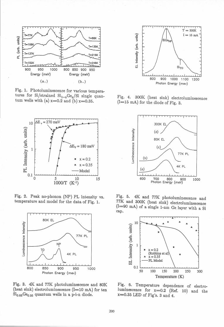
Above 77K, a strong decrease in the lumines-cence intensity is observed (Fig.'s 1 and Z forx:0.2, x:0.35, respectively). The temperatureabove which the luminescence decays stronglydepends on the germanium factor x in the well.For example, for x:O.Z, the NP luminescenceintensity has dropped by a factor of ten at a tem-perature of 160oC, while for x:0.35 this is notobserved until 27OoC. Furthermore, the activa-tion energies for the decay of the two signals are180 and 270 meV, respectively, close to theexpected bandgap offsets with respect to silicon.
198

This implies that a large bandgap offset from thecladding Si is necessary for high temperatureluminescence. Modelling shows that despite thelarge drop in PL intensity at high temperatures,nearly all carriers are still confined to theSi1-*Gq, however. To explain the decreased
luminescence, it becomes necessary to assume amuch lower effective lifetime in the Si claddinglayers than in the Si1-*Gq alloy, so that recombi-nation in the silicon controls the overall recombi-nation even though most carriers are in SiGe.This could be explained by defects at the sub-strate interface or recombination at the top sili-con surface. With such a model, the PL intensity(I) can be expected to scale as
T a y-+t (r + c#l.-anv/kr;-r (1)vv sice
where Wsi and Wsic. are the widths of the Si andSiGe active regions and where C is ^ constantrepresenting the ratio of effective SiGe to Si lifetimes. Using a single value of C, good agreementbetween the model and data is achieved (Fig. 2).
The luminescence can be pumped electricallyby placing the Si1-*Ge, quantum wells in the i-region of a p-i-n diode. At 4K, the NP and TOfeatures in this sample are clearly evident by PLand at the energy expected for the composition(FiS. 3), indicating recombination from barid-edgecarriers and not from defects. Similar features,althoug\ thermally broadened, are seen by PL at77K. In electroluminescence experiments at a,
heat sink temperature of 80K, the spectra arebroader still due to a higher junction tempera-ture, but the similarity to the 77K PL shows thatthe same band-edge mechanism is responsible forthe light. At a heat sink temperature of 300K,emission is still observable with a peak from theNP signal at 1.34 pm (Fig. 4). At room tempera-ture, the EL intensity increased linearly above a
current threshold density of 250 Af cmz, with anetimated lower limit to the internal quantumefficiency of O.O3% l9l.
To investigate longer wavelength emission, asing.le ^,1 nm Ge layer was grown at 625oC fol-lowed by a silicon cap. At room temperature,this structure electroluminescences over a broadband with a peak at 1.5 pm (Fig. 5). However, atlow temperature, neither the PL or EL is wellresolved, so that one cannot identify the lumines-cence mechanism. It is possible that the lightemission in this structure originates from defectsand not band edge carriers. Indeed, if no mixingoccurred, one could not expect the NP mechanismto be present in pure Ge layers.
The temperature dependence of the peakintensity of the x:0.35 LED of Fig's. B and { isshown in Fig. 6, along with the model results ofthe photoluminescenee of Fig. 2. One sees thatthe EL decay is much slower than the PL decayfor the same composition. Also shown is ELintensity vs. temperature for the x:0.2 LED's ofRobbins et, al. [fO]. While the x:0.2 EL decaysat a much lower temperature than that of thex:0.35 LED, it also decays much slower than thePL for similar composition. The reason for therelatively slow decay of the EL at high tempera-ture is presently under investigation.
Summary
The decay of the luminescence at h.igh tem-peratures in strained Si1_*Ge*/Si heterostructuresappeart to be controlled by recombination outsideof the Si1-*Gq layers, so that room temperaturephoto- and electro-luminescence requires asufficiently large bandgap offset and a low densityof non-radiative centers. Using d Sis.6sGq.ssquantum well grown by RTCVD, an LED withpeak emission of 1.3 pm and room temperaturequantum efficiency of 0.03% has been achieved.The support of NSF, OI\R, and the NJ Commis-sion on Science and Technology is gratefully ack-nowledged.
1. tI. Gnutzmann and K. Clausecker, Appl.Phys. 3, I (1e74).2, A.N. Pikhtin, Fiz. Tech. Poloprovodn. LL, 425(1977). [Sov. Phys. Semiconducr. LL, Z45 (1922)].3. J. Weber and M.I. Alonso, Phys. Rev. B40,5683 (1e8e).4. K. Terashima, M. Tajima and T. Tatsumi,Appl. Phys. Lett. 87, rg25 (1s90).5. J.C. Sturm, H. Manoharan, L.C. Lenchyshyn,M.L.W. Thewalt, N.L. Rowell, J.P. Noel and D.C.Houghton, Phys. Rev. Lett. 66, 1962 (fOOf ).6. J.C. Sturm, P.V. Schwartz, E.J. Prinz and H.Manoharan, J. Vac. Sci. Technol. Bg, 2011(1ee1).7, X. Xiao, C.W. Liu, J.C. Sturm, L.C. Len-chyshyn, M.L.W. Thewalt, R.B. Gregory and p.Fejes, Appl. Phys. Lett. 60, BLZT (1992).8. X. Xiao, C.W. Liu, J.C. Sturm, L.C. Len-chyshyn and M.L.W. Thewalt, Appl. Phys. Lett.60, L72O (1ee2).9. Q. Mi, X. Xiao, J.C. Sturm, L.C. Lenchyshynand M.L.W, Thewalt, Appl. Phys. Lett. OO, BLZT(1ee2).10. D.J. Robbins, P. Calcott, and W.Y. Leong,Appl. Phys. Lett. Es, Lss0 (1ss1).
r99
T-21 6K
T-248K
tt
c5ri0
aacq)
g
IJ
o.E5
€0
o.
900 950 1000 800 850 900 950tn..gy (mrv) Energy (mev)
(a. ) (b. )
Fig. 1. Photoluminescence for various tempera-tures for Si/strained Si1_*Ge*/Si single quan-tum wells with (a) x:0.2 and (b) x:0.8b.
270
AF.y = 180 meV
r x=0.2a x=0.35
- Model
5101000/T (K-t)
Fig. 2. Peak no-phonon (NP) PL intensity vs.temperature and model for the data of Fig. l.
8OK EL
800 850 900 950 loooPhoton Energy (mev)
Fig. 3. 4K and 77K photoluminescence and 80K(heat sink) electroluminescence (I:L0 mA) for tenSi6.6sGeq.ss euantum wells in a p-i-n diode.
800 900 1000 11oO 12oOPhoton Energy (mev)
FiS. 4. 300K (heat sink) electroluminescence(I:15 mA) for rhe diode of Fig. B.
10 5OOK EL
(d)
8OK EL
(")
(b)
I x=0.2(Robbins et
^ x=0.35
-PL Model
x'6cq)
gq)()cq)(Joo.gEf
(n
dl-{cg
blct)riodJn{
0.1
,^, 10Q
trudH
bl(t)trg
Flr4
,6cos(,ocoov,c).gEJ
l5 600 700 800 9oo 1o0oPhoton Energy (mev)
Fig. 5. 4K and TzK photoluminescence and77K and B00K (heat sink) electroluminrrcuor.(I:90 mA) of a single 1-nm Ge layer *iif, " Si
cap.
0.150 100 150 200 250
Temperature (K)
IiS. 6. Temperature dependence ofluminescence for x:0.2
- (Ref. 10)
x:0.35 LED of Fig's. B and 4.
300
electro-and the
200
![TSUBAKI KABELSCHLEPP Parts listkabelschlepp.ru/fileadmin/img/carrier/PDFs/spare... · Item Materialtext [remarks] KR 052 KR 065 KR 095 KR 125 KR 150 KR 180 KR 200 KR 225 1](https://img.dokumen.tips/doc/110x75/5faa70404ba8b17fd45cfabf/tsubaki-kabelschlepp-parts-item-materialtext-remarks-kr-052-kr-065-kr-095-kr-125.jpg)