Embed Size (px)
Citation preview

5
Circuit Sizing and Specification Translation
5.1 Introduction
Circuit sizing is defined as the process of finding out the parameter valuesof the dimensions of all the transistors (channel lengths and widths) and thevalues of the resistors and capacitors in a circuit, such that the desired perfor-mance objectives are optimized subject to a set of constraints that have to besatisfied [68]. The circuit sizing task is defined at the cell design level of ab-straction in the IC design flow. The similar task performed at the architecturedesign level of abstraction is referred to as the specification translation. Thespecification translation is defined as the task of mapping the specifications ofa block (e.g., a converter) under design to the individual specifications of thesub-blocks (e.g., a comparator) of the chosen block topology, such that thecomplete block meets its performance objectives optimally subject to a set ofconstraints that have to be satisfied [66, 139]. The task of circuit sizing andspecification translation are thus conceptually the same thing. The concept isrepresented in Fig. 5.1 [76]. This chapter presents a comprehensive overviewof the fundamental concepts behind the analog circuit sizing procedure.
5.2 Circuit Sizing as a Design Space ExplorationProblem
The circuit sizing problem is formally cast as a design space exploration prob-lem, which has been briefly introduced in Chapter 2 of this text. This isconsidered in detail below.
5.2.1 Problem Formulations
The design variables refer to those variables which are used by the circuitdesigners as decision variables. Design objectives include functional objectivesand performance objectives. The functional objectives need to be met by thedesign in order to be functionally right. The performance objectives, on the
217
Copyrighted Material - Taylor and Francis

218 Nano-Scale CMOS Analog Circuits: Models and CAD Techniques
FIGURE 5.1General design flow of a circuit sizing/specification translation task.
other hand, need to be minimized (or maximized). Let us consider the circuitof an output buffer, as shown in Fig.5.2 for illustration purpose [129]. Thedesign variable set α includes transistor dimensions and passive componentvalues. The possible functional objective set is [129] ρf which includes (1) DCGain (A0 > target), (2) input capacitance (Cin < target), (3) 3-dB frequency(f3dB > target), and (4) output swing (target < OS < target). The perfor-mance objective set ρf may be power consumption P . The design variable setαT = {α1, α2, ..., αn}T defines a multi-dimensional design space. Each of thedesign variables αi is bounded within an upper and a lower boundary. Thefunctional objective and the performance objective parameters are expressedas functions of the design variables, i.e., A0(α), Cin(α), f3dB(α), OS(α), P (α).Then the problem of circuit sizing is formulated as a constrained optimizationproblem; in particular, for the case of the buffer of Fig. 5.2 as,
Minimize P (α)
subject to A0(α) > target
Cin(α) < target (5.1)
f3dB(α) > target
target < OS(α) < target
and αiL < αi < αiU i = 1, 2, ..., n
Copyrighted Material - Taylor and Francis

Circuit Sizing and Specification Translation 219
IB
M6
M5 M7
M1 M2
M3 M4
M8
vin
v0
Cc
FIGURE 5.2A CMOS output buffer circuit.
5.2.2 Solution Techniques
There are two broad categories of techniques for solving problems of (5.1).These are (1) analytical techniques and (2) iterative techniques. Unfortu-nately, even for elementary analog circuits like that shown in Fig. 5.2 exactanalytical solution to the sizing problem is not possible. The primary reasonsare
1. The design equations (i.e., the functional relationships between thevarious functional and performance objectives on one hand and thevarious design variables on the other hand, which are nothing butthe performance and feasibility models) often cannot be expressedaccurately in pure analytic form, especially in the nano-scale regime.
2. Even if analytical representations of the design equations are pos-sible, these are often highly nonlinear, and consequently unsolvableanalytically. The situation becomes more complicated when the di-mensions of the design variable space and the design objective spacebecome large.
3. Even if the design equations are simple, analytical solution of (5.1)
Copyrighted Material - Taylor and Francis

220 Nano-Scale CMOS Analog Circuits: Models and CAD Techniques
No
New values of the
design variables
Design specifications
Specifications
met?
Solution
Yes
Optimization
algorithm
Feasibility
checking
Initialization of transistor dimensions/
specification parameters of the component
blocks
Cost function
computationPerformance evaluation
FIGURE 5.3Design space exploration process for circuit sizing/specification translationtask.
requires computation of the first and second derivatives of the designequations, which are in many cases very difficult to evaluate.
Therefore, analog circuits are most conveniently sized by using an iterative,dynamic process. This in turn can be done manually by the designers orthrough some automated design space exploration procedure.
5.2.3 Design Flow
The general flow of an automated design space exploration procedure for cir-cuit sizing using optimization algorithm is shown in Fig. 5.3. The procedurestarts with a set of design specifications. This consists of formal descriptionsof the various functional and performance objectives and the boundaries ofthe design variables. The design variables are initialized to some random val-ues within the boundaries. The various design equations (both performancemodels and feasibility models) are used to construct a cost function. The cost
Copyrighted Material - Taylor and Francis

Circuit Sizing and Specification Translation 221
function is evaluated with the initial values of the design variables and theevaluated results are checked against the design specifications. The subse-quent values of the design variables are generated through some optimizationalgorithms. The process is done iteratively until a set of design variables isobtained for which the desired design specifications are satisfied.
The two important modules of said procedure are (1) evaluation of costfunction through performance and feasibility models and (2) optimizationalgorithms. Chapter 4 of this book discusses in detail the construction ofthe performance and feasibility models. The implementation of the latter isdiscussed in the next section.
5.2.3.1 Evaluation of Cost Functions
The cost function is evaluated through some design equations. These designequations can be analytical equations or some learning network such as ANNand LS-SVM network, depending upon the complexity of the problem and thedegree of accuracy required.
5.3 Particle Swarm Optimization Algorithm (PSO)
Particle Swarm Optimization is a population-based search algorithm inspiredby the behavior of biological communities that exhibit both individual andsocial behavior; examples of these communities are flocks of birds, schoolsof fish, and swarms of bees. Kennedy and Eberhart introduced the conceptof function-optimization by means of a particle swarm [99]. A swarm is acollection of individuals or particles. Particles are conceptual entities, whichfly through the multi-dimensional design space. At any particular instant, eachparticle has a position and a velocity. The position vector of a particle withrespect to the origin of the design space represents a trial solution of the designproblem. Particles move randomly in the entire design space with velocitywhich is dynamically adjusted according to its own flying experience and theflying experience of the swarm. The movements of the particles are controlledby updating the position and velocity vectors of each individual particle in aneffort to find the optimum solution. The position of each particle is representedby a set of coordinates in the n-dimensional (n being the number of designvariables) design space of the exploration problem. The position vector of theith particle in an n-dimensional design space is given as
xi = [xi1, xi2, ..., xin]T
(5.2)
and the corresponding velocity vector is given by
vi = [vi1, vi2, ..., vin]T (5.3)
Copyrighted Material - Taylor and Francis

222 Nano-Scale CMOS Analog Circuits: Models and CAD Techniques
The position corresponds to the design variables that need to be optimized.At the beginning, a population of particles is initialized with random positionsand random velocities. The population of such particles is called swarm S. Ateach time step, all particles adjust their positions and velocities, i.e., directionsin which particles need to move in order to improve their current position, thustheir trajectories. The changes in the positions of the particles in the designspace are based on the social-psychological tendency of individuals to emulatethe success of other individuals. Thus each particle tends to be influenced bythe success of any other particle it is connected to.
5.3.1 Dynamics of a Particle in PSO
There are two main versions of the PSO algorithm, local and global. In thelocal version, each particle moves toward its best previous position and towardthe best particle within a restricted neighborhood. In the global version ofPSO, each particle moves toward its best previous position and toward thebest particle of the whole swarm. The global version is actually a special caseof the local version where the neighborhood size is the size of the swarm. Theposition and velocity of each particle is updated according to the followingtwo equations [100]
v(t+1)i = ω.v
(t)i + c1r1.
(
p(t)besti − x
(t)i
)
+ c2r2.(
g(t)besti − x
(t)i
)
(5.4)
x(t+1)i = x
(t)i + v
(t+1)i (5.5)
where pbesti represents personal best experience and gbesti represents the bestposition found so far in the neighborhood of the particle. When the neighbor-hood size is equal to the swarm size, gbesti is referred to as the globally bestparticle in the entire swarm.
The first term in the velocity updating formula represents the inertial ve-locity of the particle. ω is referred to as the “inertia factor”. Since it is thetendency to maintain the previous direction, it is called inertia. The secondterm represents the competition between the personally best position pbestithat each individual particle has experienced and its current position. c1 istermed as “self-confidence” [171]. The third term represents the particle’ssocial cognition or cooperation between the globally best position that oneparticle of the swarm has found and the current position of the particle. c2is termed as “swarm confidence” [171]. r1 and r2 stand for a uniformly dis-tributed random number in the interval [0, 1]. These are used to give diversityto the particles. The particle updates itself constantly sharing the informationboth from itself and the entire swarm in such a way that enables the particlesto move toward the optimum solution. The dynamics of the particle in a PSOalgorithm is illustrated in Fig. 5.4.
Copyrighted Material - Taylor and Francis

Circuit Sizing and Specification Translation 223
FIGURE 5.4Illustration of the dynamics of a particle.
5.3.2 Flow of the Algorithm
The algorithm starts with random initialization of the position and velocityof all the particles in a swarm. At the start of the simulation run, this initialposition of each particle is taken as the pbest of the respective particle and thefirst gbest is obtained from among these initial positions. A fitness function isused to search for the best position. As discussed in Chapter 2, this fitnessfunction is computed based upon the cost function of the problem. The fitnessfunction is computed based upon the current position of each particle. If thecurrent fitness value of a particle is better than the corresponding pbest, thenthe pbest location is updated with the current position value. If the currentbest fitness value is better than the gbest, then gbest position is replaced bythe current best position value of the entire swarm. The next position of eachparticle in the swarm is calculated based upon the dynamic equations (5.4)and (5.5). This iterative process continues until some termination criteria aresatisfied. This process is iterated, in general, for a certain number of timesteps, or until some acceptable solution has been found by the algorithms oruntil an upper limit of CPU usage has been reached. The flow chart of thePSO algorithm is shown in Fig. 5.5.
5.3.3 Selection of Parameters for PSO
The main parameters of a simple PSO algorithm are ω, c1, c2, Vmax and theswarm size S. The settings of these parameters determine how it optimizesthe design space exploration. However, it may be noted that the same param-eter settings do not guarantee success in different problems. Therefore, it isessential for the designers to understand the effects of the different settings,so that it is possible to pick a suitable setting from problem to problem [39].
Copyrighted Material - Taylor and Francis

224 Nano-Scale CMOS Analog Circuits: Models and CAD Techniques
Define solution space, swarm size,
maximum iteration, and desired goal
Randomly initialize particles with position
and velocity
Evaluate fitness for each particle
Current fitness
< pbest
Update
pbest=fitness
Current fitness
< gbest
Update
gbest =fitness
Update velocity and position
Limit velocity and position
Iter > max_iter
or
gbest < Desired goal
Terminate
Yes
No
Yes
No
No
Yes
FIGURE 5.5Flow chart of the PSO algorithm.
Copyrighted Material - Taylor and Francis

Circuit Sizing and Specification Translation 225
5.3.3.1 Inertia Weight ω
The momentum of the particle is controlled by the inertia weight. Therefore,if ω << 1, quick changes of direction of the movement of a particle is possible.If ω = 0, the concept of velocity is lost and the particle moves in each stepwithout the knowledge of the previous velocity. On the other hand, setting ωhigh (> 1) produces the same effect as setting c1 and c2 low. The particles canhardly change their directions which implies a larger area of exploration aswell as a reluctance against convergence toward optimum. Therefore, in shorthigh settings near 1 facilitate global search, and lower settings in the range[0.2, 0.5] facilitate rapid local search [39]. It has been reported that when Vmaxis not small (≥ 3), an inertia-weight of 0.8 is a good choice [170].
5.3.3.2 Maximum Velocity Vmax
The maximum change that one particle can undergo in its positional coor-dinates during an iteration is determined by maximum velocity Vmax. Thecommonly used approach is to set the entire range of the design space as themaximum velocity Vmax. The original idea of using this parameter is to avoidexplosion and divergence. However, with the use of ω in the velocity updateformula, the maximum velocity parameter becomes unnecessary to some ex-tent. Therefore, sometimes this parameter is not used. In spite of this fact,the maximum velocity limitation can still improve the search for optima inmany cases [39].
5.3.3.3 Swarm Size S
A common practice in selecting the swarm size is to limit the number ofparticles to the range 2060 [39]. It has been shown that though there is aslight improvement of the optimal value with increasing swarm size, a largerswarm increases the number of function evaluations to converge to an errorlimit.
5.3.3.4 Acceleration Coefficient c1 and c2
An usual choice for the acceleration coefficients c1 and c2 is to take c1 = c2 =1.494 [98]. An extensive study of the acceleration factor of PSO can be foundin [170]. Some researchers prefer to change these parameters in an adaptivemanner as follows [148]:
c1 = (c1f − c1i).iter
MAXITER+ c1i (5.6)
c2 = (c2f − c2i).iter
MAXITER+ c2i (5.7)
where c1i, c1f , c2i and c2f are constants, iter is the current iteration numberand MAXITER is the number of maximum allowable iteration. The basicidea behind the adaptive change of the acceleration coefficients is to boost
Copyrighted Material - Taylor and Francis

226 Nano-Scale CMOS Analog Circuits: Models and CAD Techniques
the global search over the entire search space in the initial part of the searchprocedure and to encourage the particles to converge to global optima at theend of the search.
5.4 Case Study 1: Design of a Two-Stage Miller OTA
The two-stage OTA circuit that has been considered in the present case studyis shown in Fig.5.6. The design variables are the transistor dimensions, biascurrent and the compensation capacitor Cc. The various design specificationsare (1) open loop gain Av, (2) gain-bandwidth GBW , (3) slew rate SR, (4)input common mode range ICMR, (5) output voltage swing and (6) powerdissipation Pdiss.
The various design equations related to the manual sizing of the two-stageCMOS OTA are summarized below based on [5]
1. From the desired phase margin, i.e., for a 60◦ phase margin, it is
FIGURE 5.6Schematic diagram of the Miller OTA.
Copyrighted Material - Taylor and Francis

Circuit Sizing and Specification Translation 227
chosen thatCc > 0.22CL (5.8)
where Cc is the compensation capacitor and CL is the load capaci-tor.
2. The tail current is selected from the slew rate requirement
I5 = SR.Cc (5.9)
3. Find gm1 from GBW and CC using the formula
gm1 = GBW.Cc (5.10)
Thereafter (W/L)1 is calculated as
(W
L
)
1
=
(W
L
)
2
=g2m1
2KpI1=
g2m1
KpI5(5.11)
where I1 = I5/2 and Kp = µ0Cox
4. From the positive ICMR requirement
VIC(max) = VDD − VSD5(sat)− VSG1 (5.12)
The current flowing through M1 is I5/2. Therefore, it can be writtenthat
VIC(max) = VDD −√
I5β1
− |VT1| − VSD5(sat) (5.13)
from which VSD5(sat) is calculated. Thereafter, (W/L)5 is calcu-lated as (
W
L
)
5
=2I5
KpV 2SD5(sat)
(5.14)
5. From the negative ICMR requirement, it follows that
VIC(min) = VS1 − VSG1 = VSD1 + VGS3 − VSG1 = VGS3 − |VT1|(5.15)
since the transistor M1 is to remain in saturation. From this VGS3is calculated, thereafter β3 and hence (W/L)3 is calculated usingthe following
VGS3 =
√
I5β3
+ VT3 (5.16)
Since VGS3 = VGS4 and M3 and M4 form a current mirror, we have(W
L
)
3
=
(W
L
)
4
(5.17)
Copyrighted Material - Taylor and Francis

228 Nano-Scale CMOS Analog Circuits: Models and CAD Techniques
6. For 60◦ phase margin, it is required that
gm7 ≥ 10× gm1 (5.18)
To achieve proper mirroring of the first stage current mirror load,it is required to ensure that VGS3 = VGS7. It is easy to show thatthis requires
(W
L
)
7
=
(W
L
)
3
.gm7
gm3(5.19)
where gm3 is found out from
gm3 =2I3
VGS3 − VT3=
I5VGS3 − VT3
(5.20)
Hence calculate
(W
L
)
7
7. The current through M7 is calculated as
I7 =g2m7
2Kn
(W
L
)
7
(5.21)
Since I7 = I8, and VSG8 = VSG5,
(W
L
)
8
is calculated as
(W
L
)
8
=
(W
L
)
5
.I7I5
(5.22)
8. The gain is calculated as
Av =2gm2gm7
I5 (λ2 + λ4) I7 (λ7 + λ8)(5.23)
The PSO is utilized for design specifications of gain Av ≥ 45dB, phasemargin > 450, GBW ≥ 2.5MHz 0.05V ≤ ICMR ≤ 0.6V , SR = 5V µs. Thetarget objective is to reduce the total MOS transistor area to smaller than3µm2.
Since the target gain is not high and the target area is very small, it ispreferred to take the channel length to be 0.1µm. The design variables are thechannel widths W and the compensation capacitor Cc. The inputs of PSOare set as VDD = 1V , VTn = 0.466V, |VTp| = 0.412V,Kn = 239µA/V 2, Kp =36µA/V 2. The swarm size is 35, ω = 0.99, C1 = C2 = 2. The constraintfunctions are based on the design equations outlined above. The equality con-straints are used to reduce the number of design variables. The target valuesof the specifications are selected so as to have sufficient guard band. The de-sign process is iterated over 1000 epochs with a total execution time of about
Copyrighted Material - Taylor and Francis

Circuit Sizing and Specification Translation 229
TABLE 5.1Aspect Ratios of Each Transistor of Case Study 1
Transistors W/LM1,M2 6.7M3,M4 27.3M5,M6 10.2M7 52.69M8 9.826CL 2.2pF
TABLE 5.2Comparison between PSO and Simulation Results of Case Study 1
Parameters PSO SPICEAv 48 dB 57.7 dBPM 600 500
GBW 3MHz 2.82MHzCMRR 60.78 dBICMR 0.1 to 6V 0.05 to 0.60V
Slew rate 5V/µs +ve 1.045V/µs and -ve 4.3V/µs
5s with an Intel Core 2 duo processor. The (W/L) values of the various MOStransistors are tabulated in Table 5.1.
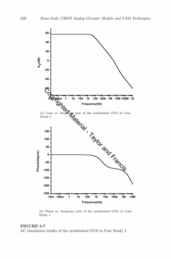
In order to validate the synthesized results, the design is implemented ina SPICE environment and simulated with 45nm CMOS technology with 1Vsupply. The simulation results are shown in Fig. 5.7(a), 5.7(b), 5.8(a), 5.8(b)and tabulated in Table 5.2
5.5 Case Study 2: Synthesis of on-Chip Spiral Inductors
This case study is in continuation of that described in Chapter 4 of thistext. The task of on-chip spiral-inductor synthesis refers to the process ofdetermining the layout geometric parameters from electrical specifications.The layout geometry parameters are (i) the outer diameter d, (ii) the num-ber of turns N , (iii) the metal width W and (iv) the spacing between themetal traces s. The spiral-inductor-synthesis procedure helps the designer tomake a trade-off analysis between the competing objectives, namely, Q, SRF ,and outer diameter d, for a given L. The synthesis flow is shown in Fig. 5.9[122]. The objective of the synthesis methodology is to find a set of layoutparameters which will give the desired inductance value within acceptableerror.
Copyrighted Material - Taylor and Francis
230 Nano-Scale CMOS Analog Circuits: Models and CAD Techniques
(a) Gain vs. frequency plot of the synthesized OTA in CaseStudy 1
(b) Phase vs. frequency plot of the synthesized OTA in CaseStudy 1
FIGURE 5.7AC simulation results of the synthesized OTA in Case Study 1.
Copyrighted Material - Taylor and Francis

Circuit Sizing and Specification Translation 231
(a) ICMR plot
(b) CMRR plot
FIGURE 5.8ICMR and CMRR results of the synthesized OTA in Case Study 1.
Copyrighted Material - Taylor and Francis

232 Nano-Scale CMOS Analog Circuits: Models and CAD Techniques
No
New values of the
design variables
through PSO
Design specifications
Specifications met?
Solution
Yes
Random initialization of the layout
parameters
Cost function computation
Computation of L, Q and
SRF through ANN-based
performance models
FIGURE 5.9Flow chart of the on-chip spiral inductor synthesis problem.
Copyrighted Material - Taylor and Francis

Circuit Sizing and Specification Translation 233
TABLE 5.3Synthesized Values of Inductor Layout Geometry Parameters
L(nH) d(µm) W (µm) N s(µm) Q SRF (GHz)3.9999 275 15.1 4.0 2.4 3.6122 10.2573.9968 284 13.1 3.0 1.4 3.639 11.5874.0041 252 11.7 3.9 2.5 3.1102 11.2074.0032 300 19.0 3.5 1.3 4.2953 9.1302
The design variable vector is α = [d,N,W, s]T. The cost function is for-
mulated as [122]
Minimize Ltarget − LANN
subject to Nmin ≤ N ≤ Nmax
dmin ≤ d ≤ dmax
Wmin ≤W ≤Wmax (5.24)
smin ≤ s ≤ smax
d ≥ 2N(W + s)− 2s
SRF ≥ SRFmin
The variables bounds are d = 100 − 300µm,W = 8 − 24µm,N = 2 − 6, s =1− 4µm and SRFmin = 6GHz.
The PSO algorithm generates a swarm of particles, each representing acombination of layout parameters in the given design space. For each combi-nation of the design variables, the performance parameters are computed froma pre-constructed ANN-based performance model. Cost function is computedusing these electrical parameter values. The design variables are then updatedaccording to the minimum cost following the PSO algorithm. This processcontinues until a desired cost function objective is achieved or the maximumnumber of iterations is executed. The error value is set to 0.0001nH and themaximum number of iterations is taken to be 1000.
Table 5.3 shows the layout geometries of the inductors as synthesized bythe proposed approach for a desired inductance value of 4nH at 1GHz oper-ating frequency [122]. A set of sample 4 layout geometries are reported here.This helps the designer to make a trade-off between Q, area (outer diameter),and SRF . It is to be noted that it may not be feasible to fabricate all theinductor geometries synthesized by this approach due to the design rules of aparticular process. For such cases the design values need to be rounded off tothe nearest grid point while doing the layout. To validate the accuracy of thesynthesis approach, the synthesized inductors are simulated with the IE3D EMsimulator. The synthesized inductors satisfy the desired design specifications.This is demonstrated in Table 5.4. The L, Q, and SRF of these inductorswere extracted from simulated S-parameters. The synthesized inductors showreasonable matching with the EM simulated results.
Copyrighted Material - Taylor and Francis
234 Nano-Scale CMOS Analog Circuits: Models and CAD Techniques
TABLE 5.4Verification of the Synthesized Inductor Geometry through EM Simulation
L(nH) Q SRF (GHz) d(µm) W (µm) N s(µm)PSO 4.0032 4.2953 9.1302 300 19.0 3.5 1.3EM 3.9389 4.150 9.5200 300 19.2 3.5 1.1
Error (%) 1.60 3.38 4.26
5.6 Case Study 3: Design of a Nano-Scale CMOS In-verter for Symmetric Switching Characteristics
This case study, based on the published literature [131] presents a techniquefor the modeling and design of a nano-scale CMOS inverter circuit using anANN and PSO algorithm such that the switching characteristics of the circuitis symmetric. This means that (i) the difference between the output rise time(τR) and fall time (τF ) and (ii) the difference between the output propagationdelay times, high-to-low (τPHL) and low-to-high (τPLH) should be minimum.The transistor channel widths Wn, Wp and the load capacitor CL are thedesign parameters. The value of the rise/fall time of the input signal will betaken from the user. The problem is therefore written as [131]
Minimize|τF − τR|
τF+
|τPHL − τPLH |τPHL
subject to (τF )min ≤ τF ≤ (τF )max
(τR)min ≤ τR ≤ (τR)max
(τPHL)min ≤ τPHL ≤ (τPHL)max
(τPLH)min ≤ τPLH ≤ (τPLH)max (5.25)
0.45× VSP ≤ VSP ≤ 0.55× VSP
and (Wn)min ≤Wn ≤ (Wn)max
(Wp)min ≤Wp ≤ (Wp)max
(CL)min ≤ CL ≤ (CL)max
The design flow of this circuit sizing problem is shown in Fig. 5.10. Thevarious performance parameters are evaluated through an ANN-based per-formance model. Thus the PSO algorithm would result in the exact valuesof the design parameters which minimize the cost function value and sat-isfy the specified constraints. The supply voltage VDD is taken to be 1.0V.The swarm size is taken to be 30. The acceleration parameters are taken asc1 = c2 = 1.49618 and the inertia weight factor is ω = 0.7298. This ensures
Copyrighted Material - Taylor and Francis

Circuit Sizing and Specification Translation 235
FIGURE 5.10Flow chart of the inverter design problem.
Copyrighted Material - Taylor and Francis

236 Nano-Scale CMOS Analog Circuits: Models and CAD Techniques
TABLE 5.5Delay Constraints and Design Parameter Bounds
τPHL τPLHSample CL(pF ) Wn(nm) Wp(nm) τF (ns) τR(ns) (ns) (ns)
1. 0.5-2.5 45-135 90-940 0.1-15 0.1-15 0.05-8.0 0.05-8.02. 0.5-2.5 45-110 90-620 0.1-15 0.1-15 0.05-8.0 0.05-8.03. 0.5-1.5 45-135 90-940 0.1-15 0.1-15 0.05-8.0 0.05-8.04. 1.0-3.0 60-160 160-945 0.1-15 0.1-15 0.05-8.0 0.05-8.05. 1.5-3.5 60-135 135-840 0.1-15 0.1-15 0.05-8.0 0.05-8.06. 0.3-2.0 45-90 90-540 0.1-8.0 0.1-8.0 0.05-6.0 0.05-6.07. 0.6-1.9 60-160 135-910 0.1-7.5 0.1-7.5 0.05-5.5 0.05-5.5
TABLE 5.6Synthesis Results: τin = 1ns
CL Wn Wp τPHL τPLHSample (pF ) (nm) (nm) τF (ns) τR(ns) (ns) (ns) Vsp(V )
1. 0.83 128.37 221.93 5.1546 5.1363 2.5277 2.4648 0.48902. 0.76 69.44 100.08 10.5131 10.5820 4.8127 4.8025 0.48613. 0.81 125.82 217.53 5.0244 5.1146 2.6854 2.6731 0.48794. 1.02 157.91 273.01 5.2138 5.2015 2.5812 2.5637 0.48515. 1.66 134.70 232.88 8.8279 8.8588 4.6977 4.6785 0.48006. 0.42 65.42 113.10 5.4471 5.4233 2.5805 2.5332 0.48877. 0.61 95.52 165.14 5.3867 5.3678 2.7219 2.7581 0.4876
good convergence of the PSO algorithm. The maximum number of iterationsthat has been considered is 1000.
A set of seven samples has been chosen. For each sample, the desiredrise time, fall time, low-to-high and high-to-low output propagation delaytimes are kept within a certain constraint, defined by an upper limit and alower limit. Similarly, the design parameters are also kept within a specifiedbound. These are tabulated in Table 5.5 [131]. The value of the input risetime/fall time τin is assumed to be 1ns. The synthesized values of the designparameters corresponding to which the cost function is minimized and theconstraints are satisfied for all the case studies, are shown in Table 5.6 [131].It also contains the corresponding values of the performance parameters. It isobserved from Table 5.5 and 5.6, that the synthesized parameters satisfy thedesign constraints.
In order to validate the results obtained through PSO optimization, thedesign samples are selected and implemented at the transistor level. The PSOsynthesized transistor widths and output load capacitor values have been con-sidered. The channel length is taken as 45nm with 1.0V supply. Transientsimulation is then performed using SPICE simulation. A comparison betweenthe PSO generated results and SPICE results is provided in Table. 5.7-5.8
Copyrighted Material - Taylor and Francis

Circuit Sizing and Specification Translation 237
TABLE 5.7Comparison between PSO Results and SPICE Results: τR and τF
Sample PSO Results SPICE ResultsτR(ns) τF (ns) Diff(ns) τR(ns) τF (ns) Diff(ns)
1. 5.1363 5.1546 0.0183 5.0674 5.2532 0.18582. 10.5820 10.5131 0.0689 10.6200 9.8351 0.78493. 5.1146 5.0244 0.09012 5.0535 5.3356 0.28214. 5.2015 5.2138 0.0123 5.0398 5.4025 0.36275. 8.8588 8.8279 0.0309 8.6485 8.5699 0.07866. 5.4233 5.4471 0.0238 5.2171 5.6551 0.4387. 5.3678 5.3867 0.0189 5.2649 5.6741 0.4092
TABLE 5.8Comparison between PSO Results and SPICE Results: τPHL and τPLHSample PSO Results SPICE Results
τPHL(ns) τPLH(ns) Diff(ns) τR(PHL) τF (LH) Diff(ns)1. 2.5227 2.4648 0.0579 2.6455 2.4367 0.20882. 4.8217 4.8025 0.0192 4.9417 4.9256 0.01613. 2.6854 2.6731 0.0123 2.8366 2.4292 0.40744. 2.5812 2.5637 0.0175 2.5157 2.4210 0.09475. 4.6977 4.6785 0.0192 4.7861 4.5264 0.25976. 2.5805 2.5332 0.0473 2.5771 2.4957 0.08147. 2.7219 2.7581 0.0362 2.8629 2.6367 0.2262
[131]. It is observed that the PSO generated designs yield very good resultseven when simulated at the SPICE level as far the symmetry of the switchingcharacteristics is considered.
5.7 The gm/ID Methodology for Low Power Design
By now it is clear to the readers that sizing of an analog circuit while meetingsimultaneously a large number of objectives like a prescribed gain-bandwidthproduct, minimal power consumption, minimal area, low-voltage design, dy-namic range, non-linear distortion, etc., is a very difficult task. This becomesmore complicated when the transistors are designed with nano-scale tech-nology. Optimization algorithms are attractive without any doubt, but theyrequire translating not always well-defined concepts into mathematical ex-pressions. The interactions amid semiconductor physics and analog circuitsare not always easy to implement [93].
This section presents a methodology for sizing of CMOS analog circuits so
Copyrighted Material - Taylor and Francis

238 Nano-Scale CMOS Analog Circuits: Models and CAD Techniques
as to meet specifications such as gain-bandwidth while optimizing attributeslike low power and small area. The sizing method takes advantage of the gm/IDratio of a MOS transistor and makes use of a set of look-up tables. Thesetables are derived from physical measurements carried out on real transistorsor advanced compact models such as BSIM4.
5.7.1 Study of the gm/ID and fT Parameters for AnalogDesign
An important challenge in analog design is to achieve a good balance betweenthe bandwidth and power efficiency of a circuit [133]. The two parameterswhich appear to be very much significant to the analog designers are (1)gm/ID and (2) fT = gm/2(πCgg). The former signifies the amount of currentto be used per transconductance and the later parameter signifies how muchtotal gate capacitance Cgg must be driven at the controlling node per desiredtransconductance. The values of these quantities are found to be dependenton the region of operations of a MOS transistor. This is demonstrated in Fig.5.11(a) and 5.11(b). It is observed that the gm/ID parameter has the maxi-mum value in the weak inversion region and the value decreases as the oper-ating point moves toward the strong inversion region. On the other hand, thefT parameters has minimum value in the weak inversion region and the valueincreases as the operating point moves toward the strong inversion region.In addition, it is observed that the gm/ID parameter is not very sensitive totechnology scaling. On the other hand, the values of fT increase significantlywith technology scaling.
It is interesting for the analog designers to study the variations of the prod-uct of gm/ID and fT with the region of operation. This is shown in Fig. 5.12.This helps the designers to determine the overdrive voltage, i.e., (VGS − VT )such that the bandwidth objective is met while operating at the correspond-ing maximum possible gm/ID (lowest power). It is observed that for a giventechnology node, the product quantity exhibits a “sweet spot” around a gateoverdrive of 100 mV, which is a commonly found bias condition in many oftoday’s moderate-to-high speed designs [133]. On the other hand, working withhigh gm/ID greatly helps in reducing power consumption for applications thatdo not demand an extremely high bandwidth. For such applications, the MOStransistors can be biased in the weak inversion region. However, operating inthe weak inversion region with high gm/ID comes at the cost of degradedlinearity performance of the transistor. This is illustrated in Fig. 5.13 , whichshows the linearity performance of various technologies versus gm/ID. Thelinearity is characterized through the parameter VIP3 which represents theextrapolated gate-voltage amplitudes, at which the third-order harmonics be-come equal to the fundamental tone in the drain current ID. Mathematically,this is expressed as [202]
VIP3 =
√
24gmgm3
(5.26)
Copyrighted Material - Taylor and Francis

Circuit Sizing and Specification Translation 239
(a) variation of gm/ID
(b) variation of fT
FIGURE 5.11Simulation results for the variations of gm/ID and fT with the region of op-eration and technology nodes.
Copyrighted Material - Taylor and Francis

240 Nano-Scale CMOS Analog Circuits: Models and CAD Techniques
FIGURE 5.12Simulation results showing the variations of the product of gm/ID and fTwith the region of operation and technology node.
FIGURE 5.13Simulation results showing the variations of the transconductance linearitywith the region of operation and technology node.
Copyrighted Material - Taylor and Francis

Circuit Sizing and Specification Translation 241
where gm3 =∂3ID∂V 3
GS
. The VIP3 peak, which is shown in Fig. 5.13, is because of
the second-order-interaction effect and can be explained as a cancellation ofthe third-order nonlinearity coefficient by device internal feedback around asecond-order nonlinearity. In practice, it is very hard to utilize this extremelylinear point. It is observed that the linearity is degraded as the gm/ID ratiois increased.
It is also important to study the variations of the intrinsic capacitances ofMOS transistors as functions of the gm/ID parameter. These are shown in Fig.5.14(a) and 5.14(b). It is observed that the values of the both the capacitorsare low, when gm/ID is high.
5.7.2 gm/ID Based Sizing Methodology
The gm/ID based circuit sizing procedure is based on the relation betweenthe ratio of the transconductance over DC current gm/ID and the normalizedcurrent IN = ID/(W/L)[173, 34]. The selection of the gm/ID as the keyparameter is due to three reasons. First, this parameter is strongly related tothe analog performances. Second, it gives an indication of the operating regionof a MOS transistor. Third, it provides a tool for calculating the transistordimensions. This parameter is considered to be a universal characteristic of thetransistors in the same process technology. The relation between the gm/IDparameter with the operating region of the transistor may be written as follows
gmID
=1
ID
∂ID∂VGS
=∂ (ln ID)
∂VGS=
∂
ln
IDS(W
L
)
∂VGS(5.27)
As it has been demonstrated in Fig. 5.11(a) the maximum value of the gm/IDratio lies in the weak inversion region and the value decreases as the operatingpoint moves toward strong inversion when ID or VGS are increased. It maybe noted that the gm/ID ratio is independent of the transistor sizes. Thenormalized current IN is also independent of the transistor sizes. Therefore,the relationship between the gm/ID and the normalized current is a uniquecharacteristic for all transistors of the same type (n-channel MOS or p-channelMOS) in a given batch. This relationship is shown in Fig. 5.15(a) and Fig.5.15(b). This universal characteristic of the gm/ID versus IN curve is used todetermine the aspect ratio of a transistor, which is then subsequently used todetermine the channel width, assuming a fixed value of the channel length.The corresponding simulation graph is shown in Fig. 5.16.
For a MOS transistor, the magnitude of the intrinsic voltage gain is givenby
Av = gmr0 =
(gmID
)
(IDr0) =
(gmID
)
VA (5.28)
Copyrighted Material - Taylor and Francis

242 Nano-Scale CMOS Analog Circuits: Models and CAD Techniques
(a) variation of CGS
(b) variation of CGD
FIGURE 5.14Simulation results for the variations of CGS and CGD with the gm/ID.
Copyrighted Material - Taylor and Francis

Circuit Sizing and Specification Translation 243
(a) gm/ID for n-channel and p-channel MOS transistor
(b) gm/ID graph for different aspect ratios
FIGURE 5.15Simulation results for the gm/ID variations.
Copyrighted Material - Taylor and Francis

244 Nano-Scale CMOS Analog Circuits: Models and CAD Techniques
Z
FIGURE 5.16Simulation results showing the variations of the gm/ID with the normalizedcurrent IN .
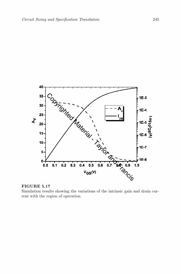
where VA is referred to as the early voltage of the transistor. Assuming VAto be constant for a particular channel length of a transistor, the intrinsicgain is determined by the gm/ID ratio. Therefore, the intrinsic gain of a MOStransistor is maximum in the weak inversion region and reduces as the oper-ating point moves toward the strong inversion region. This is shown in Fig.5.17. Therefore, an important guideline to get high gain for a MOS transis-tor, is to bias the transistor in the weak inversion region with as low VGSas possible. An interesting thing observed from the curve is that under weakinversion regions very small amounts of drain current flows, which implies asmall amount of power dissipation. Therefore, by biasing the MOS transistorin the weak inversion region, it is possible to obtain high gain with very smallpower dissipation.
The procedure for determining the aspect ratio through the gm/IDmethodology is explained by a simple example. Let the current flow throughthe transistor be ID = 100nA. The transistor is biased in the weak inversionregion with gm/ID = 21.8V −1 at VGS = 0.3V . From the normalized currentplot, it is observed that the corresponding IN = 41.64nA. Therefore, the as-pect ratio is found to be W/L = 2.4. Therefore, by assuming L = 100nm, thechannel width is found to beW = 0.24µm. The power dissipation correspond-ing to a supply voltage of 0.5V will be 50nW.
Copyrighted Material - Taylor and Francis
Circuit Sizing and Specification Translation 245
FIGURE 5.17Simulation results showing the variations of the intrinsic gain and drain cur-rent with the region of operation.
Copyrighted Material - Taylor and Francis

246 Nano-Scale CMOS Analog Circuits: Models and CAD Techniques
The primary advantage of the gm/ID methodology over other method-ologies is that this methodology uses a set of look-up tables as the maindesign tool, which is itself constructed from SPICE simulations. Therefore,the predicted results, as obtained after the circuit sizing process, appear tobe quite close to the actual SPICE results. The same can be achieved by us-ing ANN/LS-SVM based models. However, construction of look-up tables ismuch easier and less time consuming. Therefore, the gm/ID methodology isgaining importance day by day for nano-scale analog circuit design. In addi-tion, the gm/ID methodology gives the designers the flexibility to operate thetransistors in any region of operation. It may be noted that by using compactmodels, it is possible to compute the gm/ID graph analytically.
5.7.3 Case Study 4: Sizing of Low-Power Nano-Scale MillerOTA Using the gm/ID Methodology
The sizing methodology of a Miller OTA circuit, shown in Fig.5.6 , is basedon what is presented in [173, 34]and is outlined below.
1. From the power consumption requirement, the total current IT flow-ing through the circuit is calculated.
2. The compensation capacitor Cc is calculated from the 60◦ phasemargin requirement, Cc > 0.22CL.
3. The bias current is determined from the slew rate requirement. Ib =I5 = SR.Cc
4. The second-stage branch current is calculated as I8 = I7 = IT −2Ib
5. From the gain-bandwidth requirement, the transconductance of M1
transistor is calculated as GBW =gm1
2πCc
6. Fix
(gmID
)
1
to operate the M1 transistor in weak inversion.
7.
(gmID
)
1
=
(gmID
)
2
8. The transistors M3 and M4 are operated in the weak inversion re-gion since the current flowing through these transistors is small.
Select the
(gmID
)
3
and
(gmID
)
4
sufficiently high.
9. The transistors M5, M6 and M8 are similarly made to operate in
the weak inversion region and the
(gmID
)
ratios are determined
accordingly.
10. From the relation gm7 >> 10.gm1, find out gm7 and hence
(gmID
)
7
Copyrighted Material - Taylor and Francis

Circuit Sizing and Specification Translation 247
TABLE 5.9Aspect Ratios and gm/ID Ratio of Each Transistor of Case Study 4
Transistor W/L gm/IDM1 230 24.7M2 230 24.7M3 4 23.43M4 4 23.43M5 459 24.7M6 459 24.7M7 14 22.73M8 2526 24.7
TABLE 5.10Comparison between Analytical and Simulation Results for Case Study 4
Performances Analytical SimulationGain (db) 60 41.4
GBW (KHz) 50 56SR (V/µs) 0.025 0.02CMRR(db) 71.9ICMR(V) (0.065 to 0.9)
Total current (nA) 300 299
11. Once the
(gmID
)
of all transistors and the corresponding drain cur-
rents are known, the normalized current are determined from the
gm/ID vs IN graph and hence the
(W
L
)
ratios for each transis-
tor are determined from the corresponding normalized currents anddrain currents.
It may be noted that an important issue related to the operation of MOStransistors in a weak inversion region is that under this condition, the draincurrent mismatch due to threshold voltage mismatch is maximum. Therefore,often the transistors involved in the current mirror circuit are not operated inthe weak inversion region. Therefore, the gm/ID ratios of such transistors areto be selected accordingly.
With the present methodology it is attempted to design a two-stage MillerOTA with gain Av > 40dB, gain bandwidth product GBW ≥ 40KHz, phasemargin PM > 600, slew rate SR = 25V/ms and power dissipation ¡350nW.
The transistor length is considered to be 0.1µm. The length can be in-creased, if higher gain is required. The aspect ratios as well as the (gm/ID)ratio of each transistor are tabulated in Table. 5.9. The circuit is simulatedusing 45nm,1V CMOS technology using HSPICE simulation tool. Table 5.10
Copyrighted Material - Taylor and Francis

248 Nano-Scale CMOS Analog Circuits: Models and CAD Techniques
(a) Gain vs. frequency plot of the synthesized OTA
(b) Phase vs. frequency plot of the synthesized OTA
FIGURE 5.18AC simulation results of the synthesized OTA in Case Study 4.
Copyrighted Material - Taylor and Francis

Circuit Sizing and Specification Translation 249
(a) CMRR
(b) Slew rate
FIGURE 5.19CMRR and slew rate of the synthesized OTA in Case Study 4.
Copyrighted Material - Taylor and Francis
250 Nano-Scale CMOS Analog Circuits: Models and CAD Techniques
shows the comparison between the performances as calculated analyticallyand as obtained from SPICE simulation results. The AC simulation resultsillustrating the variations of the gain and phase with frequency for the syn-thesized OTA are shown in Fig. 5.18(a) and Fig. 5.18(b). The CMRR andthe slew rate is obtained from Fig. 5.19(a) and Fig. 5.19(b) respectively. Thedifference between the analytical and simulation results occurs primarily be-cause of the fact that the variations of the early voltage with drain bias arenot taken into consideration in this method. This is an important issue innano-scale design and needs to be taken care of judiciously.
5.8 High-Level Specification Translation
At the architectural level of abstraction of a hierarchical analog designmethodology, the overall architecture of the system is first decomposed intoseveral component blocks. The specifications of these component blocks arethen derived from the specifications of the complete system so that they canbe designed separately. This is referred to as the process of high-level specifi-cation translation [139]. For example, if the system to be considered is a Σ−∆ADC, then at the architecture level, the component blocks are the integrator,comparator, etc. The specifications of these component blocks need to be de-rived such that the system specifications are optimally satisfied. On the otherhand, at the same time, it has to be ensured that the specifications of thecomponent blocks can actually be realized in practice, finally when the var-ious component blocks are to be implemented using transistor-level circuits.Therefore, the task of high-level specification translation is a challenge to theanalog designers.
The task of construction of feasible design space as an intersection of an ap-plication bounded space (constructed by top-down procedure through intervalanalysis technique) and circuit realizable space (constructed by bottom proce-dure through actual circuit simulation) and subsequent identification throughLS-SVM classifier method has been discussed in [139]. This has been describedin detail in Chapter 4 of this text. The identified feasible design space needsto be explored through any design space exploration algorithm such as theparticle swarm optimization algorithm or genetic algorithm etc., in order tofind out the various values of the design parameters. Recently a geometricprogramming-based methodology has been used for high-level specificationtranslation [38].
Copyrighted Material - Taylor and Francis

Circuit Sizing and Specification Translation 251
5.9 Summary and Conclusion
This chapter discusses in detail the task of automated sizing of analog circuits.The particle swarm optimization algorithm has been described as a populardesign space exploration algorithm. This is also demonstrated with the casestudy of synthesizing an OTA circuit. The cost functions which are to be com-puted by the design space exploration algorithm during the sizing procedureare often made simple, based on the square law model of MOS transistors. Asa result, often the synthesized results are found to deviate greatly when thedesigns are actually simulated through SPICE. This is sometimes judiciouslyavoided by considering a large guard band for the specifications. The alterna-tive is to embed accurate models such as ANN/SVM-based learning models.These are also discussed in the present text and demonstrated through casestudies. Finally, this chapter presents a look-up table based approach, basedon the gm/ID methodology. This approach is found to be simple and suitedfor nano-scale analog circuit sizing, however with a scope of improvement.
Copyrighted Material - Taylor and Francis

Copyrighted Material - Taylor and Francis