Embed Size (px)
Citation preview
Chuanfang (John) Zhanga,b,⁎, Valeria Nicolosia,b
a CRANN and AMBER Research Centers, Trinity College Dublin, Dublin 2, Ireland b
School of Chemistry, Trinity College Dublin, Dublin 2, Ireland
A R T I C L E I N F O A B S T R A C T
Keywords: Transparent conductive electrodes Graphene MXene Transparent supercapacitor Figure of merit
The great popularity of portable, smart electronics has intensively stimulated the development of energy storage devices and
other cutting-edge products, such as displays and touch panels. Interactive devices such as smart phone, tablets, and other
touchable devices require mechanical robust transparent conductive electrodes (TCEs). Developing transparent supercapacitor
as the power source is of significance to the next generation transparent electronics. Recently, graphene and MXene, the two
representatives in the large two-dimensional family, have shown excellent electronic conductivity and attracted great research
attention in the energy storage field. Importantly, high-performance TCEs are the prerequisite of building transparent
supercapacitors. This review provides a comprehensive analysis of graphene and MXene-based flexible TCEs covering detailed
thin film fabrication methods, evaluation metrics, performance limitations as well as approaches to beat these limitations. We
especially focus on the fundamentals in the TCEs, such as figure of merit, percolations as well as conductivity behaviours.
Graphene and MXene-based transparent supercapacitors are analysed, with a particular focus on transparent, freestanding
graphene papers. Finally, the challenges and prospects of MXene for TCEs and transparent supercapacitors, in conjunction with
a critical analysis of MXene shortcomings, are discussed.
1. Introduction
In the past decade, the proliferation of smart optoelectronic devices, such
as touch panels, liquid crystal displays (LCDs), photovoltaics, smart windows,
and organic light-emitting diodes (OLEDs), etc., has greatly coloured our life
[1]. Transparent conductive electrodes (TCEs), with a combination of high
transparency and electrical conductivity, are critical components in these
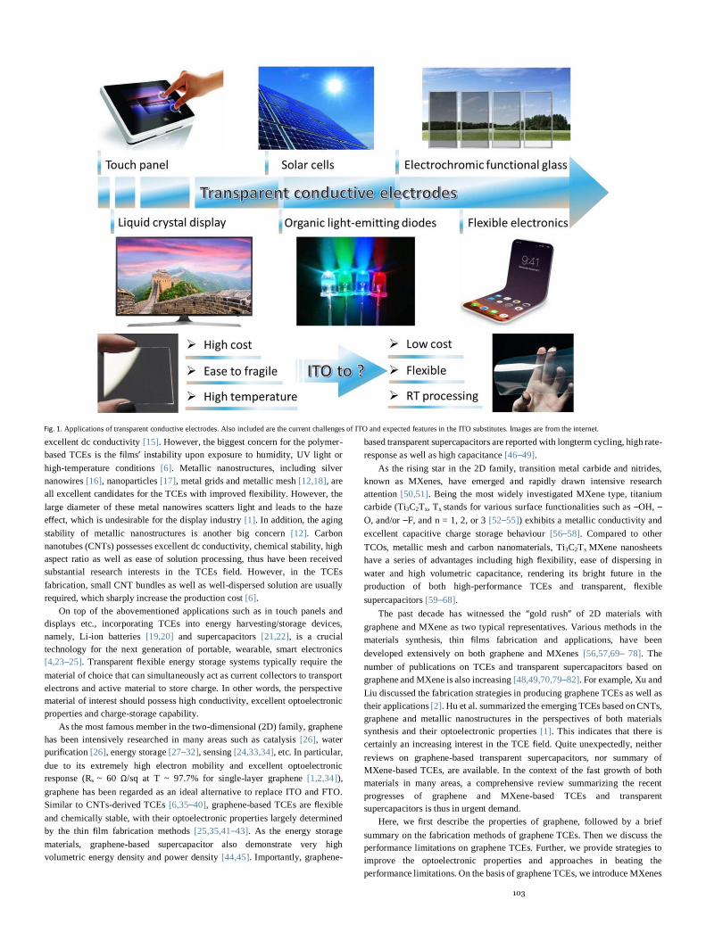
optoelectronic devices, as shown in Fig. 1 [1–4]. The global market for TCEs
was $4.8 billion in 2013, and soared to nearly $7.1 billion in 2018. Currently,
the majority of TCEs is consumed by the LCD and touch panel industry [5,6].
The dominant materials used today for TCEs are transparent conductive
oxides (TCOs) [7]. Among which tin-doped indium oxide (ITO) is the most
successful material in the commercial market and well-studied one in the
research labs [8]. Attributed to its extremely good optoelectronic properties,
such as low sheet resistance (Rs, 10– 100 Ω/sq) at high transmittance (T > 85%),
ITO-based TCEs have occupied a $5.1 billion market in 2017 with an expected
growth rate of 20%. Despite that, its intrinsic drawbacks cannot be ignored: (1)
The scarcity of indium leads to high cost of ITO production. (2) ITO-based
TCEs are quite fragile, limiting their further applications in the flexible
electronics. The susceptible to crack or fracture nature will deteriorate the ITO-
based TCEs performance, such as linearity and sensing accuracy when used as
an interfacing device [9]. Although by transferring (or sputtering) ITO films
from glass to a flexible polyethylene terephthalate (PET) substrate, and/or
optimizing the indium and tin ratio will improve the mechanical properties of
these TCEs, additional production cost is unavoidable. (3) Manufacturing ITO
needs hightemperature treatment, which complexes the production and
consumes significant energy. (4) The instability of ITO films in acid or base
media limits their application, such as in organic solar cells [10]. Another
widespread type of TCO, fluorine-doped tin oxide (FTO), also suffers from
similar drawbacks as ITO.
These main drawbacks of ITO and FTO have greatly stimulated the quest
of alternatives with better mechanical properties, comparable optoelectronic
properties and most importantly, at lower costs [6,11– 13]. Of particular interest
are paid on conducting polymers, such as poly(3,4-
ethylenedioxythiophene):poly(styrenesulfonate)
(PEDOT:PSS), polypyrrole, and polythiophene, etc. [14]. After a simple
chemical doping, these conducting polymer-based TCEs showcase
⁎ Corresponding author at: CRANN and AMBER Research Centers, Trinity College Dublin, Dublin 2, Ireland. E-mail addresses:
[email protected] (C.J. Zhang), [email protected] (V. Nicolosi).
103
Fig. 1. Applications of transparent conductive electrodes. Also included are the current challenges of ITO and expected features in the ITO substitutes. Images are from the internet.
excellent dc conductivity [15]. However, the biggest concern for the polymer-
based TCEs is the films’ instability upon exposure to humidity, UV light or
high-temperature conditions [6]. Metallic nanostructures, including silver
nanowires [16], nanoparticles [17], metal grids and metallic mesh [12,18], are
all excellent candidates for the TCEs with improved flexibility. However, the
large diameter of these metal nanowires scatters light and leads to the haze
effect, which is undesirable for the display industry [1]. In addition, the aging
stability of metallic nanostructures is another big concern [12]. Carbon
nanotubes (CNTs) possesses excellent dc conductivity, chemical stability, high
aspect ratio as well as ease of solution processing, thus have been received
substantial research interests in the TCEs field. However, in the TCEs
fabrication, small CNT bundles as well as well-dispersed solution are usually
required, which sharply increase the production cost [6].
On top of the abovementioned applications such as in touch panels and
displays etc., incorporating TCEs into energy harvesting/storage devices,
namely, Li-ion batteries [19,20] and supercapacitors [21,22], is a crucial
technology for the next generation of portable, wearable, smart electronics
[4,23–25]. Transparent flexible energy storage systems typically require the
material of choice that can simultaneously act as current collectors to transport
electrons and active material to store charge. In other words, the perspective
material of interest should possess high conductivity, excellent optoelectronic
properties and charge-storage capability.
As the most famous member in the two-dimensional (2D) family, graphene
has been intensively researched in many areas such as catalysis [26], water
purification [26], energy storage [27–32], sensing [24,33,34], etc. In particular,
due to its extremely high electron mobility and excellent optoelectronic
response (Rs ~ 60 Ω/sq at T ~ 97.7% for single-layer graphene [1,2,34]),
graphene has been regarded as an ideal alternative to replace ITO and FTO.
Similar to CNTs-derived TCEs [6,35–40], graphene-based TCEs are flexible
and chemically stable, with their optoelectronic properties largely determined
by the thin film fabrication methods [25,35,41–43]. As the energy storage
materials, graphene-based supercapacitor also demonstrate very high
volumetric energy density and power density [44,45]. Importantly, graphene-
based transparent supercapacitors are reported with longterm cycling, high rate-
response as well as high capacitance [46–49].
As the rising star in the 2D family, transition metal carbide and nitrides,
known as MXenes, have emerged and rapidly drawn intensive research
attention [50,51]. Being the most widely investigated MXene type, titanium
carbide (Ti3C2Tx, Tx stands for various surface functionalities such as –OH, –
O, and/or –F, and n = 1, 2, or 3 [52–55]) exhibits a metallic conductivity and
excellent capacitive charge storage behaviour [56–58]. Compared to other
TCOs, metallic mesh and carbon nanomaterials, Ti3C2Tx MXene nanosheets
have a series of advantages including high flexibility, ease of dispersing in
water and high volumetric capacitance, rendering its bright future in the
production of both high-performance TCEs and transparent, flexible
supercapacitors [59–68].
The past decade has witnessed the “gold rush” of 2D materials with
graphene and MXene as two typical representatives. Various methods in the
materials synthesis, thin films fabrication and applications, have been
developed extensively on both graphene and MXenes [56,57,69– 78]. The
number of publications on TCEs and transparent supercapacitors based on
graphene and MXene is also increasing [48,49,70,79–82]. For example, Xu and
Liu discussed the fabrication strategies in producing graphene TCEs as well as
their applications [2]. Hu et al. summarized the emerging TCEs based on CNTs,
graphene and metallic nanostructures in the perspectives of both materials
synthesis and their optoelectronic properties [1]. This indicates that there is
certainly an increasing interest in the TCE field. Quite unexpectedly, neither
reviews on graphene-based transparent supercapacitors, nor summary of
MXene-based TCEs, are available. In the context of the fast growth of both
materials in many areas, a comprehensive review summarizing the recent
progresses of graphene and MXene-based TCEs and transparent
supercapacitors is thus in urgent demand.
Here, we first describe the properties of graphene, followed by a brief
summary on the fabrication methods of graphene TCEs. Then we discuss the
performance limitations on graphene TCEs. Further, we provide strategies to
improve the optoelectronic properties and approaches in beating the
performance limitations. On the basis of graphene TCEs, we introduce MXenes

104
and discuss their synthesis and properties in brief. Then, we review the
progresses on MXene-based TCEs, focusing on the thin film fabrication
methods as well as limitations. Metrics on the charge storage properties are
proposed using Ti3C2Tx MXene TCE as a typical example. Using the figure of
merits (both capacitive, FoMc, and electrical, FoMe), we are able to compare
the optoelectronic properties of a vast of TCEs, and electrochemical responses
of various transparent supercapacitors. Finally, the challenges and perspectives
in these fields are also discussed. It is thus assured that the TCEs will continue
to grow and play an important role in future transparent, flexible electronics.
2. Graphene-based TCEs
2.1. Properties of graphene
Since the discovery in 2004 [83], the one-atom-thick graphene has aroused
extensive research interests continuously and thus intrigued a “gold rush”
worldwide. Ideally, graphene is defined as the carbon monolayer packed into a
2D honeycomb with a sp2-hybridized configuration [84]. The high-quality
graphene produced by the mechanical cleavage method showcases many
unique properties, including extremely high electron mobility of 2.5 × 105 cm2
V-1 s-1 [85], very high thermal conductivity (> 3000 W m-1 K-1) [86] and
mechanical strength of 130 GPa [87], etc. A pure, single-layered graphene
nanosheet is a semiconductor, demonstrating a bandgap of 0 eV [83] and a very
high Fermi velocity (vF = 2.5 × 10⁶ m s-1), due to electrons delocalized on the
sheets [88]. Detailed properties of monolayer graphene and comparison to its
allotropes can be found in Table 1. Notably, graphene monolayer is transparent
with the optical absorption of 2.3% [89]. Therefore, for the few-layered
graphene, the transmittance varies as T ~ 100-2.3N (%), where N is the number
of layers [90]. Despite that, for the graphene-like materials [91] obtained
through other techniques (Fig. 2), such as liquid-phase exfoliation [92,93],
oxidation/reduction of graphene oxide [94], chemical vapour deposition (CVD)
[95–98], etc. [99,100], the supreme characteristics have not been observed yet
[89]. Consequently, compromised optoelectronic properties are typically
experienced in these lower-quality graphene-based TCEs. This highlights the
crucial importance of both graphene synthesis and thin film fabrication
strategies.
In general, producing pristine graphene with minimum defects on the
mono- (or few) layers, followed by compacting the nanosheets into a
continuous network, are two critical steps in fabricating highperformance
graphene-based TCEs. This requires elaborate route design from the material
synthesis to TCE fabrication. While mechanical (or micromechanical) cleavage
of natural graphite can give large size, high-quality graphene flakes, however,
the low yield of graphene coupled with the film-transfer procedure significantly
hinder this
Table 1
Fig. 2. Typical routes to graphene synthesis. Each route is evaluated in five aspects, including
graphene quality (G), cost effective (C, a lower value suggests a higher production cost),
scalability (S), purity (P) and yield (Y) of the overall production process. Reprinted with
permission from Ref. [101]. Copyright 2014 Springer Nature.
method from mass production [89,102]. On the other hand, by choosing suitable
solvents, natural graphite can be directly exfoliated into defects-free graphene
dispersions (non-aqueous [93] or aqueous [103]) upon sonication [92,104] or
shear-mixing [93]. Nevertheless, controlling the layer number of the exfoliated
graphene while improving the portion of monolayers have proven to be
difficult/timeconsuming [105]. Fig. 2 compares various synthesis routes in
terms of quality (G), cost (C), scalability (S), purity (P) and yield (Y) of the
overall production process [101]. Of particular interest must be paid is the
chemical oxidation-reduction approach, which gives a high yield of reduced
graphene oxide with plenty of defects, both intrinsically (edges and
deformations) and extrinsically (O- and H-containing groups) [101]. While
excellent reviews on the roadmap of graphene covering electronic structure,
modelling, synthesis, devices, etc. are available [1,2,84], we will focus on the
fabrication of graphene-based TCEs from various methods as well as the
comparison of their optoelectronic properties.
A comparison of graphene properties to other carbonaceous materials. Reprinted with permission from Ref. [101]. Copyright 2014 Springer Nature.
Properties Graphene Carbon nanotube Fullerene graphite
Dimensions 2 1 0 3
Hybridization sp2 Mostly sp2 Mostly sp2 sp2
Hardness Highest (for single layer) High High High
Tenacity Flexible, elastic Flexible, elastic Elastic Flexible, non-elastic
Experimental SSA (m2 g-1) ~ 1500 ~ 1300 80–90 ~ 10–20
Electrical conductivity (S cm-1) ~ 2000 Structure-dependent 10-10 Anisotropic: 2–3 × 10⁴a, 6b
Thermal conductivity (W m-1 K-1) 4840–5300 3500 0.4 Anisotropic: 1500–2000a, 5–10b
a a direction b
c direction.
105
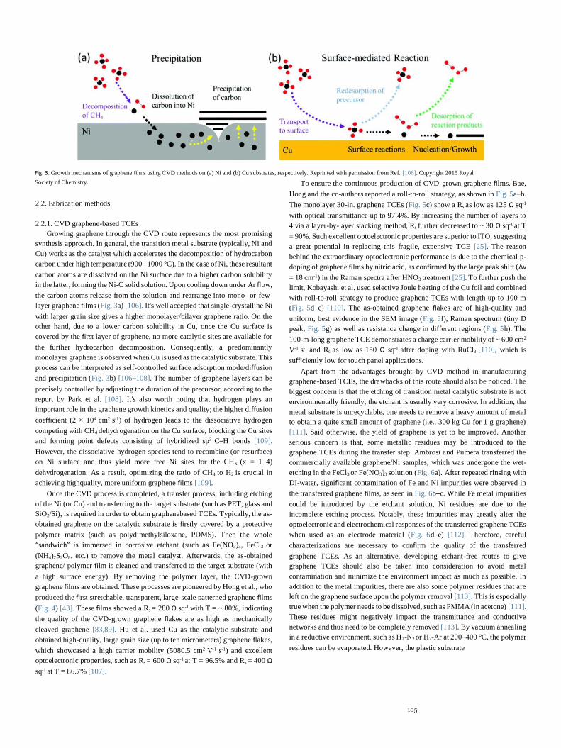
Fig. 3. Growth mechanisms of graphene films using CVD methods on (a) Ni and (b) Cu substrates, respectively. Reprinted with permission from Ref. [106]. Copyright 2015 Royal
Society of Chemistry.
2.2. Fabrication methods
2.2.1. CVD graphene-based TCEs
Growing graphene through the CVD route represents the most promising
synthesis approach. In general, the transition metal substrate (typically, Ni and
Cu) works as the catalyst which accelerates the decomposition of hydrocarbon
carbon under high temperature (900– 1000 °C). In the case of Ni, these resultant
carbon atoms are dissolved on the Ni surface due to a higher carbon solubility
in the latter, forming the Ni-C solid solution. Upon cooling down under Ar flow,
the carbon atoms release from the solution and rearrange into mono- or few-
layer graphene films (Fig. 3a) [106]. It's well accepted that single-crystalline Ni
with larger grain size gives a higher monolayer/bilayer graphene ratio. On the
other hand, due to a lower carbon solubility in Cu, once the Cu surface is
covered by the first layer of graphene, no more catalytic sites are available for
the further hydrocarbon decomposition. Consequently, a predominantly
monolayer graphene is observed when Cu is used as the catalytic substrate. This
process can be interpreted as self-controlled surface adsorption mode/diffusion
and precipitation (Fig. 3b) [106–108]. The number of graphene layers can be
precisely controlled by adjusting the duration of the precursor, according to the
report by Park et al. [108]. It's also worth noting that hydrogen plays an
important role in the graphene growth kinetics and quality; the higher diffusion
coefficient (2 × 104 cm2 s-1) of hydrogen leads to the dissociative hydrogen
competing with CH4 dehydrogenation on the Cu surface, blocking the Cu sites
and forming point defects consisting of hybridized sp3 C–H bonds [109].
However, the dissociative hydrogen species tend to recombine (or resurface)
on Ni surface and thus yield more free Ni sites for the CHx (x = 1–4)
dehydrogenation. As a result, optimizing the ratio of CH4 to H2 is crucial in
achieving highquality, more uniform graphene films [109].
Once the CVD process is completed, a transfer process, including etching
of the Ni (or Cu) and transferring to the target substrate (such as PET, glass and
SiO2/Si), is required in order to obtain graphenebased TCEs. Typically, the as-
obtained graphene on the catalytic substrate is firstly covered by a protective
polymer matrix (such as polydimethylsiloxane, PDMS). Then the whole
“sandwich” is immersed in corrosive etchant (such as Fe(NO3)3, FeCl3 or
(NH4)2S2O8, etc.) to remove the metal catalyst. Afterwards, the as-obtained
graphene/ polymer film is cleaned and transferred to the target substrate (with
a high surface energy). By removing the polymer layer, the CVD-grown
graphene films are obtained. These processes are pioneered by Hong et al., who
produced the first stretchable, transparent, large-scale patterned graphene films
(Fig. 4) [43]. These films showed a Rs = 280 Ω sq-1 with T = ~ 80%, indicating
the quality of the CVD-grown graphene flakes are as high as mechanically
cleaved graphene [83,89]. Hu et al. used Cu as the catalytic substrate and
obtained high-quality, large grain size (up to ten micrometers) graphene flakes,
which showcased a high carrier mobility (5080.5 cm2 V-1 s-1) and excellent
optoelectronic properties, such as Rs = 600 Ω sq-1 at T = 96.5% and Rs = 400 Ω
sq-1 at T = 86.7% [107].
To ensure the continuous production of CVD-grown graphene films, Bae,
Hong and the co-authors reported a roll-to-roll strategy, as shown in Fig. 5a–b.
The monolayer 30-in. graphene TCEs (Fig. 5c) show a Rs as low as 125 Ω sq-1
with optical transmittance up to 97.4%. By increasing the number of layers to
4 via a layer-by-layer stacking method, Rs further decreased to ~ 30 Ω sq-1 at T
= 90%. Such excellent optoelectronic properties are superior to ITO, suggesting
a great potential in replacing this fragile, expensive TCE [25]. The reason
behind the extraordinary optoelectronic performance is due to the chemical p-
doping of graphene films by nitric acid, as confirmed by the large peak shift (Δν
= 18 cm-1) in the Raman spectra after HNO3 treatment [25]. To further push the
limit, Kobayashi et al. used selective Joule heating of the Cu foil and combined
with roll-to-roll strategy to produce graphene TCEs with length up to 100 m
(Fig. 5d–e) [110]. The as-obtained graphene flakes are of high-quality and
uniform, best evidence in the SEM image (Fig. 5f), Raman spectrum (tiny D
peak, Fig. 5g) as well as resistance change in different regions (Fig. 5h). The
100-m-long graphene TCE demonstrates a charge carrier mobility of ~ 600 cm2
V-1 s-1 and Rs as low as 150 Ω sq-1 after doping with RuCl3 [110], which is
sufficiently low for touch panel applications.
Apart from the advantages brought by CVD method in manufacturing
graphene-based TCEs, the drawbacks of this route should also be noticed. The
biggest concern is that the etching of transition metal catalytic substrate is not
environmentally friendly; the etchant is usually very corrosive. In addition, the
metal substrate is unrecyclable, one needs to remove a heavy amount of metal
to obtain a quite small amount of graphene (i.e., 300 kg Cu for 1 g graphene)
[111]. Said otherwise, the yield of graphene is yet to be improved. Another
serious concern is that, some metallic residues may be introduced to the
graphene TCEs during the transfer step. Ambrosi and Pumera transferred the
commercially available graphene/Ni samples, which was undergone the wet-
etching in the FeCl3 or Fe(NO3)3 solution (Fig. 6a). After repeated rinsing with
DI-water, significant contamination of Fe and Ni impurities were observed in
the transferred graphene films, as seen in Fig. 6b–c. While Fe metal impurities
could be introduced by the etchant solution, Ni residues are due to the
incomplete etching process. Notably, these impurities may greatly alter the
optoelectronic and electrochemical responses of the transferred graphene TCEs
when used as an electrode material (Fig. 6d–e) [112]. Therefore, careful
characterizations are necessary to confirm the quality of the transferred
graphene TCEs. As an alternative, developing etchant-free routes to give
graphene TCEs should also be taken into consideration to avoid metal
contamination and minimize the environment impact as much as possible. In
addition to the metal impurities, there are also some polymer residues that are
left on the graphene surface upon the polymer removal [113]. This is especially
true when the polymer needs to be dissolved, such as PMMA (in acetone) [111].
These residues might negatively impact the transmittance and conductive
networks and thus need to be completely removed [113]. By vacuum annealing
in a reductive environment, such as H2-N2 or H2-Ar at 200–400 °C, the polymer
residues can be evaporated. However, the plastic substrate

106
Fig. 4. (a–c) Schematic of transferring graphene films onto the target substrate. (a) Synthesis of pattered graphene films on thin Ni layers. Etching of Ni using (b) FeCl3 (or HCl) and (c) HF (or buffered
oxide etchant, BOE) and transferring of graphene films. (d) A floating graphene film after etching Ni layer in FeCl3 aq. The film can be directly transfer to any other substrates by direct contact with the
substrate. (e) The graphene films on the PDMS substrate is transparent and flexible. Reprinted with permission from Ref. [43]. Copyright 2009 Springer Nature.
Fig. 5. (a) Schematic of the roll-to-roll production of CVD-grown graphene TCE. (b) Roll-to-roll transfer of graphene films from a thermal release tape to a PET film at 120 °C. (c) A transparent ultralarge-
area graphene film transferred on a 35-in. PET sheet. Reprinted with permission from Ref. [25]. Copyright 2010 Springer Nature. (d) Schematic of 100 m graphene TCE production. Step 1: continuous
roll-to-roll CVD system using selective Joule heating to heat a Cu foil suspended between two current-feeding electrode rollers to ~ 1000 °C to grow graphene. Step 2: reverse gravure coating of a
photocurable epoxy resin onto a PET film and bonding to the graphene/copper foil, followed by curing of the epoxy resin. Step 3: spray etching of the copper foil with a CuCl2 solution. Step 4: structure
of the fabricated graphene/epoxy/PET film. (e) Photograph of the graphene/epoxy/PET roll before doping. The widths of the graphene/epoxy and base PET film are 210 mm and 230 mm, respectively.
(f) SEM image and (g) Raman spectrum of the graphene film. (h) Rs of the graphene/epoxy/PET film along the longitudinal direction measured every 1 m. The horizontal dashed lines represent the
averaged data in 0–52 m and 52–100 m regions. Reprinted with permission from Ref. [110]. Copyright 2013 American Institute of Physics (AIP).

107
Fig. 6. (a) Schematic of transferring of the CVD-grown graphene film from Ni substrate to glass. (b) Scanning transmission electron microscopy (STEM) of graphene films loaded onto Cu grids after
many times DI-water washes. (c) Energy dispersive (EDX) analysis confirmed the presence of plenty of Cu and Fe residual. (d) Representative cyclic voltammograms (CVs) performed in phosphate
buffered solution (pH 7.2) in the presence of 10 mM cumene hydroperoxide (CHP) and using EPPG (black line), BPPG (blue line), GC (black dotted line) and transferred CVD graphene (red line). (e)
CVs (after 100 potential scans) performed in 0.1 M NaOH solution using clean Ni foil (black line) and transferred CVD graphene (blue line).
Reprinted with permission from Ref. [112]. Copyright 2014 Royal Society of Chemistry.
cannot bear such a high temperature [2]. Other routes, such as inserting an
additional buffer layer (2-(diphenylphosphory)spirofluorene, SPPO1)-which
has a high solubility in the solvent- between graphene and PMMA, or simply
choosing conductive polymer (such as PEDOT:PSS) as the supporting layer and
target substrate, residuefree graphene TCEs can be achieved [113]. Despite all
these exciting progresses, developing transfer-free methods and growing
graphene films directly on the target substrate (such as dielectric ones) [114],
would greatly simplify the steps, give high-quality graphene TCEs without
polymer or metal residues, and thus should be encouraged in the future.
2.2.2. Reduced graphene oxide-based TCEs
Aside from CVD-derived graphene, depositing graphite oxide (GO)
nanosheets followed by reduction is another promising route to fabricate
graphene-based TCEs. The quality of the GO flakes and thin film fabrication
methods largely determine the optoelectronic properties of the resultant
graphene TCEs. This highlights the importance of GO synthesis as well as the
solution processing of GO.
The most common route to GO is by aggressively oxidizing the natural
graphite using a mixture of sodium nitrate, potassium permanganate and
concentrated sulfuric acid [77,91,115–119]. This process is widely known as
the modified Hummers method, proposed by Hummers and Offerman [120].
Once being oxidized, the interlayer spacing of the GO increases to ~ 1.2 nm, ~
3 time wider than that of natural graphite (0.34 nm) [91,99,115,120]. The
expanded interlayer spacing allows the liquid-phase exfoliation of graphite
oxide into mono- or few-layer GO nanosheets under the assistance of ultrasonic
agitation or thermal expansion [2,32,100]. The as-obtained GO sheets are
decorated with plenty of negatively-charged groups, such as hydroxyl and
epoxy groups on the basal planes while carboxyl groups on the edges,
respectively [2,120]. These groups endow the GO sheets with a very good
hydrophilicity. Thus, GO can be electrostatically stable in the form of colloidal
aqueous solution without the need of surfactant [121,122]. This brings
significant advantages in solution processing of GO dispersion, such as spray-
coating [123], spin-casting [116], dipcoating [116], electrophoretic deposition
[124], Langmuir-Blodgett assembly (including layer-by-layer, LBL) [125],
vacuum filtration [126], etc., based on which transparent GO films are obtained
[115]. Among these methods, spin-coating gives compact, uniform GO films on
a flat substrate [116]. To achieve this, typically a concentrate GO solution is
required and placed on the substrate, followed by rotation. The film thickness
can be controlled by varying the speed, duration and concentration of the
solution [127,128]. On the other hand, spraying the GO solution, regardless of
the concentration, can control the thickness of the resultant GO films more
efficiently by varying the number of paths [123]. While dip-coating requires
multiple steps, thus, time-consuming, to achieve GO films, electrophoretic
deposition allows a fast fabrication rate [124]. However, the substrate is limited
to the conductive ones, and exclude plastic, such as PET as a result. For the
vacuum filtration, GO nanosheets are forced to compactly stack on the cellulose
ester membrane and thus the network is formed. Additional step is that the
membrane has to be removed [99], leaving the concern that there are some
cellulose residues, similar as the polymer removal in the CVD-grown graphene
transfer process [114]. For the LangmuirBlodgett and LBL assembly, GO film
thickness can be effectively and easily manipulated [125]. It's worth mentioning
that crosslinking agents, with positively charge species, need to be added to
counteract the strong electrostatic repulsion between the GO sheets [2]. This

108
method allows the production of continuous and uniform GO films on arbitrary
substrates, including flexible ones on a large scale.
Once the GO films are prepared, restore the sp2 C–C bonds are necessary in
order to achieve conductive films. The reduced GO, usually known as rGO, is
obtained by thermal or chemical reduction. Generally, thermal reduction is
more effective in removing the surface groups (such as -OH, -O, and -COOH)
than the chemical reduction route [2]. By heating up the GO films at 400–1100
°C, all these oxygencontaining groups are removed in the form of CO2 and
CO, resulting in much improved electronic conductivity in rGO [32,116].
However, in this temperature range, plastic substrate can’t be used to support
the rGO film. On the other hand, the chemical reduction route employs a
reductive agent, such as hydrazine [31], hydrogen iodide (HI) [115] and
NaBH4 [129] to remove the surface functionalities on the GO nanosheets.
Despite a mass production can be achieved, the chemical reduction process is
quite dangerous and generates lots of environmental unfriendly wastes
[130,131]. Great caution must be taken when chemically converting GO to
rGO. Besides, this aggressive route also introduces plenty of defects on the
basal planes, which compromises the optoelectronic properties of the rGO-
based TCEs [120]. As an alternative, using the in-situ formed hydrogen was
reported as an efficient reducing agent to obtain rGO in an eco-friendly
manner [127].
Chhowalla et al. performed the pioneering work on fabricating the rGO
TCEs through vacuum-filtration, followed by a combination of hydrazine
vapour exposure and low-temperature annealing treatments, as shown in Fig.
7a–c [126]. The films showcased a lowest Rs of 105 kΩ sq-1 at T of ~ 58%. Later,
Dai et al. produced graphene films through LB method (Fig. 7d–f), which
showcased Rs of 8 kΩ sq-1 at T of ~ 83%. The graphene films were obtained by
exfoliation-reintercalation-expansion strategy [125]. By spin-casting the GO
solution followed by hydrazine vapour reduction at 400 °C or graphitization at
1100 °C, Chen et al. were able to produce rGO-based TCEs with Rs of 100–
1000 Ω sq-1 at T of ~ 80% [116]. The rGO films that Cheng et al. fabricated
based on large-area GO nanosheets also exhibited quite similar results,
including Rs of 840 Ω sq-1 at T of ~ 78% [115]. To further decrease Rs
Table 2 Fabrication and optoelectronic properties of various graphene-based TCEs.
Method Reduction Modification T (@ 550 nm)
Rs (Ω/sq) Refs.
Filtration HI acid HNO3 bath doping 59% 565 [136]
L-B assembly / / 83% 8k [125]
L-B assembly HI acid HNO3 bath doping 91% 1100 [137]
Spin-coating Thermal / 80% 870 [138]
Spin-coating H2 from Al etching
Ag nanowires
hybridization 89% 74 ± 7 [127]
Dip-coating + LBL
Thermal CTAB N2-dopeda 60% 298 [139]
Rod coating Metallic Sn / 75% 6.7k [140]
a Cetyltrimethylammonium bromide (CTAB).
while maintain T of the films, rGO can be hybridized with other nanostructures,
such as CNTs [132,133], metallic grids [134], PEDOT:PSS [113], Cu
nanowires [128] and Ag nanowires [120,135], etc. [2,133]. These approaches
will be discussed in detail in Section 2.4.2. Typical details of rGO-based TCEs,
including GO synthesis, modification as well as the optoelectronic properties of
the films, are summarized in Table 2.
2.2.3. Graphene solution-based TCEs
Despite great progresses have been achieved on the mass production of GO
and solution processing techniques, the usage of environmentally unfriendly
chemicals as well as the introduction of destructive network severely limit the
application of rGO TCE based on GO solution [1,2]. For the sake of potentially
large-scale production, one needs to develop high-quality graphene flakes
suspended in dispersion, which is compatible with the aforementioned solution
processing
Fig. 7. (a–c) Thin films of solution-processed GO. Optical images of GO thin films on (a) filtration membrane before transfer to (b) glass and (c) PET substrates. Reprinted with permission from Ref.
[126]. Copyright 2008 Springer Nature. (d–f) Characterizations of graphene sheet (GS) films fabricated from Langmuir–Blodgett (LB) method. (d) A photograph of a two-layer GC-LB film on quartz

109
with part of it left clear. The scale bar is 10 mm. (e) Transparency spectra of one- (black curve), two- (red curve) and three-layer (green curve) GS-LB films. The transparency was defined as the
transmittance at a wavelength of 1000 nm. (f) Resistance (red) and transmittance (blue) of one-, two- and three-layer LB films. Permission from Ref. [125]. Copyright 2008 Springer Nature.
Fig. 8. (a) Importance of a good solvent in stabilizing the as-exfoliated 2D nanosheets. (b) Dispersed graphene concentration as a function of solvent surface energy. Insets show the structures of NMP
(left) and DMF (right). (c) TEM images of graphene monolayer and multilayer respectively. (d) Histogram showing the distribution of graphene layer thicknesses. These graphene flakes in (c–d) are
exfoliated in NMP. (e–f) TEM images of surfactant-exfoliated flakes. The surfactant is sodium cholate (NaC). (g) Digitally filtered high-resolution image of a surfactant-exfoliated flake. Reprinted with
permission from Ref. [104]. Copyright 2013 American Chemical Society. (h) A Silverson model L5M high-shear mixer with mixing head in a 5 L beaker of graphene dispersion. (i–j) Close-up view of
a D = 32 mm mixing head (i) and a D = 16 mm mixing head with rotor (left) separated from stator. (k) Graphene– NMP dispersions produced by shear exfoliation. (l) TEM image of shear-exfoliated
graphene nanosheets and (m) histogram of graphene nanosheets by AFM on a surfactant-exfoliated sample. The presence of monolayers was confirmed by Raman characterization (inset). Reprinted
with permission from Ref. [93]. Copyright 2014 Springer Nature.
strategies, such as spin-coating, dip coating, spray-coating, and vacuum
filtration-transfer etc.
This means that graphite needs to be exfoliated into few-layer (or
monolayer) graphene in solvent. Such a top-down strategy is widely known as
liquid-phase exfoliation, LPE [92,104,141]. According to Coleman et al., the
concentration of graphene is thus maximized when the surface tension of the
solvent matches with the surface energy of graphite [92,104,105,142,143]. Fig.
8a shows the importance of the solvent. In good solvents, the nanosheets are
exfoliated and stabilized against re-aggregation. However, a bad solvent not
only yields a low concentration of graphene nanosheets, but also leads to the
quick sedimentation after a period of time during aging. As evidenced in Fig.
8b, graphite tends to give a maximum graphene nanosheets concentration in the
region of solvent surface energy ~ 65–75 mJ cm2 , falling into the range of
graphite surface energy [44,92,104,105,143]. Typically, NMP is the ideal
solvent for liquid-phase exfoliation of graphene, as nice flakes with a
predominantly 1–4 layers are obtained (Fig. 8c–d). However, for the potential
large-scale production, aqueous graphene solution is preferred, as it allows an
efficient, green production of graphene-based thin films, coatings, and devices,
etc. [84]. To achieve this, one needs to lower down the surface tension of water
either using surfactant or polymer, and drags the value into the optimum region,
that is, the region with surface tension roughly equals to the surface energy of
graphite. Sodium cholate (NaC) has been proved as an efficient surfactant in
producing high-quality graphene dispersions, as seen in Fig. 8e–g [103,144].
By controlling the critical factors, such as the NaC/graphite ratio, initial
concentration, sonication time, power and frequency, as well as centrifugation
parameters (speed, time, etc.), an aqueous dispersion enriched with high-quality
graphene flakes can be obtained [103,104,144]. Removal of the surfactant is
necessary, and can be realized by repeated washing with DI-water, or vacuum
annealing of the graphene-based products [42]. Beside the NaC, graphite can
be also exfoliated under the assistance of household detergent [145] or
polymers (such as poly(ethylene oxide)), or poly(ethylene glycol), PEG [146].
The former needs to combine with turbulence such as kitchen blender [145].
Indeed, when shear mixing graphite particles in suitable solvent/surfactant, a
large-scale quantity of high-quality graphene dispersions can be achieved,
according to Coleman et al. [93].
With high-quality graphene dispersions, one can readily prepare graphene
thin films by either spray-coating or vacuum filtration, followed by transferring
to the target substrate and dissolving the ester membrane with acetone [126].
For instance, Coleman et al. demonstrated flexible graphene-TCEs from
exfoliated graphene dispersions stabilized by surfactant. The as-obtained films,
which were annealed at 200–1000 °C under H2/Ar flow for 2 h, showcased
conductivities of up to ~104 S m-1 coupled with T ~ 90% [42]. Such a dc
conductivity is also comparable to the best TCE produced from chemically-
modified graphene [147]. Graphene can also be exfoliated with the aid of
Nafion, forming a stable water/ethanol solution [148]. After a low annealing
temperature (250 °C for 2 h) under vacuum, the resulting graphene films
demonstrate a Rs of 2.86 kΩ sq-1 and a T of 84% at 550 nm [148]. Jo et al.
exfoliated large size (> 1 µm) graphene nanosheets assisted by PEG. After
treating with nitric acid and thionyl chloride (SOCl2), the graphene TCEs show
a Rs of 300 Ω sq-1 and a T of 74% [146]. While these sheet resistances from

110
exfoliated graphene dispersions are reasonable good, however, it's still
relatively high to find application for certain areas such as displays and solar
cells, where ~ 10 Ω sq-1 is typically required [1]. Generally, comparing to
CVDgrown graphene TCEs, liquid-phase exfoliated graphene TCEs showcase
higher Rs at similar T. This can be attributed to the much smaller size of
graphene sheets after exfoliation. Smaller size means more boundaries and
lower charge carrier mobility among the network, leading to inevitably poorer
optoelectronic properties than the network with larger nanosheets. Continued
improvements on the crucial aspects, such as increasing the nanosheet size,
reducing defects, enhancing the electrical contacts on the junctions, as well as
increasing the charge carrier number through doping are routes to boost the
overall performance as TCEs. It could be anticipated that, in the next couple of
years, some commercial products will be available, provided that substantial
enhancement on the optoelectronic performance will be achieved.
2.3. Evaluation metrics of graphene TCEs
2.3.1. Trade-off between T and Rs
Ideal TCE should possess both high T across the UV–vis-NIR spectrum and
low Rs. In practical, the absorbance at 550 nm is defined as T in the UV–vis
spectrum of the film, while Rs can be obtained by a four-point (or two-point)
probe method. Increasing the film thickness will reduce the Rs at the cost of T.
In other words, there is a trade-off between these two parameters. T is linked to
the optical conductivity of the film, while Rs is related to the intrinsic electronic
conductivity of graphene. Importantly, Rs is thickness-dependant; different
thickness leads to different Rs and T, making the direct comparison difficult.
Therefore, it's necessary to put up with a performance metrics that can evaluate
the optoelectronic properties of the graphene TCEs easily.
Among some variations, the one that Coleman et al. proposed, ratio of dc
electrical conductivity (σdc) to optical conductivity (σop), so-called electrical
figure of merit (FoMe = σdc/σop), is widely accepted
[15,16,23,35,37,38,41,42,132,149,150]. The FoMe can be obtained through the
following Eq. (1):
188.5 σ
op −2
T = (1 + )
Rs σdc (1)
To make the above equation valid, several requirements need to be met (1)
the wavelength of the incident light is larger than the film thickness and (2) the
fraction of reflected light is much less than the absorbance [6]. For most of the
TCEs, these two conditions are usually met, thus Eq. (1) is frequently employed
to estimate the optoelectronic properties of the TCEs. Simply, one needs to
measure T and Rs for a given film and calculates the FoMe of the film at this
thickness (or T) according to Eq. (1). A higher FoMe indicates better
optoelectronic properties, and thus the corresponding film can be used in the
applications that require higher FoMe values. For example, the touch panel
requires T > 85% and Rs < 500 Ω sq-1 while liquid crystal display (LCD) screen
T > 85% and Rs < 100 Ω sq-1. According to Eq. (1), the minimum FoMe is
calculated to be 4.5 in touch panel and 22.3 in LCD, respectively. Table 3 lists
the specific requirements of TCEs in different applications.
Since the optoelectronic properties of graphene-TCEs are related to the
thickness, thus knowing the film thickness is of importance. For the
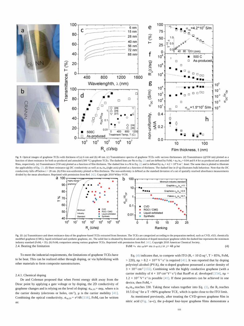
homogeneous opaque graphene films (T < 70%, Fig. 9a), the thickness can be
measured accurately through atomic force microscopy (AFM) or contact
profilometry. However, for the highly transparent films with T > 90% (Fig. 9b),
the thickness is beyond the resolution of contact profilometry. Instead, it can be
predicted through Eq. (2), if the optical conductivity, σop, is known:
T = [1 + 188.5σ top
]−2 (2)
By measuring T (@550 nm) of the films (Fig. 9c), the thickness can be thus
obtained by calculation.
2.3.2. Percolation problems
Fig. 9d plots T vs Rs of graphene TCEs [42]. Also included is the dashed
line by plotting Eq. (1). Clearly, in the films with T < 70%, the (T, Rs) points
are roughly on the dashed line. However, in the region with T > 80%, obvious
deviation is found; thinning down the film thickness leads to dramatically
increased Rs. This issue is known as percolation effect, which is reflected by the
deviation of bulk-like behaviour in the T vs Rs and Rs vs t plot in the highly
transparent region (dashed line in Fig. 9d–f).
In principle, in the graphene TCEs, charge carriers flow along an individual
nanosheet and then jump to another on the sheets boundaries. Therefore, the
sheet resistance is a sum of junction resistance and intrinsic resistance from the
nanosheets themselves. As charge carriers delocalize over the entire sheet and
travel thousands of interatomic distances without scattering, individual
graphene sheets showcase a very high Fermi velocity vF = 106 m/s, resulting in
impressively high inplane conductivities [151]. Said otherwise, the junction
resistance and therefore, the interflake tunnelling barriers largely determines the
optoelectronic performance in the graphene-based TCEs. According to the 2D
percolation theory, the percolation threshold (Nc) can be described through the
following Eq. (2):
Nc = 4.2362πLs2 ≈ 1/L (3)
where Ls and L are the individual length and the aspect ratio of the graphene,
respectively [152]. For typical exfoliated graphene flakes (layer number 1–10,
Fig. 8m), the aspect ratio (L) is much lower than that of CNTs, resulting in a
much higher percolation threshold. This means that the surface coverage to
form a path and conduct the charge carriers is higher. However, in the highly
transparent graphene TCEs (T > 80%), the film thickness typically falls below
Nc, leading to a nonuniform surface coverage and resulting in dramatically
increased sheet resistances. Consequently, percolation problems are
encountered.
2.3.3. Theoretical limitation on graphene-TCEs
De and Coleman compared the optoelectronic properties of graphene-based
TCEs by collecting T and Rs from various published papers (Fig. 10a), and
calculated FoMe using Eq. (1) [41]. Fig. 10b summarizes the FoMe data. For the
solution-exfoliated graphene, except the rGO films produced via spin-coating
followed by hightemperature graphitization in vacuum [116], FoMe ~ 0.7 may
be close to the limiting value, although this value depends on the lateral flake
Table 3 The specific requirements of TCEs in various practical applications. Reprinted with permission
from Ref. [6]. Copyright 2016 American Chemical Society.
Application T (%) Rs (Ω sq-1)
σdc/σop (FoMe)
Touch panel 85 500 4.5
LCD screen 85 100 22.3
OLED display 90 50 69.7
Photovoltaic electrode 90 10 348
size. For the CVD-grown graphene films, a highest FoMe (= 11) is observed.
This can be explained that the interflake junctions, similar as junctions in the
CNT networks, is much less in the quasi-continuous CVD grown films than the
solution processed films [41].
The reasons for the relatively low FoMe values, in spite of the high DC
conductivities in the graphitic films, are intriguing. For the films that Cai et al.
and Li et al. prepared, σdc reached 2 × 10⁶ S m-1 [153,154]. However, the σop in
these graphitic films also reached 1.8 × 10⁵ S m-1. Therefore, it is this high
optical conductivity that is responsible for the low FoMe.
111
2.4. Beating the limitation
To meet the industrial requirements, the limitations of graphene TCEs have
to be beat. This can be realized either through doping, or via hybridizing with
other materials to form composite nanostructures.
2.4.1. Chemical doping
De and Coleman proposed that when Fermi energy shift away from the
Dirac point by applying a gate voltage or by doping, the 2D conductivity of
graphene changes and is relying on the level of doping: σdc,2D = neµ, where n is
the carrier density (electrons or holes, cm-2), µ is the carrier mobility [41].
Combining the optical conductivity, σop,2D = e2/4ℏ [116], FoMe can be written
as:
FoM =e σdc op/σ= σdc D op D,2 /σ ,2= 4ℏ μ/ne (4)
Eq. (4) indicates that, to compete with ITO (Rs < 10 Ω sq-1, T > 85%, FoMe
> 220), nµ > 8.2 × 10¹⁶ V-1 s-1 is required [41]. It was reported that by doping
polyvinyl alcohol (PVA), the n-doped graphene possessed a carrier density of
3 × 1012 cm-2 [155]. Combining with the highly conductive graphene (with a
carrier mobility of 4 × 104 cm2 V-1 s-1) that Ruoff et al. developed [154], nµ =
1.2 × 10¹⁷ V-1 s-1 is possible [41]. If these parameters can be achieved in one
device, then FoMe =
σdc/σop reaches 330. Taking these values together into Eq. (1), the Rs reaches
10.5 Ω sq-1 for a T =90% graphene TCE, which is quite close to the ITO limit.
As mentioned previously, after treating the CVD-grown graphene film in
nitric acid (Fig. 5a–c), the p-doped four-layer graphene films demonstrate a
Fig. 9. Optical images of graphene TCEs with thickness of (a) 6 nm and (b) 40 nm. (c) Transmittance spectra of graphene TCEs with var ious thicknesses. (d) Transmittance (@550 nm) plotted as a
function of sheet resistance for both as-produced and annealed (500 °C) graphene TCEs. The dashed lines are fits to Eq. (1) and are defined by FoMe = σdc/σop = 0.04 and 0.4 for as-produced and annealed
films, respectively. (e) Transmittance (550 nm) plotted as a function of film thickness. The dashed line is a fit to Eq. (2) and is defined by σop = 4.2 × 10⁴ S m-1. Inset: The same data is plotted to illustrate
the applicability of Eq. (2). (f) Sheet resistance (g) DC conductivity as well as σdc/σop (right axis) plotted as a function of thickness. The dashed line in (f–g) illustrates bulk behaviour. Note that the DC
conductivity falls off below t = 20 nm. (h) Film non-uniformity plotted vs film thickness. The non-uniformity is defined as the standard deviation of a set of spatially resolved absorbance measurements
divided by the mean absorbance. Reprinted with permission from Ref. [42]. Copyright 2010 Wiley-VCH.
Fig. 10. (a) Transmittance and sheet resistance data of the graphene-based TCEs extracted from literature. The TCEs are categorized according to the preparation method, such as CVD, rGO, chemically
modified graphene (CMG), liquid exfoliated and synthetic graphene, etc. The solid line is obtained by theoretical calculation of doped monolayer graphene while the dashed line represents the minimum
industry standard (FoMe = 35). (b) FoMe comparison among various graphene TCEs. Reprinted with permission from Ref. [41]. Copyright 2010 American Chemical Society.
112
high T = 90% and a Rs = 30 Ω sq-1, indicating a FoMe as high as 116 according
to Eq. (1) [25]. Similarly, the AuCl3-doped graphene reported by Im et al. also
demonstrate a much decreased Rs (~ 70 Ω sq-1) compared to the pristine
graphene TCE (~ 890 Ω sq-1) [156]. In a recent study, the five-layer CVD-grown
graphene doped by thionyl chloride (SOCl2) exhibits an almost three-fold
decrease in the Rs (25 Ω sq-1) with T = 87% (FoMe = 104) [157], suggesting the
chemical doping method is universal. This is attributed to an increased hole
concentration due to the covalent attachment of electron acceptor chlorine
atoms at graphene defect sites with hydroxyl and carboxyl functionalities [157–
159]. Therefore, chemical doping (p type of n type) of CVD-grown graphene
is an effective approach to boost the optoelectronic properties of graphene
TCEs, which hold a great promise in replacing ITO in the near future.
2.4.2. Hybridizing with nanomaterials
By fabricating graphene-based composite nanostructures, the
optoelectronic properties of graphene TCEs can also be substantially improved
and outperformed the theoretical result. For example, addition of small amount
(3%) graphene to CNTs network, followed by chemical doping (nitric acid
treatment) was proved to be quite effective in enhancing the optoelectronic
performance, as Rs decreases to 100 Ω sq-1 at T = 80%, corresponding to FoMe
= 18 [132]. Lee et al. reported PEDOT:PSS-doped graphene TCEs. While the
pristine graphene exhibits a Rs of 214 ± 22 Ω sq-1, the composite showcases ~
80 Ω sq-1 at T = 84%, indicating a FoMe of 26 [113]. Blom et al. sprayed the
graphene nanosheets on top of silver nanowires films (Fig. 11a) [160]. It's found
that the electrochemically-exfoliated graphene nanosheets are quite efficient in
reducing the sheet resistance of Ag nanowires, improving the surface roughness
as well as enhancing the Ag nanowires ambient stability, as seen in Fig. 11b.
Consequently, the hybrid Ag/graphene TCEs displays a sheet resistance of ~
13.7 Ω sq-1 at T = 80%, an indicative of FoMe = 117 (Fig. 11c) [160]. On the
other hand, by compositing rGO platelet with Cu nanowires, synergistic effects
can happen; the Cu nanowires can decrease or eliminate the platelet-platelet
junction resistance, while the overlapped and continuous rGO films can bridge
initially segregated Cu nanowires and eliminate the empty spaces (Fig. 11d)
[128]. As a result, the hybrid films display Rs of 34 ± 2.6 Ω sq-1 at T = 80% (Fig.
11e) [128]. Importantly, Tour et al. used a photolithography method to achieve
metal grids (Au, Cu, Al) on the substrate, then transferred a graphene layer
prepared from CVD method on top of the metal grid, as shown in Fig. 11f–g.
The hybrid transparent Cu/graphene films demonstrate 3 ± 1 Ω sq-1 at T = 79%
and 22 ± 8 Ω sq-1 at T = 91% (FoMe = 177), while the Au/graphene TCE
showcased 20 ± 4 Ω sq-1 at T = 91% (FoMe = 195). To date, this is the highest
value in terms of FoMe for graphenebased TCEs (as shown in Fig. 11h),
indicating its great potential use in many applications [134]. There is no doubt
to believe that by further optimizing the composition in the hybrid films,
choosing other metal candidates as well as developing novel, facile thin-film
fabrication techniques, graphene-based TCEs can surpass the optoelectronic
properties of current dominate ITO electrodes, and find applications in many
areas.
3. MXene-based TCEs
3.1. Introduction on MXenes
Since the discovery of Ti3C2 in 2011, the family of transition metal carbides,
carbonitrides and nitrides, collectively referred to as MXenes, has quickly
expanded in many areas [50–52,56,161–168]. By selectively etching of A-
element layers from MAX precursor in aqueous fluoride-containing acidic
solutions, such as hydrofluoric acid, HF, or in-situ formed HF from lithium
fluoride and hydrochloric acid, LiF + HCl [51,52,55,71,169], or ammonium
hydrogen bifluoride (NH4HF2) [72,80,170], multi-layered (m-)MXene is thus
obtained. The abundant surface functional groups impart hydrophilicity to
MXenes [53]. When m-MXene is delaminated into monolayered or few-
layered nanosheets (d-MXene), a stable aqueous solution can be thus obtained,
due to the electrostatic force on the negatively charged MXene nanosheets
[57,72]. This allows a facile and environmentally friendly processing of the
MXene solution into any items, such as composites, coatings and devices.
Despite the presence of terminal surface groups, MXenes, especially the most
intensively studied titanium carbide MXene (Ti3C2Tx), showcase a metallic
conductivity as high as 9880 S cm-1 [171]. The excellent electronic conductivity
coupled with fast faradaic reactions result in impressive charge storage
property, so called pseudocapacitance, in the MXenes [54,172–175]. In
addition, monolayer MXene nanosheet is optical transparent, similar to the
analogue graphene [80]. Collectively, MXenes are quite promising for the
highperformance transparent conductive films and transparent supercapacitors.
Several excellent reviews detailed the synthesis, exfoliation, structure and
properties of MXenes [57,64,76,162,176]. Moreover, the applications of
MXenes, especially in energy storage devices such as supercapacitors, metal-
ion batteries/capacitors, have been extensively reported
[56,58,66,67,69,75,76,177–182]. Considering that the number of publications
on the MXenes grows enormously, we are not attempting to repeat the MXenes
synthesis, properties and energy storage applications exhaustively, rather, we
show some examples using MXenes as transparent conductive films.
3.2. Ti3C2Tx MXene-based TCEs
As mentioned previously, the percolation effect greatly limits the
fabrication of highly transparent thin films with low sheet resistance.
Developing advanced thin-film fabrication techniques as well as synthesizing
materials with a high DC conductivity can effectively solve this problem. In
this perspective, MXenes are ideal for the TCEs due to their metallic
conductivity and hydrophilicity.
Halim et al. performed the pioneer work on the fabrication of Ti3C2Tx
transparent films [80]. They sputter-deposited epitaxial Ti3AlC2 films on the
substrate, followed by selective etching of the Al element [80]. The as-obtained
epitaxial thin films were about 19 nm thick, corresponding to a T = 90% in the
visible-to-infrared range. Nevertheless, this route requires high-temperature for
the deposition (780 °C) and Al etching after the sputtering, which greatly limits
the scalable production. In other words, the film fabrication method must be
facile, environmentally green and cost effectively.
When m-Ti3C2Tx is intercalated with organic or water molecules, the
interlayer spacing is expanded, leading to weakened Van del Waals interactions
among the nanosheets [50,165]. Upon a bath sonication (under the inert gas) or
direct hand-shaking, the m-Ti3C2Tx delaminate into nanosheets aqueous
solution with a predominant monolayer distribution [58,72,173,183]. Similar to
GO, the d-Ti3C2Tx solution can be easily processed into Ti3C2Tx-based TCEs
with controlled thickness, thus, transparency, through spray-coating, spin-
coating or LBL techniques, etc. In addition, the ultrathin Ti3C2Tx nanosheets
interconnect and weave into a continuous conductive network, which endows
a good mechanical flexibility on the TCEs with less interflake tunnelling
barriers or junctions.
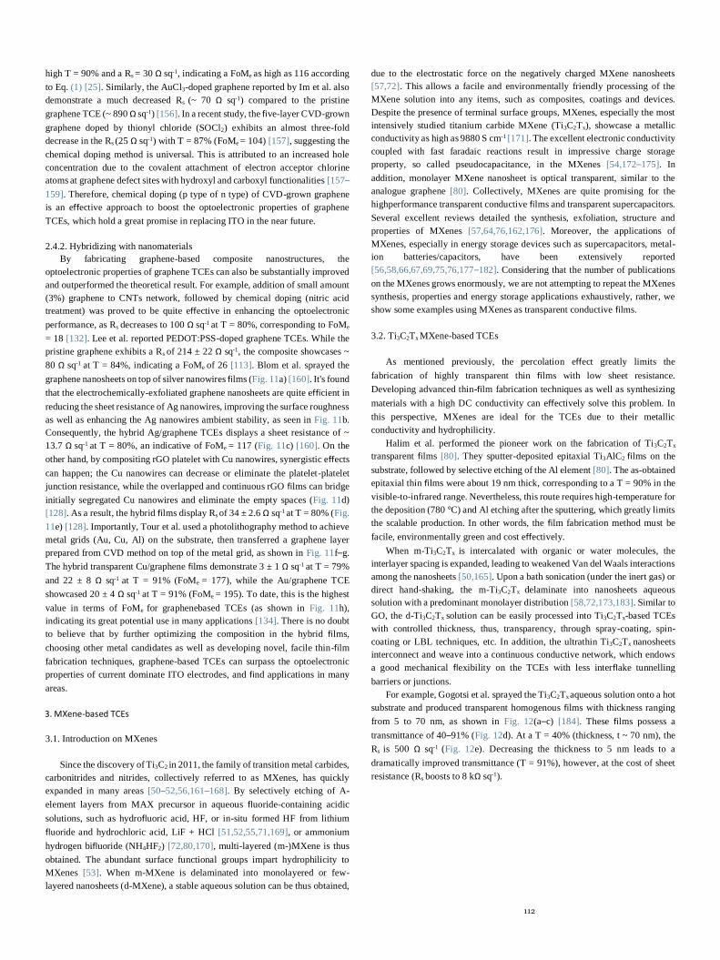
For example, Gogotsi et al. sprayed the Ti3C2Tx aqueous solution onto a hot
substrate and produced transparent homogenous films with thickness ranging
from 5 to 70 nm, as shown in Fig. 12(a–c) [184]. These films possess a
transmittance of 40–91% (Fig. 12d). At a T = 40% (thickness, t ~ 70 nm), the
Rs is 500 Ω sq-1 (Fig. 12e). Decreasing the thickness to 5 nm leads to a
dramatically improved transmittance (T = 91%), however, at the cost of sheet
resistance (Rs boosts to 8 kΩ sq-1).

113
According to Eq. (1), the FoMe in these spray-coated Ti3C2Tx TCEs is around
0.5–0.7 [184]. Such a low FoMe may due to the loose morphology in the MXene
TCEs [184]. During the spray coating, the droplets are purged by the gas and
sprayed onto the hot substrate, where the solvent (ethanol [184] or water [185])
get quickly evaporated. The as-generated vapour bubbles the nanosheets and
creates plenty of voids/pores that negatively hinder the smooth transport of
charge carriers among the randomly stacked network. Consequently, the DC
conductivity in the sprayed Ti3C2Tx TCEs is much lower. Another possible
reason is that the intrinsic optical conductivity (σop) of Ti3C2Tx is very high.
Nevertheless, the FoMe in these spray-coated Ti3C2Tx TCEs is still comparable
to the exfoliated graphene TCEs (See Section 2.2.3) [41,42]. In another trial of
spray coating of Ti3C2Tx, the resistivity reaches 3.4 × 10⁴ Ω/cm at a T = 86.7%,
leading to a somewhat low FoMe [185].
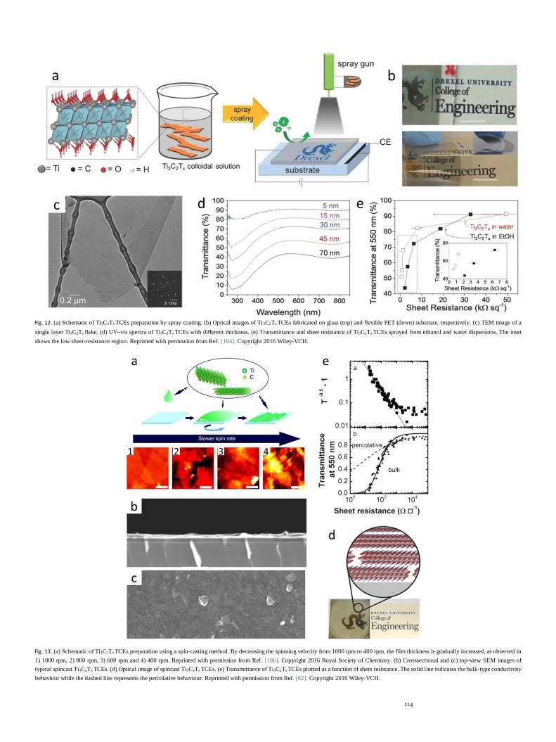
Taylor et al. solution-processed Ti3C2Tx dispersion into TCEs by a spin-
casting method (Fig. 13a) [81]. By controlling the spin velocity, the resultant
Ti3C2Tx film thickness can be efficiently tuned. The metallic conductivity nature
was confirmed in the Ti3C2Tx MXene by field effect transistor measurements,
with an electronic conductivity estimated as high as 3092 S cm-1. Thus, the
Ti3C2Tx films showcased good optoelectronic performances, such as a Rs of 437
Ω sq-1 at the T of 77% [81]. This corresponds to a FoMe of 3.1, a value that is
much higher than the spray-coated Ti3C2Tx TCEs [184]. By vacuum-annealing
the wet MXene films at 175 °C, the trapped water molecules and other
intercalated or adsorbed species can be removed, as a result, the Rs dramatically
reduced from 630 to 191 Ω sq-1 [186]. On the other hand, in the report by
Barsoum et al., the Ti3C2Tx TCEs displayed an electronic conductivity up to
6500 S cm-1 while simultaneously transmitting > 97% of visible light per-
nanometer thickness [82]. Therefore, a layer of nanosheet (~ 1.2 nm in
thickness) leads to ~ 3% loss in transmittance, which is quite comparable to
graphene nanosheets (~ 2.3% transmittance loss per layer, 0.34 nm).
Importantly, the Ti3C2Tx nanosheets reassembled into an ordered, densely
electrically interconnected geometry (Fig. 13b–d), which endows a bulk
conductivity in the Ti3C2Tx TCEs [82]. Consequently, the best Ti3C2Tx TCEs
showcased a FoMe of 7.3 (Rs = 330 Ω sq-1, T = 86%) while the value obtained
from the fitting of the bulk regime is 5 ± 0.5 (Fig. 13e) [82]. However, clear
percolation regime is observed, as evidenced by the saturation in the T0.5 − 1 vs
Rs plot in Fig. 13e. As discussed in Section 2.3.2, such an issue is undesirable
for the TCEs and should be avoided as much as possible.
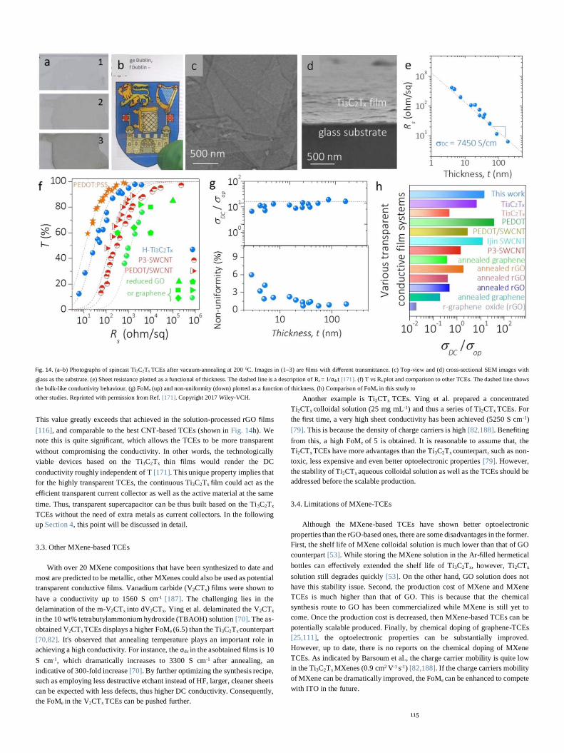
Very recently, we achieved various Ti3C2Tx TCEs with good flake
alignment [171]. By controlling the concentration and spinning velocity, a
range of films with different transmittance were obtained (Fig. 14a–b). These
films showcase an interconnected network without protruding corners of flakes.
A combination of the interconnected network (Fig. 14c–d) and much decreased
boundaries in the micrometer size flakes without water molecules trapped in
between, result in very high DC conductivity up to 9880 S cm-1 (T = 29%, t =
88 nm)
[171].
Interestingly, the Rs of the Ti3C2Tx TCEs scales almost inversely of t, as
shown in Fig. 14e. Such a behaviour is typical seen in the bulk-like materials.
In other words, no apparent percolation problems are encountered in the
Ti3C2Tx TCEs. This is further verified by the T vs Rs plot in Fig. 14f, as the
measured (T, Rs) data are roughly on the curve without apparent deviation. In
addition, the FoMe values are almost constant in a range of thickness (or T, Fig.
14g). The highest FoMe achieved is 19, similar to the one fitted in Fig. 14f
(FoMe = 16).
Fig. 11. (a) Schematic preparation and (b) Top-view SEM image of Ag nanowire/graphene TCE. The hybrid TCEs were prepared by spray-coating of Ag nanowires and graphene nanosheets in sequence.
(c) Optoelectronic properties of various Ag nanowires/graphene films. Reprinted with permission from Ref. [160]. Copyright 2018 Wiley-VCH. (d) SEM image and (e) optoelectronic properties of Cu
nanowires/graphene TCEs. The Cu nanowires were sprayed first, followed by transferring the spin-casted GO films (which were reduced by hydrazine and annealed) onto the pre-deposited Cu films
with the aid of PMMA. Reprinted with permission from Ref. [128]. Copyright 2013 American Chemical Society. (f–g) Optical images of metal grids/graphene TCEs. The metal grids were
photolithographed, followed by transferring the CVD-grown graphene on top of them with the aid of PMMA. (h) Comparison of optoelectronic properties of metal grids/graphene TCEs with literature.
Reprinted with permission from Ref. [134]. Copyright 2011 American Chemical Society.
114
Fig. 12. (a) Schematic of Ti3C2Tx TCEs preparation by spray coating. (b) Optical images of Ti3C2Tx TCEs fabricated on glass (top) and flexible PET (down) substrate, respectively. (c) TEM image of a
single layer Ti3C2Tx flake. (d) UV–vis spectra of Ti3C2Tx TCEs with different thickness. (e) Transmittance and sheet resistance of Ti3C2Tx TCEs sprayed from ethanol and water dispersions. The inset
shows the low sheet-resistance region. Reprinted with permission from Ref. [184]. Copyright 2016 Wiley-VCH.
Fig. 13. (a) Schematic of Ti3C2Tx TCEs preparation using a spin-casting method. By decreasing the spinning velocity from 1000 rpm to 400 rpm, the film thickness is gradually increased, as observed in
1) 1000 rpm, 2) 800 rpm, 3) 600 rpm and 4) 400 rpm. Reprinted with permission from Ref. [186]. Copyright 2016 Royal Society of Chemistry. (b) Crosssectional and (c) top-view SEM images of
typical spincast Ti3C2Tx TCEs. (d) Optical image of spincast Ti3C2Tx TCEs. (e) Transmittance of Ti3C2Tx TCEs plotted as a function of sheet resistance. The solid line indicates the bulk-type conductivity
behaviour while the dashed line represents the percolative behaviour. Reprinted with permission from Ref. [82]. Copyright 2016 Wiley-VCH.
115
Fig. 14. (a–b) Photographs of spincast Ti3C2Tx TCEs after vacuum-annealing at 200 °C. Images in (1–3) are films with different transmittance. (c) Top-view and (d) cross-sectional SEM images with
glass as the substrate. (e) Sheet resistance plotted as a functional of thickness. The dashed line is a description of Rs = 1/σdct [171]. (f) T vs Rs plot and comparison to other TCEs. The dashed line shows
the bulk-like conductivity behaviour. (g) FoMe (up) and non-uniformity (down) plotted as a function of thickness. (h) Comparison of FoMe in this study to
other studies. Reprinted with permission from Ref. [171]. Copyright 2017 Wiley-VCH.
This value greatly exceeds that achieved in the solution-processed rGO films
[116], and comparable to the best CNT-based TCEs (shown in Fig. 14h). We
note this is quite significant, which allows the TCEs to be more transparent
without compromising the conductivity. In other words, the technologically
viable devices based on the Ti3C2Tx thin films would render the DC
conductivity roughly independent of T [171]. This unique property implies that
for the highly transparent TCEs, the continuous Ti3C2Tx film could act as the
efficient transparent current collector as well as the active material at the same
time. Thus, transparent supercapacitor can be thus built based on the Ti3C2Tx
TCEs without the need of extra metals as current collectors. In the following
up Section 4, this point will be discussed in detail.
3.3. Other MXene-based TCEs
With over 20 MXene compositions that have been synthesized to date and
most are predicted to be metallic, other MXenes could also be used as potential
transparent conductive films. Vanadium carbide (V2CTx) films were shown to
have a conductivity up to 1560 S cm-1 [187]. The challenging lies in the
delamination of the m-V2CTx into dV2CTx. Ying et al. delaminated the V2CTx
in the 10 wt% tetrabutylammonium hydroxide (TBAOH) solution [70]. The as-
obtained V2CTx TCEs displays a higher FoMe (6.5) than the Ti3C2Tx counterpart
[70,82]. It's observed that annealing temperature plays an important role in
achieving a high conductivity. For instance, the σdc in the asobtained films is 10
S cm-1, which dramatically increases to 3300 S cm-1 after annealing, an
indicative of 300-fold increase [70]. By further optimizing the synthesis recipe,
such as employing less destructive etchant instead of HF, larger, cleaner sheets
can be expected with less defects, thus higher DC conductivity. Consequently,
the FoMe in the V2CTx TCEs can be pushed further.
Another example is Ti2CTx TCEs. Ying et al. prepared a concentrated
Ti2CTx colloidal solution (25 mg mL-1) and thus a series of Ti2CTx TCEs. For
the first time, a very high sheet conductivity has been achieved (5250 S cm-1)
[79]. This is because the density of charge carriers is high [82,188]. Benefiting
from this, a high FoMe of 5 is obtained. It is reasonable to assume that, the
Ti2CTx TCEs have more advantages than the Ti3C2Tx counterpart, such as non-
toxic, less expensive and even better optoelectronic properties [79]. However,
the stability of Ti2CTx aqueous colloidal solution as well as the TCEs should be
addressed before the scalable production.
3.4. Limitations of MXene-TCEs
Although the MXene-based TCEs have shown better optoelectronic
properties than the rGO-based ones, there are some disadvantages in the former.
First, the shelf life of MXene colloidal solution is much lower than that of GO
counterpart [53]. While storing the MXene solution in the Ar-filled hermetical
bottles can effectively extended the shelf life of Ti3C2Tx, however, Ti2CTx
solution still degrades quickly [53]. On the other hand, GO solution does not
have this stability issue. Second, the production cost of MXene and MXene
TCEs is much higher than that of GO. This is because that the chemical
synthesis route to GO has been commercialized while MXene is still yet to
come. Once the production cost is decreased, then MXene-based TCEs can be
potentially scalable produced. Finally, by chemical doping of graphene-TCEs
[25,111], the optoelectronic properties can be substantially improved.
However, up to date, there is no reports on the chemical doping of MXene
TCEs. As indicated by Barsoum et al., the charge carrier mobility is quite low
in the Ti3C2Tx MXenes (0.9 cm2 V-1 s-1) [82,188]. If the charge carriers mobility
of MXene can be dramatically improved, the FoMe can be enhanced to compete
with ITO in the future.

116
4. Transparent supercapacitors
4.1. Introduction on the transparent supercapacitors
As mentioned previously, one of the most important trends in the portable
electronics is to develop flexible, touchable, and transparent products [1,6].
This require all the crucial components, including energy storage device, to be
resilient and transparent as well [15,23,171]. Supercapacitors, also known as
electrochemical capacitors, are devices that can be charged-discharged in
seconds, and deliver a high power density with a long lifetime, in contrast to
the undesirable charging-discharging rate and lifetime in Li-ion batteries
[23,54,71,141,164,167,169,171,173,174,181,189–209]. However, the energy
density for the supercapacitors (SC) is one order of magnitude lower than that
of Li-ion batteries [54,141,169,193,201–204,208]. For the potential
incorporation of SC into the transparent portable electronics, both the energy
density and power density need to be improved considerably. For any SC, the
performance metrics are the stored energy (E) and power output (P):
E =2
(5)
P =
4RESR (6)
In the perspective of materials, the electrode capacitance (C) should be
maximized while the equivalent series resistance (RESR) be minimized. For the
device, the operated voltage window (V) is limited by the aqueous electrolyte
(1.2 V) and can be overcome by building the asymmetric configuration
[23,210]. The key limitation lies in the development of high performance TCEs.
Unlike the conventional TCEs which only conduct the electrons, TCEs for the
transparent SCs need to possess a good charge-storage property. This is quite
challenging, as approaching high T, percolation problems are usually
encountered in the TCEs, leading to quite high RESR, low C and thus undesirable
E and P. Said otherwise, high-performance transparent SC requires the TCEs
to possess two high figure of merits, electrical FoMe and capacitive FoMc, at the
same time. While the former indicates the capability to conduct electrons at
high transparency, as discussed previously [42,132], the latter (defined as the
ratio of volumetric capacitance to optical conductivity, Cv/σop) is an indicative
of ability to store electrochemical energy in the transparent region [23,171].
Typically, a high FoMe implies good rate handling properties (thus power
output, P) in the transparent SC, while a high FoMc suggests good energy
storage properties (E).
In this regard, the mainstream for developing transparent SC is focused on
the quest of active materials. While metal grids (such as Ag, Cu, etc.) showcase
very high FoMe [16–18,128,160], they are not capacitive materials and thus
cannot be used in transparent SC alone. On the other hand, CNTs, transition
metal oxides and conductive polymers not only demonstrate a great potential
for the TCEs with FoMe as high as 39 in the case of PEDOT:PSS [15], but also
find applications in the transparent SC [15,39,40,211–222]. For example,
Higgins and Coleman spray-coated the PEDOT:PSS solution onto PET
substrates, the as-obtained TCE was used as both the transparent current
collector and active material for transparent SC, which demonstrated a high rate
capability and a high areal capacitance (up to 1.9 mF cm-2 for the T = 70% film)
without apparent percolation problems [15]. On the other hand, Wang et al.
deposited PEDOT:PSS and MnO2 onto the Ni mesh TCEs via spin-casting
strategy and electrodeposition methods, respectively [12,223]. By using the Ni
mesh network as the transparent current collector, a high FoMe as high as 104 is
thus obtained. The PEDOT:PSS or MnO2 layer contribute to the capacitive
charge storage. Consequently, the capacitive behaviour up to 100 V s-1 was
achieved [12,223]. CNTs or carbon-based materials used as transparent, solid-
state SC electrode were also reported [211,219,224,225]. For instances, Ajayan
et al. reported nano-engineered carbon films from porous template and used as
transparent SC electrode, demonstrating both long-term cycling and flexibility
in the device [224]. By vacuum-filtration of SWCNT dispersion followed by a
stamping method, Unalan et al. made SWCNT-based transparent SC which
showcased good charge-storage properties [225]. It is important to emphasize
that, unlike traditional SC electrodes, the gravimetric capacitance, CM, is of
little relevance when evaluating the chargestorage performance of transparent
SCs. This is because the mass of the TCEs is insignificant compared with that
of the substrates. Furthermore, to measure the mass of TCEs exactly is quite
challenging [15]. As an alternative, all the evaluation metrics of transparent SC
should be based on the geometrical area of the device. For example, areal
capacitance (C/A, mF cm-2), energy density (E/A, MW h cm-2) and power
density (P/A, W cm-2), etc. are frequently used for the electrochemical
characterizations of transparent SCs.
Unlike the 3D carbons which exhibit winded ion diffusion paths, 2D
nanosheets can directly expose the active sites to the electrolyte. The shortened
ion diffusion paths coupled with excellent electronic conductivity in the 2D
nanosheets-based TCEs should render good chargestorage properties in the
transparent SCs. In this regard, we focus on the 2D nanosheets, specifically,
graphene and MXene TCEs, for transparent supercapacitors application,
despite these TCEs also demonstrate a great potential in other applications, such
as touch panel, displays, solar cell, to name just a few (Fig. 1) [1,2,6].
4.2. Graphene-based transparent supercapacitors
Lee et al. deposited graphene quantum dots (QDs) onto CVD-grown
graphene interdigitated fingers using an electrophoretic method [49]. Using the
underneath CVD-graphene TCE as the current collector and graphene QDs as
the active materials, the device demonstrates excellent rate response (relaxation
time of 8.5 ms) and high transparency (93%) as well as long-term cycling (~
100% after 10,000 cycles) [49]. By transferring the CVD-grown graphene films
onto PDMS substrate using the methods that described in Section 2.2.1,
transparent SC can be immediately built through sandwiching the graphene/
PDMS electrode with gel electrolyte (such as polyvinyl alcohol, PVA, and
H3PO4) [46,47,226], the latter works as both the separator and solid-state
electrolyte. This process is demonstrated in Fig. 15a. In a typical run, Dai et al.
reported a graphene-based transparent SC, which demonstrates a T of 86% with
good rate response and capacitive behaviour (Fig. 15b–c) [226]. The C/A of the
transparent SC reaches 4.2 µF cm-2 [226]. By introducing the wrinkles on the
CVD-grown graphene TCEs, transparent, flexible and stretchable SCs can be
fabricated as a result. For instances, Dai et al. produced the wrinkled CVD-
grown graphene films using a wrinkled Cu foil (extruded by tweezers) [46].
Benefiting from the unique morphology (Fig. 15d), the resultant SC displays a
good stretchability (up to 40% strain) in the course of hundreds of stretching
cycles without obvious performance change. In addition, the C/A of the
transparent SC reaches 5.8 µF cm-2 at a T of 57% and the capacitance keeps
almost constant upon stretching, as shown in Fig. 15e [46]. On the other hand,
by using a prestraining-then-buckling method, Chou et al. were able to fabricate
stretchable transparent SC based on the few-layer CVD-grown graphene
assisted by the PDMS lamination [227]. As indicated in Fig. 15f, due to the
mismatch of the elastic modulus between graphene film and PDMS substrate,
a buckled morphology of graphene films was obtained. Upon stretching, the
electrochemical performance of the transparent SC is even larger than that of
the planar state, i.e., 5.33 µF cm-2 in the 40% stretched device vs 4.27 µF cm-2
in the planar device at the same T of 73% (Fig. 15g–h) [227].
2
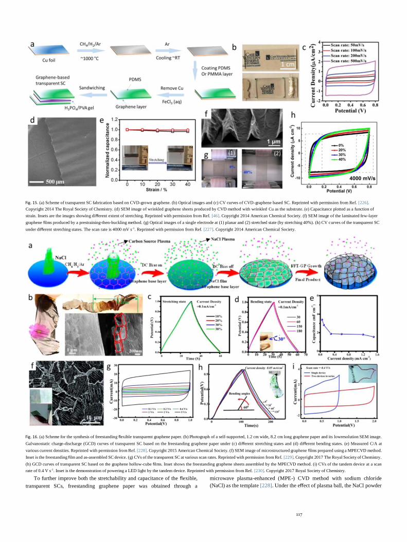
117
Fig. 15. (a) Scheme of transparent SC fabrication based on CVD-grown graphene. (b) Optical images and (c) CV curves of CVD-graphene based SC. Reprinted with permission from Ref. [226].
Copyright 2014 The Royal Society of Chemistry. (d) SEM image of wrinkled graphene sheets produced by CVD method with wrinkled Cu as the substrate. (e) Capacitance plotted as a function of
strain. Insets are the images showing different extent of stretching. Reprinted with permission from Ref. [46]. Copyright 2014 American Chemical Society. (f) SEM image of the laminated few-layer
graphene films produced by a prestraining-then-buckling method. (g) Optical images of a single electrode at (1) planar and (2) stretched state (by stretching 40%). (h) CV curves of the transparent SC
under different stretching states. The scan rate is 4000 mV s-1. Reprinted with permission from Ref. [227]. Copyright 2014 American Chemical Society.
Fig. 16. (a) Scheme for the synthesis of freestanding flexible transparent graphene paper. (b) Photograph of a self-supported, 1.2 cm wide, 8.2 cm long graphene paper and its lowresolution SEM image.
Galvanostatic charge-discharge (GCD) curves of transparent SC based on the freestanding graphene paper under (c) different stretching states and (d) different bending states. (e) Measured C/A at
various current densities. Reprinted with permission from Ref. [228]. Copyright 2015 American Chemical Society. (f) SEM image of microstructured graphene films prepared using a MPECVD method.
Inset is the freestanding film and as-assembled SC device. (g) CVs of the transparent SC at various scan rates. Reprinted with permission from Ref. [229]. Copyright 2017 The Royal Society of Chemistry.
(h) GCD curves of transparent SC based on the graphene hollow-cube films. Inset shows the freestanding graphene sheets assembled by the MPECVD method. (i) CVs of the tandem device at a scan
rate of 0.4 V s-1. Inset is the demonstration of powering a LED light by the tandem device. Reprinted with permission from Ref. [230]. Copyright 2017 Royal Society of Chemistry.
To further improve both the stretchability and capacitance of the flexible,
transparent SCs, freestanding graphene paper was obtained through a
microwave plasma-enhanced (MPE-) CVD method with sodium chloride
(NaCl) as the template [228]. Under the effect of plasma ball, the NaCl powder
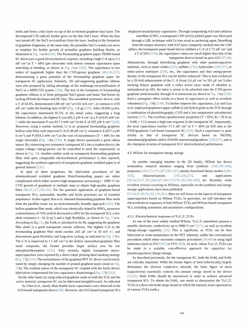
118
melts and forms a thin layer on top of the as-formed graphene base layer. The
decomposed C/H radicals further grow on the thin NaCl layer. When the bias
was turned off, the NaCl recrystallizes from the layer, leading to the formation
of graphene fragments, at the same time, the prismlike NaCl crystals can serve
as template for further growth of prismlike graphene building blocks, as
illustrated in Fig. 16a–b [228]. The freestanding graphene paper/ PDMS-based
SC showcases a good electrochemical response, including a high C/A up to 3.1
mF cm-2 at T = 68% (per electrode) with almost constant capacitance upon
stretching or bending, as shown in Fig. 16ce [228]. The capacitance is two
orders of magnitude higher than the CVD-grown graphene [46,226,227],
demonstrating a great potential of the freestanding graphene paper for
transparent SC application. Similarly, 3D self-supporting graphene ribbons
were also prepared by taking advantage of the multistage-recrystallization of
NaCl in a MPECVD system [229]. The key to the formation of freestanding
graphene ribbons is to form polygonal NaCl-grains and linear NaCltwins by
turning off both the heater and DC bias. The assembled symmetric device, with
a T of 50.6%, demonstrated 4.88 mF cm-2 at 0.02 mA cm-2, in contrast to 4.95
mF cm-2 under the bending state of 60° (Fig. 16f–g) [229]. After 20,000 cycles,
the capacitance maintained 95.5% of the initial value, suggesting a long
lifetime. In addition, the highest E was 605.2 µW h cm-3 at a P of 8.93 mW cm-
3, while the maximum P was 817.3 mW cm-3 at the E of 295 µW h cm-3 [229].
Moreover, using a similar method, Li et al. prepared freestanding graphene
hollow-cube films with improved C/A (5.48 mF cm-2), volumetric E (657.2 µW
h cm-3) and P (954.3 mW cm-3) at the cost of transmittance (T = 44% for the
single electrode) (Fig. 16h) [230]. A single device possessed a good robust
nature. By connecting two symmetric transparent SCs into a tandem device, the
output voltage/ energy/power can be controlled to meet the requirement, as
shown in Fig. 16i. Another similar work on transparent freestanding graphene
films with quite comparable electrochemical performance is also reported,
suggesting the synthesis approach of transparent graphene wrinkled paper is of
general interest [231].
In spite of these progresses, the fabrication procedures of the
aforementioned wrinkled graphene films/freestanding papers are rather
complicated which either involve high temperature processing (~ 1000 °C for
CVD growth of graphene) or multiple steps to obtain high-quality graphene
films [46,47,227,228,230]. For the potential application of graphene-based
transparent SCs, sustainable, feasible and facile processes are of essential
importance. In this regard, Hsu et al. obtained freestanding graphene fiber mesh
from the parafilm waste via an environmentally friendly approach [232]. The
hollow graphene fiber mesh, which was chemically-doped by HNO3, possesses
a transmittance of 76% (which decreased to 69% for the transparent SC), a low
sheet resistance (~ 32 Ω sq-1) and a high flexibility, as shown in Fig. 17a–e.
According to Eq. (1), the FoMe is calculated to be 40, suggesting the graphene
fiber alone is a good transparent current collector. The highest C/A in the
freestanding graphene fiber mesh reaches 245 µF cm-2 at 50 mV s-1, and
demonstrate good flexibility and long-term cycling, as indicated in Fig. 17f–i.
The C/A is improved to 1.1 mF cm-2 in the hollow nanocarbon/graphene fiber
mesh composite, the former provides larger surface area for ion
adsorption/desorption [232]. Very recently, highly transparent micro-
supercapacitors were reported by a direct inkjet printing-hard masking strategy
(Fig. 17j) [233]. The transmittance of the graphene/PET SC device can be easily
tuned by simply changing the number of printed graphene layers (inset in Fig.
17k). The resilient nature of the transparent SC coupled with the facile device
fabrication compensated the low-capacitance disadvantage (Fig. 17l) [233].
On the other hand, by using reduced graphene oxide as both the TCE and the
active material, transparent SC can be fabricated straightforward. As indicated
by Chen et al., nearly ideal double-layer capacitance were observed in the
rGO-based transparent device [48]. However, the rGO-based transparent SCs
displayed unsatisfactory capacitance. Through compositing rGO and cellulose
nanofiber (CNF), a transparent CNF-(rGO)n hybrid paper was fabricated
through a LBL technique with Cu ions acted as anchoring agent. Benefiting
from the unique structure, with rGO layer compactly stacked onto the CNF
pillars, the transparent paper-based device exhibits a C/A of 1.73 mF cm-2 and
a T of 56% [234], the capacitance values are much higher than that of the
transparent devices based on pure rGO [47,48].
Alternatively, through hybridizing graphene with other pseudocapacitive
materials, such as metal oxides [220], sulfides [235], hydroxides [236,237], or
redox-active interlayer [238], etc., the capacitance and thus energy/power
density of the transparent SCs can be further enhanced. This is best evidenced
by a 20-fold enhancement of the C/ A (from 5.6 µF cm-2 to 101 µF cm-2) after
stacking bilayer graphene with a redox active layer made of ultrathin p-
aminophenol (p-AP), the latter is prone to be adsorbed onto the CVD-grown
graphene predominantly through π–π interaction (as shown in Fig. 18a) [238].
Such a synergistic effect results in a boost of capacitance as well as excellent
robustness (Fig. 18b) [238]. To further improve the capacitance, Liu and Guo
et al. employed graphene/copper sulfide (CuS) hybrid grids as the TCE through
a combination of photolithography, CVD and a low temperature solvothermal
reaction [235]. The excellent optoelectronic properties (T = 85%, Rs = 20 Ω sq-
1, FoMe = 111) ensure a high-rate response in the transparent SC. Importantly,
the areal capacitance reaches 17.3 mF cm-2 at T = 40% (at 620 nm) in the
PANi/graphene/ CuS-based transparent SC [235]. Such a capacitance is quite
similar as that of transparent SC devices based on Ni(OH)2
nanosheets@graphene and/or FeOOH nanowires@graphene [236,237], and is
the champion in terms of transparent SCs’ electrochemical performance.
4.3. MXene for transparent energy storage
As another emerging member in the 2D family, MXene has drawn
tremendous research attention ranging from synthesis [168,239–244],
properties [165,172,175,187,245–247], density functional theory studies [248–
255], characterizations [165,256,257], and applications
[50,54,55,71,163,164,167,169,173,179–181,258–260], etc. Recently, some
excellent reviews covering on MXenes, especially on the synthesis and energy
storage applications, have been published
[57,64,67,69,76,162,176,261]. Here we will focus on the aspects of transparent
supercapacitors based on MXene TCEs. In particular, we will introduce the
electrochemical responses of both MXene TCEs and MXene-based transparent
SCs, including symmetric and asymmetric configurations.
4.3.1. Electrochemical responses of Ti3C2Tx TCEs
As one of the most widely studied MXene, Ti3C2Tx nanosheets possess a
metallic electronic conductivity up to 9880 S cm-1 [171], as well as excellent
charge-storage capability [55]. This is significant, as TCEs can be thus
fabricated at room-temperature on the PET substrate, unlike the conventional
procedures which either encounter complex procedures [39,40] or using rigid
substrates (such as ITO [262] or FTO [40]). As such, robust Ti3C2Tx TCEs can
be made in a scalable, cost-effective approach for capacitive (or
pseudocapacitive) charge storage.
As described previously, for the transparent SC, both the FoMe and FoMc
are critically important. While the former figure of merit (electrically) largely
determines the electron conductive network, the latter figure of merit
(capacitively) essentially controls the amount energy stored in the device
[15,23]. Both FoMs should be maximized in order to achieve advanced
transparent SCs. To obtain the FoMc, one needs to characterize the Ti3C2Tx
TCEs in a three-electrode setup, based on which the intrinsic areal capacitances
of various TCEs (with a

119
Fig. 17. (a) Effect of acid pretreatment time on the sheet resistance of the few-layer graphene/Ni meshes and hollow few-layer graphene fiber mesh (HFGM). (b–e) SEM images of graphene hollow fiber
mesh at different magnifications. (f) CV curves, (g) GCE curves and (h) areal capacitances of transparent, symmetric SC bending at different states. (i) Long-term cycling of the transparent SC devices
tested at bent and flat states. Insets are the typical GCD curves at the 1st and 10,000th cycle of flat and bent devices, respectively. Reprinted with permission from Ref. [232]. Copyright 2017 American
Chemical Society. (j) Scheme of graphene-based transparent SC fabrication using an inkjet printing-hard masking strategy. (k) The as-printed graphene transparent SC with PET as substrate, showing
a highly flexible property. Inset is the optical images of as-printed graphene films with different number of layers ranging from 5 L (left) to 20 L (right). (l) C/A of graphene-based transparent SCs with
different number of printed layers. Reprinted with permission from Ref. [233]. Copyright 2017 Royal Society of Chemistry.
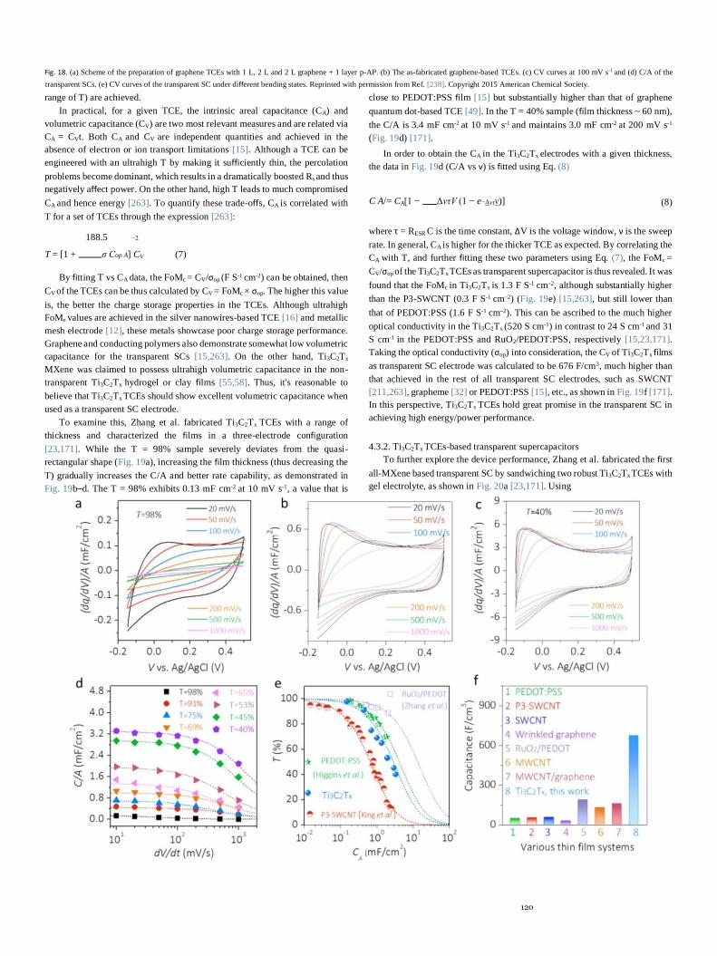
120
Fig. 18. (a) Scheme of the preparation of graphene TCEs with 1 L, 2 L and 2 L graphene + 1 layer p-AP. (b) The as-fabricated graphene-based TCEs. (c) CV curves at 100 mV s-1 and (d) C/A of the
transparent SCs. (e) CV curves of the transparent SC under different bending states. Reprinted with permission from Ref. [238]. Copyright 2015 American Chemical Society.
range of T) are achieved.
In practical, for a given TCE, the intrinsic areal capacitance (CA) and
volumetric capacitance (CV) are two most relevant measures and are related via
CA = CVt. Both CA and CV are independent quantities and achieved in the
absence of electron or ion transport limitations [15]. Although a TCE can be
engineered with an ultrahigh T by making it sufficiently thin, the percolation
problems become dominant, which results in a dramatically boosted Rs and thus
negatively affect power. On the other hand, high T leads to much compromised
CA and hence energy [263]. To quantify these trade-offs, CA is correlated with
T for a set of TCEs through the expression [263]:
188.5 −2
T = [1 + σ Cop A] CV (7)
By fitting T vs CA data, the FoMc = CV/σop (F S-1 cm-2) can be obtained, then
CV of the TCEs can be thus calculated by CV = FoMc × σop. The higher this value
is, the better the charge storage properties in the TCEs. Although ultrahigh
FoMe values are achieved in the silver nanowires-based TCE [16] and metallic
mesh electrode [12], these metals showcase poor charge storage performance.
Graphene and conducting polymers also demonstrate somewhat low volumetric
capacitance for the transparent SCs [15,263]. On the other hand, Ti3C2Tx
MXene was claimed to possess ultrahigh volumetric capacitance in the non-
transparent Ti3C2Tx hydrogel or clay films [55,58]. Thus, it's reasonable to
believe that Ti3C2Tx TCEs should show excellent volumetric capacitance when
used as a transparent SC electrode.
To examine this, Zhang et al. fabricated Ti3C2Tx TCEs with a range of
thickness and characterized the films in a three-electrode configuration
[23,171]. While the T = 98% sample severely deviates from the quasi-
rectangular shape (Fig. 19a), increasing the film thickness (thus decreasing the
T) gradually increases the C/A and better rate capability, as demonstrated in
Fig. 19b–d. The T = 98% exhibits 0.13 mF cm-2 at 10 mV s-1, a value that is
close to PEDOT:PSS film [15] but substantially higher than that of graphene
quantum dot-based TCE [49]. In the T = 40% sample (film thickness ~ 60 nm),
the C/A is 3.4 mF cm-2 at 10 mV s-1 and maintains 3.0 mF cm-2 at 200 mV s-1
(Fig. 19d) [171].
In order to obtain the CA in the Ti3C2Tx electrodes with a given thickness,
the data in Fig. 19d (C/A vs ν) is fitted using Eq. (8)
C A/= CA[1 − ΔντV (1 − e−ΔντV)] (8)
where τ = RESR C is the time constant, ΔV is the voltage window, ν is the sweep
rate. In general, CA is higher for the thicker TCE as expected. By correlating the
CA with T, and further fitting these two parameters using Eq. (7), the FoMc =
CV/σop of the Ti3C2Tx TCEs as transparent supercapacitor is thus revealed. It was
found that the FoMc in Ti3C2Tx is 1.3 F S-1 cm−2, although substantially higher
than the P3-SWCNT (0.3 F S-1 cm−2) (Fig. 19e) [15,263], but still lower than
that of PEDOT:PSS (1.6 F S-1 cm−2). This can be ascribed to the much higher
optical conductivity in the Ti3C2Tx (520 S cm-1) in contrast to 24 S cm-1 and 31
S cm-1 in the PEDOT:PSS and RuO2/PEDOT:PSS, respectively [15,23,171].
Taking the optical conductivity (σop) into consideration, the CV of Ti3C2Tx films
as transparent SC electrode was calculated to be 676 F/cm3, much higher than
that achieved in the rest of all transparent SC electrodes, such as SWCNT
[211,263], grapheme [32] or PEDOT:PSS [15], etc., as shown in Fig. 19f [171].
In this perspective, Ti3C2Tx TCEs hold great promise in the transparent SC in
achieving high energy/power performance.
4.3.2. Ti3C2Tx TCEs-based transparent supercapacitors
To further explore the device performance, Zhang et al. fabricated the first
all-MXene based transparent SC by sandwiching two robust Ti3C2Tx TCEs with
gel electrolyte, as shown in Fig. 20a [23,171]. Using
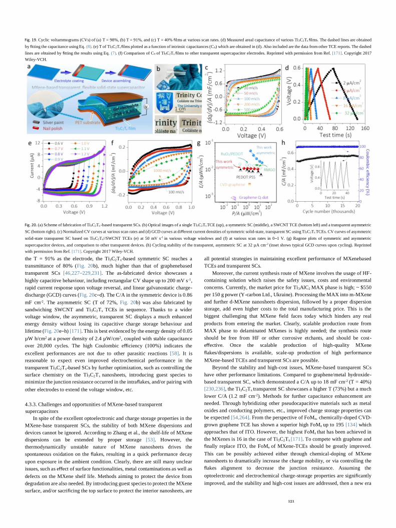
121
Fig. 19. Cyclic voltammograms (CVs) of (a) T = 98%, (b) T = 91%, and (c) T = 40% films at various scan rates. (d) Measured areal capacitance of various Ti3C2Tx films. The dashed lines are obtained
by fitting the capacitance using Eq. (8). (e) T of Ti3C2Tx films plotted as a function of intrinsic capacitances (CA) which are obtained in (d). Also included are the data from other TCE reports. The dashed
lines are obtained by fitting the results using Eq. (7). (f) Comparison of CV of Ti3C2Tx films to other transparent supercapacitor electrodes. Reprinted with permission from Ref. [171]. Copyright 2017
Wiley-VCH.
Fig. 20. (a) Scheme of fabrication of Ti3C2Tx -based transparent SCs. (b) Optical images of a single Ti3C2Tx TCE (up), a symmetric SC (middle), a SWCNT TCE (bottom left) and a transparent asymmetric
SC (bottom right). (c) Normalized CV curves at various scan rates and (d) GCD curves at different current densities of symmetric solid-state, transparent SC using Ti3C2Tx TCEs. CV curves of asymmetric
solid-state transparent SC based on Ti3C2Tx//SWCNT TCEs (e) at 50 mV s-1 in various voltage windows and (f) at various scan rates in 0–1 V. (g) Ragone plots of symmetric and asymmetric
supercapacitor devices, and comparison to other transparent devices. (h) Cycling stability of the transparent, asymmetric SC at 32 µA cm−2 (inset shows typical GCD curves upon cycling). Reprinted
with permission from Ref. [171]. Copyright 2017 Wiley-VCH.
the T = 91% as the electrode, the Ti3C2Tx-based symmetric SC reaches a
transmittance of 80% (Fig. 20b), much higher than that of graphenebased
transparent SCs [46,227–229,231]. The as-fabricated device showcases a
highly capacitive behaviour, including rectangular CV shape up to 200 mV s-1,
rapid current response upon voltage reversal, and linear galvanostatic charge-
discharge (GCD) curves (Fig. 20c–d). The C/A in the symmetric device is 0.86
mF cm-2. The asymmetric SC (T of 72%, Fig. 20b) was also fabricated by
sandwiching SWCNT and Ti3C2Tx TCEs in sequence. Thanks to a wider
voltage window, the asymmetric, transparent SC displays a much enhanced
energy density without losing its capacitive charge storage behaviour and
lifetime (Fig. 20e–h) [171]. This is best evidenced by the energy density of 0.05
µW h/cm2 at a power density of 2.4 µW/cm2, coupled with stable capacitance
over 20,000 cycles. The high Coulombic efficiency (100%) indicates the
excellent performances are not due to other parasitic reactions [58]. It is
reasonable to expect even improved electrochemical performance in the
transparent Ti3C2Tx-based SCs by further optimization, such as controlling the
surface chemistry on the Ti3C2Tx nanosheets, introducing guest species to
minimize the junction resistance occurred in the intraflakes, and/or pairing with
other electrodes to extend the voltage window, etc.
4.3.3. Challenges and opportunities of MXene-based transparent
supercapacitors
In spite of the excellent optoelectronic and charge storage properties in the
MXene-base transparent SCs, the stability of both MXene dispersions and
devices cannot be ignored. According to Zhang et al., the shelf-life of MXene
dispersions can be extended by proper storage [53]. However, the
thermodynamically unstable nature of MXene nanosheets drives the
spontaneous oxidation on the flakes, resulting in a quick performance decay
upon exposure in the ambient condition. Clearly, there are still many unclear
issues, such as effect of surface functionalities, metal contaminations as well as
defects on the MXene shelf life. Methods aiming to protect the device from
degradation are also needed. By introducing guest species to protect the MXene
surface, and/or sacrificing the top surface to protect the interior nanosheets, are
all potential strategies in maintaining excellent performance of MXenebased
TCEs and transparent SCs.
Moreover, the current synthesis route of MXene involves the usage of HF-
containing solution which raises the safety issues, costs and environmental
concerns. Currently, the market price for Ti3AlC2 MAX phase is high; ~ $550
per 150 g power (Y-carbon Ltd., Ukraine). Processing the MAX into m-MXene
and further d-MXene nanosheets dispersion, followed by a proper dispersion
storage, add even higher costs to the total manufacturing price. This is the
biggest challenging that MXene field faces today which hinders any real
products from entering the market. Clearly, scalable production route from
MAX phase to delaminated MXenes is highly needed; the synthesis route
should be free from HF or other corrosive etchants, and should be cost-
effective. Once the scalable production of high-quality MXene
flakes/dispersions is available, scale-up production of high performance
MXene-based TCEs and transparent SCs are possible.
Beyond the stability and high-cost issues, MXene-based transparent SCs
have other performance limitations. Compared to graphene/metal hydroxide-
based transparent SC, which demonstrated a C/A up to 18 mF cm-2 (T = 40%)
[230,236], the Ti3C2Tx transparent SC showcases a higher T (73%) but a much
lower C/A (1.2 mF cm-2). Methods for further capacitance enhancement are
needed. Through hybridizing other pseudocapacitive materials such as metal
oxides and conducting polymers, etc., improved charge storage properties can
be expected [54,264]. From the perspective of FoMe, chemically-doped CVD-
grown graphene TCE has shown a superior high FoMe up to 195 [134] which
approaches that of ITO. However, the highest FoMe that has been achieved in
the MXenes is 16 in the case of Ti3C2Tx [171]. To compete with graphene and
finally replace ITO, the FoMe of MXene-TCEs should be greatly improved.
This can be possibly achieved either through chemical-doping of MXene
nanosheets to dramatically increase the charge mobility, or via controlling the
flakes alignment to decrease the junction resistance. Assuming the
optoelectronic and electrochemical charge-storage properties are significantly
improved, and the stability and high-cost issues are addressed, then a new era

122
of MXenes is coming, which will open numerous opportunities in the cutting-
edge applications.
5. Summary and outlook
Over the past several decades, the industry of portable electronics has been
quickly expanded in our daily life. One of key technologies in these products is
to develop high-performance transparent conductive electrodes (TCEs). Indium
tin oxide (ITO) has dominated the market for a long time, despite its drawbacks
such as brittleness, high-cost and complicated fabrication procedures. Questing
materials to replace ITO for future flexible, wearable, interacted electronics is
of highly urgent. Conductive polymers have been regarded as promising
candidates, however, the poor environmental stability and noticeable colour
limit their applications. One-dimensional carbon nanotube or silver nanowires
have shown excellent optoelectronic properties, including high figure of merit
(FoMe) which serves an important evaluation metrics in the field of TCEs.
However, the surface roughness in these CNT or Ag nanowires-based TCEs are
serious concerns, especially the haze effect in the latter.
Two-dimensional materials, with unique properties in many areas, have
attracted intensive research attention in recent years. Due to the high charge
carrier concentrations and mobility, graphene nanosheets have been regarded
as the most promising candidate for replacing ITO. While reduced-graphene
oxide and liquid-exfoliated graphene dispersions enable a quick fabrication of
TCEs through the solution-processing techniques (including spin-, spray-, dip-
, LBL-coatings, inkjetprinting, hard-masking, etc.), the FoMe in these resultant
TCEs is insignificant with maximum value ~ 1.6 [41]. The chemical vapour
deposition method can precisely control the graphene flake size and number of
layers by choosing different catalytic substrates and changing the CVD
parameters. To date, the CVD-grown graphene has demonstrated the most
promising optoelectronic properties for TCEs, including the benchmark
performance: Rs ~ 30 Ω sq-1 at T = 90% (FoMe = 116) in the 4-layer CVD-
graphene TCE [25], which is quite comparable to the ITO. However, the strict
TCE fabrication procedures coupled with issues such as incomplete etching of
substrates and/or exist of polymer residues during thin film transferring, are the
concerns that must be taken into consideration. Future work on the graphene
TCEs should focus on developing high-quality graphene at lowtemperature and
come up with methods without etching or transferring steps. By combining
graphene freestanding paper with other pseudocapacitive materials and forming
a hybrid, with graphene to transport electrons while redox active materials to
store charge, the graphenebased transparent supercapacitor demonstrate quite
promising electrochemical performance. Further studies should be
concentrated on the facile production of such hybrids with improved
transparency, as the current state-of-the-art transparent supercapacitor
showcase a relative low transmittance ~ 40% [46,227,230]. For potential
incorporation of transparent supercapacitor into transparent electronics, the
higher the critical parameters, including areal/volumetric capacitance,
energy/power density, transmittance, and long-term cycling, etc., the better.
As a new class in the 2D family materials, MXenes possess abundant
surface groups, high electronic conductivities and many other unique
properties, rendering them quite attractive in various applications. Ti3C2Tx is
the most widely studied MXene with an ultrahigh DC conductivity (up to 9880
S cm-1 [171]) and excellent charge-storage properties [55,58]. Although the
optoelectronic properties in the Ti3C2Tx has outperformed that of solution-
processed graphene, however, there is still long distance to reach the ITO
performance. To further push the Ti3C2Tx limit as efficient TCEs, several
directions are proposed. Firstly, increasing the charge carrier mobility of
MXene nanosheets can substantially improve the optoelectronic properties.
This can be realized by chemical-doping the MXene nanosheets or hybridizing
with guest species. Furthermore, understanding the movement of charge
carriers along the tunnelling barriers is also crucial. In addition, optimization of
the MXene synthesis/ composition and understanding the influence of surface
functionalities on the MXene electronic properties should be effective. Finally,
building the MXene nanosheet mesh on the flexible PET can substantially
improves the transmittance of Ti3C2Tx TCEs. This requires a delicate design of
thin film fabrication.
MXene TCEs can be used for high-performance transparent supercapacitor,
with excellent volumetric capacitance, high energy density/ power handing and
long lifetime. While these progresses are exciting, several issues should be paid
with much attention. Stability of the MXene dispersions and devices, large-
scale, environmentally green production of MXenes as well as relatively low
areal capacitance in the prototype cells, are all challenges for MXene-based
transparent supercapacitors. Despite these many challenges, the future of
MXene TCEs is very bright, due to not only the unique properties that MXene
have demonstrated, but also the quite encouraging research results based on the
continuous efforts in this emerging field.
Acknowledgements
The paper was written solely by C.F.Z. This work is supported by European
Research Council (ERC 3D2Dprint).
References
[1] D.S. Hecht, L. Hu, G. Irvin, Adv. Mater. 23 (2011) 1482–1513. [2] Y. Xu, J. Liu, Small 12 (2016) 1400–1419. [3] G. Eda, Y.-Y. Lin, S. Miller, C.-W. Chen, W.-F. Su, M. Chhowalla, Appl. Phys. Lett.
92 (2008) 233305. [4] Y. Yang, S. Jeong, L. Hu, H. Wu, S.W. Lee, Y. Cui, Proc. Natl. Acad. Sci. USA 108
(2011) 13013–13018. [5] D.S. Chang, S. Te Lai, Int. J. Adv. Manuf. Technol. 78 (2015) 753–763. [6] L. Yu, C. Shearer, J. Shapter, Chem. Rev. 116 (2016) 13413–13453.
[7] J. Song, S.A. Kulinich, J. Li, Y. Liu, H. Zeng, Angew. Chem. Int. Ed. 127 (2015) 472–
476. [8] C.-Y. Chen, W.-K. Lee, Y.-J. Chen, C.-Y. Lu, H.Y. Lin, C.-C. Wu, Adv. Mater. 27
(2015) 4883–4888.
[9] M.H. Ahn, E.S. Cho, S.J. Kwon, Vacuum 101 (2014) 221–227. [10] Y. Galagan, A. Mescheloff, S.C. Veenstra, R. Andriessen, E.A. Katz, Phys. Chem.
Chem. Phys. 17 (2015) 3891–3897. [11] C.-C. Kim, H.-H. Lee, K.H. Oh, J.-Y. Sun, Science 353 (2016) 682–687. [12] Y.-H. Liu, J.-L. Xu, S. Shen, X.-L. Cai, L.-S. Chen, S.-D. Wang, J. Mater. Chem. A 5
(2017) 9032–9041. [13] Xuan Wang, A. Linjie Zhi, K. Müllen, Nano Lett. 8 (2008) 323–327. [14] Y. Xia, K. Sun, J. Ouyang, Adv. Mater. 24 (2012) 2436–2440.
[15] T.M. Higgins, J.N. Coleman, ACS Appl. Mater. Interfaces 7 (2015) 16495–16506. [16] S. De, T.M. Higgins, P.E. Lyons, E.M. Doherty, P.N. Nirmalraj, W.J. Blau, J.J.
Boland, J.N. Coleman, ACS Nano 3 (2009) 1767–1774. [17] H. Lu, D. Zhang, X. Ren, J. Liu, W.C.H. Choy, ACS Nano 8 (2014) 19080–19087.
[18] B.Y. Ahn, D.J. Lorang, J.A. Lewis, Nanoscale 3 (2011) 2700–2702. [19] M. Yu, Z. Wang, C. Hou, Z. Wang, C. Liang, C. Zhao, Y. Tong, X. Lu, S. Yang, Adv.
Mater. 29 (2017) 1602868. [20] Y. Zeng, Y. Meng, Z. Lai, X. Zhang, M. Yu, P. Fang, M. Wu, Y. Tong, X. Lu, Adv.
Mater. 29 (2017) 1702698. [21] M. Yu, D. Lin, H. Feng, Y. Zeng, Y. Tong, X. Lu, Angew. Chem. Int. Ed. 56 (2017)
5454–5459. [22] Y. Huang, Y. Zeng, M. Yu, P. Liu, Y. Tong, F. Cheng, X. Lu, Small Methods 2 (2018)
1700230. [23] C. Zhang, T.M. Higgins, S.-H. Park, S.E. O, D. Long, J.N. Coleman, V. Nicolosi, Nano
Energy 28 (2016) 495–505. [24] Y.H. Kim, S.J. Kim, Y.-J. Kim, Y.-S. Shim, S.Y. Kim, B.H. Hong, H.W. Jang, ACS
Nano 9 (2015) 10453–10460. [25] S. Bae, H. Kim, Y. Lee, X. Xu, J.-S. Park, Y. Zheng, J. Balakrishnan, T. Lei, H. Ri Kim,
Y. Il Song, Y.-J. Kim, K.S. Kim, B. Özyilmaz, J.-H. Ahn, B.H. Hong, S. Iijima, Nat.
Nanotechnol. 5 (2010) 574–578.
[26] X. Duan, S. Indrawirawan, H. Sun, S. Wang, Catal. Today 249 (2015) 184–191. [27] H. Ji, L. Zhang, M.T. Pettes, H. Li, S. Chen, L. Shi, R. Piner, R.S. Ruoff, Nano Lett.
12 (2012) 2446–2451. [28] B. Mendoza-Sánchez, B. Rasche, V. Nicolosi, P.S. Grant, Carbon 52 (2013) 337–346. [29] L.T. Le, M.H. Ervin, H. Qiu, B.E. Fuchs, W.Y. Lee, Electrochem. Commun. 13 (2011)
355–358. [30] Y. Wang, Z. Shi, Y. Huang, Y. Ma, C. Wang, M. Chen, Y. Chen, J. Phys. Chem. C 113
(2009) 13103–13107. [31] M. Stoller, S. Park, Y. Zhu, J. An, R. Ruoff, Nano Lett. 8 (2008) 3498–3502. [32] J. Yan,
J. Liu, Z. Fan, T. Wei, L. Zhang, Carbon 50 (2012) 2179–2188.
[33] C.. Rao, K. Gopalakrishnan, U. Maitra, ACS Appl. Mater. Interfaces 7 (2015) 7809–
7832. [34] Q. Liu, J. Chen, Y. Li, G. Shi, ACS Nano 10 (2016) 7901–7906. [35] S. De, J.N. Coleman, MRS Bull. 36 (2011) 774–781.
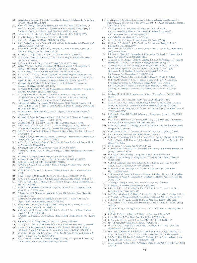
123
[36] B. Ruzicka, L. Degiorgi, R. Gaal, L. Thien-Nga, R. Bacsa, J.-P. Salvetat, L. Forró, Phys.
Rev. B 61 (2000) R2468–R2471. [37] S. De, P.E. Lyons, S. Sorel, E.M. Doherty, P.J. King, W.J. Blau, P.N. Nirmalraj, J.J.
Boland, V. Scardaci, J. Joimel, J.N. Coleman, ACS Nano 3 (2009) 714–720. [38] V.
Scardaci, R. Coull, J.N. Coleman, Appl. Phys. Lett. 97 (2010) 23114. [39] H. Lin, L. Li, J. Ren, Z. Cai, L. Qiu, Z. Yang, H. Peng, Sci. Rep. 3 (2013) 1353. [40] J. Ge, G. Cheng, L. Chen, Nanoscale 3 (2011) 3084–3088. [41] S. De, J.N. Coleman, ACS Nano 4 (2010) 2713–2720. [42] S. De, P.J. King, M. Lotya, A. O’Neill, E.M. Doherty, Y. Hernandez, G.S. Duesberg, J.N.
Coleman, Small 6 (2010) 458–464. [43] K.S. Kim, Y. Zhao, H. Jang, S.Y. Lee, J.M. Kim, K.S. Kim, J.-H. Ahn, P. Kim, J.Y.
Choi, B.H. Hong, Nature 457 (2009) 706–710. [44] X. Yang, C. Cheng, Y. Wang, L. Qiu, D. Li, Science 341 (2013) 534–537. [45] Z.-S. Wu, K. Parvez, S. Li, S. Yang, Z. Liu, S. Liu, X. Feng, K. Müllen, Adv. Mater.
27 (2015) 4054–4061. [46] T. Chen, Y. Xue, A.K. Roy, L. Dai, ACS Nano 8 (2014) 1039–1046. [47] Y. Gao, Y.S. Zhou, W. Xiong, L.J. Jiang, M. Mahjouri-samani, P. Thirugnanam, X.
Huang, M.M. Wang, L. Jiang, Y.F. Lu, APL Mater. 1 (2013) 12101. [48] A. Yu, I. Roes, A. Davies, Z. Chen, Appl. Phys. Lett. 96 (2010) 253105. [49] K. Lee, H. Lee, Y. Shin, Y. Yoon, D. Kim, H. Lee, Nano Energy 26 (2016) 746–754. [50] M.R. Lukatskaya, O. Mashtalir, C.E. Ren, Y. Dall’Agnese, P. Rozier, P.L. Taberna, M.
Naguib, P. Simon, M.W. Barsoum, Y. Gogotsi, Science 341 (2013) 1502–1505. [51] M. Naguib, O. Mashtalir, J. Carle, V. Presser, J. Lu, L. Hultman, Y. Gogotsi, M.
Barsoum, ACS Nano 6 (2012) 1322–1331. [52] M. Naguib, M. Kurtoglu, V. Presser, J. Lu, J. Niu, M. Heon, L. Hultman, Y. Gogotsi, M.
Barsoum, Adv. Mater. 23 (2011) 4248–4253. [53] C. Zhang, S. Pinilla, N. McEvoy, C.P. Cullen, B. Anasori, E. Long, S.-H. Park,
A. Seral-Ascaso, A. Shmeliov, D. Krishnan, C. Morant, X. Liu, G.S. Duesberg, Y. Gogotsi, V. Nicolosi, Chem. Mater. 29 (2017) 4848–4856.
[54] C. Zhang, M. Beidaghi, M. Naguib, M.R. Lukatskaya, M.-Q. Zhao, B. Dyatkin, K.M.
Cook, S.J. Kim, B. Eng, X. Xiao, D. Long, W. Qiao, B. Dunn, Y. Gogotsi, Chem. Mater.
28 (2016) 3937–3943. [55] M. Ghidiu, M.R. Lukatskaya, M.-Q. Zhao, Y. Gogotsi, M.W. Barsoum, Nature 516
(2014) 78–81. [56] M. Naguib, J. Come, B. Dyatkin, V. Presser, P.-L. Taberna, P. Simon, M. Barsoum, Y.
Gogotsi, Electrochem. Commun. 16 (2012) 61–64. [57] B. Anasori, M.R. Lukatskaya, Y. Gogotsi, Nat. Rev. Mater. 2 (2017) 16098. [58] M.R. Lukatskaya, S. Kota, Z. Lin, M.-Q. Zhao, N. Shpigel, M.D. Levi, J. Halim, P.L.
Taberna, M.W. Barsoum, P. Simon, Y. Gogotsi, Nat. Energy 2 (2017) 17105. [59] H. Li, Y. Hou, F. Wang, M.R. Lohe, X. Zhuang, L. Niu, X. Feng, Adv. Energy Mater. 7
(2017) 1601847. [60] J. Yan, C.E. Ren, K. Maleski, C.B. Hatter, B. Anasori, P. Urbankowski, A. Sarycheva, Y.
Gogotsi, Adv. Funct. Mater. 27 (2017) 1701264. [61] Y. Yue, N. Liu, Y. Ma, S. Wang, W. Liu, C. Luo, H. Zhang, F. Cheng, J. Rao, X. Hu, J.
Su, Y. Gao, ACS Nano (2018). [62] Z. Wang, H. Kim, H.N. Alshareef, Adv. Mater. 30 (2018) 1706656. [63] J. Zhang, S. Seyedin, Z. Gu, W. Yang, X. Wang, J.M. Razal, Nanoscale 9 (2017) 18604–
18608. [64] X. Zhang, Z. Zhang, Z. Zhou, J. Energy Chem. 27 (2018) 73–85. [65] Y. Zhong, X. Xia, F. Shi, J. Zhan, J. Tu, H.J. Fan, Adv. Sci. 3 (2016) 1500286. [66] D. Xiong, X. Li, Z. Bai, S. Lu, Small (2018) 1703419. [67] H. Wang, Y. Wu, X. Yuan, G. Zeng, J. Zhou, X. Wang, J.W. Chew, Adv. Mater. 30
(2018) 1704561. [68] K. Xu, Z. Lin, C. Merlet, P.-L. Taberna, L. Miao, J. Jiang, P. Simon, ChemSusChem
(2018). [69] S. Sun, C. Liao, A.M. Hafez, H. Zhu, S. Wu, Chem. Eng. J. 338 (2018) 27–45.
[70] G. Ying, S. Kota, A.D. Dillon, A.T. Fafarman, M. Barsoum, FlatChem 8 (2018) 25–30. [71] F. Du, H. Tang, L. Pan, T. Zhang, H. Lu, J. Xiong, J. Yang, C. Zhang, Electrochim. Acta
235 (2017) 690–699. [72] M. Alhabeb, K. Maleski, B. Anasori, P. Lelyukh, L. Clark, S. Sin, Y. Gogotsi, Chem.
Mater. 29 (2017) 7633–7644. [73] Z. Gholamvand, D. Mcateer, A. Harvey, C. Backes, J.N. Coleman, Chem. Mater. 28
(2016) 2641–2651. [74] Y. Dong, S.S.K. Mallineni, K. Maleski, H. Behlow, V.N. Mochalin, A.M. Rao, Y.
Gogotsi, R. Podila, Nano Energy 44 (2017) 103–110. [75] F. Liu, J. Zhou, S. Wang, B. Wang, C. Shen, L. Wang, Q. Hu, Q. Huang, A. Zhou, J.
Electrochem. Soc. 164 (2017) A709–A713. [76] V.M. Hong, Ng, H. Huang, K. Zhou, P.S. Lee, W. Que, J.Z. Xu, L.B. Kong, J. Mater.
Chem. A 5 (2017) 3039–3068. [77] V. Chabot, D. Higgins, A. Yu, X. Xiao, Z. Chen, J. Zhang, Energy Environ. Sci. 7 (2014)
1564. [78] X. Cao, Z. Yin, H. Zhang, Energy Environ. Sci. 7 (2014) 1850–1865. [79] G. Ying, A.D. Dillon, A.T. Fafarman, M. Barsoum, Mater. Res. Lett. 5 (2017) 391–398. [80] J. Halim, M.R. Lukatskaya, K.M. Cook, J. Lu, C.R. Smith, L. Näslund, S.J. May, L.
Hultman, Y. Gogotsi, P. Eklund, M. Barsoum, Chem. Mater. 26 (2014) 2374–2381. [81] M. Mariano, O. Mashtalir, F.Q. Antonio, W.-H. Ryu, B. Deng, F. Xia, Y. Gogotsi, A.D.
Taylor, Nanoscale 8 (2016) 16371–16378. [82] A.D. Dillon, M.J. Ghidiu, A.L. Krick, J. Griggs, S.J. May, Y. Gogotsi, M.W. Barsoum,
A.T. Fafarman, Adv. Funct. Mater. 26 (2016) 4162–4168.
[83] K.S. Novoselov, A.K. Geim, S.V. Morozov, D. Jiang, Y. Zhang, S.V. Dubonos, I.V.
Grigorieva, A.A. Firsov, Science 306 (2004) 666–669. [84] A.C. Ferrari, et al., Nanoscale
7 (2015) 4598–4810. [85] A.S. Mayorov, R.V. Gorbachev, S.V. Morozov, L. Britnell, R. Jalil,
L.A. Ponomarenko, P. Blake, K.S. Novoselov, K. Watanabe, T. Taniguchi, A.K. Geim, Nano Lett. 11 (2011) 2396–2399.
[86] A.A. Balandin, Nat. Mater. 10 (2011) 569–581. [87] C. Lee, X. Wei, J.W. Kysar, J. Hone, Science 321 (2008) 385–388. [88] C. Hwang, D.A. Siegel, S.-K. Mo, W. Regan, A. Ismach, Y. Zhang, A. Zettl, A.
Lanzara, Sci. Rep. 2 (2012) 590. [89] K.S. Novoselov, V.I. Fal9ko, L. Colombo, P.R. Gellert, M.G. Schwab, K. Kim, Nature
490 (2012) 192–200. [90] R.R. Nair, P. Blake, A.N. Grigorenko, K.S. Novoselov, T.J. Booth, T. Stauber, N.M.R.
Peres, A.K. Geim, Science 320 (2008) 1308. [91] A. Bianco, H.-M. Cheng, T. Enoki, Y. Gogotsi, R.H. Hurt, N. Koratkar, T. Kyotani, M.
Monthioux, C.R. Park, J.M.D. Tascon, J. Zhang, Carbon 65 (2013) 1–6. [92] Y. Hernandez, V. Nicolosi, M. Lotya, F.M. Blighe, Z. Sun, S. De, I.T. McGovern,
B. Holland, M. Byrne, Y.K. Gun’Ko, J.J. Boland, P. Niraj, G. Duesberg, S.
Krishnamurthy, R. Goodhue, J. Hutchison, V. Scardaci, A.C. Ferrari,
J.N. Coleman, Nat. Nanotechnol. 3 (2008) 563–568. [93] K.R. Paton, E. Varrla, C. Backes, R.J. Smith, U. Khan, A. O’Neill, C. Boland,
M. Lotya, O.M. Istrate, P. King, T. Higgins, S. Barwich, P. May, P. Puczkarski, I. Ahmed, M. Moebius, H. Pettersson, E. Long, J. Coelho, S.E. O’Brien, E.K. McGuire, B.M. Sanchez, G.S. Duesberg, N. McEvoy, T.J. Pennycook, C.
Downing, A. Crossley, V. Nicolosi, J.N. Coleman, Nat. Mater. 13 (2014) 624–
630. [94] C. Xiang, M. Li, M. Zhi, A. Manivannan, N. Wu, J. Mater. Chem. 22 (2012) 19161–
19167. [95] X. Li, W. Cai, L. Colombo, R.S. Ruoff, Nano Lett. 9 (2009) 4268–4272. [96] X. Li, W. Cai, J. An, S. Kim, J. Nah, D. Yang, R. Piner, A. Velamakanni, I. Jung, E.
Tutuc, S.K. Banerjee, L. Colombo, R.S. Ruoff, Science 324 (2009) 1312–1314. [97] M. Losurdo, M.M. Giangregorio, P. Capezzuto, G. Bruno, Phys. Chem. Chem. Phys. 13
(2011) 20836–20843. [98] X. Zhang, L. Wang, J.H. Xin, B.I. Yakobson, F. Ding, J. Am. Chem. Soc. 136 (2014)
3040–3047. [99] D.A. Dikin, S. Stankovich, E.J. Zimney, R.D. Piner, G.H.B. Dommett, G. Evmenenko,
S.T. Nguyen, R.S. Ruoff, Nature 448 (2007) 457–460. [100] S. Murali, N. Quarles, L.L. Zhang, J.R. Potts, Z. Tan, Y. Lu, Y. Zhu, R.S. Ruoff, Nano
Energy 2 (2013) 764–768. [101] R. Raccichini, A. Varzi, S. Passerini, B. Scrosati, Nat. Mater. 14 (2015) 271–279. [102] A.K. Geim, K.S. Novoselov, Nat. Mater. 6 (2007) 183–191. [103] M. Lotya, Y. Hernandez, P.J. King, R.J. Smith, V. Nicolosi, L.S. Karlsson, F.M. Blighe,
S. De, Z. Wang, I.T. McGovern, G.S. Duesberg, J.N. Coleman, J. Am. Chem. Soc. 131
(2009) 3611–3620.
[104] J.N. Coleman, Acc. Chem. Res. 46 (2013) 14–22. [105] V. Nicolosi, M. Chhowalla, M.G. Kanatzidis, M.S. Strano, J.N. Coleman, Science 340
(2013) 1226419–1226419. [106] W. Fang, A.L. Hsu, Y. Song, J. Kong, Nanoscale 7 (2015) 20335–20351. [107] J. Zhang, P. Hu, X. Wang, Z. Wang, D. Liu, B. Yang, W. Cao, J. Mater. Chem. 22
(2012) 18283. [108] W. Song, C. Jeon, S. Youn Kim, Y. Kim, S. Hwan Kim, S.-I. Lee, D.S. Jung, M.W.
Jung, K.-S. An, C.-Y. Park, Carbon 68 (2014) 87–94. [109] M. Losurdo, M.M. Giangregorio, P. Capezzuto, G. Bruno, Phys. Chem. Chem.
Phys. 13 (2011) 20836. [110] T. Kobayashi, M. Bando, N. Kimura, K. Shimizu, K. Kadono, N. Umezu, K. Miyahara,
S. Hayazaki, S. Nagai, Y. Mizuguchi, Y. Murakami, D. Hobara, Appl. Phys. Lett. 102
(2013) 23112. [111] Y. Zhang, L. Zhang, C. Zhou, Acc. Chem. Res. 46 (2013) 2329–2339. [112] A. Ambrosi, M. Pumera, Nanoscale 6 (2014) 472–476. [113] B.H. Lee, J.-H. Lee, Y.H. Kahng, N. Kim, Y.J. Kim, J. Lee, T. Lee, K. Lee, Adv.
Funct. Mater. 24 (2014) 1847–1856. [114] Q.-Q. Zhuo, Q. Wang, Y.-P. Zhang, D. Zhang, Q.-L. Li, C.-H. Gao, Y.-Q. Sun, L. Ding,
Q.-J. Sun, S.-D. Wang, J. Zhong, X.-H. Sun, S.-T. Lee, ACS Nano 9 (2015) 594–601.
[115] J. Zhao, S. Pei, W. Ren, L. Gao, H.-M. Cheng, ACS Nano 4 (2010) 5245–5252. [116] H.A. Becerril, J. Mao, Z. Liu, R.M. Stoltenberg, Z. Bao, Y. Chen, ACS Nano 2 (2008)
463–470. [117] Q. Liu, M. Zhang, L. Huang, Y. Li, J. Chen, C. Li, G. Shi, ACS Nano 9 (2015) 12320–
12326. [118] Z.-S. Wu, K. Parvez, X. Feng, K. Müllen, Nat. Commun. 4 (2013) 2487. [119] Z. Liu, S.P. Lau, F. Yan, Chem. Soc. Rev. 44 (2015) 5638–5679. [120] Q. Zheng, Z. Li, J. Yang, J.-K. Kim, Prog. Mater. Sci. 64 (2014) 200–247. [121] M.F. El-Kady, R.B. Kaner, Nat. Commun. 4 (2013) 1475. [122] D. Lin, Y. Liu, Z. Liang, H.-W. Lee, J. Sun, H. Wang, K. Yan, J. Xie, Y. Cui, Nat.
Nanotechnol. 11 (2016) 626–632. [123] D.-Y. Kim, S. Sinha-Ray, J.-J. Park, J.-G. Lee, Y.-H. Cha, S.-H. Bae, J.-H. Ahn, Y.C.
Jung, S.M. Kim, A.L. Yarin, S.S. Yoon, Adv. Funct. Mater. 24 (2014) 4986–4995. [124] S.J. An, Y. Zhu, S.H. Lee, M.D. Stoller, T. Emilsson, S. Park, A. Velamakanni, J. An,
R.S. Ruoff, J. Phys. Chem. Lett. 1 (2010) 1259–1263. [125] X. Li, G. Zhang, X. Bai, X. Sun, X. Wang, E. Wang, H. Dai, Nat. Nanotechnol. 3 (2008)
538–542.

124
[126] G. Eda, G. Fanchini, M. Chhowalla, Nat. Nanotechnol. 3 (2008) 270–274. [127] S.H. Domingues, I.N. Kholmanov, T. Kim, J. Kim, C. Tan, H. Chou, Z.A. Alieva, R.
Piner, A.J.G. Zarbin, R.S. Ruoff, Carbon 63 (2013) 454–459. [128] I.N. Kholmanov, S.H. Domingues, H. Chou, X. Wang, C. Tan, J.-Y. Kim, H. Li, R.
Piner, A.J.G. Zarbin, R.S. Ruoff, ACS Nano 7 (2013) 1811–1816. [129] Y. Chen, X. Yang, M. Kitta, Q. Xu, Nano Res. 10 (2017) 3811–3816. [130] G. Ma, K. Li, Y. Li, B. Gao, T. Ding, Q. Zhong, J. Su, L. Gong, J. Chen, L. Yuan, B.
Hu, J. Zhou, K. Huo, ChemElectroChem 3 (2016) 1360–1368. [131] J. Wu, H.A. Becerril, Z. Bao, Z. Liu, Y. Chen, P. Peumans, Appl. Phys. Lett. 92 (2008)
263302. [132] P.J. King, U. Khan, M. Lotya, S. De, J.N. Coleman, ACS Nano 4 (2010) 4238–4246. [133] L. Peng, Y. Feng, P. Lv, D. Lei, Y. Shen, Y. Li, W. Feng, J. Phys. Chem. C 116 (2012)
4970–4978.
[134] Y. Zhu, Z. Sun, Z. Yan, Z. Jin, J.M. Tour, ACS Nano 5 (2011) 6472–6479. [135] H. Dong, Z. Wu, Y. Jiang, W. Liu, X. Li, B. Jiao, W. Abbas, X. Hou, ACS Appl.
Mater. Interfaces 8 (2016) 31212–31221. [136] D. Konios, C. Petridis, G. Kakavelakis, M. Sygletou, K. Savva, E. Stratakis, E.
Kymakis, Adv. Funct. Mater. 25 (2015) 2213–2221.
[137] X. Lin, J. Jia, N. Yousefi, X. Shen, J.-K. Kim, J. Mater. Chem. C 1 (2013) 6869. [138] H. He, X. Li, J. Wang, T. Qiu, Y. Fang, Q. Song, B. Luo, X. Zhang, L. Zhi, Small 9
(2013) 820–824. [139] X. Wu, S. Li, Y. Zhao, Y. Tang, J. Liu, X. Guo, D. Wu, G. He, ACS Appl. Mater.
Interfaces 6 (2014) 15753–15759. [140] J. Ning, J. Wang, X. Li, T. Qiu, B. Luo, L. Hao, M. Liang, B. Wang, L. Zhi, J. Mater.
Chem. A 2 (2014) 10969–10973. [141] C.J. Zhang, S.-H. Park, O. Ronan, A. Harvey, A. Seral-Ascaso, Z. Lin, N. McEvoy, C.S.
Boland, N.C. Berner, G.S. Duesberg, P. Rozier, J.N. Coleman, V. Nicolosi, Small 13
(2017) 1701677. [142] J.N. Coleman, M. Lotya, A. O’Neill, S.D. Bergin, P.J. King, et al., Science 331 (2011)
568–571. [143] G. Cunningham, M. Lotya, C.S. Cucinotta, S. Sanvito, S.D. Bergin, R. Menzel, M.S.P.
Shaffer, J.N. Coleman, ACS Nano 6 (2012) 3468–3480. [144] M. Lotya, P.J. King, U. Khan, S. De, J.N. Coleman, ACS Nano 4 (2010) 3155–3162. [145] E. Varrla, K.R. Paton, C. Backes, A. Harvey, R.J. Smith, J. McCauley, J.N. Coleman,
Nanoscale 6 (2014) 11810–11819. [146] M.S. Kang, K.T. Kim, J.U. Lee, W.H. Jo, J. Mater. Chem. C 1 (2013) 1870. [147] S. Park, R.S. Ruoff, Nat. Nanotechnol. 4 (2009) 217–224. [148] X. Tong, C. Xie, L. Si, J. Che, Y. Xiao, Mater. Chem. Phys. 143 (2013) 85–92. [149] S. De, C.S. Boland, P.J. King, S. Sorel, M. Lotya, U. Patel, Z.L. Xiao, J.N. Coleman,
Nanotechnology 22 (2011) 285202. [150] S. Sorel, U. Khan, J.N. Coleman, Appl. Phys. Lett. 101 (2012) 103106. [151] T. Fang, A. Konar, H. Xing, D. Jena, Appl. Phys. Lett. 91 (2007) 92109. [152] D. Simien, J.A. Fagan, W. Luo, J.F. Douglas, K. Migler, J. Obrzut, ACS Nano 2 (2008)
1879–1884.
[153] W. Cai, Y. Zhu, X. Li, R.D. Piner, R.S. Ruoff, Appl. Phys. Lett. 95 (2009) 123115.
[154] X. Li, Y. Zhu, W. Cai, M. Borysiak, B. Han, D. Chen, R.D. Piner, L. Colombo,
R.S. Ruoff, Nano Lett. 9 (2009) 4359–4363. [155] P. Blake, P.D. Brimicombe, R.R. Nair, T.J. Booth, D. Jiang, F. Schedin, L.A.
Ponomarenko, S.V. Morozov, H.F. Gleeson, E.W. Hill, A.K. Geim, K.S. Novoselov, Nano Lett. 8 (2008) 1704–1708.
[156] J.H. Heo, D.H. Shin, S. Kim, M.H. Jang, M.H. Lee, S.W. Seo, S.-H. Choi, S.H. Im,
Chem. Eng. J. 323 (2017) 153–159. [157] L. La Notte, E. Villari, A.L. Palma, A. Sacchetti, M. Michela Giangregorio, G. Bruno,
A. Di Carlo, G.V. Bianco, A. Reale, Nanoscale 9 (2017) 62–69. [158] U. Dettlaff-Weglikowska, V. Skákalová, R. Graupner, S. Jhang, B. Kim, H. Lee, L. Ley,
Y. Park, S. Berber, D. Tománek, S. Roth, J. Am. Chem. Soc. 127 (2005) 5125–5131. [159] J.K. Wassei, K.C. Cha, V.C. Tung, Y. Yang, R.B. Kaner, J. Mater. Chem. 21 (2011)
3391. [160] A.G. Ricciardulli, S. Yang, G.-J.A.H. Wetzelaer, X. Feng, P.W.M. Blom, Adv.
Funct. Mater. (2018) 1706010.
[161] M. Barsoum, Prog. Solid State Chem. 28 (2000) 201–281. [162] M. Naguib, V.N. Mochalin, M.W. Barsoum, Y. Gogotsi, Adv. Mater. 26 (2014) 992–
1005. [163] M. Naguib, J. Halim, J. Lu, K.M. Cook, L. Hultman, Y. Gogotsi, M.W. Barsoum, J.
Am. Chem. Soc. 135 (2013) 15966–15969. [164] M. Naguib, O. Mashtalir, M.R. Lukatskaya, B. Dyatkin, C. Zhang, V. Presser, Y.
Gogotsi, M. Barsoum, Chem. Commun. 50 (2014) 7420–7423. [165] O. Mashtalir, M. Naguib, V.N. Mochalin, Y. Dall’Agnese, M. Heon, M. Barsoum, Y.
Gogotsi, Nat. Commun. 4 (2013) 1716. [166] Z. Ling, C.E. Ren, M.-Q. Zhao, J. Yang, J.M. Giammarco, J. Qiu, M. Barsoum, Y.
Gogotsi, Proc. Natl. Acad. Sci. USA 111 (2014) 16676–16681. [167] M.-Q. Zhao, C.E. Ren, Z. Ling, M.R. Lukatskaya, C. Zhang, K.L. Van Aken, M.W.
Barsoum, Y. Gogotsi, Adv. Mater. 27 (2015) 339–345. [168] B. Anasori, Y. Xie, M. Beidaghi, J. Lu, B.C. Hosler, L. Hultman, P.R.C. Kent, Y.
Gogotsi, M. Barsoum, ACS Nano 9 (2015) 9507–9516. [169] J. Xiong, L. Pan, H. Wang, F. Du, Y. Chen, J. Yang, C. Zhang, Electrochim. Acta 268
(2018) 503–511. [170] L. Wang, H. Zhang, B. Wang, C. Shen, C. Zhang, Q. Hu, A. Zhou, B. Liu, Electron.
Mater. Lett. 12 (2016) 702–710.
[171] C. Zhang, B. Anasori, A. Seral-Ascaso, S.-H. Park, N. McEvoy, A. Shmeliov, G.S.
Duesberg, J.N. Coleman, Y. Gogotsi, V. Nicolosi, Adv. Mater. 29 (2017) 1702678. [172] J. Come, Y. Xie, M. Naguib, S. Jesse, S.V. Kalinin, Y. Gogotsi, P.R.C. Kent, N. Balke,
Adv. Energy Mater. 6 (2016) 1502290.
[173] C. Zhang, M.P. Kremer, A. Seral‐Ascaso, S. Park, N. McEvoy, B. Anasori, Y. Gogotsi,
V. Nicolosi, Adv. Funct. Mater. 28 (2018) 1705566. [174] C. Zhang, S.J. Kim, M. Ghidiu, M.-Q. Zhao, M.W. Barsoum, V. Nicolosi, Y. Gogotsi,
Adv. Funct. Mater. 26 (2016) 4143–4151. [175] M. Hu, Z. Li, T. Hu, S. Zhu, C. Zhang, X. Wang, ACS Nano 10 (2016) 11344–11350.
[176] D. Zhang, S. Wang, Y. Ma, S. Yang, J. Energy Chem. 27 (2018) 128–145. [177] M. Naguib, J. Halim, J. Lu, K.M. Cook, L. Hultman, Y. Gogotsi, M. Barsoum, J.
Am. Chem. Soc. 135 (2013) 15966–15969. [178] D. Sun, M. Wang, Z. Li, G. Fan, L.-Z. Fan, A. Zhou, Electrochem. Commun. 47 (2014)
80–83. [179] D. Er, J. Li, M. Naguib, Y. Gogotsi, V.B. Shenoy, ACS Appl. Mater. Interfaces 6 (2014)
11173–11179. [180] O. Mashtalir, M.R. Lukatskaya, M.-Q. Zhao, M. Barsoum, Y. Gogotsi, Adv. Mater.
27 (2015) 3501–3506. [181] S.J. Kim, M. Naguib, M. Zhao, C. Zhang, H.-T. Jung, M. Barsoum, Y. Gogotsi,
Electrochim. Acta 163 (2015) 246–251. [182] B. Ahmed, D.H. Anjum, M.N. Hedhili, Y. Gogotsi, H.N. Alshareef, Nanoscale 8 (2016)
7580–7587. [183] A. Lipatov, M. Alhabeb, M.R. Lukatskaya, A. Boson, Y. Gogotsi, A. Sinitskii, Adv.
Electron. Mater. 2 (2016) 1600255. [184] K. Hantanasirisakul, M.-Q. Zhao, P. Urbankowski, J. Halim, B. Anasori, S. Kota, C.E.
Ren, M. Barsoum, Y. Gogotsi, Adv. Electron. Mater. 2 (2016) 1600050. [185] A. Ali, A. Belaidi, S. Ali, M.I. Helal, K.A. Mahmoud, J. Mater. Sci. Mater. Electron. 27
(2016) 5440–5445. [186] M. Mariano, O. Mashtalir, F.Q. Antonio, W.-H. Ryu, B. Deng, F. Xia, Y. Gogotsi, A.D.
Taylor, Nanoscale 8 (2016) 16371–16378. [187] A. Champagne, L. Shi, T. Ouisse, B. Hackens, J.-C. Charlier, Phys. Rev. B 97 (2018)
115439. [188] A. Miranda, J. Halim, M. Barsoum, A. Lorke, Appl. Phys. Lett. 108 (2016) 33102. [189] M. Tian, Y. Sun, C. Zhang, J. Wang, W. Qiao, L. Ling, D. Long, J. Power Sources 364
(2017) 182–190. [190] C. Zhang, K.B. Hatzell, M. Boota, B. Dyatkin, M. Beidaghi, D. Long, W. Qiao, E.C.
Kumbur, Y. Gogotsi, Carbon 77 (2014) 155–164. [191] C. Zhang, Y. Xie, J. Wang, A. Pentecost, D. Long, L. Ling, W. Qiao, J. Solid State
Electrochem. 18 (2014) 2673–2682. [192] C. Zhang, R. Maloney, M.R. Lukatskaya, M. Beidaghi, B. Dyatkin, E. Perre,
D. Long, W. Qiao, B. Dunn, Y. Gogotsi, J. Power Sources 274 (2015) 121–129. [193] L. Kong, C. Zhang, S. Zhang, J. Wang, R. Cai, C. Lv, W. Qiao, L. Ling, D. Long, J.
Mater. Chem. A 2 (2014) 17962–17970. [194] X. Xiao, C. Zhang, S. Lin, L. Huang, Z. Hu, Y. Cheng, T. Li, W. Qiao, D. Long, Y.
Huang, L. Mai, Y. Gogotsi, J. Zhou, Energy Storage Mater. 1 (2015) 1–8. [195] L. Fan, L. Yang, X. Ni, J. Han, R. Guo, C. Zhang, Carbon 107 (2016) 629–637. [196] C. Zhang, Y. Xie, M. Zhao, A.E. Pentecost, Z. Ling, J. Wang, D. Long, L. Ling, W.
Qiao, ACS Appl. Mater. Interfaces 6 (2014) 9751–9759. [197] C. Zhang, Y. Xie, G. Sun, A. Pentecost, J. Wang, W. Qiao, L. Ling, D. Long, Y.
Gogotsi, J. Electrochem. Soc. 161 (2014) 1486–1494. [198] L. Kong, C. Zhang, J. Wang, W. Qiao, L. Ling, D. Long, Sci. Rep. 6 (2016) 21177. [199] X. Zhang, J. Zhou, W. Dou, J. Wang, X. Mu, Y. Zhang, A. Abas, Q. Su, W. Lan, E. Xie,
C. Zhang, J. Power Sources 383 (2018) 124–132. [200] X. Xiao, T. Li, Z. Peng, H. Jin, Q. Zhong, Q. Hu, B. Yao, Q. Luo, C. Zhang, L. Gong, J.
Chen, Y. Gogotsi, J. Zhou, Nano Energy 6 (2014) 1–9. [201] Y. Wei, Y. Tao, C. Zhang, J. Wang, W. Qiao, L. Ling, D. Long, Electrochim. Acta 188
(2016) 385–392. [202] L. Kong, C. Zhang, J. Wang, D. Long, W. Qiao, L. Ling, Mater. Chem. Phys. 149– 150
(2015) 495–504. [203] T.M. Higgins, S.-H. Park, P.J. King, C. Zhang, N. McEvoy, N.C. Berner, D. Daly, A.
Shmeliov, U. Khan, G. Duesberg, V. Nicolosi, J.N. Coleman, ACS Nano 10 (2016)
3702–3713. [204] L. Liu, Y. Wei, C. Zhang, C. Zhang, X. Li, J. Wang, L. Ling, W. Qiao, D. Long,
Electrochim. Acta 153 (2015) 140–148. [205] Z. Hu, X. Xiao, C. Chen, T. Li, L. Huang, C. Zhang, J. Su, L. Miao, J. Jiang, Y. Zhang,
J. Zhou, Nano Energy 11 (2015) 226–234. [206] D. Ge, L. Yang, L. Fan, C. Zhang, X. Xiao, Y. Gogotsi, S. Yang, Nano Energy 11
(2015) 568–578. [207] X. Xiao, Z. Peng, C. Chen, C. Zhang, M. Beidaghi, Z. Yang, N. Wu, Y. Huang, L.
Miao, Y. Gogotsi, J. Zhou, Nano Energy 9 (2014) 355–363. [208] L. Kong, C. Zhang, J. Wang, W. Qiao, L. Ling, D. Long, ACS Nano 9 (2015) 11200–
11208. [209] C. Zhang, S.-H. Park, S.E. O’Brien, A. Seral-Ascaso, M. Liang, D. Hanlon, D.
Krishnan, A. Crossley, N. McEvoy, J.N. Coleman, V. Nicolosi, Nano Energy 39 (2017)
151–161.
[210] M. Yu, Y. Lu, H. Zheng, X. Lu, Chem. – Eur. J. 24 (2018) 3639–3649. [211] T. Chen, H. Peng, M. Durstock, L. Dai, Sci. Rep. 4 (2014) 3612. [212] E.P. Gilshteyn, T. Kallio, P. Kanninen, E.O. Fedorovskaya, A.S. Anisimov, A.G.
Nasibulin, RSC Adv. 6 (2016) 93915. [213] P. Chen, G. Shen, Appl. Phys. Lett. 94 (043113) (2009) 1–3.

125
[214] T. Cheng, Y.-Z. Zhang, J.-P. Yi, L. Yang, J.-D. Zhang, W.-Y. Lai, W. Huang, J. Mater. Chem. A 4 (2016) 13754–13763.
[215] J. Rodríguez-Moreno, E. Navarrete-Astorga, E.A. Dalchiele, R. Schrebler, J.R. Ramos-
Barrado, F. Martín, Chem. Commun. 50 (2014) 5652. [216] H. Moon, H. Lee, J. Kwon, Y.D. Suh, D.K. Kim, I. Ha, J. Yeo, S. Hong, S.H. Ko, Sci.
Rep. 7 (2017) 41981. [217] T. Cheng, Y.-Z. Zhang, J.-D. Zhang, W.-Y. Lai, W. Huang, J. Mater. Chem. A 4 (2016)
10493–10499. [218] G. Cai, P. Darmawan, M. Cui, J. Wang, J. Chen, S. Magdassi, P.S. Lee, Adv. Energy
Mater. 6 (2016) 1501882. [219] Z. Niu, W. Zhou, J. Chen, G. Feng, H. Li, Y. Hu, W. Ma, H. Dong, J. Li, S. Xie, Small
9 (2013) 518–524. [220] X. Huang, H. Zhang, N. Li, Nanotechnology 28 (2017) 75402. [221] B. Yao, L. Huang, J. Zhang, X. Gao, J. Wu, Y. Cheng, X. Xiao, B. Wang, Y. Li, J.
Zhou, Adv. Mater. 28 (2016) 6353–6358. [222] T. Qiu, B. Luo, M. Giersig, E.M. Akinoglu, L. Hao, X. Wang, L. Shi, M. Jin, L. Zhi,
Small 10 (2014) 4136–4141. [223] Y.-H. Liu, J.-L. Xu, X. Gao, Y.-L. Sun, J.-J. Lv, S. Shen, L.-S. Chen, S.-D. Wang,
Energy Environ. Sci. 10 (2017) 2534–2543. [224] H.Y. Jung, M.B. Karimi, M.G. Hahm, P.M. Ajayan, Y.J. Jung, Sci. Rep. 2 (2012) 773. [225] R. Yuksel, Z. Sarioba, A. Cirpan, P. Hiralal, H.E. Unalan, ACS Appl. Mater.
Interfaces 6 (2014) 15434–15439. [226] X. Fan, T. Chen, L. Dai, RSC Adv. 4 (2014) 36996. [227] P. Xu, J. Kang, J.-B. Choi, J. Suhr, J. Yu, F. Li, J.-H. Byun, B.-S. Kim, T.-W. Chou,
ACS Nano 8 (2014) 9437–9445. [228] N. Li, G. Yang, Y. Sun, H. Song, H. Cui, G. Yang, C. Wang, Nano Lett. 15 (2015)
3195–3203. [229] N. Li, X. Huang, H. Zhang, Z. Shi, Y. Li, C. Wang, J. Mater. Chem. A 5 (2017) 14595–
14603. [230] N. Li, X. Huang, H. Zhang, Z. Shi, C. Wang, J. Mater. Chem. A 5 (2017) 16803–16811. [231] N. Li, X. Huang, H. Zhang, Y. Li, C. Wang, ACS Appl. Mater. Interfaces 9 (2017)
9763–9771. [232] D.D. Nguyen, P.-Y. Hsieh, M.-T. Tsai, C.-Y. Lee, N.-H. Tai, B.D. To, D.T. Vu, C.C.
Hsu, ACS Appl. Mater. Interfaces 9 (2017) 40645–40654. [233] S. Sollami Delekta, A.D. Smith, J. Li, M. Östling, Nanoscale 9 (2017) 6998–7005. [234]
K. Gao, Z. Shao, X. Wu, X. Wang, Y. Zhang, Nanoscale 5 (2013) 5307–5311. [235] P. Yao, S. Xie, M. Ye, R. Yu, Q. Liu, D. Yan, W. Cai, W. Guo, X.Y. Liu, RSC Adv. 7
(2017) 29088. [236] N. Li, X. Huang, R. Li, Y. Chen, Y. Li, Z. Shi, H. Zhang, Electrochim. Acta 219 (2016)
61–69.
[237] N. Li, X. Huang, H. Zhang, J. Alloy. Compd. 712 (2017) 194–203. [238] K. Jo, S. Lee, S.-M. Kim, J. Bin In, S.-M. Lee, J.-H. Kim, H.-J. Lee, K.-S. Kim, Chem.
Mater. 27 (2015) 3621–3627. [239] F. Liu, J. Zhou, S. Wang, B. Wang, C. Shen, L. Wang, Q. Hu, Q. Huang, A. Zhou, J.
Electrochem. Soc. 164 (2017) A709–A713. [240] M. Alhabeb, K. Maleski, T.S. Mathis, A. Sarycheva, C.B. Hatter, S. Uzun, A. Levitt, Y.
Gogotsi, Angew. Chem. Int. Ed. 57 (2018) 5444–5448. [241] P. Urbankowski, B. Anasori, K. Hantanasirisakul, L. Yang, L. Zhang, B. Haines, S.J.
May, S.J.L. Billinge, Y. Gogotsi, Nanoscale 9 (2017) 17722–17730. [242] J. Halim, S. Kota, M.R. Lukatskaya, M. Naguib, M.Q. Zhao, E.J. Moon, J. Pitock, J.
Nanda, S.J. May, Y. Gogotsi, M. Barsoum, Adv. Funct. Mater. 26 (2016) 3118–3127. [243] P. Urbankowski, B. Anasori, T. Makaryan, D. Er, S. Kota, P.L. Walsh, M. Zhao, V.B.
Shenoy, M.W. Barsoum, Y. Gogotsi, Nanoscale 8 (2016) 11385–11391. [244] M. Ghidiu, M. Naguib, C. Shi, O. Mashtalir, L.M. Pan, B. Zhang, J. Yang, Y. Gogotsi,
S.J.L. Billinge, M.W. Barsoum, Chem. Commun. 50 (2014) 9517–9520. [245] M.R. Lukatskaya, S.-M. Bak, X. Yu, X.-Q. Yang, M. Barsoum, Y. Gogotsi, Adv.
Energy Mater. 5 (2015) 1500589. [246] M. Ghidiu, J. Halim, S. Kota, D. Bish, Y. Gogotsi, M. Barsoum, Chem. Mater. 28
(2016) 3507–3514. [247] M. Ghidiu, S. Kota, J. Halim, A.W. Sherwood, N. Nedfors, J. Rosen, V.N. Mochalin,
M. Barsoum, Chem. Mater. 29 (2017) 1099–1106. [248] V. Mauchamp, M. Bugnet, E.P. Bellido, G.A. Botton, P. Moreau, D. Magne, M.
Naguib, T. Cabioc’h, M. Barsoum, Phys. Rev. B 89 (2014) 235428. [249] Y. Xie, P.R.C.
Kent, Phys. Rev. B 87 (2013) 235441. [250] Q. Tang, Z. Zhou, P. Shen, J. Am. Chem. Soc. 134 (2012) 16909–16916. [251] J. Song, D. Su, X. Xie, X. Guo, W. Bao, G. Shao, G. Wang, ACS Appl. Mater.
Interfaces 8 (2016) 29427–29433. [252] W. Bao, X. Ie, J. Xu, X. Guo, J. Ong, D. Su, A. Wang, Chem. A Eur. J. 23 (2017)
12613–12619. [253] W. Bao, L. Liu, C. Wang, S. Choi, D. Wang, G. Wang, Adv. Energy Mater. (2018)
1702485. [254] C. Lin, W. Zhang, L. Wang, Z. Wang, W. Zhao, W. Duan, Z. Zhao, B. Liu, J. Jin, J.
Mater. Chem. A 4 (2016) 5993–5998.
[255] E.S. Sim, G.S. Yi, M. Je, Y. Lee, Y.-C. Chung, J. Power Sources 342 (2017) 64–69. [256] L.H. Karlsson, J. Birch, J. Halim, M. Barsoum, P. Persson, Nano Lett. 15 (2015) 4955–
4960. [257] K.D. Fredrickson, B. Anasori, Z.W. Seh, Y. Gogotsi, A. Vojvodic, J. Phys. Chem. C
120 (2016) 28432–28440. [258] K. Rasool, M. Helal, A. Ali, C.E. Ren, Y. Gogotsi, K.A. Mahmoud, ACS Nano 10
(2016) 3674–3684.
[259] H. Lin, X. Wang, L. Yu, Y. Chen, J. Shi, Nano Lett. 17 (2017) 384–391. [260] L. Qin, Q. Tao, A. El Ghazaly, J. Fernandez-Rodriguez, P.O.Å. Persson, J. Rosen, F.
Zhang, Adv. Funct. Mater. (2017) 1703808. [261] M. Naguib, Y. Gogotsi, Acc. Chem. Res. 48 (2015) 128–135. [262] I. Ryu, M. Yang, H. Kwon, H.K. Park, Y.R. Do, S.B. Lee, S. Yim, Langmuir 30 (2014)
1704–1709. [263] P.J. King, T.M. Higgins, S. De, N. Nicoloso, J.N. Coleman, ACS Nano 6 (2012) 1732–
1741. [264] M. Boota, C. Chen, M. Bécuwe, L. Miao, Y. Gogotsi, Energy Environ. Sci. 9 (2016)
2586–2594.